
Sequential circuits Part 1: flip flops All illustrations 2009-2010, Jones & Bartlett Publishers...
24
Sequential circuits Part 1: flip flops All illustrations 2009-2010, Jones & Bartlett Publishers LLC, (www.jbpub.com)
-
Upload
willie-stallard -
Category
Documents
-
view
222 -
download
3
Transcript of Sequential circuits Part 1: flip flops All illustrations 2009-2010, Jones & Bartlett Publishers...
Sequential circuits
Part 1: flip flops
All illustrations 2009-2010, Jones & Bartlett Publishers LLC, (www.jbpub.com)

Maintaining values over time
• Electronic signals (e.g. clock pulses) are transient
• In order for value to survive (be retained by receiving device), must be trapped & held after transient signal/connection broken
• So can’t build computer from combinational nets alone – such devices don’t retain info

Sequential networks
• Distinguishing characteristic: can maintain state, so output not solely dependent on input
• Sequential nets built from same gates as combinational– difference is presence in sequential device of
feedback loop– output of gate can become input to same gate

Stable vs. unstable network
• Unstable: remains constant for only a few gate delays
– suppose d=0; then a=0, b=1, c=0, d=1 – changed
• Stable: state retained indefinitely (or at least as long as power is on)
– if c=0, then a=0, b=1, c=0 – no change
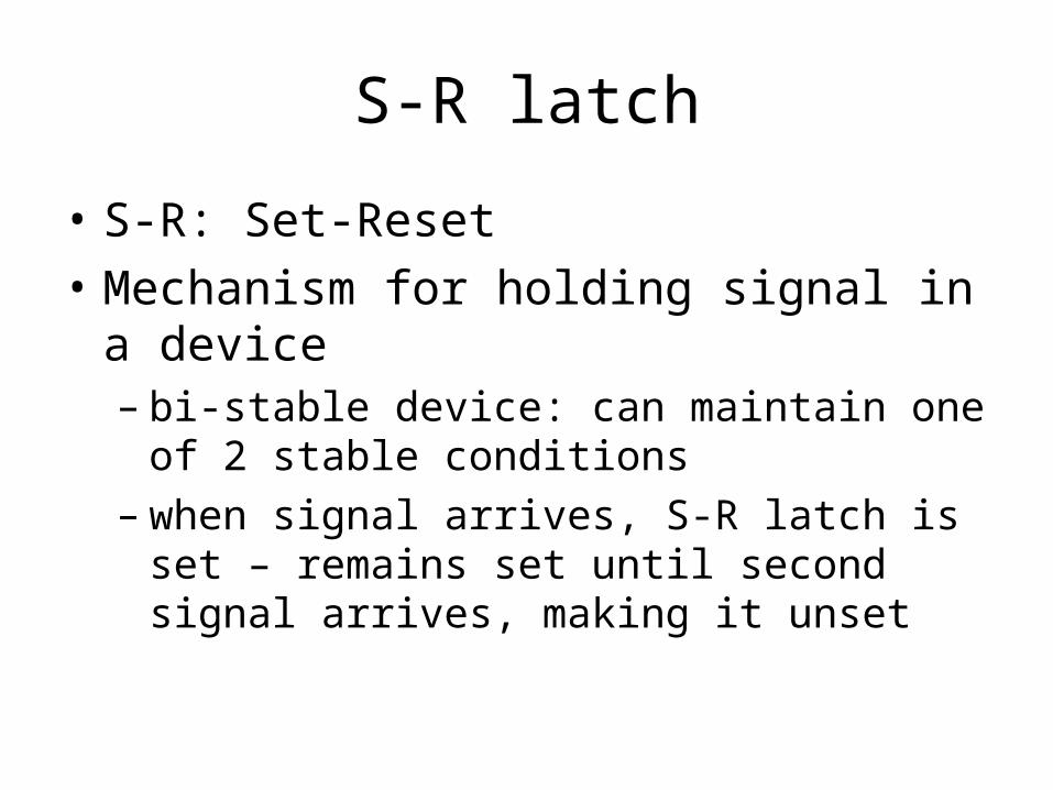
S-R latch
• S-R: Set-Reset• Mechanism for holding signal in a device
– bi-stable device: can maintain one of 2 stable conditions
– when signal arrives, S-R latch is set – remains set until second signal arrives, making it unset
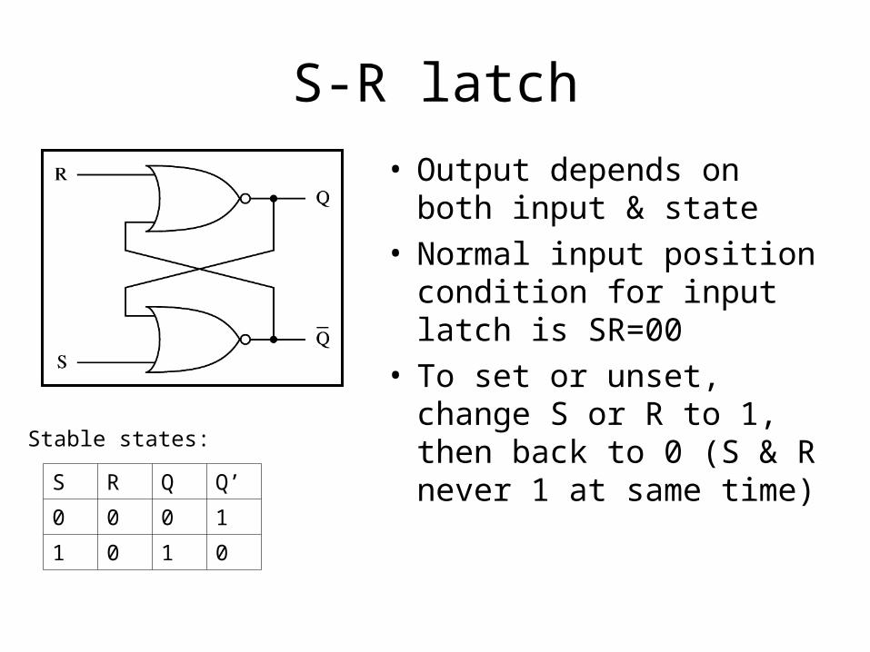
S-R latch• Output depends on both
input & state• Normal input position
condition for input latch is SR=00
• To set or unset, change S or R to 1, then back to 0 (S & R never 1 at same time)
Stable states:
S R Q Q’
0 0 0 1
1 0 1 0

Timing diagram for SR latch: 2 cycles
• Initial state: Q=0, Q’=1a) S gets 1; Q=1, Q’=0; when S goes back to 0, output doesn’t changeb) R gets 1; resets Q to 0, Q’ to 1 (initial state)c) S gets 1; sets Q to 1d) 1 to 0 transition in S; no changee) another reset; back to initial state

Clock pulses
• Signal sent at regular intervals• Time between pulses called period of clock• Shorter the period, faster the machine
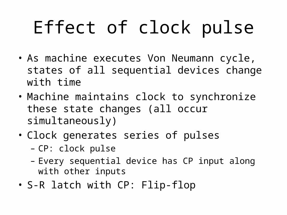
Effect of clock pulse
• As machine executes Von Neumann cycle, states of all sequential devices change with time
• Machine maintains clock to synchronize these state changes (all occur simultaneously)
• Clock generates series of pulses– CP: clock pulse– Every sequential device has CP input along with other
inputs
• S-R latch with CP: Flip-flop

Operation of sequential net
• t0: initial state
• t1: set (1) arrives @ S– passes through OR gate;
value true @ point a– signal negated; false @ b– since no signal has arrived
@ R, both R & b are false, so c is false
– At point 2, signal negated, so Q is true – this result is fed back to lower OR-gate
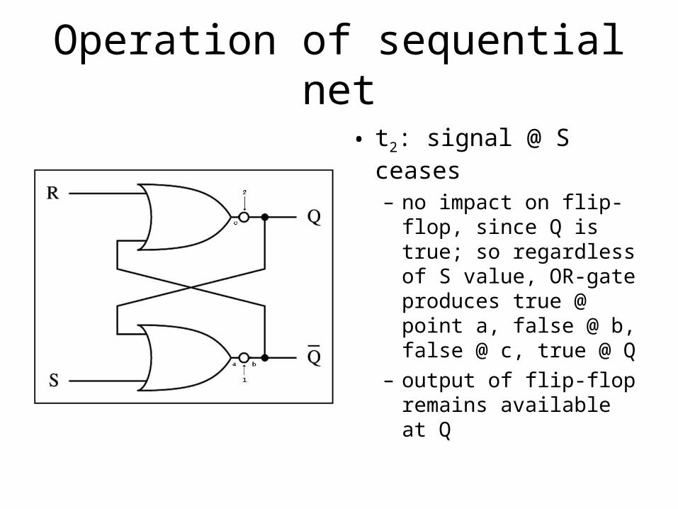
Operation of sequential net
• t2: signal @ S ceases– no impact on flip-flop,
since Q is true; so regardless of S value, OR-gate produces true @ point a, false @ b, false @ c, true @ Q
– output of flip-flop remains available at Q

Flip-flop symmetry
• Provides mechanism for terminating set state
• Reset mechanism– Signal @ R causes change at
point c, Q=false– This cuts off support to bottom
gate – signal now high @ Q’, low @ Q
– If a second signal arrived @ S before signal arrived @ R, no change to outputs
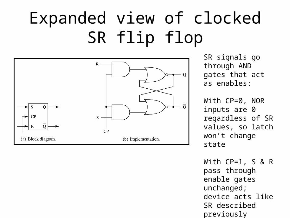
Expanded view of clocked SR flip flop
SR signals go through AND gates that act as enables:
With CP=0, NOR inputs are 0 regardless of SR values, so latch won’t change state
With CP=1, S & R pass through enable gates unchanged; device acts like SR described previously
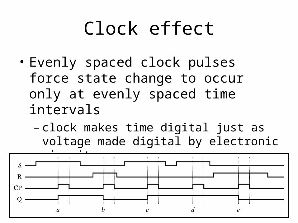
Clock effect
• Evenly spaced clock pulses force state change to occur only at evenly spaced time intervals– clock makes time digital just as voltage made
digital by electronic circuitry– state change can only occur at pulse, not between
them

Level-sensitive flip-flop
• Latch responds to CP only when CP high• Can cause problem when combined with
combinational devices in feedback loop: can lead to unstable state every few gate delays
• Need:– SR constrained by CP– immune to further changes through feedback
connection– sensitive to input for extremely short time period

Techniques for addressing level-sensitive flip flop problem
• Edge-triggered flip flop: sensitive to input only when clock is making transition from low to high
• Master-slave flip flop
Diagram at left: timing detail of single clock pulse
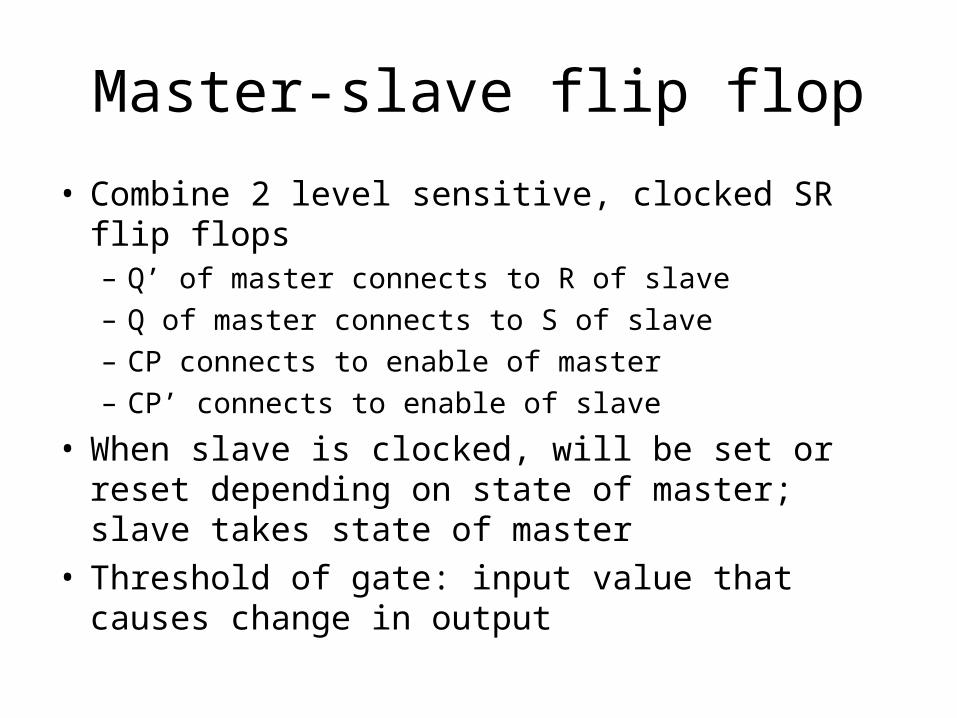
Master-slave flip flop
• Combine 2 level sensitive, clocked SR flip flops– Q’ of master connects to R of slave– Q of master connects to S of slave– CP connects to enable of master– CP’ connects to enable of slave
• When slave is clocked, will be set or reset depending on state of master; slave takes state of master
• Threshold of gate: input value that causes change in output

Timing detail of single clock pulse
• t1: isolate slave from master– signal reaches threshold of
master; inverter output goes 1 to 0
– slave now shielded from its own SR inputs
• t2: connect master to input– signal reaches threshold of
master enable gates– master now sensitive to SR
inputs, but change in master can’t affect slave

Timing detail of single clock pulse
• t3: isolate master from input– CP in high to low transition– master becomes insensitive
to input– slave still isolated
• t4: connect slave to master– CP now below inverter
threshold– output goes 0 to 1, slave now
connected to master– slave assumes state of master

Master-slave flip flop

Timing diagram of master-slave SR flip flop
• Clock transition not instantaneous; gradually increase from V1 to V2, decreases through V2, V1
• Change occurs in Q (state of slave latch) when slave is connected to master (at time t4 – during CP transition from hight to low

Representing flip flop states
• Flip flop is sequential, not combinatorial – can’t describe using truth table
• Alternatives:– Finite state machine– Characteristic table

Characteristic table
• Specifies state of device after one clock pulse for given input & initial state
• Similar to state transition table for FSM
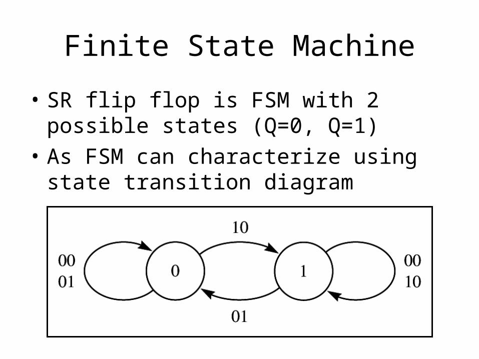
Finite State Machine
• SR flip flop is FSM with 2 possible states (Q=0, Q=1)
• As FSM can characterize using state transition diagram