Working With Flip-Flops
6
shown in Fig. 2 . That way high input sig- nals can reach the S-R Hip-Hop only w hen the cloclc ti signal is also high. There- fbrc. when C I I is low, hot11 inputs of the flin-tfop are held low, irrcspcctive o [he . states of the SET and li ts~r nputs. so the flip-flop functions as a 'permanent" nlemory. However, when -LX is high, the circuit functions as n standard S--R Hip- flop. Conseq~~ently, nformation is not au- tomaticailv latched into the H~D-HOD but Flip flops are the basis of all digital circuits. Learn must be "I-~ocl<eci" n; that's w'hy tie cir- about the different typas and practical applications for them. cuit is known as a clocked S -R Hip-flop. Figure 3-0 shows how to make the most RAY MARSTON table in c. I)IC;I.I.AL. IC S CAN HEC L.ASSIFIED INTOl WO basic types: gates and flip-flops. The latter are ;~lso nown as bistable latches and Inenlory elements. Many devices are based o n Hip-flops, including counters, dividers, shift registers, data latches, etc ., as well as presettable upidown counters and dividers, and other devices. In this article we will explain how sever- al types of Hip-flops work. Then we'll go on to ciiscuss several versatile CM OS flio- simple memory element that "reinem- bers" which of the two inputs last went high. Note, however, that the output state cannot be predicted if both inputs go high sin1ultaneously, so that ril~ist not be al- lowed to occur. Fig. l-b shows the symbol of the S-R tlip-flop, aiid Fig. I- , shows its truth table. The versatility of the basic c irc~iit an be enhanced greatly by wiring an AND gate in series with each input terminal as flops. Last, we'll show many practical circuits that use flip-flops. Basic principles The simplest type of CMOS flip-flop is the cross-coupled bistable latch shown in Fig. -(I. The circuit is built from two NOR gatcs; it has two inputs (usually tied low via pull-down resistors), and a pair of o~lt- from two AND gates, in addition to the S-R flip- of-ohase outnuts. The circuit works like flop. irnp<qrtant o f a11 flip-flops, the clocked master-slave flip-flop. It's built from two clocked S-R flip-flops that are cascaded and clocked out of phase via an inverter in thc clock line. It works a s t0llows. When the (,[.ti input is low, t he inputs to the m aster flip.-l lop are enabled via the inverter, so the SL:.I,-RESET data is accepted. However, the inputs to the slave fl ip-flop are disabled, s o the data is not passed to the output terminals. Then, when the CI.K input goes high, the inputs to the ~n as ter ip-tlop are disabled. so the input data is latched in the outputs; simultaneously, the input to the slave Hip- flop is enabled, and the latched data is passed to the c)tltput terminals. The sym- bol of the clocked master-slave Hip-Hop is shown in Fig. 3-h. The clocked master-slave flip-Hop can be made to toggle (or divide by two) by cross-coupling the input and output termi- nals as shown in Fig. 4-(1. By doing so. SE.~ nd (and KESE.~ ncl Q are always at opposite logic levels. So when CLK goes FIG. 4- THE TOGGLE ORT YPE -T FLIP-FLOP a) s built fr om a clocked master-slave flip-flop. Its symbol is shown in b this: If the sr:-r terminal is brieHy taken high, the outpl~t mmediately goes high, and the outp~lt goes low. The cross- coupling between the two gates causes the o~~tputs o latch in that state. even when both inpu ts are pulled low again. The only way the output states can be changed is by applying a high to the RESET terminal, in which case the Q output immediately goes low, and the utput goes high. Again, cross-coupling causes the outp~lts o latch into the new state even when both inputs ale pulled low. Because of the latching action, the basic Set-Reset (S-R) Hip- flop acts as a NOR gate A B Output 0 0 1 1 0 0 0 1 0 1 1 0
-
Upload
john-apostle -
Category
Documents
-
view
215 -
download
0
Transcript of Working With Flip-Flops
8/19/2019 Working With Flip-Flops
http://slidepdf.com/reader/full/working-with-flip-flops 1/6
shown in Fig. 2. That way high input sig-
nals can reach the S-R Hip-Hop only w hen
the cloclc ti signal is also high. Th ere-
fbrc. when CI I is low, hot11 inputs o f the
flin-tfop are held low, irrcspcctive o [he
.
states of the SET and l i t s ~ rnputs. so the
f l ip-f lop funct ions as a 'permanent"
nlemory. However, when
- L X
is high, the
circuit functions as
n
standard S--R Hip-
flop. Conseq~~ently,nformation is not au-
tomaticailv latched into the H~D-HOD but
Flip flops are the basis of all digital circuits. Learn
must be "I-~ocl<eci" n; that's w'hy t i e cir-
about the different typas and practical applications for them .
cuit is known as a clocked S -R Hip-flop.
Figure
3-0
show s how to make the most
RAY MARSTON
table in c.
I)IC;I.I.AL. IC S C A N HEC L.ASSIFIED
INTOl WO
basic types: gates and flip-flops. The latter
are ;~ ls o nown as bistable latches and
Inenlory elements. Many devices are
based o n Hip-flops, including counters,
dividers , shift registers, data latches, etc .,
as well as presettable upidown counters
and dividers, and other devices.
In this article we will explain ho w sever-
al types of Hip-flops work . Then we'll g o
on to ciiscuss several versatile CM OS flio-
simple memory element that "reinem-
bers" which of the two inputs last went
high. Note, however, that the output state
cannot be predicted if both inputs go high
sin1ultaneously, so that ril~istnot be al-
lowed to occur. Fig. l-b shows the sym bol
of the S-R tlip-flop, aiid Fig. I - , shows its
truth table.
The versatility of the basic c irc ~ii t an
be enhanced greatly by wiring an
A N D
gate in series with each input terminal as
flops. Last , we'll show many practical
circuits that use flip-flops.
Basic principles
The simplest type of CMO S flip-flop is
the cross-coupled bistable latch shown in
Fig. -(I. The circuit is built from two N O R
gatcs; it has two inputs (usually tied low
via pull-down resistors), and a pair
of
o ~ l t -
from two AND gates, in addition to the S-R flip-
of-ohase outnuts. The circuit works like
flop.
irnp<qrtant
of
a11 flip-flops, the clocked
master-slave flip-flop. It's built from two
clocked S-R flip-flops that are cascaded
and clocked out of phase via an inverter in
thc clock line.
It works as t0llows. When the (,[. ti input
is low, the inputs to the m aster flip.-llop are
enabled via the inverter, so the SL:.I,-RESET
data is accepted. However, the inputs to
the slave flip-flop are disab led, s o the data
is not passed to the output terminals.
Then, when the CI.K input goes high, the
inputs to the ~n as te r ip-tlop are disabled.
so the input data is latched in the outpu ts;
simultan eously, the input to the slave Hip-
flop is enabled, and the latched data is
passed to the c)tltput terminals. The sym-
bol of the clocked master-slave Hip-Hop is
shown in Fig.
3-h.
The clocked master-slave flip-Hop can
be made to toggle (or divide by two) by
cross-coupling the input and output termi-
nals as shown in Fig. 4-(1. By doing so.
S E . ~ nd (and
K E S E . ~
ncl Q are always at
opposite logic levels. So when
CLK
goes
FIG. 4-THE TOGGLE ORT YPE -T FLIP-FLOP a)
s
built from a clocked master-slave flip-flop. Its
symbol is shown in b
this: If the sr:-r terminal is brieHy taken
high, the ou tpl~ tmmediately goes high,
and the ou tp~ ltgoes low. The cross-
coup ling between the two gates causes the
o ~ ~ t p u t so latch in that state. even when
both inpu ts are pulled low again. The only
way the output states can be chan ged is by
applying a high to the RESET terminal, in
which cas e the Q output immediately goes
low, and the utput goes hig h. Again ,
cross-coupling causes the outp ~ltso latch
into the new state even when both inputs
ale
pulled low.
Because of the latching action, the
basic S et-Reset (S -R ) Hip-flop acts as a
NOR gate
A B Output
0 0 1
1 0 0
0 1 0
1 1 0
8/19/2019 Working With Flip-Flops
http://slidepdf.com/reader/full/working-with-flip-flops 2/6
LK
goes high, the slave flip-flop
state. Note that the output states
ge on the arrival of the leading edge
It takes two clock pulses to change the
one state to another and back
known as a Toggle (o r type-T) flip-
D
flip-flop
The type-T flip-flop is a special device
tions only as a counteridivider. A
5- 1. In that circuit, an
s and
of phase, and the input
5-0
and
5-c show the sy ~n bo l nd the truth
of the type-D flip-flop, respectively.
type- D flip-flop can be used as a data
latch by connecting it as shown in Fig.
6- 1,
or as a binary cou nterid ivide r by con-
necting it as shown in Fig. 6-b.
The
JK
flip-flop
Figure 7-ti shows the basic circui t of
an
even more versat i le c locked f l ip- f lop ,
which is universally known as the
JK-
type. It can function eit her as a data latch,
a counteridivider, or as a do -nothing ele-
ment by suitably connec ting the J and K
terminals. The symbol of the
J K
flip-flop
is shown in Fig. 7-0, and its truth table is
shown in Fig. 7-c.
In essence , the JK flip-flop firnctions as
a T-type when inputs are both high , and as
a D-type when they're different. When
they're both low, the outputs remain un-
changed when a pulse arrives.
Real-world devices
The two best-known clocked CMOS
flip-flops are the 4013 D-type and the
4027 JK-type. Each 1C contains two inde-
pendent flip-flops that share power and
ground connections. Figure 8-0 shows the
THE DATA OR TYPE -D FLIP-FLOP a is built from a clocke d master-slave flip-flop. Its symbol
is
b, and its truth table in c.
a)or as a divide-by-two counter
c)
functional diagram of the 4013; the truth
table of its clocked inp uts is shown in Fig.
8- h . and that of its direct inputs is shown
in Fig. 8-c . Corresponding diagrams for
the 4027 are shown in Fig. 9-ti , Fig. 9 4 ,
and Fig.
9 c.
Note that both the 4013 and the 4027
have SET and RESET inputs in addition to
the normal clocked inputs. For both IC's
K FLIP-FLOP S CIRCUIT is shown in
a,
along with its symbol b)and action table
c.)
those terminals are direct inputs that en-
able the clocked action of the flip-flop to
be overridden, in which case the device
functions as a simple unclocked S-R flip-
flop. For normal clocked operation, the
direct inputs must be grounded.
The 4013 and 4027 are fast-actin g, so it
is important that their clock signals be
absolutely noise-free and bounce less, and
that they have risetimes and
falltimes of
less than five ps. Both IC's clock on the
positive transition of the clock signal.
Ripple counters
The most popular application of the
clocked flip-flop is as a binary counter.
Fig.
10-0
shows how to connect the 4013
as a divide-by-two counter; Fig. 10-h
shows the corresponding connections for
the 4027. When clocked by a fixed-fre-
quency waveform, both circuits give a
symmetrical square-wave output at half
the clock frequency.
As shown in Fig. 11, you can cascade
several ripple counters ( so called because
of the way that cl&k pulses appear to
ripple from stage to stage) to provide divi -
sion by successive powers of two. Figure
11-0 shows how to cascade two D-type
flip-flops, and Fig. 11-h shows how to
cascade two JK-type flip-flops to provide a
division ratio of 4 (2 x 2 or 2'). In a lik e
manner, Fig. 12-a and Fig. 12-0 show how
three stages can be cascaded to give a
division ratio of eight (23). In fact, an
arbitrary number of stages can be cas-
caded, as shown in Fig. 13, to provide a
division ratio of 211, where
z
is the num ber
of stages.
The circuits shown in Fig. 11-Fig. 13
are known as ripple counters, because
each stage is clocked by the ou tput of the
preceding stage, rather than by a master
clock signal. The effect, therefore, is that
the c lock s igna l s eems to r ipp le
through the counter chain . The problem is
that the propagation delays of all the di-
viders add together and provide a delay
that prevents the counter s tages from
clocking synchronously. Counters of that
sort are in fact called asy nchronous cou n-
ters. If the outputs of the stages are de-
coded via gate networks, output glitches
and inaccurate decoding can result.
Long ripple counters
Although 4013 and 4027 counters can
be cascaded to give any desired nu mb er of
stages, when more than four stages are
needed, it's usually economical to use a
special-purpose MSI r ipple-carry b~nary
counteridivider IC. Our next few figures
show several examples.
The 402 4, shown in Fig. 14, is a seven-
stage ripple counter; all seven outputs are r
externally accessible. The IC provides a
maximum division ratio of 128 (27). The
8/19/2019 Working With Flip-Flops
http://slidepdf.com/reader/full/working-with-flip-flops 3/6
FIG. 11-TO DIVIDE FREQUENCY BY FOUR you
can use a pair of D a) r JK b) lip-flops.
shown in b and c respectively.
FIG. 12-TO DIVIDE FREQUENCY BY EIGHT yoti
can use three D a) r JK b) lip-flops.
trary factor 2 , use n stages.
.
i n b and c respectively.
a 14-stage counter; all outputs except 2
and 3 are externally accessible. The 40 20
provides a maximum division ratio of
16,3 84 (214).
Figure 17-0 shows details of the 4060.
It is another 14 -stage device, but ou tputs
1, 2, 3, and I1 are not accessible. A spe-
cial feature of the
IC
is that it incorporates
a built-in oscillator circuit. As shown in
Fig. 17-6 and Fig. 17-c he device can use
can use a D
a)
or a JK b) lip-flop.
you
either a crystal or an RC network to set the
frequency of oscillation.
404 0, shown in Fig. 15, is a 12-stage de- The 402 0, 402 4, 4040, and 4060 IC s
vice, of which all outp uts are accessible. all have Schmitt-trigger inputs that trigger
It provides a maximum division ratio of
on the negative transition of each input
40 96 (21 ). The 40 20 , show n in Fig. 16, is
pulse. All of those counters can be set to
zero by applyin g a high level to the
RESET
line.
Glitches
A two-s ta ge d iv ide -by- four r ipp le
counter, like that shown in Fig. 18-a, can
have four possible output states, as shown
in Fig. 18-b. Both ou tputs can be high,
both can be low, one can be high and the
other low, or the former low an d the latter
high. Before any clock pulses have been
received, the Q and
QI
outputs are low.
When the first pulse arriv es, QIgoes high.
When the second pulse arrives,
2
goes
high and QI goes low. On the third pulse,
Q? and QIboth go high. L ast, on the fourth
pulse,
~ 7
nd
QI
both go low again.
8/19/2019 Working With Flip-Flops
http://slidepdf.com/reader/full/working-with-flip-flops 4/6
state, as shown in Fig. 18-c. Because the
Up and down counters.
ripple counter is an asynchronous dev ice,
A
stan dard ripp le co un ter co un ts u p
however, the propagation delay between
the decoded outpu ts increase in value with
the two flip-flops may cause glitches to
each succeeding clock pulse. It is possi-
14--PINOUT OF
THE
4024 seven-stage rip-
15-PINOUT OF THE 4040 12-stage ripple
(120~tputs espond to (he input signal as shown in bywhen they re combined as shown in c a glitch
may be generated, as shown in
d
G. IGPI NO UT OF
TH
4020 14-stage ripple
Each of the four possible states can be
provide four unique ou tputs by
he outputs that are unique to each
appear in the decoded o utputs, as shown
in Fig. 18-d. f course, those types of
glitches are possib le with any m ulti-stage
ripple counter, and the greater the numbe r
of stages, the gr eater the total propagation
delay b ecomes, and the greater the prob-
lem with glitches. The solution to the
glitch problem is to use a clocked-logic
device, which we ll discu ss momentarily.
ble, however, to build a counter that works
in the opposite direction. That type of
counter is called a down (or a subtract)
counter. The circuit is shown in Fig. 19-a;
its truth table is shown in Fig. 19-b.
Walking-ring Johnson) counters
Ripple counters are useful where un-
decoded binary division is needed, but
8/19/2019 Working With Flip-Flops
http://slidepdf.com/reader/full/working-with-flip-flops 5/6
FIG. 19--A DOWN-COUNTING RIPPLE COUNTER is shown in a; the truth-table is shown inb.
1
SET
2 OW
1 CHANGESTAT
SET
2
HIGH
1
1 CHANGESTAT
-
-
SET 2 OW 1 SET Q l OW
.
.
-
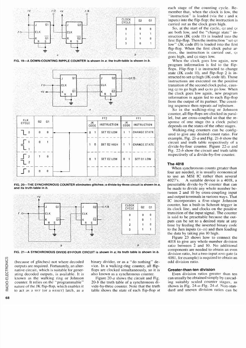
FIG. 20--THE SYNCHRONOUS COUNTER eliminates glitches; a divide-by-three circuit is shown in a
and its truth-table in b.
FIG. 21-A SYNCHRONOUS DIVIDE-BY-FOUR CIRCUIT is shown
in
a; its truth table is shown
n b.
(because of glitches) not where decoded
outp uts are requ ired. Fortunately, an alter-
native circuit, which is suitable for gener-
ating decoded outputs, is available. It is
known as the walking ring or Johnson
counter. It relies on the pro gra n~ ma ble
nature of the JK flip-flop. which ena bles it
to act as a SET (or a RESET latch, as a
binary divider, or as a do nothing de-
vice. In a walking-ring counter, all flip-
flops are clocked simultaneously, so it is
also known as a synchronous counter.
Figure 20-0 shows the circuit and Fig.
20-b the truth table of a synchronous di-
vide-by-three counter. Note that the truth
table shows the state of each flip-flop at
each stage of the counting cycle. Re-
member that, when the clock is low, the
instruction is loaded (via the I and K
inputs ) into the flip-flop; the instruction is
carried out as the clock goes high.
So, at the start of the cycle,
~z
and QI
are both low, and the chang e state in-
struction (JK code 11) is loaded into the
first flip-flop. Then the ins truc tion set 0 2
low (JK cod e 01) is loaded into the first
flip-flop. When the first clock pulse ar-
rives. the instruction is carried out, QI
goes high, and ~ 2 stays low.
When the clock goes low again, new
program information is fed to the flip-
flops. Flip-flop is instructed to chang e
state (JK code ll), and flip-flop 2 is in-
structed to set 4 2 high (JK co de 10). Tho se
instructions are executed on the positive
transition of the second clock p ulse, caus-
ing ~ 2 to go high and QI to go low. When
the clock goes low again, new program
information is again fed to each flip-flop
from the output of its partner. The count-
ing sequence then repeats a d
injniturn
So i n t he wa l k i ng- r i ng or Johnson
counter, all flip-flops are clocke d in p aral-
lel, but are cross-coupled so that the re-
sponse of one stage (to a clock pulse)
depends o n the states of the other stages.
Walking-ring counters can be config-
ured to give any desired count ratio. For
exam ple, Fig. 21-a and Fig. 21-b show the
circuit and truth table respectively of a
divide-by-four counter. Figure 22-n and
Fig. 22-h show the circuit and truth table
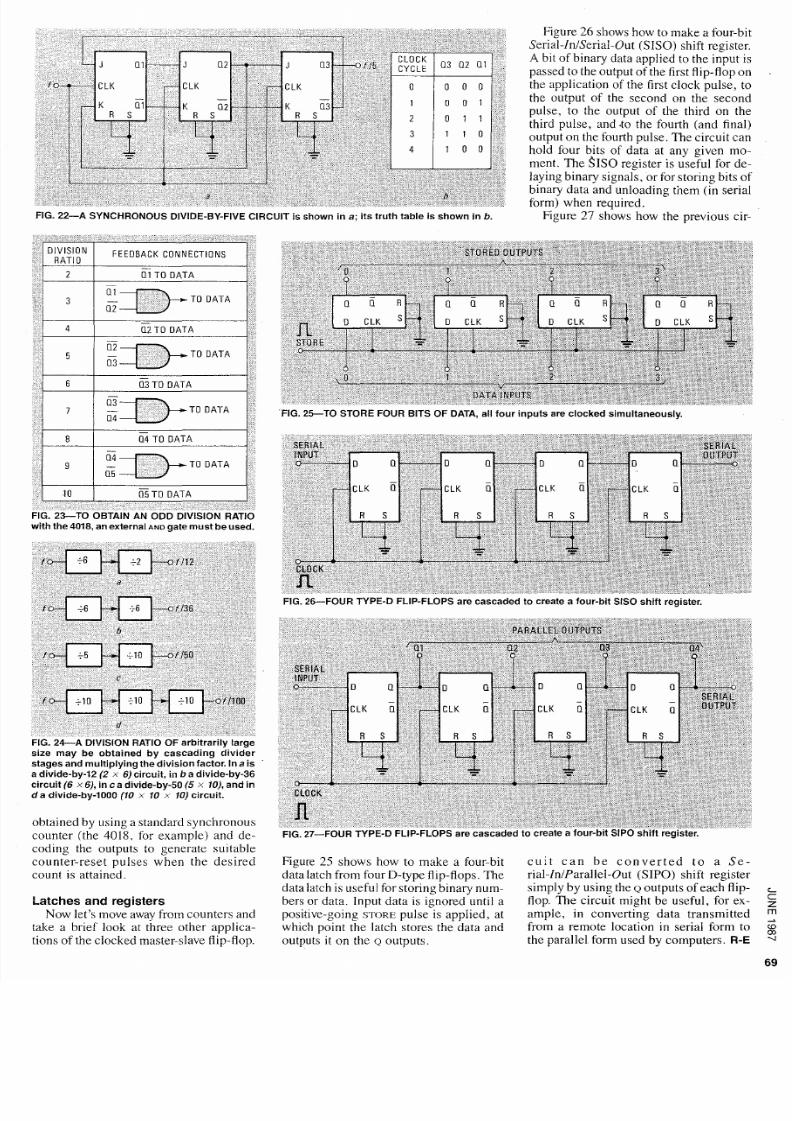
respectively of a divide-by-five counter.
The 4018
When synchro nous counts greater than
four are needed, it is usually economical
to use an MSI
IC
rather then several
4027's. A suitable device is a 4018, a
presettable divide-by-N counter that can
be made to divide any whole num ber be-
tween 2 and 10 by cross-coupling input
and outp ut terminals in various ways. Th at
IC incorpora tes a f ive-s tage Johnson
counter, has a built-in Schmitt trigger in
its clock line, and clocks on the positive
transition of the input signal. The counter
is said to be presettable because the out-
puts can be set to a desired state at any
time by feeding the inverted binary code
to the Jam inputs 11-~5) and then loading
the data by taking pin 10 high.
Figure 23 shows how to connect the
4018 to give any whole-number division
ratio between 2 and 10. No additional
compon ents are needed to obtain an even
division ratio, but a two-input A N D gate (a
4081, for examp le) is required to obtain an
odd division ratio.
Greater than ten division
Even division ratios greater than ten
can ~ ~ s u a l l ye obtained simply by cascad -
ing suitably scaled counter stages, as
shown in Fig. 24-a-Fig.
24-d. Non-stan-
dard and uneven division ratios can be
8/19/2019 Working With Flip-Flops
http://slidepdf.com/reader/full/working-with-flip-flops 6/6
Figure 26 shows how to make a four-bit
Serial-InISerial-Out (SIS O) shift register.
A
bit of binary data applied to the input is
passed to the output of the first flip-flop on
the application of the first clock pulse, to
the output of the second on the second
pulse. to the output of the third on the
third pulse, and
.to the fourth (and final)
output on the fourth pulse. The circuit can
hold four bits of data at any given mo-
ment. The
1~0
egister is useful for de-
laying binary signals. or for storing bits of
binary data and unloading them (in serial
form) when reauired.
IG. 22-A SYNCHRONOUS DIVIDE-BY-FIVE CIRCUIT is shown in a; i ts truth table is shown in b.
Figure
27
shbws how the previous cir-
FIG. 2 G T O STORE FOUR BITS OF DATA, a ll four inputs are clocked simultaneously.
3--TO OBTAIN AN ODD DIVISION RATIO
the 4018, an externalAND gate must be used.
FIG. 26 FOUR TYPE-D FLIP-FLOPS are cascaded to create a four-bit SISO shif t register.
d multiply ing the division factor. Ina is
2
x
6) circuit, in
b
a divide-by-36
x E , in c a divide-by-50
5
x lo),and in
a divide-by-1000
10x 10 x 10)
circuit.
4018. for ex am ~ le ) nd de-
g the outp uts to geneiat; suitab le
pulses when the desired Figure 25 s ho w s h ow t o m ak e a fou r-b it c u i t c a n b e c o n v e r t e d t o a S e -
data latch from four D-type flip-flo ps. The rial-lnIParalle1-Out (SIPO ) shift registe r
data latch is useful for storin g binary num - simply by using the Q outp uts of each flip-
nd
registers
bers or data. Input data is ignored until a flop. The circuit might be useful, for ex-
Now let s move away from coun ters and positive-going STOR pulse is applied. at
ample, in converting data transmitted
brief look at three other applica- which point the latch stores the data and
from a remote location in serial form to
outputs it on the Q outputs.
the parallel form used
by
computers. R E