Basic Flip Flops
9
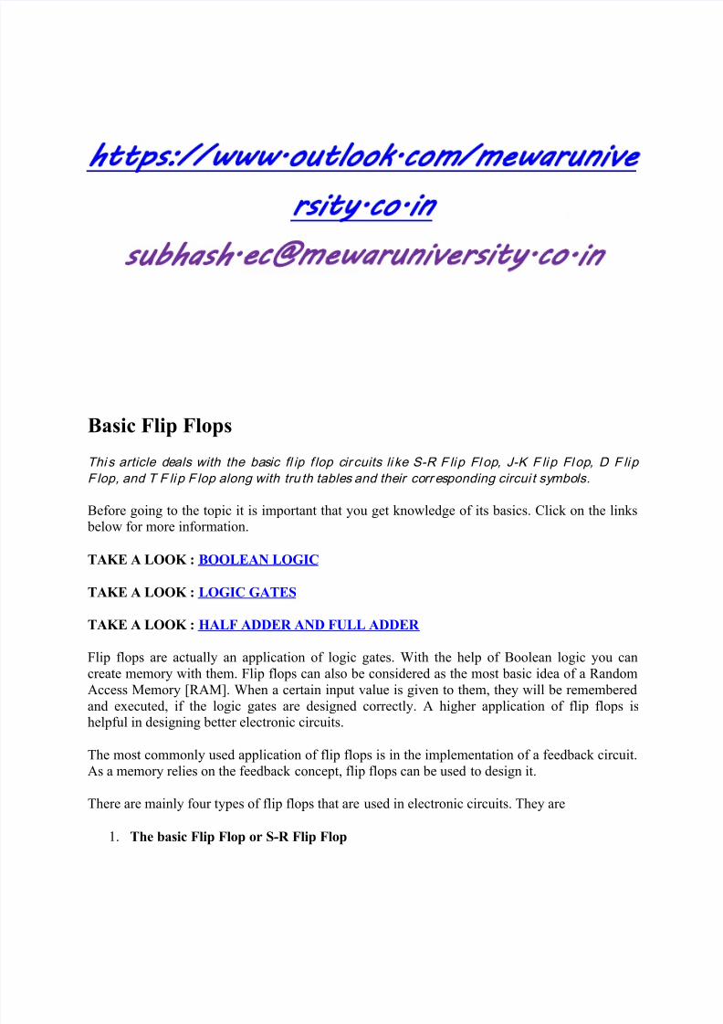
https://www.outlook.com/mewarunive rsity.co.in [email protected] Basic Flip Flops This article deals with the ba s ic fl ip f lop cir cuits like S-R F li p Fl op, J-K F li p Fl op, D F li p F lop, and T F li p F lop along with tru th tables and their corr e s ponding circui t sy mbols. Before going to the topic it is important that you get knowledge of its basics. Click on the links below for more information. TAKE A LOOK : BOOLEAN LOGIC TAKE A LOOK : LOGIC GATES TAKE A LOOK : HALF ADDER AND FULL ADDER Flip flops are actually an application of logic gates. With the help of Boolean logic you can create memory with them. Flip flops can also be considered as the most basic idea of a Random Access Memory [RAM]. When a certain input value is given to them, they will be remembered and executed, if the logic gates are designed correctly. A higher application of flip flops is helpful in designing better electronic circuits. The most commonly used application of flip flops is in the implementation of a feedback circuit. As a memory relies on the feedback concept, flip flops can be used to design it. There are mainly four types of flip flops that are used in electronic circuits. They are 1. The basic Flip Flop or S-R Flip Flop
-
Upload
subhash-kumar -
Category
Documents
-
view
230 -
download
0
Transcript of Basic Flip Flops
7/28/2019 Basic Flip Flops
http://slidepdf.com/reader/full/basic-flip-flops 1/9
https://www.outlook.com/mewarunive
rsity.co.in
Basic Flip Flops
Thi s article deals with the basic fl ip f lop cir cuits li ke S-R F lip Flop, J-K F lip Flop, D F lip
F lop, and T F lip F lop along with tru th tables and their corr esponding circui t symbols.
Before going to the topic it is important that you get knowledge of its basics. Click on the links below for more information.
TAKE A LOOK : BOOLEAN LOGIC
TAKE A LOOK : LOGIC GATES
TAKE A LOOK : HALF ADDER AND FULL ADDER
Flip flops are actually an application of logic gates. With the help of Boolean logic you can
create memory with them. Flip flops can also be considered as the most basic idea of a Random
Access Memory [RAM]. When a certain input value is given to them, they will be remembered
and executed, if the logic gates are designed correctly. A higher application of flip flops is
helpful in designing better electronic circuits.
The most commonly used application of flip flops is in the implementation of a feedback circuit.
As a memory relies on the feedback concept, flip flops can be used to design it.
There are mainly four types of flip flops that are used in electronic circuits. They are
1. The basic Flip Flop or S-R Flip Flop
7/28/2019 Basic Flip Flops
http://slidepdf.com/reader/full/basic-flip-flops 2/9
2. Delay Flip Flop [D Flip Flop]
3. J-K Flip Flop
4. T Flip Flop
1. S-R Flip Flop
The SET-RESET flip flop is designed with the help of two NOR gates and also two NAND
gates. These flip flops are also called S-R Latch.
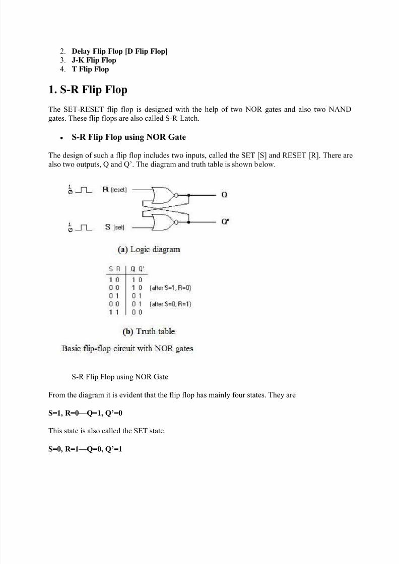
S-R Flip Flop using NOR Gate
The design of such a flip flop includes two inputs, called the SET [S] and RESET [R]. There are
also two outputs, Q and Q’. The diagram and truth table is shown below.
S-R Flip Flop using NOR Gate
From the diagram it is evident that the flip flop has mainly four states. They are
S=1, R=0 —Q=1, Q’=0
This state is also called the SET state.
S=0, R=1 —Q=0, Q’=1
7/28/2019 Basic Flip Flops
http://slidepdf.com/reader/full/basic-flip-flops 3/9
This state is known as the RESET state.
In both the states you can see that the outputs are just compliments of each other and that thevalue of Q follows the value of S.
S=0, R=0 —Q & Q’ = Remember
If both the values of S and R are switched to 0, then the circuit remembers the value of S and R in their previous state.
S=1, R=1 —Q=0, Q’=0 [Invalid]
This is an invalid state because the values of both Q and Q’ are 0. They are supposed to be
compliments of each other. Normally, this state must be avoided.
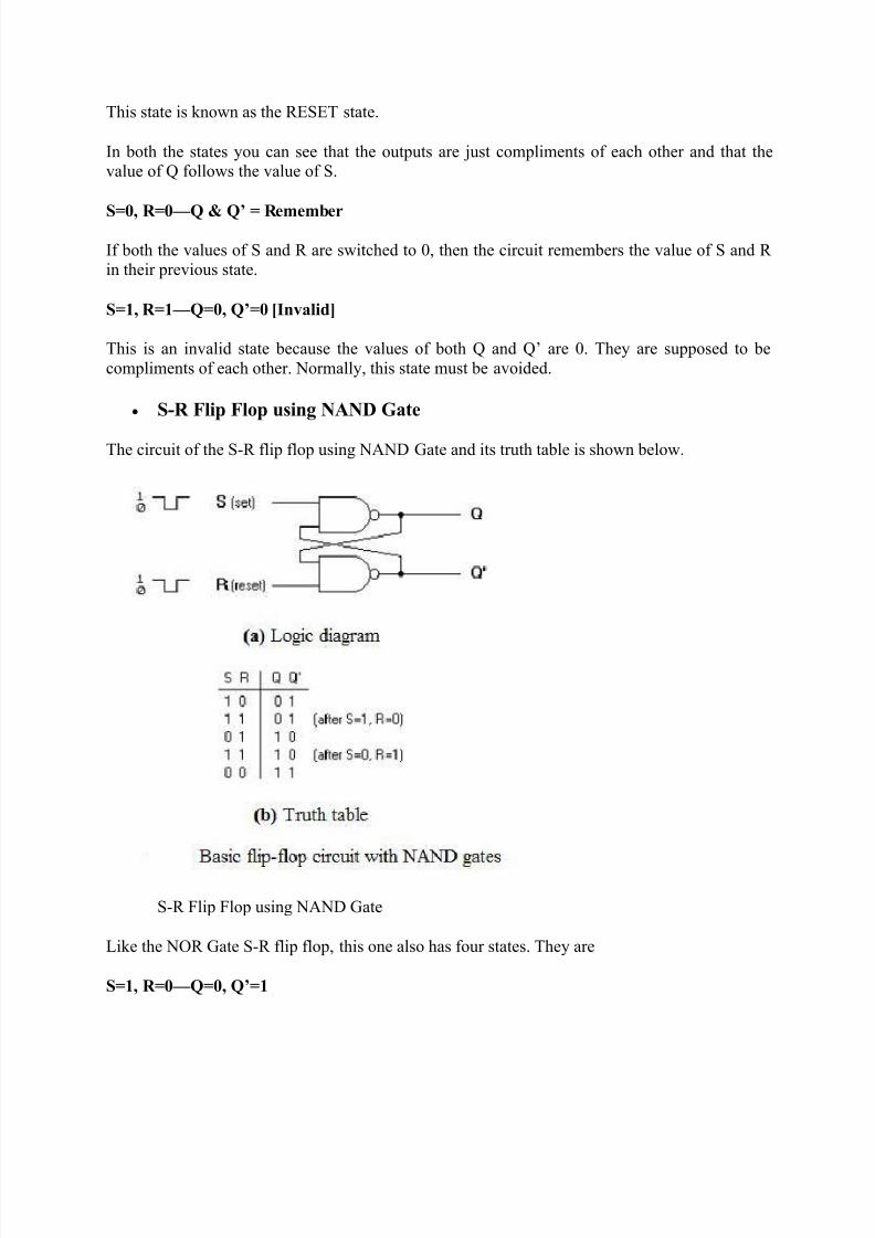
S-R Flip Flop using NAND Gate
The circuit of the S-R flip flop using NAND Gate and its truth table is shown below.
S-R Flip Flop using NAND Gate
Like the NOR Gate S-R flip flop, this one also has four states. They are
S=1, R=0 —Q=0, Q’=1
7/28/2019 Basic Flip Flops
http://slidepdf.com/reader/full/basic-flip-flops 4/9
This state is also called the SET state.
S=0, R=1 —Q=1, Q’=0
This state is known as the RESET state.
In both the states you can see that the outputs are just compliments of each other and that the
value of Q follows the compliment value of S.
S=0, R=0 —Q=1, & Q’ =1 [Invalid]
If both the values of S and R are switched to 0 it is an invalid state because the values of both Q
and Q’ are 1. They are supposed to be compliments of each other. Normally, this state must be
avoided.
S=1, R=1 —Q & Q’= Remember
If both the values of S and R are switched to 1, then the circuit remembers the value of S and R
in their previous state.
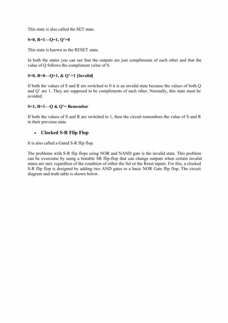
Clocked S-R Flip Flop
It is also called a Gated S-R flip flop.
The problems with S-R flip flops using NOR and NAND gate is the invalid state. This problem
can be overcome by using a bistable SR flip-flop that can change outputs when certain invalidstates are met, regardless of the condition of either the Set or the Reset inputs. For this, a clocked
S-R flip flop is designed by adding two AND gates to a basic NOR Gate flip flop. The circuitdiagram and truth table is shown below.
7/28/2019 Basic Flip Flops
http://slidepdf.com/reader/full/basic-flip-flops 5/9
Clocked S-R Flip Flop
A clock pulse [CP] is given to the inputs of the AND Gate. When the value of the clock pulse is’0′, the outputs of both the AND Gates remain ’0′. As soon as a pulse is given the value of CPturns ’1′. This makes the values at S and R to pass through the NOR Gate flip flop. But when the
values of both S and R values turn ’1′, the HIGH value of CP causes both of them to turn to ’0′
for a short moment. As soon as the pulse is removed, the flip flop state becomes intermediate.Thus either of the two states may be caused, and it depends on whether the set or reset input of
the flip-flop remains a ’1′ longer than the transition to ’0′ at the end of the pulse. Thus the invalid
states can be eliminated.
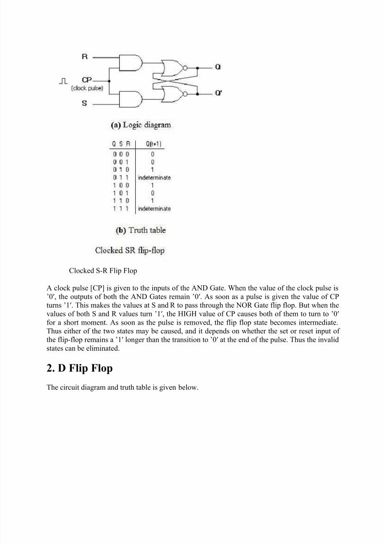
2. D Flip Flop
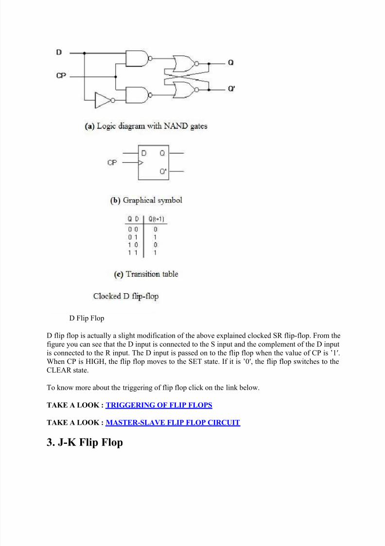
The circuit diagram and truth table is given below.
7/28/2019 Basic Flip Flops
http://slidepdf.com/reader/full/basic-flip-flops 6/9
D Flip Flop
D flip flop is actually a slight modification of the above explained clocked SR flip-flop. From the
figure you can see that the D input is connected to the S input and the complement of the D input
is connected to the R input. The D input is passed on to the flip flop when the value of CP is ’1′.When CP is HIGH, the flip flop moves to the SET state. If it is ’0′, the flip flop switches to the
CLEAR state.
To know more about the triggering of flip flop click on the link below.
TAKE A LOOK : TRIGGERING OF FLIP FLOPS
TAKE A LOOK : MASTER-SLAVE FLIP FLOP CIRCUIT
3. J-K Flip Flop
7/28/2019 Basic Flip Flops
http://slidepdf.com/reader/full/basic-flip-flops 7/9
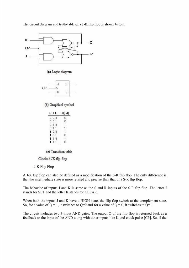
The circuit diagram and truth-table of a J-K flip flop is shown below.
J-K Flip Flop
A J-K flip flop can also be defined as a modification of the S-R flip flop. The only difference isthat the intermediate state is more refined and precise than that of a S-R flip flop.
The behavior of inputs J and K is same as the S and R inputs of the S-R flip flop. The letter Jstands for SET and the letter K stands for CLEAR.
When both the inputs J and K have a HIGH state, the flip-flop switch to the complement state.So, for a value of Q = 1, it switches to Q=0 and for a value of Q = 0, it switches to Q=1.
The circuit includes two 3-input AND gates. The output Q of the flip flop is returned back as afeedback to the input of the AND along with other inputs like K and clock pulse [CP]. So, if the
7/28/2019 Basic Flip Flops
http://slidepdf.com/reader/full/basic-flip-flops 8/9
value of CP is ’1′, the flip flop gets a CLEAR signal and with the condition that the value of Q
was earlier 1. Similarly output Q’ of the flip flop is given as a feedback to the input of the AND
along with other inputs like J and clock pulse [CP]. So the output becomes SET when the valueof CP is 1 only if the value of Q’ was earlier 1.
The output may be repeated in transitions once they have been complimented for J=K=1 becauseof the feedback connection in the JK flip-flop. This can be avoided by setting a time duration
lesser than the propagation delay through the flip-flop. The restriction on the pulse width can be
eliminated with a master-slave or edge-triggered construction.
4. T Flip Flop
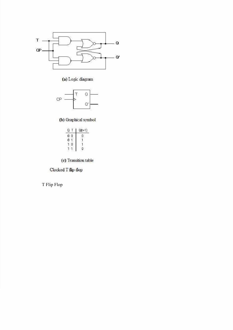
This is a much simpler version of the J-K flip flop. Both the J and K inputs are connectedtogether and thus are also called a single input J-K flip flop. When clock pulse is given to the flip
flop, the output begins to toggle. Here also the restriction on the pulse width can be eliminated
with a master-slave or edge-triggered construction. Take a look at the circuit and truth table
below.
7/28/2019 Basic Flip Flops
http://slidepdf.com/reader/full/basic-flip-flops 9/9
T Flip Flop