COMBINATIONAL CIRCUITS & FLIP FLOPS
25
COMBINATIONAL CIRCUITS & FLIP FLOPS
-
Upload
starlee-lathong -
Category
Documents
-
view
93 -
download
4
Transcript of COMBINATIONAL CIRCUITS & FLIP FLOPS

COMBINATIONAL CIRCUITS
&
FLIP FLOPS

Combinational Circuit A combinational circuit is a connected arrangement of
logic gates with a set of inputs and outputs. A block diagram of a combinational circuit is shown in
figure. The n binary input variables come from an external source, the m binary output variables go to an external destination and in between there is an interconnection of logic gates.

Designing a Circuit The problem is stated. The input and output variables are assigned letter
symbols. The truth table is derived. The simplified Boolean functions are obtained. The logic diagram is drawn.

Half Adder Addition of two binary digits. The input variables are called the augend and
addend bits. The output variables are sum and carry.

The C output is 0 unless both inputs are 1. The S output represents the least significant bit of the sum. The Boolean functions for the two outputs can be obtained directly from the truth table:
S = x'y + xy' = x ⊕ y
C = xy

Full Adder Arithmetic sum of three input bits. It consists of three inputs and two outputs. Two of the input variables, denoted by x and y,
represent the two significant bits to be added. The third input, z, represents the carry from the
previous lower significant position. The binary variable S gives the value of the least
significant bit of the sum. The binary variable C gives the output carry.

When all input bits are 0, the output is 0. The S output is equal to 1 when only one input is
equal to 1 or when all three inputs are equal to 1. The C output has a carry of 1 if two or three inputs
are equal to 1.

C= xy’z + x’yz + xy = z(xy’ + x’y) + xy = z(x ⊕ y) + xy S = xy’z’ + x’y’z + xyz + x’yz’ = z’(xy’ + x’y) + z(x’y’ + xy) = z’(x ⊕ y) + z(x ⊕ y)’ = a’b + ab’ (let a=z, b=x ⊕ y) = x ⊕ y ⊕ z

Boolean function: S=x ⊕ y ⊕ z C = xy + (x ⊕ y)z

Flip Flops A flip-flop is a binary cell capable of storing one
bit of information. It has two outputs, one for the normal value and
one for the complement value of the bit stored in it.
A flip-flop maintains a binary state until directed by a clock pulse to switch states.

SR Flip Flop Three inputs, labelled S (for set), R (for reset), and C (for
clock). It has an output Q and sometimes the flip-flop has a
complemented output, which is indicated with a small circle at the other output terminal.
The arrowhead-shaped symbol in front of the letter C to designate a dynamic input.
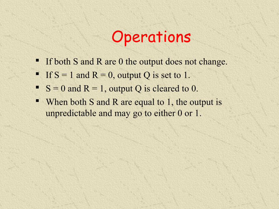
Operations If both S and R are 0 the output does not change. If S = 1 and R = 0, output Q is set to 1. S = 0 and R = 1, output Q is cleared to 0. When both S and R are equal to 1, the output is
unpredictable and may go to either 0 or 1.

D Flip Flop A slight modification of the SR flip-flop. An SR flip-flop is converted to a D flip-flop by inserting
an inverter between S and R and assigning the symbol D to the single input.

Operations If D = 1, the output of the flip-flop goes to the 1 state. D = 0, the output of the flip-flop goes to the 0 state. From the characteristic table we note that the next state
Q(t+1) is determined from the D input. The relationship can be expressed by a characteristic equation:
Q(t + 1) = D

JK Flip Flop A refinement of the SR flip-flop. Inputs J and K behave like inputs S and R
to set and clear the flip-flop, respectively.

Operations Same as an SR flip flop but when inputs J and K are both
equal to 1, a clock transition switches the outputs of the flip-flop to their complement state.
Q(t + 1) = Q'(t)

T Flip Flop Obtained from a JK type when inputs J and K are
connected to provide a single input designated by T.

Operations When T = 0 a clock transition does not change the state of the flip-flop. When T = l a clock transition complements
the state of the flip-flop. These conditions can be expressed by a characteristic equation:
Q(t + 1) = Q(t) ⊕ T

Edge-Triggered Flip-Flops Used to synchronize the state change during a
clock pulse transition. Some edge-triggered flip-flops cause transition on
the rising edge of the clock signal (positive-edge transition)
Others cause a transition on the falling edge (negative-edge transition).


The value in the D input is transferred to the Q output when the clock makes a positive transition. The output cannot change when the clock is in the 1 level, in the 0 level, or from the 1 to the 0 level.
In this case the flip-flop responds to a transition from the 1 level to the 0 level of the clock signal.

Another type of flip-flop used in some systems is the master-slave flip-flop. This type of circuit consists of two flip-flops.
The first is the master, which responds to the positive level of the clock,
The second is the slave, which responds to the negative level of the clock.
The result is that the output changes during the l-to-0 transition of the clock signal.

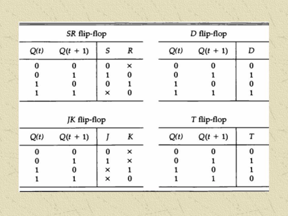
Excitation tables Movements of transitions to change states and to
find the flip-flop input conditions that will cause the required transition.

THANK YOU