Dual JK Flip-Flops With Preset And Clear Dual JK Flip-Flops With ...
1
1Elec 326 Flip-Flops
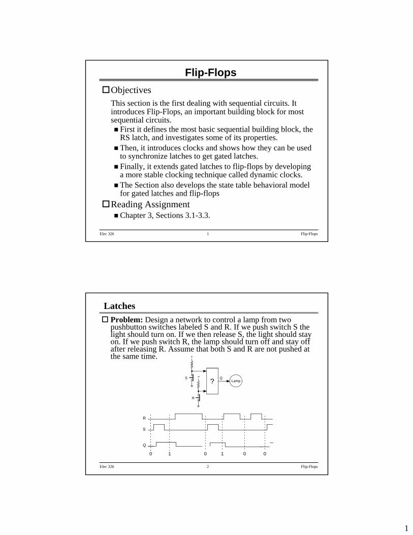
Flip-FlopsObjectivesThis section is the first dealing with sequential circuits. It introduces Flip-Flops, an important building block for most sequential circuits.
First it defines the most basic sequential building block, the RS latch, and investigates some of its properties.Then, it introduces clocks and shows how they can be used to synchronize latches to get gated latches.Finally, it extends gated latches to flip-flops by developing a more stable clocking technique called dynamic clocks.The Section also develops the state table behavioral model for gated latches and flip-flops
Reading Assignment Chapter 3, Sections 3.1-3.3.
2Elec 326 Flip-Flops
LatchesProblem: Design a network to control a lamp from two pushbutton switches labeled S and R. If we push switch S the light should turn on. If we then release S, the light should stay on. If we push switch R, the lamp should turn off and stay off after releasing R. Assume that both S and R are not pushed at the same time. +
Lamp?
R
S Q+
R
S
Q
0 1 0 1 0 0
2
3Elec 326 Flip-Flops
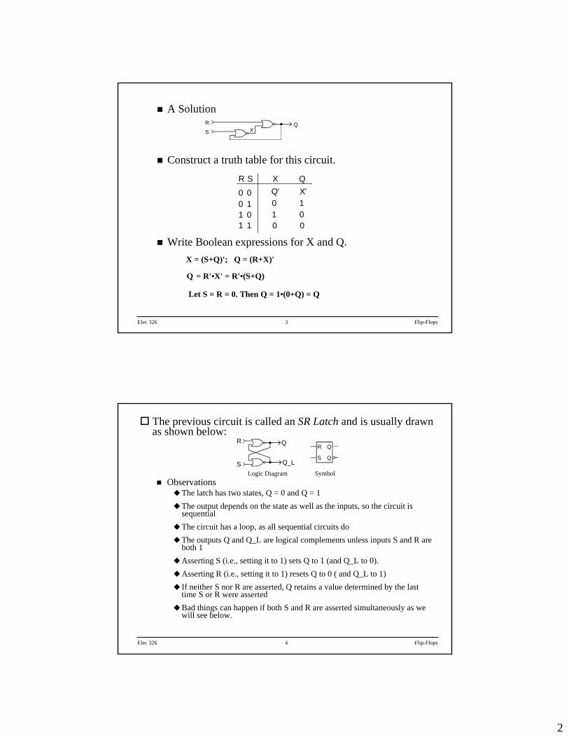
A Solution
Construct a truth table for this circuit.
Write Boolean expressions for X and Q.
R
SQ
X
R S X Q
0 00 11 01 1
0 11 0
X = (S+Q)'; Q = (R+X)'
Q = R'•X' = R'•(S+Q)
Let S = R = 0. Then Q = 1•(0+Q) = Q
0 0
Q’ X’
4Elec 326 Flip-Flops
The previous circuit is called an SR Latch and is usually drawn as shown below:
ObservationsThe latch has two states, Q = 0 and Q = 1The output depends on the state as well as the inputs, so the circuit is sequentialThe circuit has a loop, as all sequential circuits doThe outputs Q and Q_L are logical complements unless inputs S and R are both 1Asserting S (i.e., setting it to 1) sets Q to 1 (and Q_L to 0).Asserting R (i.e., setting it to 1) resets Q to 0 ( and Q_L to 1)If neither S nor R are asserted, Q retains a value determined by the last time S or R were assertedBad things can happen if both S and R are asserted simultaneously as we will see below.
Q
Q_L
R Q
QS
Logic Diagram Symbol
R
S
3
5Elec 326 Flip-Flops
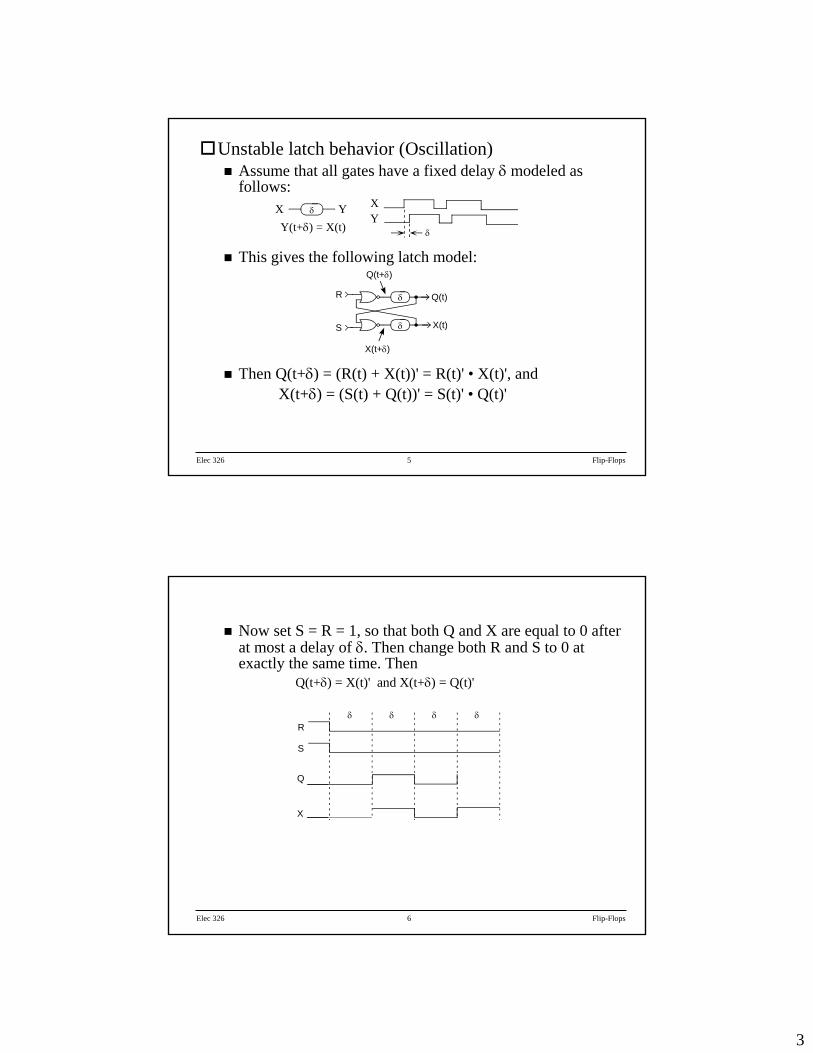
Unstable latch behavior (Oscillation)Assume that all gates have a fixed delay δ modeled as follows:
This gives the following latch model:
Then Q(t+δ) = (R(t) + X(t))' = R(t)' • X(t)', and X(t+δ) = (S(t) + Q(t))' = S(t)' • Q(t)'
δX Y XY
δY(t+δ) = X(t)
δ
Q(t+δ)
δ
X(t+δ)
Q(t)
X(t)
R
S
6Elec 326 Flip-Flops
Now set S = R = 1, so that both Q and X are equal to 0 after at most a delay of δ. Then change both R and S to 0 at exactly the same time. Then
Q(t+δ) = X(t)' and X(t+δ) = Q(t)'
δR
S
Q
X
δ δ δ
4
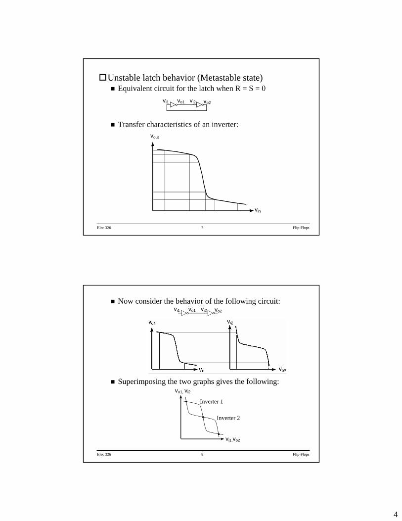
7Elec 326 Flip-Flops
Unstable latch behavior (Metastable state)Equivalent circuit for the latch when R = S = 0
Transfer characteristics of an inverter:
vi1 vo1 vi2 vo2
vout
vin
8Elec 326 Flip-Flops
Now consider the behavior of the following circuit:
Superimposing the two graphs gives the following:
Inverter 1
Inverter 2
vi1,vo2
vo1, vi2
vi1 vo1 vi2 vo2
5
9Elec 326 Flip-Flops
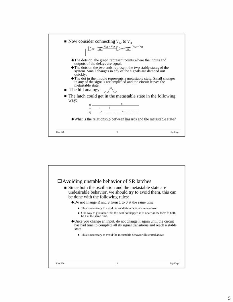
Now consider connecting v02 to vi1
The dots on the graph represent points where the inputs and outputs of the delays are equal. The dots on the two ends represent the two stable states of the system. Small changes in any of the signals are damped out quickly.The dot in the middle represents a metastable state. Small changes in any of the signals are amplified and the circuit leaves the metastable state.
The hill analogy: The latch could get in the metastable state in the following way:
What is the relationship between hazards and the metastable state?
vo1 = vi2δ δ
vo2 = vi1
RS
Q
10Elec 326 Flip-Flops
Avoiding unstable behavior of SR latchesSince both the oscillation and the metastable state are undesirable behavior, we should try to avoid them. this can be done with the following rules:
Do not change R and S from 1 to 0 at the same time. This is necessary to avoid the oscillation behavior seen aboveOne way to guarantee that this will not happen is to never allow them to both be 1 at the same time.
Once you change an input, do not change it again until the circuit has had time to complete all its signal transitions and reach a stable state.
This is necessary to avoid the metastable behavior illustrated above
6
11Elec 326 Flip-Flops
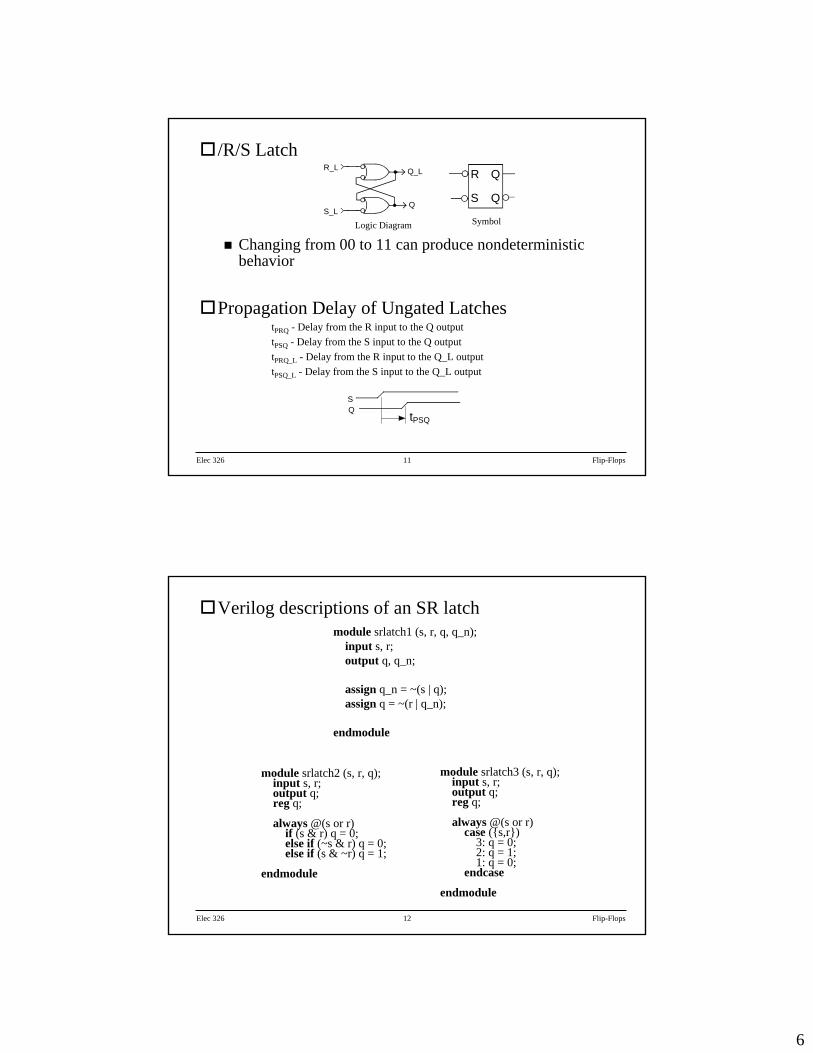
/R/S Latch
Changing from 00 to 11 can produce nondeterministic behavior
Propagation Delay of Ungated LatchestPRQ - Delay from the R input to the Q outputtPSQ - Delay from the S input to the Q outputtPRQ_L - Delay from the R input to the Q_L outputtPSQ_L - Delay from the S input to the Q_L output
SQ
tPSQ
R_L
S_L
Q_L
Q
R Q
QS
SymbolLogic Diagram
12Elec 326 Flip-Flops
Verilog descriptions of an SR latchmodule srlatch1 (s, r, q, q_n);
input s, r;output q, q_n;
assign q_n = ~(s | q);assign q = ~(r | q_n);
endmodule
module srlatch2 (s, r, q);input s, r;output q;reg q;
always @(s or r)if (s & r) q = 0;else if (~s & r) q = 0;else if (s & ~r) q = 1;
endmodule
module srlatch3 (s, r, q);input s, r;output q;reg q;
always @(s or r)case ({s,r})
3: q = 0;2: q = 1;1: q = 0;
endcase
endmodule
7
13Elec 326 Flip-Flops
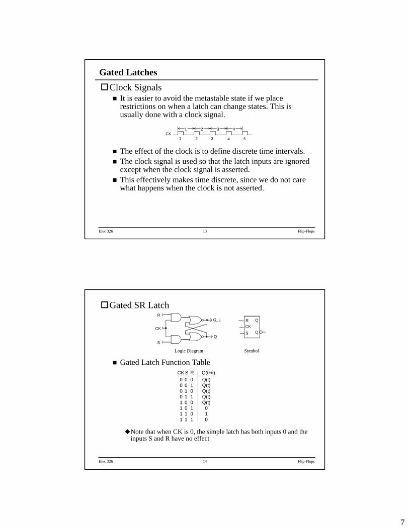
Gated LatchesClock Signals
It is easier to avoid the metastable state if we place restrictions on when a latch can change states. This is usually done with a clock signal.
The effect of the clock is to define discrete time intervals.The clock signal is used so that the latch inputs are ignored except when the clock signal is asserted. This effectively makes time discrete, since we do not care what happens when the clock is not asserted.
1
1
2 3 4
2 3 4 5CK
14Elec 326 Flip-Flops
Gated SR Latch
Gated Latch Function Table
Note that when CK is 0, the simple latch has both inputs 0 and the inputs S and R have no effect
R
S
Q_L
Q
R Q
QS
SymbolLogic Diagram
CK CK
00001111
00110011
01010101
Q(t)Q(t)Q(t)Q(t)Q(t)
010
S RCK Q(t+δ)
8
15Elec 326 Flip-Flops
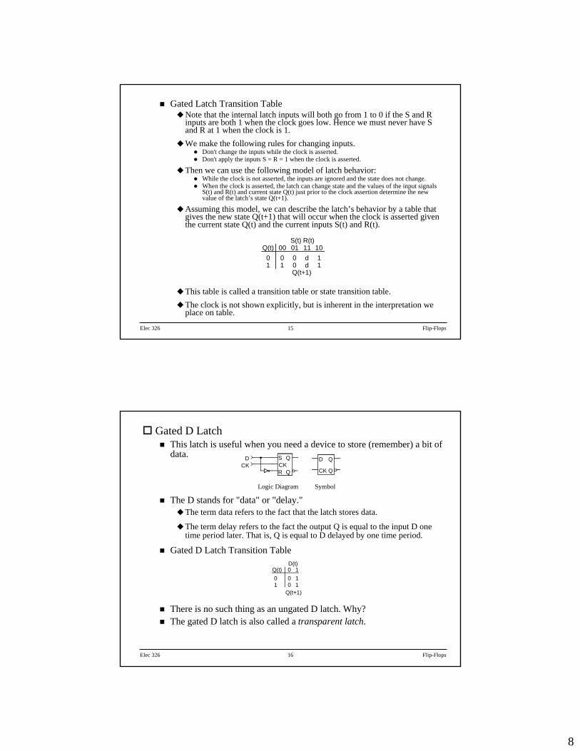
Gated Latch Transition TableNote that the internal latch inputs will both go from 1 to 0 if the S and R inputs are both 1 when the clock goes low. Hence we must never have S and R at 1 when the clock is 1. We make the following rules for changing inputs.
Don't change the inputs while the clock is asserted.Don't apply the inputs S = R = 1 when the clock is asserted.
Then we can use the following model of latch behavior:While the clock is not asserted, the inputs are ignored and the state does not change.When the clock is asserted, the latch can change state and the values of the input signals S(t) and R(t) and current state Q(t) just prior to the clock assertion determine the new value of the latch’s state Q(t+1).
Assuming this model, we can describe the latch’s behavior by a table that gives the new state Q(t+1) that will occur when the clock is asserted given the current state Q(t) and the current inputs S(t) and R(t).
This table is called a transition table or state transition table.The clock is not shown explicitly, but is inherent in the interpretation we place on table.
01
01
00
dd
11
S(t) R(t)00 01 11 10Q(t)
Q(t+1)
16Elec 326 Flip-Flops
Gated D LatchThis latch is useful when you need a device to store (remember) a bit of data.
The D stands for "data" or "delay." The term data refers to the fact that the latch stores data.
The term delay refers to the fact the output Q is equal to the input D one time period later. That is, Q is equal to D delayed by one time period.
Gated D Latch Transition Table
There is no such thing as an ungated D latch. Why?The gated D latch is also called a transparent latch.
CKD
R
Q
Q
SCK
D Q
QCK
SymbolLogic Diagram
01
00
Q(t)D(t)
Q(t+1)
11
0 1
9
17Elec 326 Flip-Flops
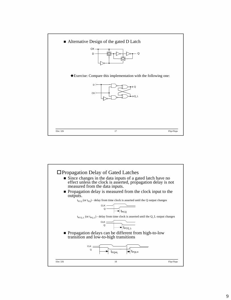
Alternative Design of the gated D Latch
Exercise: Compare this implementation with the following one:
D
Q_L
Q
CK
CK
D Q
18Elec 326 Flip-Flops
Propagation Delay of Gated LatchesSince changes in the data inputs of a gated latch have no effect unless the clock is asserted, propagation delay is not measured from the data inputs.Propagation delay is measured from the clock input to the outputs.
tPCQ (or tPQ) - delay from time clock is asserted until the Q output changes
tPCQ_L (or tPQ_L) - delay from time clock is asserted until the Q_L output changes
Propagation delays can be different from high-to-low transition and low-to-high transitions
CLKQ
tPCQ
CLKQ
tPCQ_L
CLKQ
tPQHL tPQLH
10
19Elec 326 Flip-Flops
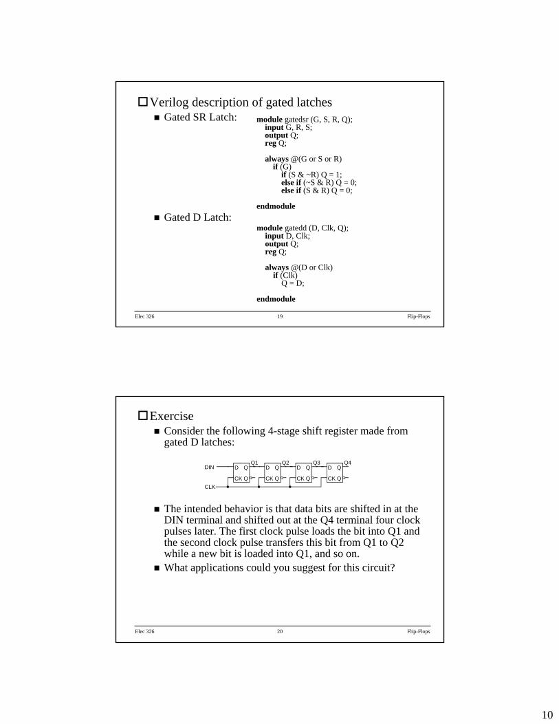
Verilog description of gated latchesGated SR Latch:
Gated D Latch:module gatedd (D, Clk, Q);
input D, Clk;output Q;reg Q;
always @(D or Clk)if (Clk)
Q = D;
endmodule
module gatedsr (G, S, R, Q);input G, R, S;output Q;reg Q;
always @(G or S or R)if (G)
if (S & ~R) Q = 1;else if (~S & R) Q = 0;else if (S & R) Q = 0;
endmodule
20Elec 326 Flip-Flops
ExerciseConsider the following 4-stage shift register made from gated D latches:
The intended behavior is that data bits are shifted in at the DIN terminal and shifted out at the Q4 terminal four clock pulses later. The first clock pulse loads the bit into Q1 and the second clock pulse transfers this bit from Q1 to Q2 while a new bit is loaded into Q1, and so on.What applications could you suggest for this circuit?
D Q
QCK
DIN
CLK
Q1 Q2 Q3 Q4D Q
QCK
D Q
QCK
D Q
QCK
11
21Elec 326 Flip-Flops
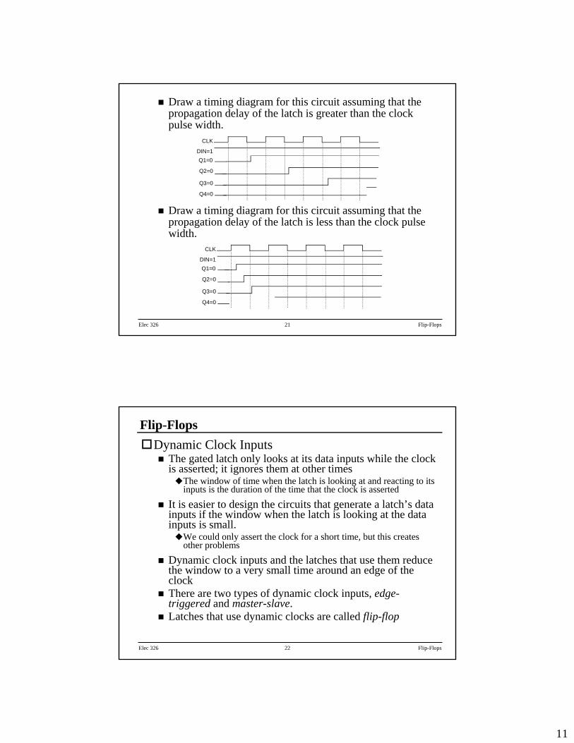
Draw a timing diagram for this circuit assuming that the propagation delay of the latch is greater than the clock pulse width.
Draw a timing diagram for this circuit assuming that the propagation delay of the latch is less than the clock pulse width.
CLK
Q1=0
Q2=0
DIN=1
Q3=0
Q4=0
CLK
Q1=0
Q2=0
DIN=1
Q3=0
Q4=0
22Elec 326 Flip-Flops
Flip-FlopsDynamic Clock Inputs
The gated latch only looks at its data inputs while the clock is asserted; it ignores them at other times
The window of time when the latch is looking at and reacting to its inputs is the duration of the time that the clock is asserted
It is easier to design the circuits that generate a latch’s datainputs if the window when the latch is looking at the data inputs is small.
We could only assert the clock for a short time, but this creates other problems
Dynamic clock inputs and the latches that use them reduce the window to a very small time around an edge of the clockThere are two types of dynamic clock inputs, edge-triggered and master-slave.Latches that use dynamic clocks are called flip-flop
12
23Elec 326 Flip-Flops
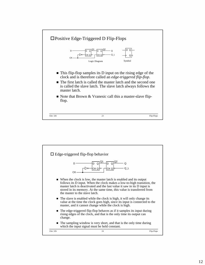
Positive Edge-Triggered D Flip-Flops
This flip-flop samples its D input on the rising edge of the clock and is therefore called an edge-triggered flip-flop.The first latch is called the master latch and the second one is called the slave latch. The slave latch always follows the master latch.Note that Brown & Vranesic call this a master-slave flip-flop.
D
CK
Q1 Q2D Q
QCK
D Q
QCK
Q
Q_L
D Q
Q
SymbolLogic Diagram
24Elec 326 Flip-Flops
Edge-triggered flip-flop behavior
When the clock is low, the master latch is enabled and its output follows its D input. When the clock makes a low-to-high transition, the master latch is deactivated and the last value it saw in its D input is stored in its memory. At the same time, this value is transferred from the master to the slave latch.The slave is enabled while the clock is high, it will only change its value at the time the clock goes high, since its input is connected to the master, and it cannot change while the clock is high.The edge-triggered flip-flop behaves as if it samples its input during rising edges of the clock, and that is the only time its output can change. The sampling window is very short, and that is the only time during which the input signal must be held constant.
D
CK
Q1 Q2D Q
QCK
D Q
QCK
Q
Q_L

13
25Elec 326 Flip-Flops
Negative Edge-Triggered D Flip-Flops
Asynchronous Inputs
If CLK is held at 0, the D flip-flop acts like an SR latch with PR the set input and CLR the reset input
D
CK
Q1 Q2D Q
QCK
D Q
QCK
Q
Q_L
D Q
Q
PR
CLR
R Q
QS
R Q
QS
CLR_L
PR_LCK
D Q
Q_L
Logic Diagram Symbol
26Elec 326 Flip-Flops
Edge-Triggered JK Flip-FlopsThe JK Flip-Flop has two inputs J and K. All four possible input configurations are valid. The J acts like S and the K acts like R, when there is only one input with value 1. When both J and K are 1, the flip-flop toggles.
What would happen if we used a gated D latch instead of an edge triggered flip-flop?
0
1
0
1
0
0
1
0
1
1
00 01 11 10JK
Q
Q*Q* = J•Q’ + K’•Q
D Q
Q
J
CKK Q
Q_L

14
27Elec 326 Flip-Flops
Verilog descriptions of edge-triggered flip-flopsD Flip-Flop
JK Flip-Flop
module flipflopd (D, Ck, Clr, Q);input D, Ck, Clr;output Q;reg Q;
always @(posedge Ck or posedge Clr)if (Clr) Q = 0;else Q = D;
endmodule
module flipflopjk (Ck, J, K, Q);input Ck, J, K;output Q;reg Q;
always @(negedge Ck)if (J & ~K) Q = 1;else if (~J & K) Q = 0;else if (J & K) Q = ~Q;
endmodule
28Elec 326 Flip-Flops
Timing parameters for edge-triggered flip-flopsInputs must not change while they are being sampled by the clock.
Setup and hold times
Propagation delays
Propagation delay must exceed hold time!
SamplingWindow
tsu thCK
tsu - Setup timeth - Hold time
CK
Q
tPLH(CQ) tPHL(CQ)
CK
QD
tP
th
15
29Elec 326 Flip-Flops
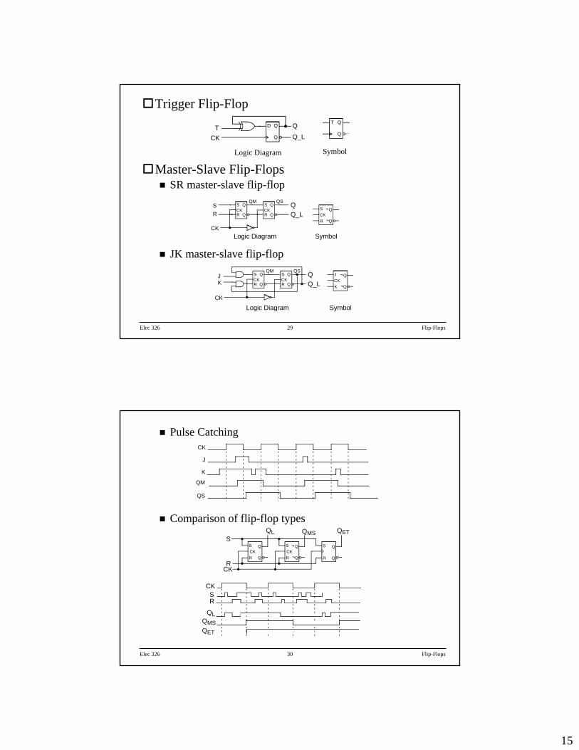
Trigger Flip-Flop
Master-Slave Flip-FlopsSR master-slave flip-flop
JK master-slave flip-flop
D Q
Q
TCK
QQ_L
T Q
Q
Logic Diagram Symbol
S Q
QRCK
S Q
QRCK
SR
CK
QQ_L
QM QSS Q
QRCK
Logic Diagram Symbol
S Q
QRCK
S Q
QRCK
JK
CK
QQ_L
QM QSJ Q
QKCK
SymbolLogic Diagram
30Elec 326 Flip-Flops
Pulse Catching
Comparison of flip-flop types
CK
J
K
QM
QS
S Q
QRCK
S Q
QRCK
S Q
QR
S
RCK
QL QMS QET
QLQMSQET
CKSR
16
31Elec 326 Flip-Flops
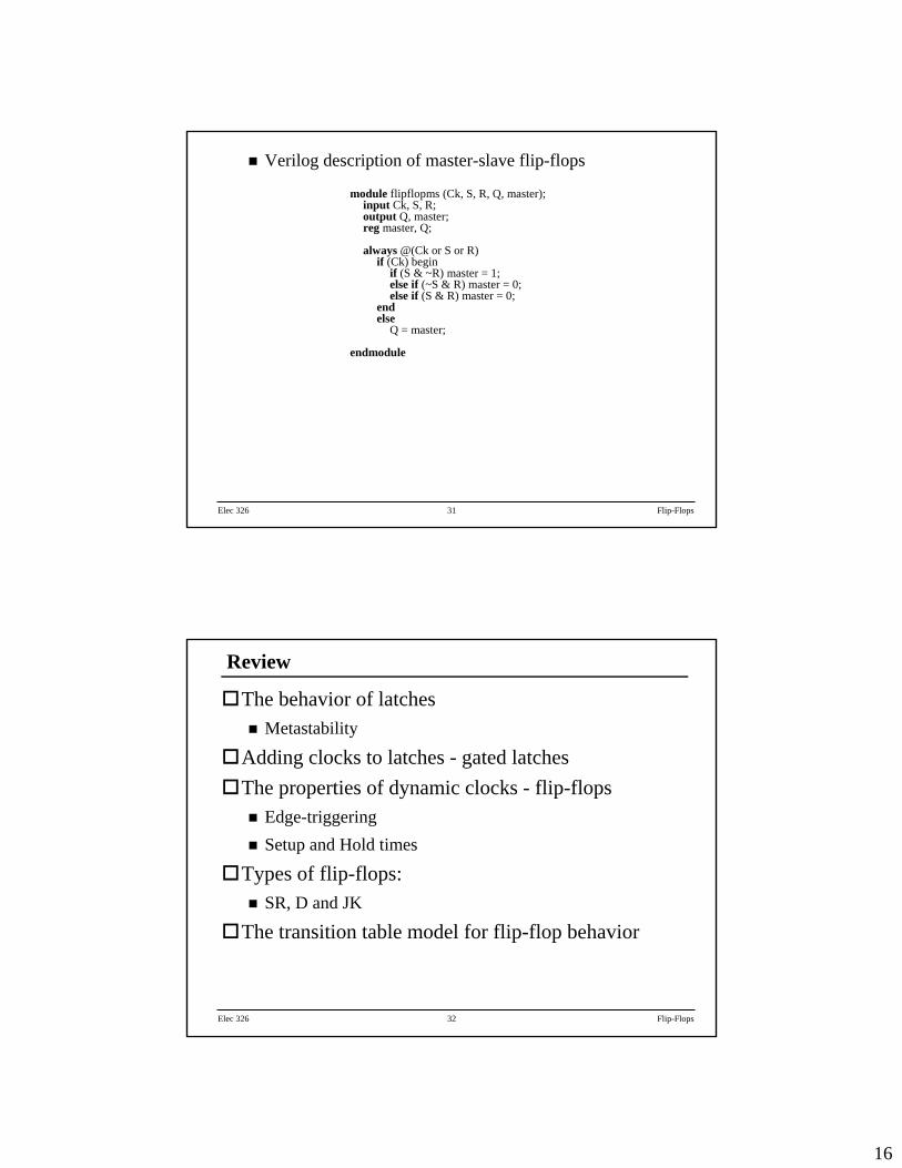
Verilog description of master-slave flip-flops
module flipflopms (Ck, S, R, Q, master);input Ck, S, R;output Q, master;reg master, Q;
always @(Ck or S or R)if (Ck) begin
if (S & ~R) master = 1;else if (~S & R) master = 0;else if (S & R) master = 0;
endelse
Q = master;
endmodule
32Elec 326 Flip-Flops
Review
The behavior of latchesMetastability
Adding clocks to latches - gated latchesThe properties of dynamic clocks - flip-flops
Edge-triggeringSetup and Hold times
Types of flip-flops:SR, D and JK
The transition table model for flip-flop behavior