Rensselaer Polytechnic Institute · Web viewBACKGROUND THEORY Boolean Algebra Switching Algebra...
29
Rensselaer Polytechnic Institute ECSE-4760 Real-Time Applications in Control & Communications EXPERIMENTS IN DIGITAL LOGIC DESIGN Number of Sessions – 4 INTRODUCTION Over the past few decades the digital world has come into its own. Even though engineering has gone into specialization, it is necessary to understand digital circuits to be able to communicate with others. This experiment attempts to teach a simple method of designing digital circuits. Due to the quick pace of the lab, it is highly recommended that you read one of the references. This will enable you to proceed quickly through the preliminary problems so you will have more time for the design problems. The following is an outline of the experiment. Following each section will be a set of questions that should be answered to show an understanding of the material presented. Any difficulties should be referred to a reference or your instructor. You should use the DesignWorks (LogicWorks or any other you may have) logic circuit simulator on the Macintosh after most sections to cement together all the preceding sections. BACKGROUND THEORY Boolean Algebra Switching Algebra Combinational Logic Minimization Flip-Flops and Registers Counters Synthesis of Synchronous Circuits 1
Transcript of Rensselaer Polytechnic Institute · Web viewBACKGROUND THEORY Boolean Algebra Switching Algebra...

Rensselaer Polytechnic Institute
ECSE-4760Real-Time Applications in Control &
Communications
EXPERIMENTS IN DIGITAL LOGIC DESIGN
Number of Sessions – 4
INTRODUCTION
Over the past few decades the digital world has come into its own. Even though engineering has gone into specialization, it is necessary to understand digital circuits to be able to communicate with others. This experiment attempts to teach a simple method of designing digital circuits.
Due to the quick pace of the lab, it is highly recommended that you read one of the references. This will enable you to proceed quickly through the preliminary problems so you will have more time for the design problems.
The following is an outline of the experiment. Following each section will be a set of questions that should be answered to show an understanding of the material presented. Any difficulties should be referred to a reference or your instructor. You should use the DesignWorks (LogicWorks or any other you may have) logic circuit simulator on the Macintosh after most sections to cement together all the preceding sections.
BACKGROUND THEORYBoolean AlgebraSwitching AlgebraCombinational LogicMinimizationFlip-Flops and RegistersCountersSynthesis of Synchronous Circuits
EXPERIMENTAL PROCEDUREQuestions and ProblemsSimulator Operation & FPGA Implementation
REFERENCES
It is required that you show all circuits, as built, in your write-up. Please include equations too. The first part of the procedure section contains all the questions and problems to be
1

answered and the second part describes the use of DesignWorks. Note: all references to DesignWorks (on Macintosh computers) throughout this procedure may be replaced with LogicWorks on the lab Windows PCs.BACKGROUND THEORY
Since the digital world consists of discrete levels, functions can be described in truth tables as opposed equations for the continuous world. The three basic digital functions are AND, OR, and NOT. Their symbols and truth tables are shown below. These functions (from now on called gates) are such that as soon as the inputs change, the outputs will also change. (There actually is a small delay dependent on the type of gate. See reference [1].)
FIGURE 1. AND gate and truth table.
FIGURE 2. OR gate and truth table.
FIGURE 3. NOT gate and truth table.
Very often an OR and AND gate will have a NOT at the end of it (because of hardware considerations). These will then be called NOR and NAND gates respectively.
Please do problem 1 in the QUESTIONS AND PROBLEMS of the EXPERIMENTAL PROCEDURE.
BOOLEAN ALGEBRA
George Boole (1815-64) introduced an algebra of logic in the mid-1800's, however, the present-day application of Boolean algebra is credited to a paper by C. Shannon in 1938. The techniques and manipulations provided by Boolean Algebra are a necessity to efficient logic design.
A. Definition
2

A set of elements B and two binary operations '+' and '·' over B form a Boolean Algebra {B, +, ·} if and only if the following postulates hold:
Postulate 1 - The set of B objects or elements are subject to an equivalence relationship, denoted '=', which satisfies the principle of substitution, i.e., if A = B, A may be substituted for B in any expression involving B without affecting the validity of the expression. As in ordinary algebra, the letters of the alphabet are used to represent variables.Postulate 2 (Closure) - Whenever A, B B then
(A + B) B(A · B) B
Postulate 3 (Identity) - There exist two identity elements (called 0 and 1) such that:0 + A = A + 0 = A (additive identity)
1 · A = A · 1 = A (multiplicative identity)Postulate 4 - '+' and '·' are:
i. commutativeA + B = B + AA · B = B · A
ii. associativeA + (B + C) = (A + B) + C
A · (B · C) = (A · B) · Ciii. distributive over each other
A · (B + C) = (A · B) + (A · C)A + (B · C) = (A + B) · (A + C)
Postulate 5 - For every element A in B there exists an element A (termed the complement of A) such that:
A+ A=1A⋅A=0
Postulate 6 - There are at least two elements X and Y in B such that X ≠ Y.
B. Theorems
1. The 0 and 1 elements are unique.2. For every element A in B: A + A = A and A · A = A3. A + 1 = 1 and A · 0 = 04. The elements 0 and 1 are distinct and 1=0 or 0=1 .5. A + AB = A and A · (A + B) = A. This is often termed the absorption rule. (The '·' is understood, thus A · B = AB)6. A=( A )= ¯A
7. A+ A B=A+B and A⋅( A+B)=AB
8. ( A+B)⋅( A+C )=AC+ A B and AB+BC+ A C=AB+ A C9. DeMorgan's Theorem
AB= A+ BA+B= A⋅B
C. Duality
Notice that the previous postulates and theorems were given in pairs. In each case one postulate in a pair can be obtained from the other by interchanging 0 and 1 along with '+' and '·'. This is called the principle of duality. Every theorem which can be proven for Boolean algebra has a dual which is also true. For example:
A + 0 = AA · 1 = A
3

andA + (B · C) = (A + B) · (A + C)A · (B + C) = (A · B) + (A · C)
SWITCHING ALGEBRA
Switching algebra is a mathematical framework for the design and analysis of logic networks using binary decision-making elements such as NAND and NOR gates. The distinctive feature is that variables and functions can assume only two values, 0 and 1. Thus Switching algebra is a subset of Boolean algebra restricted to two elements (B = 0, 1). Switching algebra will provide a means of describing functional relationships in a form that corresponds precisely to a network of gates.
A. Properties of Switching Algebra
1. Distinctness of 0 and 1X ≠ 0 if and only if X = 1X ≠ 1 if and only if X = 0
2. OperationsAND, '·'
0 · 0 = 00 · 1 = 1 · 0 = 01 · 1 = 1
OR, '+'0 + 0 = 00 + 1 = 1 + 0 = 11 + 1 = 1
NOT, '¯¯ '1=00=1
The associative law allows us to extend definitions of AND and OR to many variables. Thus for Z = A + B + C + D + E, then Z = 1 if any of A, B, C, D, or E is 1, in any combination. Similarly Z = ABCDE is 1 if and only if all the variables A, B, C, D, and E are 1.
B. DeMorgan's Theorem
The two basic duals of the theorem are:XY =X+YX+Y =X⋅Y
DeMorgan's theorem as well as other theorems can be extended to many variables:ABCDE . ..=A+ B+C+D+ E+.. .A+B+C+.. .= A⋅B⋅C⋅.. .
DeMorgan's theorem expresses a relationship between AND and OR that is important to recognize. Consider the equation Z = A + B + C. We could interpret this as Z = 1 when A or B or C is 1. An alternative is Z = 0 if A and B and C are 0. This is represented by Z= A⋅B⋅C which is equivalent to Z = A + B + C by DeMorgan's theorem.
All this leads to the need to realize that a gate can be realized by its dual using DeMorgan's theorem. Some examples are as follows:
4

FIGURE 4.It is important to note that AB and A⋅B are not equivalent expressions. The truth table
for both is shown below.
FIGURE 5.
Answer question 2 in the QUESTIONS AND PROBLEMS of the EXPERIMENTAL PROCEDURE.
COMBINATIONAL LOGIC
Combinational logic refers to networks whose outputs depend solely on their inputs, and not on any previous state. The analysis of combinational logic requires the writing of the Boolean algebra equation for each element of the network, and then combining these for the final output equation. For example:
E1=ABCE2=A BCE3=E1+E2F=ABC +A B C
FIGURE 6.
The truth table is:
5

FIGURE 7.
DeMorgan's theorem states that AB= A+ B . Therefore a NAND gate is also a NOT OR gate, as shown below.
F1=AB F2= A+BFIGURE 8.
When analyzing NAND circuits, a NOTed-OR can be substituted in place of a NAND gate. This is usually done at odd levels as shown below.
E1=ABE2=CDF1=AB CD=AB+CD=F2
FIGURE 9.
NAND gates are used mainly for the simplicity of their hardware components. Analysis of NOR circuits follows similar reasoning.
Synthesis of combinational logic is just the reverse of analysis. Implement each section of a Boolean equation and then OR or AND the sections together to get the final output. For example, implement F=A B+ ACD using NAND logic.
6

E1=A BE2=ACDF=A B+ ACD
FIGURE 10.
Implement F=AB+ D(B+C )
E1=ABE2=B+CE3=D( B+C )F=AB+ D(B+C )
FIGURE 11.
Sum of Products, Products of Sums
There are two basic forms in which a Boolean algebraic expression can be written. These are the sum of products (SOP) and the product of sums (POS). That is, the expression AB+ A B is an ORing of the two ANDed terms. The ANDed terms, AB and A B , are called product terms. The ORing is the sum of the terms. Therefore, the above expression is a sum of products. Likewise, a product of sums expression could be ( A+B)( A+ B ).
Answer question 3 in the QUESTIONS AND PROBLEMS of the EXPERIMENTAL PROCEDURE.
MINIMIZATION
Algebra theorems provide the fundamental tools of minimization. Reduction such as A+ A B=A+B are easily recognized while others, such as A B+B C+ A C , are not as obvious. For example, reduce F=A B C+ A B C+B+ B D by algebraic manipulation
F=BC ( A+ A )+B+ B D=B C+B+D=B+C+D
ReduceF=A B+ B C+ A C=A B+( A+ A ) BC + A C=A B+ A BC+ A BC+ A C=A B(1+C )+ A C( B+1 )=A B+ A C
Algebraic reduction of Boolean functions is not easy and requires considerable experience, judgment, and luck. This becomes more apparent as the complexity of the
7

function increases. As a result, the use of Karnaugh Maps, which is a powerful tool in minimizing logic, will be taught.
A. Karnaugh Maps
Each variable can exist as either of two values; 0 and 1. Two squares can represent this.
FIGURE 12.
Similarly, two variables can be described as follows:
FIGURE 13.
Thus A=1, A=0 , B=1 , B=0 . The map then looks as follows:
BA 0 10 A B A B1 A B AB
FIGURE 14.
The two combinations of A are listed on top, and the two combinations of B are listed on the side. The intersections form the four unique combinations of the two variables.
The K-map representation is constructed by placing a 1 in any cell for which the function of the variables is 1. Therefore the function F= A B+ AB can be mapped as:
BA 0 10 1 01 0 1
FIGURE 15.
The way of minimizing algebra can be easily seen by the function F=A B+ AB=A
BA 0 10 0 01 1 1
FIGURE 16.
It can be obviously seen from the map that when A = 1, F = 1 regardless of the value of B. It is this property, of visually recognizing two adjacent ones, that makes K-maps such a
8
F= A B+ AB
F=A B+ AB

powerful tool. Although the 2-variable problem is trivial, K-maps can be extended to 3, 4, and more variables.
FIGURE 17. Methods of representing 3 and 4 variable maps.
B. Minimum Sum of Products
There are two rules. The first is to order the variables so that only one variable changes at a time (see FIGURE 17). This is important because when two adjacent 1 valued cells are paired, only one variable changes and that is the redundant variable.
The second rule is to group the 1's in the largest power of two possible. This way one, two, or more variables can be seen as redundant. For example, F= A B C D+ A B C D+ ABC { D+ A BCD+ A B C D+ A BC { D¿+ A B C D ¿ can be minimized as follows.
FIGURE 18.
By pairing 1's, F reduces to BC D+ A C D+AC { D+ A BC ¿ . Notice that groups can be extended off the edge of the map. Continuing by trying to group the largest power of two takes the following form.
FIGURE 19.
The function is now F=C D+ B D+ A BC . Notice how the four corners combine. This may seem odd, but if the map is enlarged (adding no new information), this will become obvious.
9

FIGURE 20.
There are times when you have a choice in covering (drawing circles around) the 1's. In this case you pick the coverage that suits other parameters. For example,
CD AB 00 01 11 10
00 1 1 F=A B D+BD+ A C D01 1 1 1 or11 1 1 F=A B D+BD+ A BC10
FIGURE 21.
To include both covers would add a redundant term to F.
In summary, to minimize the terms of a function, get the fewest covers, covering the largest area possible. As a closing note, sometimes there will arise a switching application that will not contain all the possible values needed to fill a K-map. In this condition, you don't really care if a cell is zero or one. Therefore it is correct to cover the largest possible area including don't care's. For example,
CD AB 00 01 11 10
00 1 d 1 101 0 0 0 0 d = don’t care11 d 0 1 1 F=A B+AC10 0 0 1 d
FIGURE 22.
Answer question 4 in the QUESTIONS AND PROBLEMS of the EXPERIMENTAL PROCEDURE.
FLIP-FLOPS AND REGISTERS
One of the most common types of memory is the flip-flop (otherwise known as the bistable multivibrator). The four we will be concerned about are S-R, J-K, T, and D. The
10

characteristics of each of the flip-flops will be covered in this section. The C input is the clock input used in some flip-flops to synchronize transitions.
A. S-R Flip-Flop (LATCH)
FIGURE 23 shows the logic circuit for the flip-flop constructed with two NAND gates. Also shown are the symbol and operation table. Note that the output Q is not necessarily the complement of Q.
FIGURE 23. Latch.
As can be seen, the outputs are uniquely determined by the inputs except for the (1,1) condition where the output stays at its previous state. Problems occur when the inputs switch from (0,0) to (1,1) simultaneously. In the real world there would be a race between the gates.
B. J-K Flip-Flop
FIGURE 24 shows the symbol and operation table for a J-K flip-flop.
FIGURE 24. J-K flip-flop.
C. D Flip-Flop
FIGURE 25 shows the symbol and operation table for a D flip-flop. As can be seen, it is easily constructed from a J-K flip-flop.
11

FIGURE 25. D flip-flop.
The D flip-flop will simply assume the state of the input after a clock pulse. This is useful as a delay element and when transferring bits from one source to another. The D flip-flop is commonly used in shift registers.
D. T Flip-Flop
FIGURE 26 describes the T flip-flop. As shown, the T flip-flop is simply a J-K flip-flop with the two inputs connected. It is commonly used in counters.
FIGURE 26. T flip-flop.
E. Shift Registers
Shift registers occupy an important position in most digital systems. They are often used to momentarily store binary information needed to be coded or decoded. They also play an important link between systems using sequential I/O channels.
The flip-flops in a register must be wired so binary data can be inserted (shifted) into the register, and probably shifted out as well.
F. Serial Shift Registers
Serial shift registers involve shifting bits into the register one at a time in a series fashion. A five bit serial shift register is shown below using D flip-flops. Data shifts from a flip-flop to the next one to its right, on each clock pulse.
12

FIGURE 27. Serial shift register.
Data can be taken out in a parallel or serial fashion, as shown.
G. Parallel Load Shift Registers
A second method of loading a register is by shifting in all the bits in parallel at the same time (for example from a decoder). An example of a 3-bit parallel shift register is shown below.
FIGURE 28.
When the shift line goes high, the outputs of the AND gates take on the values of X. On the next clock, this information is shifted into the register. To reset the register, the reset line goes high and the shift line low so that all the Q's will turn low on the next clock pulse. Thus this configuration requires two clock pulses; one to reset and one to load.
Probably the most useful register is a parallel load, serial shift register that lets you control either mode. That type of register incorporates the two previous techniques.
Answer question 5 in the QUESTIONS AND PROBLEMS of the EXPERIMENTAL PROCEDURE.COUNTERS
Only synchronous counters will be described because of their simplicity. A synchronous counter is one in which all the flip-flops change state simultaneously since all the clocks inputs are tied together. Counters are usually constructed of T flip-flops since the flip-flops only have to toggle at a given sequence. A 3-bit synchronous counter is shown below.
13

FIGURE 29. 3-Bit synchronous counter.
The equations for the flip-flops are T1 = 1; T2 = Q1; T3 = Q1 · Q2. Thus T1 toggles at every clock pulse, T2 toggles only when Q1 is high, on every other clock pulse, and finally T3 toggles when both Q1 and Q2 are high, or every fourth clock pulse. The counting sequence is shown below:
FIGURE 30. Counting sequence.
This type of counter can be extended by the following set of equations.T1 = 1T2 = T1T3 = T1T2Tn = T1T2…Tn-1
Counter Designs
The 'Detect and Steer' method works by constructing the appropriate combinational control logic at the input of each flip-flop so that the counter progresses through the desired states. A list of general steps used to design a counter by this method is shown below.
1. Start by writing the desired counting sequence.2. From 1 determine which flip-flop must change when going from the last state to the
first.3. Generate the control circuitry for each flip-flop from the analysis done in 2.
14

4. This can best be shown by the following design of a Mod-11 synchronous binary counter.
FIGURE 31.
To find the expression for the T flip-flop inputs, note that there are several unused states that will add don’t cares to the K-map. These are ABCD = 1011, 1100, 1101, 1110 & 1111. For the T4 input for A, this flip-flop should change (T4 = 1) when ABCD = 0111 & 1010. The K-map with the don’t cares will be:
CD AB 00 01 11 10
0001 1 d = don’t care11 d d d d T4 = BCD + AC10 d 1
Similarly, T3 for B needs to be 1 when ABCD = 0011 & 0111. The corresponding K-map is:
CD AB 00 01 11 10
00 1
01 1 d = don’t care11 d d d d T3 = CD10 d
15

You should work out the expression for C’s T2 flip-flop, noting that there will be six 1s in the K-map. The T1 expression for D could also be done this way, but since D changes almost every time, it is easier to look at the case when it doesn’t change. Instead of filling up the K-map with all 1s except for the lower right corner, we will put a 0 in for the ABCD = 1010 state and find the inverse (NOT) expression. Now the K-map will look like:
CD AB 00 01 11 10
00 1 1 1 101 1 1 1 1 d = don’t care11 d d d d T1 = AC10 1 1 d 0
Once we detect the 1010 state for D (detecting AC) we can summarize all the T flip-flop input expressions:
D = T1 = A⋅C inhibits only on A · C; otherwise 1C = T2 = D + A · C A · C is the force termB = T3 = C · DA = T4 = B · C · D + A · C A · C is the force term
The logic for the Mod-11 counter is shown below:
FIGURE 32.
Answer question 6 in the QUESTIONS AND PROBLEMS of the EXPERIMENTAL PROCEDURE.
SYNTHESIS OF SYNCHRONOUS CIRCUITS (see Ref. [2])
The synthesis of a logic circuit is one of the most difficult aspects of digital circuit design. The designer must balance the cost of his time spent on the design to the cost of the logic used. (This really applies to prototypes. For production, the designer will be more interested in minimizing his circuit than minimizing his time.) There is a method, which will be explained, that minimizes the designer's time spent working out his circuit, and maximizes his time where thought process is needed – flow-charting.
Flow-charting is used everywhere. In composition it is called an outline. Programmers use it. In flow-charting a finite state machine, the designer takes all the specs and puts it into his flow chart.
Let's take a simple example - the design of a Mod-8 counter. You already know how to design T-FF counters. This time we will synthesize a D-FF counter. Since 8 distinct outputs
16

are needed, the design calls for 8 states since each output will depend on the state you are in. The flow chart is as follows:
FIGURE 33.
Each state is represented by a circled letter. The arrow points to the next state following a clock pulse. For a simple counter, the arrows just follow a string. The number following the slash shows the desired output at each transition. If there was an input it would be put in front of the slash.
Let's continue. Suppose we wanted an up/down counter dependent upon an input, X. When X = 1 the counter counts up and for X = 0 the counter counts down. The implementation of this flow chart is just as simple. We now have arrows in both directions, dependent on X.
FIGURE 34.
On X (when X=0 ) the arrows point backwards. The outputs follow similar reasoning.
Now for a final extension. The new design calls for two inputs X,Y. On 0,1 you have a down counter; on 1,0 you have an up counter; and on 0,0 and 1,1 you stop counting. Only the first 4 states will be shown.
FIGURE 35.
Once a good working flow chart has been accomplished (minimization will not be covered) the rest is pure mechanics. The step after the flow chart is to write a state table. Let's work on a simple 4 state up/down counter. This table simply lists each state on the left, and the transition to the next state inside the box, dependent on the input variable X. From the state table, an excitation table is written. Using K-map techniques, a state representation is made and inserted for each state. Notice that only one variable changes at a time when using a K-map. Using K-map techniques, the equations for each flip-flop are found. Note that Q1Q2 are the outputs of flip-flops. The digits inside the box are for the inputs of the flip-flops.
17

X0 1
XQ1Q2 0 1
A D B (A) 00
11 01
B A C (B) 01
00 10
C B D (C) 11
01 11
D C A (D) 10
10 00
State Table Excitation Table Excitation EquationsFIGURE 36.
Going back to the flow chart, an output table is written. It may seem a little odd that each state codes for two outputs, but you must realize that the coding is for the next state, not the immediate state. Finally, the equations for the outputs are written.
X Q1Q2 0 1(A) 00 11 01(B) 01 00 10(C) 11 01 11(D) 10 10 00
Output Table Output EquationsFIGURE 37.
That is all there is to this type of synchronous synthesis. Once the equations are written, they can easily be converted to actual logic.
Here is one more example and then you are on your own. It is desired to design a synchronous machine to decode a series of ones and zeros into a special output sequence. The input is X and the output is Z:
start continue X0 1 0 0 0 0 1 1 1 0 0 0 1 1 0 1 XZ0 1 1 0 1 0 1 1 1 1 0 1 1 1 1 1 Z
The first observation is that there is a 1 output for every 1 input. The next observation is that the output toggles on a zero input after the first zero input. Start with state A. On a 1 input, a 1 is output and there is no need to leave state A. On the other hand, there are two outputs for a zero input so it takes 2 states to code for the two outputs. Therefore the flow chart is as follows:
FIGURE 38.
18
O1=X Q2+XQ 2=Q1'
O2=Q1Q2+Q1Q2
Q1' =X Q2+XQ 2
Q2' =X Q1+X Q1

Note that all possible inputs at every state are accounted for. In this particular case, there are a few simple flow charts that will do the trick. Experience will allow you to pick the simplest. In this case, since we will use a D-FF and assign 0 for state A, it is simplest to let everything fall back to A. The state-output table is:
X0 1
A B/1
A/1
B A/0
A/1
State-Output TableFIGURE 39.
The excitation table and equation is:X
Q 0 1(A) 0 1 0(B) 1 0 0Excitation Table Excitation Equation
FIGURE 40.
the output table and equation is:
XQ 0 1(A) 0 1 1(B) 1 0 1
Output Table Output EquationFIGURE 41.
The final circuit is simply
FIGURE 42.
Answer question 7 in the QUESTIONS AND PROBLEMS of the EXPERIMENTAL PROCEDURE.
EXPERIMENTAL PROCEDURE
19
Q'=X Q
O=X+Q

QUESTIONS AND PROBLEMS
This procedure consists of seven short answer problems and one major design project. You should plan to finish questions 1 - 7 during one lab session. The other 3 sessions are to be devoted to your design project.
All the problems solved should have figures, either drawn by hand or printed out from DesignWorks. If you are printing out circuits, move them to the top of the page. This will save paper and speed up printing. You may also construct several circuits on the same page before printing.
1. a) Build (from this point on, the word build will be used to mean design, test, and write in your lab book) a four input NAND gate using gates with 2 inputs. Write down the truth table.
b) Do the same for a 4 input NOR gate.
2. a) Prove to yourself DeMorgan's theorem using DesignWorks.
b) Show, one step at a time, thatA + ( B · C) = (A + B) · (A + C)
for A = 0, B = 1, C = 1.
c) What is the dual of:A · (B + C) + (D · A) · (C + D)
3. a) Analyze the following in two ways to get sums of product and product of sums equations. Then show how you can get one from the other using DeMorgan's Theorem.
FIGURE 43.
b) Implement F=A B+ A B using NAND logic. A B+ A B is called an exclusive or. Draw a truth table and test it on the simulator.
4. a) Minimize F= A B C D+ ABC { D+ A BCD+ A BC D+ AB { C ¿ D+ A B C D+ A BC { D ¿¿ . Test out both versions on DesignWorks.
b) Minimize F and give the truth table for the reduced version where F= A B C D E+ A B C D E+ A B C D E+ A B C D E+ A B C D E+ A B C D E+A B C D E+ AB { C D E+ A BC D E+ AB { C ¿ D E ¿(Note that this can be reduced to a 4 variable map.)
20

c) Write the equation for the following:
FIGURE 44.
5. a) Familiarize yourself with the flip-flops available on DesignWorks by entering them and testing them.
b) Use the clock on a J-K flip-flop. Naming the clock signal and the output gives a timing diagram.
c) Simulate a 3-bit serial shift using J-K flip-flops and a switch for the input.
6. Design and build a counter that will go through the following sequence. Show all work. After simulation this counter should also be implemented on the Altera UP1 FPGA board in preparation for the implement of the final design project on the same hardware.
FIGURE 45.
7. a) Build a one stage full adder with inputs X, Y, and carry in from previous stage. There should be outputs of a sum and a carry out. Draw the necessary truth tables.
b) How could this be expanded to create an n-stage adder? Assuming each gate has a delay, can all the n bits be added at the same time?
21

8. Decide on a project, design it and build it. Show your instructor what your project is before you start it. This project should be fairly complicated and not a common function from a TTL data book. A function that accepts certain inputs in certain sequences and causes different patterns to appear on the available outputs is appropriate. In other words, the design should be unique. See guidelines below.
DESIGN PROJECT
For this final part of the logic design lab, you are to design and implement a machine of your own choice on DesignWorks. Here are some hints and rules:
1. The design must have both combinational and sequential logic (flip-flops).2. The design must have some user input (more is usually better).3. The design must have some output (more is usually better).4. The design must be implementable, even if your attempt to implement it didn't quite
work (in which case say why it didn't work in your lab report).5. Show your T.A. the working model and he will sign it.6. In short, the more impressive your design, the higher your grade (if it works). If your
design does something fantastic, say so on your lab write-up. Brag about your design.7. The design ought to be relevant. That is, it should do something that has some use
(even a game), rather than some arbitrary function.8. All parts of the design ought to have a bearing on the output; i.e., a flip-flop connected
to nothing doesn't satisfy the requirements of sequential logic.
Following these simple guidelines this should produce a good project. Suggested projects are:
1. A simple game like Mastermind.2. A message scroll.3. A traffic light controller.4. A serial to parallel/parallel to serial converter.5. An Arithmetic-Logic Unit (ALU).
You may use the hex-keyboard and display options wherever needed or desired. There is a device editor available on DesignWorks that allows you to make your design modular. You are encouraged to do this.
SIMULATOR OPERATION
Some Pointers on the Use of LogicWorks
Some points that should help you getting the LogicWorks package started on PCs are listed below. Also shown is a simple example. Students are advised to work through the example before proceeding with the lab. Further information on the package should not be difficult to find from the manual.
The manual should also be able to give you ideas for the final design project.1. Open LogicWorks by clicking Start > All Programs > LogicWorks 5 > LogicWorks
5.2. If you have LogicWorks already installed on you laptop you do not need to use the
desktop PCs in the lab.3. If necessary, go to the File menu at the top of the screen and open a new circuit. A
circuit template and a timing diagram appear on the screen. Work through the example shown below.
22

Example
Let us try to construct the circuit shown below:
FIGURE 46. Example circuit.
The following components have to be assembled:
• NAND gate: Select a 2-input NAND gate NAND-2 from the Gates option within the selection labeled Libraries at the top of the screen. A mouse click places the NAND gate or any other selected component on the circuit template. Repeated clicks will place additional components. When you have all the gates you need, press the Space Bar. This will yield the cursor.
• Connections: A connection may be made by clicking the cursor near a lead, and drawing it across to the required place. When a connection is established between two circuit components, the signal line flashes briefly.
• Naming signals: At the bottom left corner of the circuit template is a set of cursor selections. Select the pen. Clicking the pen on a signal line causes it to flash, and a text cursor appears. Name the signal and press return when done. The signal will immediately be assigned an area on the timing diagram. Label the signals A, B, and C as shown in FIGURE 46. In addition, the pen may be used to write any text on the circuit template; e.g. the NAND gate may be labeled NAND.
• Switch: To be able to change the values of the input, switches need to be connected to points A and B. Select Switch from the I/O option under the Libraries menu selection. Connections are made as described above. The input value of may be changed by clicking the mouse on the switch.
• Probe: The value of an input or an output may be determined by using a Probe. The Probe selection appears in the I/O option. Connect probes to points A, B, and C. The completed circuit is shown in FIGURE 47 for two input value sets. The arrow switch options may be used to rotate a probe as shown by Probe2 below.
23
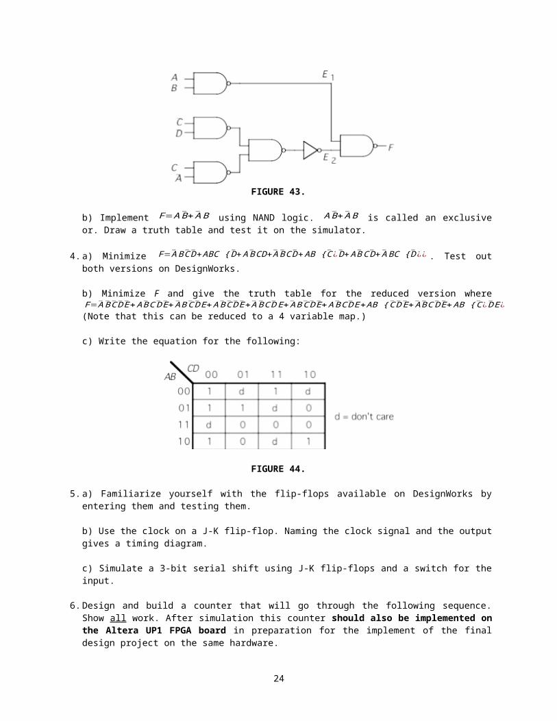
FIGURE 47. The completed circuit.
Warning: The current versions of LogicWorks may not default to gate delays of zero. If you are getting glitches and race conditions in your logic circuits it is acceptable to simply shorten or remove the gate delays from the simulations for this lab.
FPGA IMPLIMENTATION
The last requirement for the lab is to transfer the state machine design to the Altera UP1 FPGA board and demonstrate its functionality working on actual hardware. Partners for the Logic Experiment must be in the lab to complete this part with final check-off by the TA. Refer to the online manual FPGA tutorial for Logic project under Course Material on the course web page. There is also a zipped folder containing the files needed to demonstrate a counter circuit (bcounter.gdf) on the FPGA. There are several prepared prewired boards for use in the class stored in the cabinet in the back of the room on the podium’s right side. Do not remove the jumpers on the board. They are there to connect the switch inputs and LED/display outputs to the user’s logic circuit.
Unfortunately there is no automated way to transfer a logic circuit created in LogicWorks into the MAX+plus II 10.2 BASELINE software on the lab desktop PCs. Follow the steps in the tutorial to run the demo for the counter. After verifying the demo, create a new project and enter the logic circuit for the final project state machine. Once everything has been entered and working properly, demonstrate it to the TA for final check-off.
REFERENCES
[1] Huges, John L., Digital Computer Lab Workbook, Digital Equipment Corporation, 1969.
24

[2] Kohavi, Zvi, Switching and Finite Automata Theory, McGraw-Hill, 1970, Chapters 3, 4, 5, and 9.
[3] Mowle, F. W., A Systematic Approach to Digital Logic Design, Addison Wesley, 1976, Chapters 3, 4, 5, 8, and 9.
25