
MITIGATION OF SOFT ERRORS ON 65NM COMBINATIONAL LOGIC GATES VIA BUFFER GATE
13
International Journal of VLSI design & Communication Systems (VLSICS) Vol.6, No.3, June 2015 DOI : 10.5121/vlsic.2015.6301 1 MITIGATION OF SOFT ERRORS ON 65NM COMBINATIONAL LOGIC GATES VIA BUFFER GATE Ali Hosseini 1 and Hadi Jahanirad 2 1 Department of Electrical Engineering, Islamic Azad University, Science and Research branch, Kurdistan, Iran 2 Department of Electrical Engineering, Kurdistan University, Sanandaj, Iran ABSTRACT Through technology development, VLSI fabrication is becoming smaller in size which causes much sensitivity of VLSI circuit to noise effects especially soft error. In this paper, we present a method to mitigate soft error in combinational logic gates based on 65 nm technology that is able to reduce the possibility of noise propagation in combinational logic gate. We evaluate our result based on ISCAS 85 benchmark circuit. Through DFS algorithm and using analytical model derived by stimulation of each combinational logic gate in transistor layer, soft error is processed in paths of ISCAS 85 circuit benchmark and a single buffer logic gate is added to the end of the paths that have more potential to be affected by soft error. Therefore, possibility of soft error distribution through circuit benchmark is measured. The buffer gates that mitigate soft errors on the benchmark paths are kept and others are eliminated. After processing, new circuit benchmark is available that includes added buffer logic gate to only critical paths. This is more reliable than initial ISCAS85 circuit benchmark in terms of illuminating soft error. The results show that possibility of soft error distribution is reduced intelligently and due to adding buffer gate to just suspicious paths of benchmark, power and delay are optimum. KEYWORDS Logic gate, ISCAS85, soft error, Benchmark circuit& noise 1. INTRODUCTION Soft errors derived in the production of a voltage transient at a combinational circuit node. This is caused by the strike of an ionizing particle that deposits an amount of charge at the node parasitic capacitance [1]. Such perturbation can propagate within the combinational block and eventually reach a memory element that might erroneously change its stored value because of soft error.Soft error is extensively studied and propagation within given circuits are understood. Four factors contribute in deriving soft error [3]. 1) The voltage perturbation must have the appropriated electrical characteristics to traverse logic gates, 2) There must be a sensitized logic path for the perturbation to travel from oriented node to the memory element. 3) The voltage perturbation must be capable of switching the memory element state, and 4) the voltage perturbation must arrive within a time window during which the memory element is transparent. First, soft error
-
Upload
vlsics -
Category
Engineering
-
view
25 -
download
0
Transcript of MITIGATION OF SOFT ERRORS ON 65NM COMBINATIONAL LOGIC GATES VIA BUFFER GATE
International Journal of VLSI design & Communication Systems (VLSICS) Vol.6, No.3, June 2015
DOI : 10.5121/vlsic.2015.6301 1
MITIGATION OF SOFT ERRORS ON 65NM
COMBINATIONAL LOGIC GATES VIA BUFFER
GATE
Ali Hosseini1 and Hadi Jahanirad
2
1Department of Electrical Engineering, Islamic Azad University,
Science and Research branch, Kurdistan, Iran 2Department of Electrical Engineering, Kurdistan University, Sanandaj, Iran
ABSTRACT
Through technology development, VLSI fabrication is becoming smaller in size which causes much
sensitivity of VLSI circuit to noise effects especially soft error. In this paper, we present a method to
mitigate soft error in combinational logic gates based on 65 nm technology that is able to reduce the
possibility of noise propagation in combinational logic gate. We evaluate our result based on ISCAS 85
benchmark circuit. Through DFS algorithm and using analytical model derived by stimulation of each
combinational logic gate in transistor layer, soft error is processed in paths of ISCAS 85 circuit benchmark
and a single buffer logic gate is added to the end of the paths that have more potential to be affected by soft
error. Therefore, possibility of soft error distribution through circuit benchmark is measured. The buffer
gates that mitigate soft errors on the benchmark paths are kept and others are eliminated. After processing,
new circuit benchmark is available that includes added buffer logic gate to only critical paths. This is more
reliable than initial ISCAS85 circuit benchmark in terms of illuminating soft error. The results show that
possibility of soft error distribution is reduced intelligently and due to adding buffer gate to just suspicious
paths of benchmark, power and delay are optimum.
KEYWORDS
Logic gate, ISCAS85, soft error, Benchmark circuit& noise
1. INTRODUCTION
Soft errors derived in the production of a voltage transient at a combinational circuit node. This is
caused by the strike of an ionizing particle that deposits an amount of charge at the node parasitic
capacitance [1]. Such perturbation can propagate within the combinational block and eventually
reach a memory element that might erroneously change its stored value because of soft error.Soft
error is extensively studied and propagation within given circuits are understood. Four factors
contribute in deriving soft error [3]. 1) The voltage perturbation must have the appropriated
electrical characteristics to traverse logic gates, 2) There must be a sensitized logic path for the
perturbation to travel from oriented node to the memory element. 3) The voltage perturbation
must be capable of switching the memory element state, and 4) the voltage perturbation must
arrive within a time window during which the memory element is transparent. First, soft error
International Journal of VLSI design & Communication Systems (VLSICS) Vol.6, No.3, June 2015
2
propagation models were developed in [8], [9]. In [4] gate delay was described by modelling and
formulating voltage pulse propagation. In the past, soft error was just concerned in space
application. Nowadays, due to minimized size of fabrication technology, reduced power voltage
and tendency to maximize integration, there is a lot of potential for soft error distribution in
combinational logic circuits. In this work, by using the analytical model of soft error in previous
researches, we represent a method to reduce soft error scattered in Combinational logic circuits
which costs more delay and power consumption. This research is based on simulation test in 65
nm technology and uses ISCAS85 benchmark to evaluate test result. Since combinational logic
circuits also compose sequential logic circuits; so results can be extended in future as well.
2. GATE-LEVEL SOFT ERROR PROPAGATION MODEL
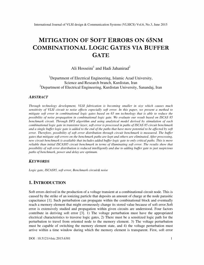
Two main parameters for measuring soft error distribution in logic gates are amplitude and pulse
width [2]. In this paper, we use circuit model showed in figure 1 for injecting soft errors to
combinational logic gates as well as extracting output result [8].Simulated soft errors are
produced at injector inverter output including amplitude and pulse width, which are injected to
logic gate respectively (HSPICE library gates) and soft error effect is measured on load inverter
output. Variety of simulated soft error pulses are produced by changing capacitor capacity and
input voltage [8]. In this work, soft errors are simulated in input of gate library and injected to
each combinational logic gate.
Figure1. Circuit model for extracting soft error parameters [8]
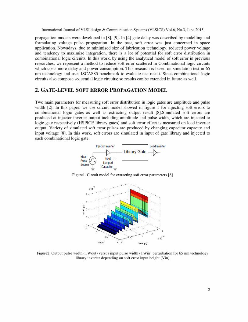
Figure2. Output pulse width (TWout) versus input pulse width (TWin) perturbation for 65 nm technology
library inverter depending on soft error input height (Vin)
International Journal of VLSI design & Communication Systems (VLSICS) Vol.6, No.3, June 2015
3
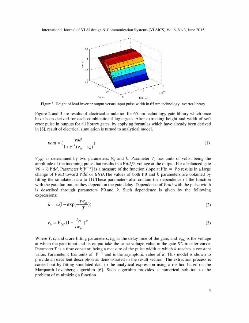
Figure3. Height of load inverter output versus input pulse width in 65 nm technology inverter library
Figure 2 and 3 are results of electrical simulation for 65 nm technology gate library which once
have been derived for each combinational logic gate. After extracting height and width of soft
error pulse in outputs for all library gates, by applying formulas which have already been derived
in [8], result of electrical simulation is turned to analytical model.
))(1
(0vve
vddvout
in
k−+
=−
(1)
���� is determined by two parameters: �� and �. Parameter �� has units of volts; being the
amplitude of the incoming pulse that results in a ���/2 voltage at the output. For a balanced gate
V0 ~ ½ ���. Parameter �[���] is a measure of the function slope at ��� = �� results in a large
change of ���� toward ��� or ���.The values of both �0 and � parameters are obtained by
fitting the simulated data to (1).These parameters also contain the dependence of the function
with the gate fan-out, as they depend on the gate delay. Dependence of ���� with the pulse width
is described through parameters �0.and �. Such dependence is given by the following
expressions:
))exp(1.(T
twck in
−−= (2)
α)1( 10
in
dDC
tw
tVv += (3)
Where �, �, and α are fitting parameters; ��� is the delay time of the gate; and ��� is the voltage
at which the gate input and its output take the same voltage value in the gate � transfer curve.
Parameter � is a time constant; being a measure of the pulse width at which � reaches a constant
value. Parameter � has units of ��� and is the asymptotic value of �. This model is shown to
provide an excellent description as demonstrated in the result section. The extraction process is
carried out by fitting simulated data to the analytical expression using a method based on the
Marquardt-Levenberg algorithm [6]. Such algorithm provides a numerical solution to the
problem of minimizing a function.

International Journal of VLSI design & Communication Systems (VLSICS) Vol.6, No.3, June 2015
4
bt
twttwatw
i
in
inout +−
+= )exp(.. 0 (4)
This expression provides an increasing curve for low �!"# values. Parameter $ was found to vary
linearly with �_�� following the expression.
invaaa .10 += (5)
And values of parameters in (5) were found to be approximately $�=1 and $�=0.4 for all library
gates in a 65 nm CMOS commercial technology. Parameter b in (4) is also described as a linear
function of �"#:
invbbb .10 += (6)
Where &� and &� are extracted for each gate. The parameters of the exponential term in (4) are
approximately the same for all library gates: ��=20 ps and �"=100 ps. The first one is a constant
of the attenuation of the exponential term. Figure 4 shows the width of soft error in the output of
inverter gate versus the height and width of soft error in the gate input.
Figure 4
Figure 5
International Journal of VLSI design & Communication Systems (VLSICS) Vol.6, No.3, June 2015
5
This analysis is done for all combinational logic gates. The comparison of formula model with
electrical simulation of soft error shows a good agreement for 65nm technology.
3. TEST AND MITIGATION IN ISCAS85 CIRCUIT BENCHMARK
3.1 TR CURVE
The varying height of gate output depends on both width and height of input. It means if input
height reaches to trigger threshold but the width is not yet in trigger region, soft error will not be
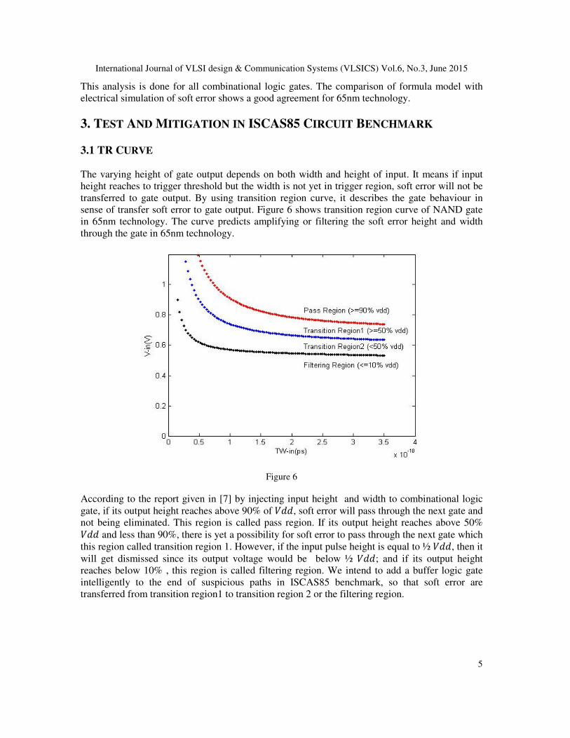
transferred to gate output. By using transition region curve, it describes the gate behaviour in
sense of transfer soft error to gate output. Figure 6 shows transition region curve of NAND gate
in 65nm technology. The curve predicts amplifying or filtering the soft error height and width
through the gate in 65nm technology.
Figure 6
According to the report given in [7] by injecting input height and width to combinational logic
gate, if its output height reaches above 90% of ���, soft error will pass through the next gate and
not being eliminated. This region is called pass region. If its output height reaches above 50%
��� and less than 90%, there is yet a possibility for soft error to pass through the next gate which
this region called transition region 1. However, if the input pulse height is equal to ½ ���, then it
will get dismissed since its output voltage would be below ½ ���; and if its output height
reaches below 10% , this region is called filtering region. We intend to add a buffer logic gate
intelligently to the end of suspicious paths in ISCAS85 benchmark, so that soft error are
transferred from transition region1 to transition region 2 or the filtering region.
International Journal of VLSI design & Communication Systems (VLSICS) Vol.6, No.3, June 2015
6
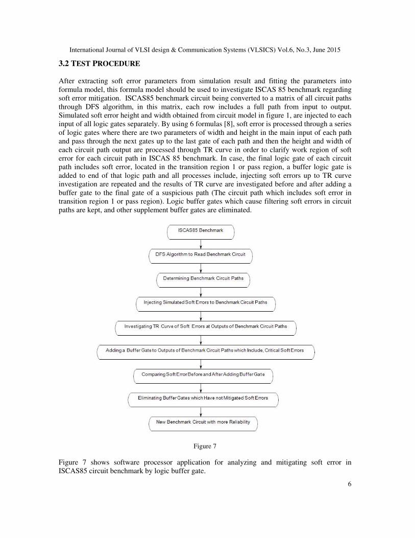
3.2 TEST PROCEDURE
After extracting soft error parameters from simulation result and fitting the parameters into
formula model, this formula model should be used to investigate ISCAS 85 benchmark regarding
soft error mitigation. ISCAS85 benchmark circuit being converted to a matrix of all circuit paths
through DFS algorithm, in this matrix, each row includes a full path from input to output.
Simulated soft error height and width obtained from circuit model in figure 1, are injected to each
input of all logic gates separately. By using 6 formulas [8], soft error is processed through a series
of logic gates where there are two parameters of width and height in the main input of each path
and pass through the next gates up to the last gate of each path and then the height and width of
each circuit path output are processed through TR curve in order to clarify work region of soft
error for each circuit path in ISCAS 85 benchmark. In case, the final logic gate of each circuit
path includes soft error, located in the transition region 1 or pass region, a buffer logic gate is
added to end of that logic path and all processes include, injecting soft errors up to TR curve
investigation are repeated and the results of TR curve are investigated before and after adding a
buffer gate to the final gate of a suspicious path (The circuit path which includes soft error in
transition region 1 or pass region). Logic buffer gates which cause filtering soft errors in circuit
paths are kept, and other supplement buffer gates are eliminated.
Figure 7
Figure 7 shows software processor application for analyzing and mitigating soft error in
ISCAS85 circuit benchmark by logic buffer gate.
International Journal of VLSI design & Communication Systems (VLSICS) Vol.6, No.3, June 2015
7
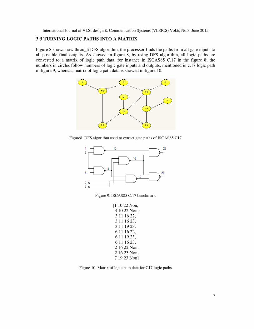
3.3 TURNING LOGIC PATHS INTO A MATRIX
Figure 8 shows how through DFS algorithm, the processor finds the paths from all gate inputs to
all possible final outputs. As showed in figure 8, by using DFS algorithm, all logic paths are
converted to a matrix of logic path data. for instance in ISCAS85 C.17 in the figure 8; the
numbers in circles follow numbers of logic gate inputs and outputs, mentioned in c.17 logic path
in figure 9, whereas, matrix of logic path data is showed in figure 10.
Figure8. DFS algorithm used to extract gate paths of ISCAS85 C17
Figure 9. ISCAS85 C.17 benchmark
[1 10 22 Non,
3 10 22 Non,
3 11 16 22,
3 11 16 23,
3 11 19 23,
6 11 16 22,
6 11 19 23,
6 11 16 23,
2 16 22 Non,
2 16 23 Non,
7 19 23 Non]
Figure 10. Matrix of logic path data for C17 logic paths
International Journal of VLSI design & Communication Systems (VLSICS) Vol.6, No.3, June 2015
8
[NAND NAND Non,
NAND NAND Non,
NAND NAND NAND,
NAND NAND NAND,
NAND NAND NAND,
NAND NAND NAND,
NAND NAND NAND,
NAND NAND NAND,
NAND NAND Non,
NAND NAND Non,
NAND NAND Non]
Figure 11. Matrix of logic gate data for C17 logic paths
Figure 11 shows corresponding logic gate for each node of logic path. Soft error height and width
are injected to each and every node separately. By reaching to each logic gate, processor reads its
gate name in matrix and applies corresponding model parameter to the soft error analysis
formulas and after soft error analysis in that gate, then goes to the next gates up to the end of
matrix row.
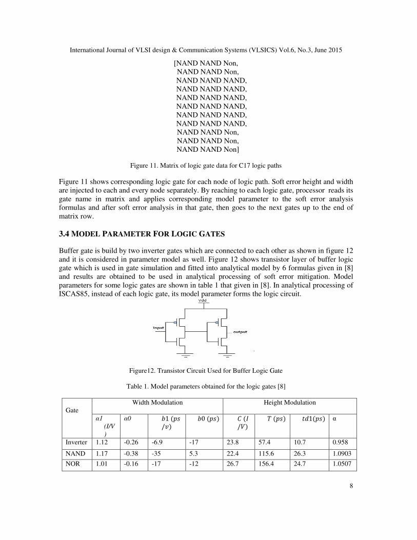
3.4 MODEL PARAMETER FOR LOGIC GATES
Buffer gate is build by two inverter gates which are connected to each other as shown in figure 12
and it is considered in parameter model as well. Figure 12 shows transistor layer of buffer logic
gate which is used in gate simulation and fitted into analytical model by 6 formulas given in [8]
and results are obtained to be used in analytical processing of soft error mitigation. Model
parameters for some logic gates are shown in table 1 that given in [8]. In analytical processing of
ISCAS85, instead of each logic gate, its model parameter forms the logic circuit.
Figure12. Transistor Circuit Used for Buffer Logic Gate
Table 1. Model parameters obtained for the logic gates [8]
Gate
Width Modulation Height Modulation
α1
(I/V
)
α0 &1 ()*
/�)
&0 ()*) (,
/�)
� ()*) ��1()*) α
Inverter 1.12 -0.26 -6.9 -17 23.8 57.4 10.7 0.958
NAND 1.17 -0.38 -35 5.3 22.4 115.6 26.3 1.0903
NOR 1.01 -0.16 -17 -12 26.7 156.4 24.7 1.0507
International Journal of VLSI design & Communication Systems (VLSICS) Vol.6, No.3, June 2015
9
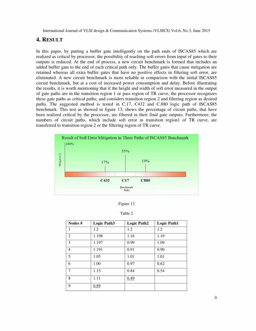
4. RESULT
In this paper, by putting a buffer gate intelligently on the path ends of ISCAS85 which are
realized as critical by processor, the possibility of reaching soft errors from input of gates to their
outputs is reduced. At the end of process, a new circuit benchmark is formed that includes an
added buffer gate to the end of each critical path only. The buffer gates that cause mitigation are
retained whereas all extra buffer gates that have no positive effects in filtering soft error, are
eliminated. A new circuit benchmark is more reliable in comparison with the initial ISCAS85
circuit benchmark, but at a cost of increased power consumption and delay. Before illustrating
the results, it is worth mentioning that if the height and width of soft error measured in the output
of gate paths are in the transition region 1 or pass region of TR curve, the processor recognizes
these gate paths as critical paths; and considers transition region 2 and filtering region as desired
paths. The suggested method is tested in C.17, C432 and C.880 logic path of ISCAS85
benchmark. This test as showed in figure 13, shows the percentage of circuit paths, that have
been realized critical by the processor, are filtered in their final gate outputs. Furthermore, the
numbers of circuit paths, which include soft error in transition region1 of TR curve, are
transferred to transition region 2 or the filtering region of TR curve.
Figure 13
Table 2
Nodes # Logic Path3 Logic Path2 Logic Path1
1 1.2 1.2 1.2
2 1.198 1.16 1.19
3 1.197 0.99 1.09
4 1.191 0.91 0.90
5 1.05 1.01 1.01
6 1.00 0.97 0.62
7 1.15 0.84 0.54
8 1.11 0.49
9 0.89
International Journal of VLSI design & Communication Systems (VLSICS) Vol.6, No.3, June 2015
10
Table 2 shows a logic path taken from a C880 ISCAS85 benchmark circuit. For instance, the
simulated soft error [7] with 0.2 V height and 60 ps width is injected to the first input of logic
path1 and at the end of the path height of 0.54V is measured. Because this amount of height is
located in transition region 2 of TR curve, the processor does not consider it as a critical region
and keeps the logic path without any modification. At the last output of logic path 2, the amount
of 0.84V is measured for the same input parameters. Because this amount of height is located in
the transition region1 of TR curve, the processor considers it as critical and adds a logic buffer
gate to the end of logic path 2. Then, injecting soft error after adding buffer is repeated and the
height of logic path 2 reduced from 0.84V to 0.49 V because logic path 2 is transferred from the
transition region1 to transition region 2. It means mitigation is done and the processor records the
buffer logic gate at the end of path 2 for the new modified circuit benchmark. At the last output
of logic path 3, 1.11V is measured, which is realized as critical by the processor and a buffer
logic gate is added to the end of logic path 3. In spite of adding this gate, the height and width of
path 3 outputs are still located in the transition region 1 of TR curve. Even though soft error
mitigation for logic path 3 failed, the processor eliminates the added buffer gate from path output
and does not record the buffer gate in path 3 for the new circuit benchmark. The figures that are
underlined in table 2 are output height of the added buffer gate. Table 3 shows few instances for
soft error mitigation, that are done on C.17,C880 and C432 logic paths, include combinational
logic gates in ISCAS85 benchmark.
Table 3. Result of soft error mitigation in ISCAS85 benchmark logic paths
ISCAS85 benchmark logic paths C.17 C.880 C.432
Total logic paths 11 419 585
logic paths including critical soft errors 11 178 54
Eliminated critical soft errors at logic path outputs 6 33 10
Remained critical soft errors at logic path outputs 5 145 44
For instance, in ISCAS85 C.432 benchmark path, the processor determines all gate paths from
input to output through DFS algorithm, (All gate paths include each and every gate input in
ISCAS85 C.432 benchmark and its gate paths to all possible final gate outputs) that are 585
paths. Then, by passing simulated soft error through the whole gate paths, 54 paths are detected
in transition region1 of TR curve and the processor identifies it as a critical region and adds a
logic gate buffer to all final outputs of these 54 logic paths. Again, simulated soft errors are
passed from the 54 paths to determine the effect of buffer added to the end of paths. Results show
that 10 paths out of 54 paths are transferred from the transition region1 to the transition region 2
and these 10 paths are not located in the critical region of TR curve. Then, the processor
eliminates 44 added buffer gates which have not been mitigating any soft errors in order to
prevent extra power and delay in ISCAS85 C.432.
In ISCAS85 C17 benchmark, all 11 logic paths are recognized by DFS algorithm and because
they are realized as critical region of TR curve, all logic paths reach to added buffer gate at the
end of their own path outputs. After adding buffer gate soft errors at outputs, 6 paths out of 11
paths are transferred from the transition region 1 to the transition region 2 and are not located in
the critical region. Other 5 logic paths that are not collaborating in soft error mitigation but due to
being in common path output with the 6 paths mitigating soft error, no buffer gate is eliminated.
Consequently a new ISCAS85 C.17 benchmark is formed by 2 added buffer logic gates.

International Journal of VLSI design & Communication Systems (VLSICS) Vol.6, No.3, June 2015
11
Figure14. New form of ISCAS85 C17 benchmark after adding logic buffer gates
Table 4[7]
nodes# Logic path
height of Inv
chain 3
Logic path
height of Inv
chain 2
Logic path
height of
Inv chain 1
INV001 0.73 0.83 0.79
INV002 0.76 0.84 0.85
INV003 0.75 0.88 0.84
INV004 0.76 0.87 0.85
INV0017 0.78 0.98 0.74
INV0018 0.77 0.97 0.75
INV0019 0.78 0.99 0.73
INV020 0.77 0.98 0.74
INV067 0.78 1.33 0.37
INV068 0.77 1.32 0.38
INV069 0.78 1.34 0.35
INV0128 0.77 1.74 0
INV0129 0.78 1.76 0
INV0249 0.78 2.59 0
INV250 0.77 2.58 0
In a previous work, soft error mitigation by chain of inverters is considered. According to the
results shown in [7], in some cases after passing soft error from the inverter gate, the height
increases so it can cause even transferring from the transition region 2 to the critical region of TR
curve. The recommended idea in this paper, putting buffer gates intelligently through processing
application prevents this error. Because buffer gate just in a case its ability to reduce effect of soft
errors, is added to the output. Table 4 shows the derived height of the consecutive chain of
inverter gate; as shown in this table, in some cases the inverter gate causes a reduction in height
and in other cases it causes an increase in height. Therefore, the recommended idea in this paper
has some benefits in comparing: First, buffer gate is not added to all path outputs, though the new
circuit benchmark fabrication costs less. Second, it prevents burden of extra power and delay to
circuit benchmark. In addition, comprehensive automatic analyzer of ISACS85 soft error, is
represented, which can be applied for new researches in the future.
5. CONCLUSION
Nowadays, along with the deteriorating size of fabrication in VLSI circuits and the reduction in
power voltage in logic gates, the sensitivity of circuits are enhanced. Therefore, in this paper by
utilization analytical processing for 65nm technology library, critical path by reference to TR
curve is recognized and by adding a buffer logic gate to the end of logic path, the effect of soft

International Journal of VLSI design & Communication Systems (VLSICS) Vol.6, No.3, June 2015
12
error is declined and due to adding buffer gate to the critical path only, power and delay are
optimized. The recommended method is capable of processing mass of logic paths in ISCAS85
circuit benchmark in sense of soft error by utilization of DFS algorithm. As a result of applying
our idea on standard circuit benchmark ISCAS85, reliable results are expected. The simple
structure of buffer gate which includes only 2 PMOS gates and 2 NMOS gates placed only at the
end of gate paths, making the modification easier and cheaper. By applying simulated soft errors
that are done in a previous research to transistor layer of combinational logic gates in 65nm
library technology, the height and width of input and output are obtained to be fitted into
analytical model, and then the derived results are used in analytical processing of soft error
mitigation.
The final result shows that for all combinational logic paths in ISCAS85 minimum 17% and
maximum 55% of soft errors in critical region (transition region 1) are transferred to the
mitigation region (filtering or transition region 2) and then new circuit benchmark including
added logic buffer gate has more reliability in sense of soft error than ISCAS85 circuit
benchmark. Also we found that by adding buffer logic gate to end of logic path, it is not possible
to filter soft error that is located in pass region of TR curve.
REFERENCES [1] B. Narasimham, B. L. Bhuva, R. D. Schrimpf, L. W. Massengill, M.J. Gadlage, O. A. Amusan, W. T.
Holman, A. F. Witulski, W. H. Robinson, J. D. Black, J. M. Benedetto, and P. H. Eaton,
“Characterization of digital single event transient pulse widths in 130 nm CMOS,” IEEE Trans. Nucl.
Sci., vol. 54, pp. 2506–2511, 2007.
[2] F. Moll and A. Rubio, “Spurious signals in digital CMOS VLSI circuits: A propagation analysis,”
IEEE Trans. Circuits Syst. II, vol. 39, no. 10, pp. 749–752, Oct. 1992.
[3] V. Zolotov, D. Blaauw, S. Sirichotiyakul, M. Becer, C. Oh, R. Panda, A. Grinshpon, and R. Levy,
“Noise propagation and failure criteria for VLSI designs,” in Proc. IEEE Int. Conf. Computer Aided
Design (ICCAD), 2002, pp. 587–594
[4] G. I. Wirth, M. G. Vieira, and F. G. L. Kastensmidt, “Accurate and computer efficient modeling of
single event transients in CMOS circuits,” IET Circuits Devices Syst., vol. 1, no. 2, pp. 137–142,
2007.
[5] J. Velamala, R. LiVolsi, M. Torres, and Y. Cao, “Design sensitivity of single event transients in
scaled logic circuits,” in Proc. Design Automation Conf. (DAC), 2011, pp. 694–699.
[6] P. C. Gregory, Bayesian Logical Data Analysis for the Physical Sciences: A Comparative Approach
With Mathematica Support. Cambridge, U.K.: Cambridge Univ. Press, 2005.
[7] G.Wirth, F. L. Kastensmidt, and I. Ribeiro, “Single event transients in logic circuits-load and
propagation induced pulse broadening,” IEEE Trans. Nucl. Sci., vol. 55, no. 6, pp. 2928–2935, 2008.
[8] Gili, X., Barcelo, S., Bota, S.A., and Segura, J., “Analytical Modeling of Single Event Transients
Propagation in Combinational Logic Gates” Trans. Nucl. Sci., vol. 59, no. 4, pp. 971–979, 2012.
[9] S. Rezgui, J. McCollum, and R. Won, “Design and layout effects on SET propagation in 90-nm ASIC
and FPGA test structures,” IEEE Trans. Nucl. Sci., vol. 57, no. 6, pp. 3716–3724, 2010.
[10] L. Entrena, A. Lindoso, M. G. Valderas,M. Portela, and C. L. Ongil, “Analysis of SET effects in a
PIC microprocessor for selective hardening,” IEEE Trans. Nucl. Sci., vol. 58, no. 3, pp. 1078–1085,
2011.
[11] D. Kobayashi, K. Hirose, V. Ferlet-Cavrois, D. McMorrow, T. Makino, H. Ikeda, Y. Arai, and M.
Ohno, “Device-physics-based analytical model for single-event transients in SOI CMOS logic,”
IEEE Trans. Nucl. Sci., vol. 56, no. 6, pp. 3043–3049, 2009.
[12] F. Moll and A. Rubio, “Spurious signals in digital CMOS VLSI circuits: A propagation analysis,”
IEEE Trans. Circuits Syst. II, vol. 39, no. 10, pp. 749–752, Oct. 1992.
International Journal of VLSI design & Communication Systems (VLSICS) Vol.6, No.3, June 2015
13
[13] D. Rossi, J. Cazeaux, M. Omaña, C. Metra, and A. Chatterjee, “Accurate linear model for SET
critical charge estimation,” IEEE Trans. Very Large Scale Integr. (VLSI) Syst., vol. 17, no. 8, pp.
1161–1166, 2009.
[14] M. J. Gadlage, J. R. Ahlbin, B. L. Bhuva, N. C. Hooten, N. A. Dodds, R. A. Reed, L. W. Massengill,
R. D. Schrimpf, and G. Vizkelethy, “Alpha-particle and focused-ion-beam-induced single-event
transient measurements in a bulk 65-nm CMOS technology,” IEEE Trans. Nucl.Sci., vol. 58, pp.
1093–1097, Jun. 2011.
AUTHORS
Ali Hosseini received his B.Sc. in electronics engineering from applied science and
technology university, Arak, Iran in 2011 and his M.Sc. degree in electronics
engineering from Science and Research branch of IAU in 2014, Kurdistan, Iran. And His
research interests include VLSI circuits Design, Embedded system, Fault Tolerant
computing and Biomedical Electronics.
Hadi Jahanirad received his B.Sc. in electronics engineering from K.N.T.U, Tehran, Iran
in 2008 and M.Sc. and PhD in electronics engineering from Iran university of Science and technology,
Tehran, Iran respectively in 2008 and 2013. He is currently assistant professor in faculty of electrical
engineering of Kurdistan University. His research interests include VLSI circuits design and analysis
system, Analog integrated circuits design and analysis, RF Microelectronics, Embedded systems, Fault
tolerant systems and Reconfigurable computing.