Combinational Logic Design Principles. Combinational...
37
Combinational Logic Design Principles. Combinational Circuits Analysis and Synthesis Doru Todinca Department of Computers Politehnica University of Timisoara
-
Upload
hoangduong -
Category
Documents
-
view
235 -
download
0
Transcript of Combinational Logic Design Principles. Combinational...
Combinational Logic Design Principles.
Combinational Circuits Analysis and Synthesis
Doru Todinca
Department of Computers
Politehnica University of Timisoara
Outline
Combinational Circuits Analysis
Combinational-Circuit SynthesisCircuit Descriptions and DesignsCircuit ManipulationsCombinational-Circuit Minimization
Outline
Combinational Circuits Analysis
Combinational-Circuit SynthesisCircuit Descriptions and DesignsCircuit ManipulationsCombinational-Circuit Minimization
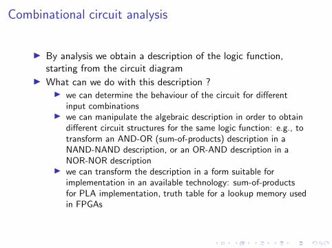
Combinational circuit analysis
◮ By analysis we obtain a description of the logic function,starting from the circuit diagram
◮ What can we do with this description ?◮ we can determine the behaviour of the circuit for different
input combinations◮ we can manipulate the algebraic description in order to obtain
different circuit structures for the same logic function: e.g., totransform an AND-OR (sum-of-products) description in aNAND-NAND description, or an OR-AND description in aNOR-NOR description
◮ we can transform the description in a form suitable forimplementation in an available technology: sum-of-productsfor PLA implementation, truth table for a lookup memory usedin FPGAs
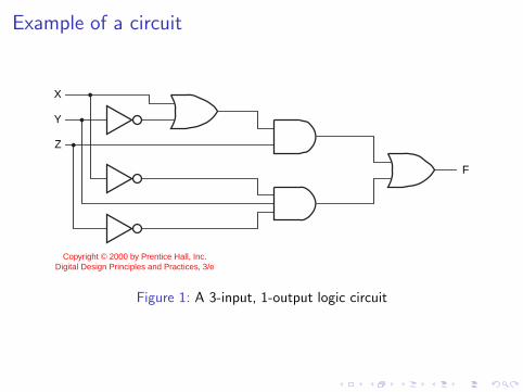
Example of a circuit
F
X
Y
Z
Copyright © 2000 by Prentice Hall, Inc. Digital Design Principles and Practices, 3/e
Figure 1: A 3-input, 1-output logic circuit
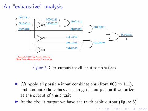
An “exhaustive” analysis
01100101
01000101
00100000
11001111
01010101
11110000
01010101
00110011 11001100
00110011
10101010
0000111100001111
F
X
Y
Z
Copyright © 2000 by Prentice Hall, Inc. Digital Design Principles and Practices, 3/e
Figure 2: Gate outputs for all input combinations
◮ We apply all possible input combinations (from 000 to 111),and compute the values at each gate’s output until we arriveat the output of the circuit
◮ At the circuit output we have the truth table output (figure 3)
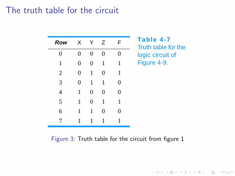
The truth table for the circuit
Row X Y Z F Table 4-7Truth table for the logic circuit of Figure 4-9.
0 0 0 0 0
1 0 0 1 1
2 0 1 0 1
3 0 1 1 0
4 1 0 0 0
5 1 0 1 1
6 1 1 0 0
7 1 1 1 1
Figure 3: Truth table for the circuit from figure 1
F
X
YY′
X + Y′
(X + Y′ ) • Z
X′
Z′
Z
= ((X + Y′ ) • Z) + (X′ • Y • Z′)
X′ • Y • Z′
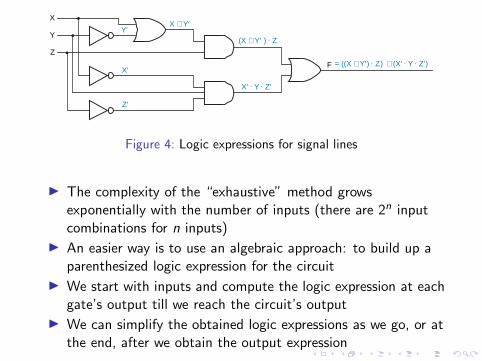
Figure 4: Logic expressions for signal lines
◮ The complexity of the “exhaustive” method growsexponentially with the number of inputs (there are 2n inputcombinations for n inputs)
◮ An easier way is to use an algebraic approach: to build up aparenthesized logic expression for the circuit
◮ We start with inputs and compute the logic expression at eachgate’s output till we reach the circuit’s output
◮ We can simplify the obtained logic expressions as we go, or atthe end, after we obtain the output expression
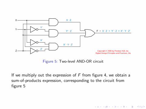
F = X • Z + Y′ • Z + X′ • Y • Z′
X
Y
Z
Y′ Y′ • Z
X • Z
X′ • Y • Z′
X′
Z′ Copyright © 2000 by Prentice Hall, Inc.
Digital Design Principles and Practices, 3/e
Figure 5: Two-level AND-OR circuit
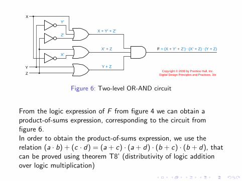
If we multiply out the expression of F from figure 4, we obtain asum-of-products expression, corresponding to the circuit fromfigure 5
X
Y
Z
Y′
Y + Z
X′ + Z
X + Y′ + Z′
X′
Z′
F = (X + Y′ + Z′) • (X′ + Z) • (Y + Z)
Copyright © 2000 by Prentice Hall, Inc. Digital Design Principles and Practices, 3/e
Figure 6: Two-level OR-AND circuit
From the logic expression of F from figure 4 we can obtain aproduct-of-sums expression, corresponding to the circuit fromfigure 6.In order to obtain the product-of-sums expression, we use therelation (a · b) + (c · d) = (a + c) · (a + d) · (b + c) · (b + d), thatcan be proved using theorem T8’ (distributivity of logic additionover logic multiplication)
An example with NAND and NOR gates
F
X
W
Y
Z
= [((W • X′)′ • Y)′ + (W′ + X + Y′)′ + (W + Z)′]′
X′ (W • X′)′
((W • X′)′ • Y)′
(W′ + X + Y′)′
(W + Z)′
W′
Y′
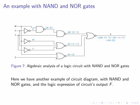
Figure 7: Algebraic analysis of a logic circuit with NAND and NOR gates
Here we have another example of circuit diagram, with NAND andNOR gates, and the logic expression of circuit’s output F .
Applying graphically DeMorgan’s theorems
F
X
W
Y
Z
= ((W′ + X) • Y) • (W′ + X + Y′)• (W + Z)
X′ W′ + X
((W′ + X) • Y)′
(W′ + X + Y′)′
(W + Z)′
W′
Y′
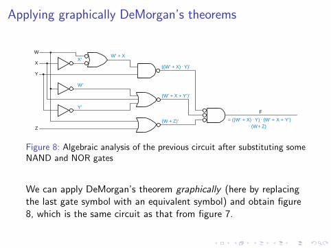
Figure 8: Algebraic analysis of the previous circuit after substituting someNAND and NOR gates
We can apply DeMorgan’s theorem graphically (here by replacingthe last gate symbol with an equivalent symbol) and obtain figure8, which is the same circuit as that from figure 7.
A different circuit for the same logic function
F
X
W
Y
Z
= ((W′ + X) • Y) • (W′ + X + Y′)• (W + Z)
X′ W′ + X
(W′ + X) • Y
W′ + X + Y′
W + Z
W′
Y′
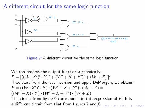
Figure 9: A different circuit for the same logic function
We can process the output function algebraically:F = [((W · X ′)′ · Y )′ + (W ′ + X + Y ′)′ + (W + Z )′]′
If we start from the last inversion and apply DeMorgan, we obtain:F = ((W · X ′)′ · Y ) · (W ′ + X + Y ′) · (W + Z ) =((W ′ + X ) · Y ) · (W ′ + X + Y ′) · (W + Z )The circuit from figure 9 corresponds to this expression of F . It isa different circuit from that from figures 7 and 8.
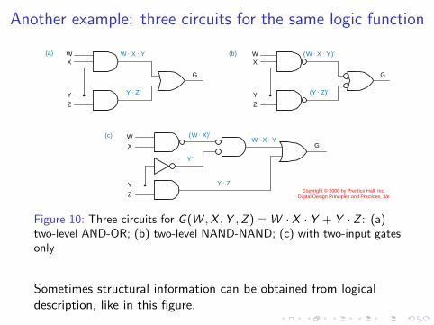
Another example: three circuits for the same logic function
WX
Y
Z
G
(a) (b)
(c)
WX
Y
Z
G
GW
X
Y
Z
Y′
W • X • Y
W • X • Y
(W • X • Y)′
(W • X)′
(Y • Z)′ Y • Z
Y • ZCopyright © 2000 by Prentice Hall, Inc.
Digital Design Principles and Practices, 3/e
Figure 10: Three circuits for G(W ,X ,Y ,Z ) = W · X · Y + Y · Z : (a)two-level AND-OR; (b) two-level NAND-NAND; (c) with two-input gatesonly
Sometimes structural information can be obtained from logicaldescription, like in this figure.
Outline
Combinational Circuits Analysis
Combinational-Circuit SynthesisCircuit Descriptions and DesignsCircuit ManipulationsCombinational-Circuit Minimization
Combinational-Circuit Synthesis: Introduction
◮ Usually the starting point for the combinational circuit designis a word description (given or developed by ourselves)
◮ We can translate this word description in a HDL (see thehigh-level description of the multiplexer in VHDL)
◮ Then the HDL tools can realize an automatic synthesis of thecircuit
◮ However, it is important for us to be able to synthesize(combinational) circuits by hand for the following reasons:◮ sometimes the circuit obtained by automatic synthesis simply
isn’t good enough: e.g., for critical parts of a design, likecertain parts from a microprocessor
◮ sometimes the automatic tool “runs amok” and obtain a verypoor result
◮ Hence, it is important to be able at least to evaluate the resultof the synthesis process and, if the performance of theobtained circuit is not good enough, to improve it
Outline
Combinational Circuits Analysis
Combinational-Circuit SynthesisCircuit Descriptions and DesignsCircuit ManipulationsCombinational-Circuit Minimization
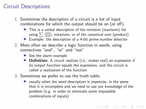
Circuit Descriptions
1. Sometimes the description of a circuit is a list of inputcombinations for which the output should be on (or off).◮ This is a verbal description of the minterm (maxterm) list
using∑
(∏), notations, or of the canonical sum (product)
◮ Example: the description of a 4-bit prime-number detector
2. More often we describe a logic function in words, usingconnectives “and”, “or” and “not”◮ See the alarm example◮ Definition: A circuit realizes (i.e., makes real) an expression if
its output function equals the expression, and the circuit iscalled a realization of the function.
3. Sometimes we prefer to use the truth table:◮ usually when the word description is imprecise, in the sense
that it is incomplete and we need to use our knowledge of theproblem (e.g. in order to eliminate some impossiblecombinations of inputs)
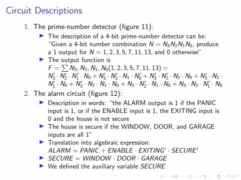
Circuit Descriptions
1. The prime-number detector (figure 11):◮ The description of a 4-bit prime-number detector can be:
“Given a 4-bit number combination N = N3N2N1N0, producea 1 output for N = 1, 2, 3, 5, 7, 11, 13, and 0 otherwise”
◮ The output function isF =
∑N3,N2,N1,N0(1, 2, 3, 5, 7, 11, 13) =
N ′
3 ·N′
2 ·N′
1 ·N0 +N ′
3 ·N′
2 ·N1 ·N′
0 +N ′
3 ·N′
2 ·N1 ·N0 +N ′
3 ·N2 ·
N ′
1 ·N0 +N ′
3 · N2 ·N1 · N0 +N3 ·N′
2 · N1 ·N0 +N3 · N2 ·N′
1 · N0
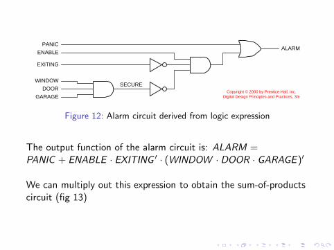
2. The alarm circuit (figure 12):◮ Description in words: “the ALARM output is 1 if the PANIC
input is 1, or if the ENABLE input is 1, the EXITING input is0 and the house is not secure
◮ The house is secure if the WINDOW, DOOR, and GARAGEinputs are all 1”
◮ Translation into algebraic expression:ALARM = PANIC + ENABLE · EXITING ′
· SECURE ′
◮ SECURE = WINDOW · DOOR · GARAGE◮ We defined the auxiliary variable SECURE
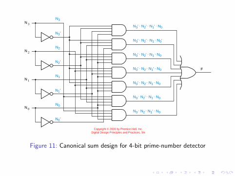
N 3
N3
N3′
N3′ • N2′ • N1′ • N0
N3′ • N2′ • N1 • N0′
N3′ • N2′ • N1 • N0
N3′ • N2 • N1′ • N0
N3′ • N2 • N1 • N0
N3 • N2′ • N1 • N0
N3 • N2 • N1′ • N0
N2
N2′
N1
N1′
N0
N0′
N 2
N 1
N 0
F
Copyright © 2000 by Prentice Hall, Inc. Digital Design Principles and Practices, 3/e
Figure 11: Canonical sum design for 4-bit prime-number detector
PANICALARM
ENABLE
EXITING
WINDOW
DOOR
GARAGE
SECURECopyright © 2000 by Prentice Hall, Inc.
Digital Design Principles and Practices, 3/e
Figure 12: Alarm circuit derived from logic expression
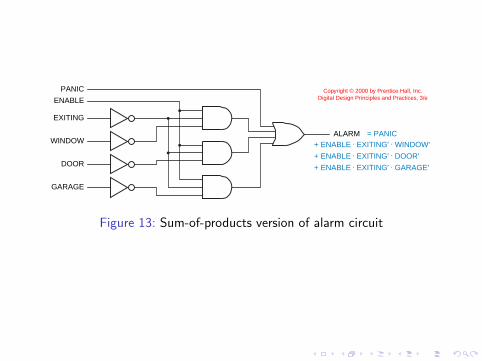
The output function of the alarm circuit is: ALARM =PANIC + ENABLE · EXITING ′
· (WINDOW · DOOR · GARAGE )′
We can multiply out this expression to obtain the sum-of-productscircuit (fig 13)
PANIC
ALARM
ENABLE
EXITING
WINDOW
DOOR
GARAGE
= PANIC+ ENABLE • EXITING′ • WINDOW′ + ENABLE • EXITING′ • DOOR′ + ENABLE • EXITING′ • GARAGE′
Copyright © 2000 by Prentice Hall, Inc. Digital Design Principles and Practices, 3/e
Figure 13: Sum-of-products version of alarm circuit
Outline
Combinational Circuits Analysis
Combinational-Circuit SynthesisCircuit Descriptions and DesignsCircuit ManipulationsCombinational-Circuit Minimization
Circuit Manipulation
◮ Remember that NAND and NOR gates are faster (andcheaper) that AND and OR gates in many technologies (e.g.CMOS, TTL)
◮ However, usually we describe a problem in a “natural” wayusing propositions with AND and OR, not with NAND andNOR
◮ It means that sometimes we obtain a circuit diagram withAND and OR gates, and want to transform it with NAND andNOR gates
◮ Figure 14 gives such an example of transformation, startingfrom a sum-of-products form
◮ In figure 14 the inverters needed to complement the inputs arenot shown.
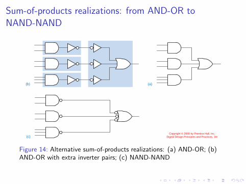
Sum-of-products realizations: from AND-OR to
NAND-NAND
(c)
(a)(b)
Copyright © 2000 by Prentice Hall, Inc. Digital Design Principles and Practices, 3/e
Figure 14: Alternative sum-of-products realizations: (a) AND-OR; (b)AND-OR with extra inverter pairs; (c) NAND-NAND
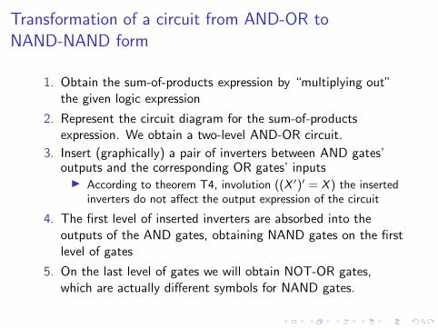
Transformation of a circuit from AND-OR to
NAND-NAND form
1. Obtain the sum-of-products expression by “multiplying out”the given logic expression
2. Represent the circuit diagram for the sum-of-productsexpression. We obtain a two-level AND-OR circuit.
3. Insert (graphically) a pair of inverters between AND gates’outputs and the corresponding OR gates’ inputs◮ According to theorem T4, involution ((X ′)′ = X ) the inserted
inverters do not affect the output expression of the circuit
4. The first level of inserted inverters are absorbed into theoutputs of the AND gates, obtaining NAND gates on the firstlevel of gates
5. On the last level of gates we will obtain NOT-OR gates,which are actually different symbols for NAND gates.
Transformation of a circuit from AND-OR to
NAND-NAND form
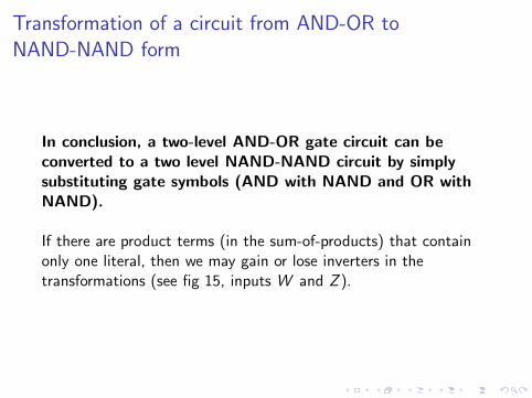
In conclusion, a two-level AND-OR gate circuit can beconverted to a two level NAND-NAND circuit by simplysubstituting gate symbols (AND with NAND and OR withNAND).
If there are product terms (in the sum-of-products) that containonly one literal, then we may gain or lose inverters in thetransformations (see fig 15, inputs W and Z ).
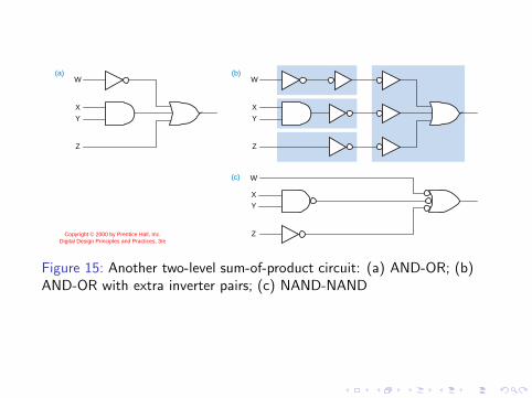
(a)W
X
Y
Z
(c) W
X
Y
Z
(b)W
X
Y
Z
Copyright © 2000 by Prentice Hall, Inc. Digital Design Principles and Practices, 3/e
Figure 15: Another two-level sum-of-product circuit: (a) AND-OR; (b)AND-OR with extra inverter pairs; (c) NAND-NAND
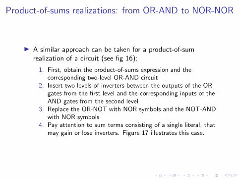
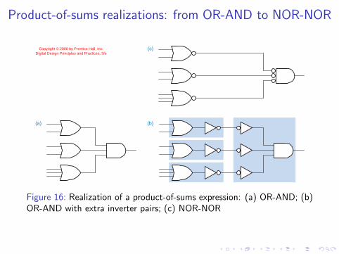
Product-of-sums realizations: from OR-AND to NOR-NOR
◮ A similar approach can be taken for a product-of-sumrealization of a circuit (see fig 16):
1. First, obtain the product-of-sums expression and thecorresponding two-level OR-AND circuit
2. Insert two levels of inverters between the outputs of the ORgates from the first level and the corresponding inputs of theAND gates from the second level
3. Replace the OR-NOT with NOR symbols and the NOT-ANDwith NOR symbols
4. Pay attention to sum terms consisting of a single literal, thatmay gain or lose inverters. Figure 17 illustrates this case.
Product-of-sums realizations: from OR-AND to NOR-NOR
(a) (b)
(c)Copyright © 2000 by Prentice Hall, Inc. Digital Design Principles and Practices, 3/e
Figure 16: Realization of a product-of-sums expression: (a) OR-AND; (b)OR-AND with extra inverter pairs; (c) NOR-NOR
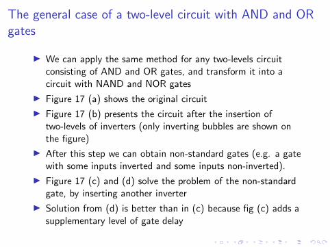
The general case of a two-level circuit with AND and OR
gates
◮ We can apply the same method for any two-levels circuitconsisting of AND and OR gates, and transform it into acircuit with NAND and NOR gates
◮ Figure 17 (a) shows the original circuit
◮ Figure 17 (b) presents the circuit after the insertion oftwo-levels of inverters (only inverting bubbles are shown onthe figure)
◮ After this step we can obtain non-standard gates (e.g. a gatewith some inputs inverted and some inputs non-inverted).
◮ Figure 17 (c) and (d) solve the problem of the non-standardgate, by inserting another inverter
◮ Solution from (d) is better than in (c) because fig (c) adds asupplementary level of gate delay
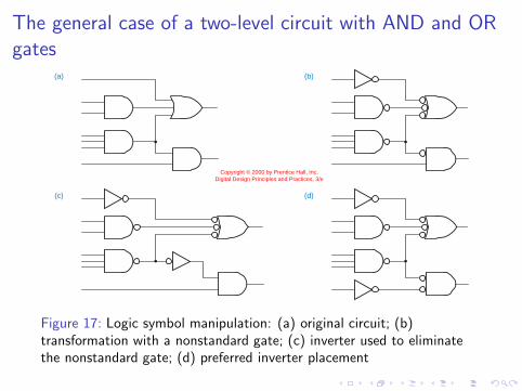
The general case of a two-level circuit with AND and OR
gates(a) (b)
(d)(c)
Copyright © 2000 by Prentice Hall, Inc. Digital Design Principles and Practices, 3/e
Figure 17: Logic symbol manipulation: (a) original circuit; (b)transformation with a nonstandard gate; (c) inverter used to eliminatethe nonstandard gate; (d) preferred inverter placement
Outline
Combinational Circuits Analysis
Combinational-Circuit SynthesisCircuit Descriptions and DesignsCircuit ManipulationsCombinational-Circuit Minimization
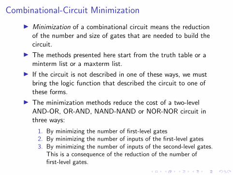
Combinational-Circuit Minimization
◮ Minimization of a combinational circuit means the reductionof the number and size of gates that are needed to build thecircuit.
◮ The methods presented here start from the truth table or aminterm list or a maxterm list.
◮ If the circuit is not described in one of these ways, we mustbring the logic function that described the circuit to one ofthese forms.
◮ The minimization methods reduce the cost of a two-levelAND-OR, OR-AND, NAND-NAND or NOR-NOR circuit inthree ways:
1. By minimizing the number of first-level gates2. By minimizing the number of inputs of the first-level gates3. By minimizing the number of inputs of the second-level gates.
This is a consequence of the reduction of the number offirst-level gates.
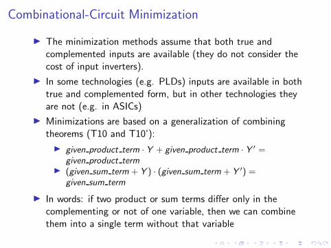
Combinational-Circuit Minimization
◮ The minimization methods assume that both true andcomplemented inputs are available (they do not consider thecost of input inverters).
◮ In some technologies (e.g. PLDs) inputs are available in bothtrue and complemented form, but in other technologies theyare not (e.g. in ASICs)
◮ Minimizations are based on a generalization of combiningtheorems (T10 and T10’):
◮ given product term · Y + given product term · Y ′ =given product term
◮ (given sum term + Y ) · (given sum term + Y ′) =given sum term
◮ In words: if two product or sum terms differ only in thecomplementing or not of one variable, then we can combinethem into a single term without that variable
Combinational-Circuit Minimization
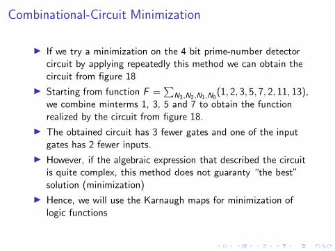
◮ If we try a minimization on the 4 bit prime-number detectorcircuit by applying repeatedly this method we can obtain thecircuit from figure 18
◮ Starting from function F =∑
N3,N2,N1,N0(1, 2, 3, 5, 7, 2, 11, 13),
we combine minterms 1, 3, 5 and 7 to obtain the functionrealized by the circuit from figure 18.
◮ The obtained circuit has 3 fewer gates and one of the inputgates has 2 fewer inputs.
◮ However, if the algebraic expression that described the circuitis quite complex, this method does not guaranty “the best”solution (minimization)
◮ Hence, we will use the Karnaugh maps for minimization oflogic functions
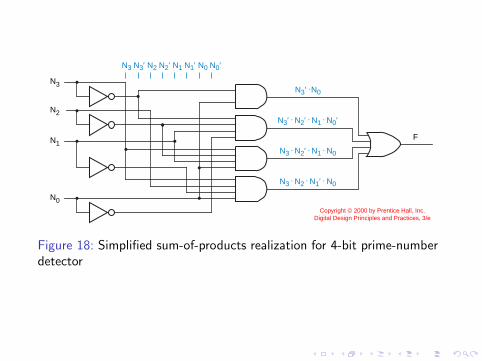
N3
N2
N1
N0
F
N3 N3′ N2 N2′ N1 N1′ N0 N0′
N3′ • N0
N3′ • N2′ • N1 • N0′
N3 • N2′ • N1 • N0
N3 • N2 • N1′ • N0
Copyright © 2000 by Prentice Hall, Inc. Digital Design Principles and Practices, 3/e
Figure 18: Simplified sum-of-products realization for 4-bit prime-numberdetector