bq2412x Single-Chip Switched-Mode, Li-Ion, and Li … · 3 in 4 in 6 vcc 2 stat1 19 stat2 5 pg 7...
40
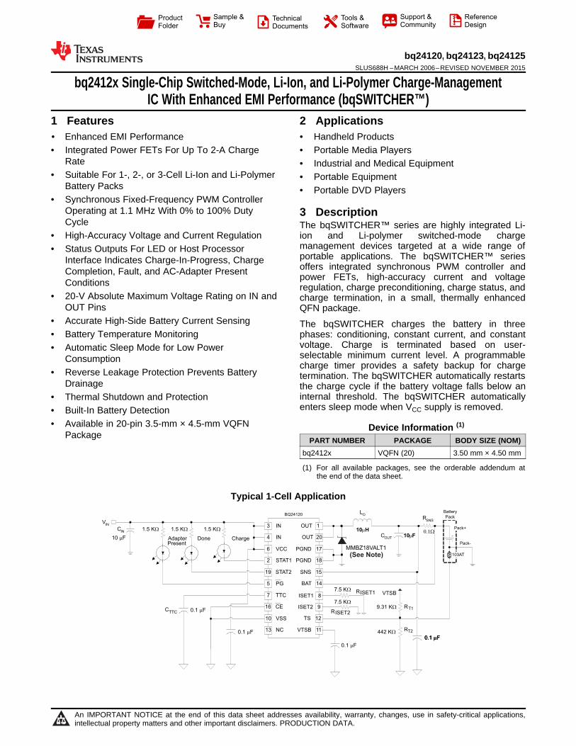
3 IN 4 IN 6 VCC 2 STAT1 19 STAT2 5 PG 7 TTC 16 CE 10 VSS 13 NC OUT 1 OUT 20 PGND 17 PGND 18 SNS 15 BAT 14 ISET1 8 ISET2 9 TS 12 VTSB 11 V IN 10mF 10mH L O C IN C OUT R SNS 0.1W 1.5 KW 1.5 KW 1.5 KW Charge Done Adapter Present 7.5 KW 7.5 KW 0.1 F m 9.31 KW 442 KW VTSB R T1 R T2 R R ISET1 ISET2 103AT Battery Pack Pack- Pack+ 0.1 F m 0.1 F m 0.1 F m 10 F m C TTC BQ24120 0.1 F m 0.1 F m MMBZ18VALT1 (See Note) Product Folder Sample & Buy Technical Documents Tools & Software Support & Community Reference Design bq24120, bq24123, bq24125 SLUS688H – MARCH 2006 – REVISED NOVEMBER 2015 bq2412x Single-Chip Switched-Mode, Li-Ion, and Li-Polymer Charge-Management IC With Enhanced EMI Performance (bqSWITCHER™) 1 Features 2 Applications 1• Enhanced EMI Performance • Handheld Products • Integrated Power FETs For Up To 2-A Charge • Portable Media Players Rate • Industrial and Medical Equipment • Suitable For 1-, 2-, or 3-Cell Li-Ion and Li-Polymer • Portable Equipment Battery Packs • Portable DVD Players • Synchronous Fixed-Frequency PWM Controller Operating at 1.1 MHz With 0% to 100% Duty 3 Description Cycle The bqSWITCHER™ series are highly integrated Li- • High-Accuracy Voltage and Current Regulation ion and Li-polymer switched-mode charge management devices targeted at a wide range of • Status Outputs For LED or Host Processor portable applications. The bqSWITCHER™ series Interface Indicates Charge-In-Progress, Charge offers integrated synchronous PWM controller and Completion, Fault, and AC-Adapter Present power FETs, high-accuracy current and voltage Conditions regulation, charge preconditioning, charge status, and • 20-V Absolute Maximum Voltage Rating on IN and charge termination, in a small, thermally enhanced OUT Pins QFN package. • Accurate High-Side Battery Current Sensing The bqSWITCHER charges the battery in three • Battery Temperature Monitoring phases: conditioning, constant current, and constant voltage. Charge is terminated based on user- • Automatic Sleep Mode for Low Power selectable minimum current level. A programmable Consumption charge timer provides a safety backup for charge • Reverse Leakage Protection Prevents Battery termination. The bqSWITCHER automatically restarts Drainage the charge cycle if the battery voltage falls below an internal threshold. The bqSWITCHER automatically • Thermal Shutdown and Protection enters sleep mode when V CC supply is removed. • Built-In Battery Detection • Available in 20-pin 3.5-mm × 4.5-mm VQFN Device Information (1) Package PART NUMBER PACKAGE BODY SIZE (NOM) bq2412x VQFN (20) 3.50 mm × 4.50 mm (1) For all available packages, see the orderable addendum at the end of the data sheet. Typical 1-Cell Application 1 An IMPORTANT NOTICE at the end of this data sheet addresses availability, warranty, changes, use in safety-critical applications, intellectual property matters and other important disclaimers. PRODUCTION DATA.
Transcript of bq2412x Single-Chip Switched-Mode, Li-Ion, and Li … · 3 in 4 in 6 vcc 2 stat1 19 stat2 5 pg 7...
3 IN
4 IN
6 VCC
2 STAT1
19 STAT2
5 PG
7 TTC
16 CE
10 VSS
13 NC
OUT 1
OUT 20
PGND 17
PGND 18
SNS 15
BAT 14
ISET1 8
ISET2 9
TS 12
VTSB 11
VIN
10mF10mH
LO
CIN
COUT
RSNS
0.1W1.5 KW 1.5 KW 1.5 KW
ChargeDoneAdapterPresent
7.5 KW
7.5 KW
0.1 Fm
9.31 KW
442 KW
VTSB
RT1
RT2
R
R
ISET1
ISET2
103AT
Battery
Pack
Pack-
Pack+
0.1 Fm0.1 Fm
0.1 Fm
10 Fm
CTTC
BQ24120
0.1 Fm0.1 Fm
MMBZ18VALT1
(See Note)
Product
Folder
Sample &Buy
Technical
Documents
Tools &
Software
Support &Community
ReferenceDesign
bq24120, bq24123, bq24125SLUS688H –MARCH 2006–REVISED NOVEMBER 2015
bq2412x Single-Chip Switched-Mode, Li-Ion, and Li-Polymer Charge-ManagementIC With Enhanced EMI Performance (bqSWITCHER™)
1 Features 2 Applications1• Enhanced EMI Performance • Handheld Products• Integrated Power FETs For Up To 2-A Charge • Portable Media Players
Rate • Industrial and Medical Equipment• Suitable For 1-, 2-, or 3-Cell Li-Ion and Li-Polymer • Portable Equipment
Battery Packs • Portable DVD Players• Synchronous Fixed-Frequency PWM Controller
Operating at 1.1 MHz With 0% to 100% Duty 3 DescriptionCycle The bqSWITCHER™ series are highly integrated Li-
• High-Accuracy Voltage and Current Regulation ion and Li-polymer switched-mode chargemanagement devices targeted at a wide range of• Status Outputs For LED or Host Processorportable applications. The bqSWITCHER™ seriesInterface Indicates Charge-In-Progress, Chargeoffers integrated synchronous PWM controller andCompletion, Fault, and AC-Adapter Present power FETs, high-accuracy current and voltageConditions regulation, charge preconditioning, charge status, and
• 20-V Absolute Maximum Voltage Rating on IN and charge termination, in a small, thermally enhancedOUT Pins QFN package.
• Accurate High-Side Battery Current Sensing The bqSWITCHER charges the battery in three• Battery Temperature Monitoring phases: conditioning, constant current, and constant
voltage. Charge is terminated based on user-• Automatic Sleep Mode for Low Powerselectable minimum current level. A programmableConsumptioncharge timer provides a safety backup for charge
• Reverse Leakage Protection Prevents Battery termination. The bqSWITCHER automatically restartsDrainage the charge cycle if the battery voltage falls below an
internal threshold. The bqSWITCHER automatically• Thermal Shutdown and Protectionenters sleep mode when VCC supply is removed.• Built-In Battery Detection
• Available in 20-pin 3.5-mm × 4.5-mm VQFN Device Information (1)Package PART NUMBER PACKAGE BODY SIZE (NOM)
bq2412x VQFN (20) 3.50 mm × 4.50 mm
(1) For all available packages, see the orderable addendum atthe end of the data sheet.
Typical 1-Cell Application
1
An IMPORTANT NOTICE at the end of this data sheet addresses availability, warranty, changes, use in safety-critical applications,intellectual property matters and other important disclaimers. PRODUCTION DATA.
bq24120, bq24123, bq24125SLUS688H –MARCH 2006–REVISED NOVEMBER 2015 www.ti.com
Table of Contents8.4 Device Functional Modes........................................ 211 Features .................................................................. 1
9 Application and Implementation ........................ 222 Applications ........................................................... 19.1 Application Information............................................ 223 Description ............................................................. 19.2 Typical Application .................................................. 224 Revision History..................................................... 29.3 System Examples ................................................... 265 Device Options....................................................... 3
10 Power Supply Recommendations ..................... 296 Pin Configuration and Functions ......................... 311 Layout................................................................... 297 Specifications......................................................... 4
11.1 Layout Guidelines ................................................. 297.1 Absolute Maximum Ratings ..................................... 411.2 Layout Example .................................................... 307.2 ESD Ratings ............................................................ 411.3 Thermal Considerations ........................................ 307.3 Recommended Operating Conditions....................... 5
12 Device and Documentation Support ................. 317.4 Thermal Information ................................................. 512.1 Documentation Support ........................................ 317.5 Electrical Characteristics........................................... 512.2 Related Links ........................................................ 317.6 Dissipation Ratings ................................................... 812.3 Community Resources.......................................... 317.7 Typical Characteristics .............................................. 912.4 Trademarks ........................................................... 318 Detailed Description ............................................ 1112.5 Electrostatic Discharge Caution............................ 318.1 Overview ................................................................. 1112.6 Glossary ................................................................ 318.2 Functional Block Diagram ....................................... 12
13 Mechanical, Packaging, and Orderable8.3 Feature Description................................................. 13Information ........................................................... 31
4 Revision History
Changes from Revision G (August 2008) to Revision H Page
• Added ESD Ratings table, Feature Description section, Device Functional Modes, Application and Implementationsection, Power Supply Recommendations section, Layout section, Device and Documentation Support section, andMechanical, Packaging, and Orderable Information section .................................................................................................. 1
2 Submit Documentation Feedback Copyright © 2006–2015, Texas Instruments Incorporated
Product Folder Links: bq24120 bq24123 bq24125
STAT1
IN
IN
PG
VCC
TTC
ISET1
ISET2
STAT2
PGND
PGND
CE
SNS
BAT
CELLS
TS
OU
T
OU
TV
TS
B
VS
S
201
1110
2
3
4
5
6
7
8
9
19
18
17
16
15
14
13
12
bq24120, bq24123, bq24125www.ti.com SLUS688H –MARCH 2006–REVISED NOVEMBER 2015
5 Device Options
CHARGE REGULATION INTENDEDPART NUMBER (1) (2)VOLTAGE (V) APPLICATION
BQ24120RHLR / BQ24120RHLT 4.2 VStand-alone
4.2 V / 8.4 VBQ24123RHLR / BQ24123RHLT
2.1 V to 15.5 V Externally programmable
(1) The RHL package is available in the following options:R - taped and reeled in quantities of 3,000 devices per reelT - taped and reeled in quantities of 250 devices per reel
(2) This product is RoHS compatible, including a lead concentration that does not exceed 0.1% of total product weight, and is suitable foruse in specified lead-free soldering processes.
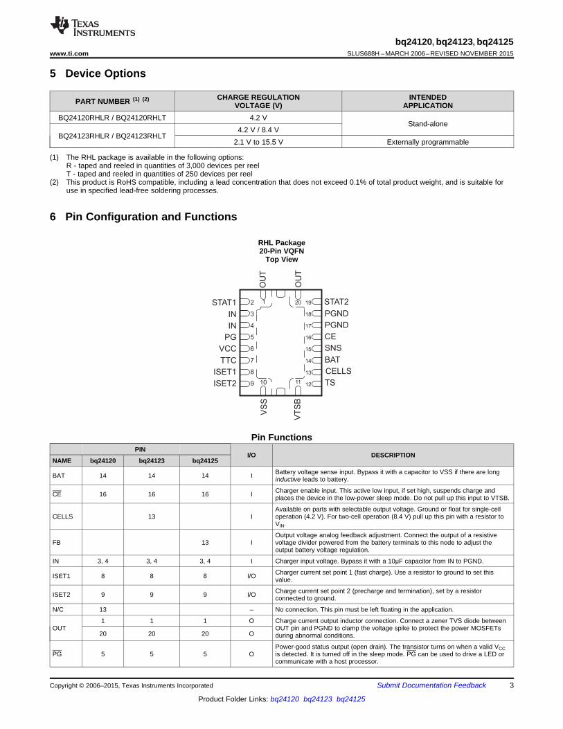
6 Pin Configuration and Functions
RHL Package20-Pin VQFN
Top View
Pin FunctionsPIN
I/O DESCRIPTIONNAME bq24120 bq24123 bq24125
Battery voltage sense input. Bypass it with a capacitor to VSS if there are longBAT 14 14 14 I inductive leads to battery.
Charger enable input. This active low input, if set high, suspends charge andCE 16 16 16 I places the device in the low-power sleep mode. Do not pull up this input to VTSB.
Available on parts with selectable output voltage. Ground or float for single-cellCELLS 13 I operation (4.2 V). For two-cell operation (8.4 V) pull up this pin with a resistor to
VIN.
Output voltage analog feedback adjustment. Connect the output of a resistiveFB 13 I voltage divider powered from the battery terminals to this node to adjust the
output battery voltage regulation.
IN 3, 4 3, 4 3, 4 I Charger input voltage. Bypass it with a 10μF capacitor from IN to PGND.
Charger current set point 1 (fast charge). Use a resistor to ground to set thisISET1 8 8 8 I/O value.
Charge current set point 2 (precharge and termination), set by a resistorISET2 9 9 9 I/O connected to ground.
N/C 13 – No connection. This pin must be left floating in the application.
1 1 1 O Charge current output inductor connection. Connect a zener TVS diode betweenOUT OUT pin and PGND to clamp the voltage spike to protect the power MOSFETs
20 20 20 O during abnormal conditions.
Power-good status output (open drain). The transistor turns on when a valid VCCPG 5 5 5 O is detected. It is turned off in the sleep mode. PG can be used to drive a LED or
communicate with a host processor.
Copyright © 2006–2015, Texas Instruments Incorporated Submit Documentation Feedback 3
Product Folder Links: bq24120 bq24123 bq24125

bq24120, bq24123, bq24125SLUS688H –MARCH 2006–REVISED NOVEMBER 2015 www.ti.com
Pin Functions (continued)PIN
I/O DESCRIPTIONNAME bq24120 bq24123 bq24125
PGND 17,18 17,18 17,18 Power ground input
Charge current-sense input. Battery current is sensed via the voltage dropSNS 15 15 15 I developed on this pin by an external sense resistor in series with the battery pack.
A 0.1μF capacitor to VSS is required.
Charge status 1 (open-drain output). When the transistor turns on indicatesSTAT1 2 2 2 O charge in process. When it is off and with the condition of STAT2 indicates
various charger conditions (See Table 1)
Charge status 2 (open-drain output). When the transistor turns on indicatesSTAT2 19 19 19 O charge is done. When it is off and with the condition of STAT1 indicates various
charger conditions (See Table 1)
Temperature sense input. This input monitors its voltage against an internalTS 12 12 12 I threshold to determine if charging is allowed. Use an NTC thermistor and a
voltage divider powered from VTSB to develop this voltage. (See Figure 9)
Timer and termination control. Connect a capacitor from this node to VSS to setTTC 7 7 7 I the bqSWITCHER timer. When this input is low, the timer and termination
detection are disabled.
VCC 6 6 6 I Analog device input. A 0.1μF capacitor to VSS is required.
VSS 10 10 10 Analog ground input
TS internal bias regulator voltage. Connect capacitor (with a value between aVTSB 11 11 11 O 0.1μF and 1μF) between this output and VSS.
There is an internal electrical connection between the exposed thermal pad andExposed VSS. The exposed thermal pad must be connected to the same potential as theThermal Pad Pad Pad VSS pin on the printed circuit board. The power pad can be used as a star groundPad connection between VSS and PGND. A common ground plane may be used. VSS
pin must be connected to ground at all times.
7 Specifications
7.1 Absolute Maximum Ratings (1)
over operating free-air temperature range (unless otherwise noted)MIN MAX UNIT
Supply voltage (with respect to VSS) IN, VCC 20 VSTAT1, STAT2, PG, CE, CELLS, SNS, BAT –0.3 20 VOUT –0.7 20 V
Input voltage (with respect to VSS and PGND) TS, TTC 7 VVTSB 3.6 VISET1, ISET2 3.3 V
Voltage difference between SNS and BAT inputs (VSNS - VBAT) ±1 VOutput sink STAT1, STAT2, PG 10 mAOutput current (average) OUT 2.2 ALead temperature 1.6 mm (1/16 inch) from case for 10 seconds 300 °C
TA Operating free-air temperature –40 85 °CTJ Junction temperature –40 125 °CTstg Storage temperature –65 150 °C
(1) Stresses beyond those listed under Absolute Maximum Ratings may cause permanent damage to the device. These are stress ratingsonly, which do not imply functional operation of the device at these or any other conditions beyond those indicated under RecommendedOperating Conditions. Exposure to absolute-maximum-rated conditions for extended periods may affect device reliability.
7.2 ESD RatingsVALUE UNIT
Human-body model (HBM), per ANSI/ESDA/JEDEC JS-001 (1) ±2000V(ESD) Electrostatic discharge V
Charged-device model (CDM), per JEDEC specification JESD22-C101 (2) ±500
(1) JEDEC document JEP155 states that 500-V HBM allows safe manufacturing with a standard ESD control process.(2) JEDEC document JEP157 states that 250-V CDM allows safe manufacturing with a standard ESD control process.
4 Submit Documentation Feedback Copyright © 2006–2015, Texas Instruments Incorporated
Product Folder Links: bq24120 bq24123 bq24125

VIREG 1V
RSET1 1000,
bq24120, bq24123, bq24125www.ti.com SLUS688H –MARCH 2006–REVISED NOVEMBER 2015
7.3 Recommended Operating ConditionsMIN NOM MAX UNIT
Supply voltage, VCC and IN (Tie together) 4.35 (1) 16.0 (2) VOperating junction temperature range, TJ –40 125 °C
(1) The IC continues to operate below Vmin, to 3.5 V, but these conditions are not tested, and are not specified.(2) The inherent switching noise voltage spikes should not exceed the absolute maximum rating on either the IN or OUT pins. A tight layout
minimizes switching noise.
7.4 Thermal Informationbq2412x
THERMAL METRIC (1) RHL (VQFN) UNIT20 PINS
RθJA Junction-to-ambient thermal resistance 39.2 °C/WRθJC(top) Junction-to-case (top) thermal resistance 39.3 °C/WRθJB Junction-to-board thermal resistance 15.8 °C/WψJT Junction-to-top characterization parameter 0.6 °C/WψJB Junction-to-board characterization parameter 15.8 °C/WRθJC(bot) Junction-to-case (bottom) thermal resistance 3.6 °C/W
(1) For more information about traditional and new thermal metrics, see the Semiconductor and IC Package Thermal Metrics applicationreport, SPRA953.
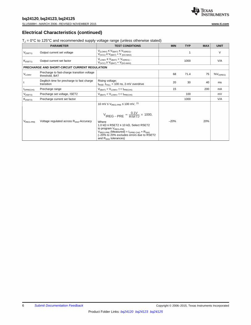
7.5 Electrical CharacteristicsTJ = 0°C to 125°C and recommended supply voltage range (unless otherwise stated)
PARAMETER TEST CONDITIONS MIN TYP MAX UNIT
INPUT CURRENTS
VCC > VCC(min), PWM switching 10mA
IVCC(VCC) VCC supply current VCC > VCC(min), PWM NOT switching 5
VCC > VCC(min), CE = HIGH 315 μA
0°C ≤ TJ ≤ 65°C, VI(BAT) = 4.2 V, 3.5VCC < V(SLP) or VCC > V(SLP) but not in charge
Battery discharge sleep current, (SNS, 0°C ≤ TJ ≤ 65°C, VI(BAT) = 8.4 V,I(SLP) 5.5 μABAT, OUT pins) VCC < V(SLP) or VCC > V(SLP) but not in charge
0°C ≤ TJ ≤ 65°C, VI(BAT) = 12.6 V, 7.7VCC < V(SLP) or VCC > V(SLP) but not in charge
VOLTAGE REGULATION
CELLS = Low, in voltage regulation 4.2Output voltage, bq24123
VOREG CELLS = High, in voltage regulation 8.4VOutput voltage, bq24120 Operating in voltage regulation 4.2
Feedback regulation REF for bq24125 onlyVIBAT IIBAT = 25 nA typical into pin 2.1(W/FB)
TA = 25°C –0.5% 0.5%Voltage regulation accuracy
–1% 1%
CURRENT REGULATION - FAST CHARGE
VLOWV ≤ VI(BAT) < VOREG,IOCHARGE Output current range of converter 150 2000 mAV(VCC) - VI(BAT) > V(DO-MAX)
100 mV ≤ VIREG≤ 200 mV, (1)
VIREG Voltage regulated across R(SNS) Accuracy –10% 10%Programmed Where5 kΩ ≤ RSET1 ≤ 10 kΩ, Select RSET1 toprogram VIREG,VIREG(measured) = IOCHARGE ×RSNS(–10% to 10% excludes errors due to RSET1and R(SNS) tolerances)
(1) Inductor peak current should be less than 2.6 A. Use equations 12, 13, 15, 18, and 19 to make sure the peak inductor current is lessthan 2.6 A.
Copyright © 2006–2015, Texas Instruments Incorporated Submit Documentation Feedback 5
Product Folder Links: bq24120 bq24123 bq24125
VIREGPRE0.1V
RSET2 1000,
bq24120, bq24123, bq24125SLUS688H –MARCH 2006–REVISED NOVEMBER 2015 www.ti.com
Electrical Characteristics (continued)TJ = 0°C to 125°C and recommended supply voltage range (unless otherwise stated)
PARAMETER TEST CONDITIONS MIN TYP MAX UNIT
V(LOWV) ≤ VI(BAT) ≤ VO(REG),V(ISET1) Output current set voltage 1 VV(VCC) ≥ VI(BAT) + V (DO-MAX)
VLOWV ≤ VI(BAT) < VO(REG) ,K(ISET1) Output current set factor 1000 V/AV(VCC) ≥ VI(BAT) + V(DO-MAX)
PRECHARGE AND SHORT-CIRCUIT CURRENT REGULATION
Precharge to fast-charge transition voltageVLOWV 68 71.4 75 %VO(REG)threshold, BAT
Deglitch time for precharge to fast charge Rising voltage;t 20 30 40 mstransition tRISE, tFALL = 100 ns, 2-mV overdrive
IOPRECHG Precharge range VI(BAT) < VLOWV, t < tPRECHG 15 200 mA
V(ISET2) Precharge set voltage, ISET2 VI(BAT) < VLOWV, t < tPRECHG 100 mV
K(ISET2) Precharge current set factor 1000 V/A
10 mV ≤ VIREG-PRE ≤ 100 mV, (1)
VIREG-PRE Voltage regulated across RSNS-Accuracy –20% 20%Where1.0 kΩ ≤ RSET2 ≤ 10 kΩ, Select RSET2to program VIREG-PRE,VIREG-PRE (Measured) = IOPRE-CHG × RSNS(–20% to 20% excludes errors due to RSET2and RSNS tolerances)
6 Submit Documentation Feedback Copyright © 2006–2015, Texas Instruments Incorporated
Product Folder Links: bq24120 bq24123 bq24125

bq24120, bq24123, bq24125www.ti.com SLUS688H –MARCH 2006–REVISED NOVEMBER 2015
Electrical Characteristics (continued)TJ = 0°C to 125°C and recommended supply voltage range (unless otherwise stated)
PARAMETER TEST CONDITIONS MIN TYP MAX UNIT
CHARGE TERMINATION (CURRENT TAPER) DETECTION
ITERM Charge current termination detection range VI(BAT) > VOREG- VRCH 15 200 mA
Charge termination detection set voltage,VTERM VI(BAT) > VOREG- VRCH 100 mVISET2
K(ISET2) Termination current set factor 1000 V/A
Charger termination accuracy VI(BAT) > VOREG- VRCH –20% 20%
Both rising and falling,tdg-TERM Deglitch time for charge termination 20 30 40 ms2-mV overdrive tRISE, tFALL = 100 ns
TEMPERATURE COMPARATOR AND VTSB BIAS REGULATOR
%LTF Cold temperature threshold, TS, % of bias VLTF = VO(VTSB) × % LTF/100 72.8% 73.5% 74.2%
%HTF Hot temperature threshold, TS, % of bias VHTF = VO(VTSB) × % HTF/100 33.7% 34.4% 35.1%
Cutoff temperature threshold, TS, % of%TCO VTCO = VO(VTSB) × % TCO/100 28.7% 29.3% 29.9%bias
LTF hysteresis 0.5% 1.0% 1.5%
Both rising and falling,tdg-TS Deglitch time for temperature fault, TS 20 30 40 ms2-mV overdrive tRISE, tFALL = 100 ns
VCC > VIN(min),VO(VTSB) TS bias output voltage 3.15 VI(VTSB) = 10 mA 0.1 μF ≤ CO(VTSB) ≤ 1 μF
VCC > IN(min),VO(VTSB) TS bias voltage regulation accuracy –10% 10%I(VTSB) = 10 mA 0.1 μF ≤ CO(VTSB) ≤ 1 μF
BATTERY RECHARGE THRESHOLD
VRCH Recharge threshold voltage Below VOREG 75 100 125 mV/cell
VI(BAT) < decreasing below threshold,tdg-RCH Deglitch time 20 30 40 mstFALL = 100 ns 10-mV overdrive
STAT1, STAT2, AND PG OUTPUTS
VOL(STATx) Low-level output saturation voltage, STATx IO = 5 mA 0.5V
VOL(PG) Low-level output saturation voltage, PG IO = 10 mA 0.1
CE , CELLS INPUTS
VIL Low-level input voltage IIL = 5 μA 0 0.4V
VIH High-level input voltage IIH = 20 μA 1.3 VCC
TTC INPUT
tPRECHG Precharge timer 1440 1800 2160 s
tCHARGE Programmable charge timer range t(CHG) = C(TTC) × K(TTC) 25 572 minutes
Charge timer accuracy 0.01 μF ≤ C(TTC) ≤ 0.18 μF -10% 10%
KTTC Timer multiplier 2.6 min/nF
CTTC Charge time capacitor range 0.01 0.22 μF
VTTC_EN TTC enable threshold voltage V(TTC) rising 200 mV
SLEEP COMPARATOR
VCC ≤ VIBAT VCC ≤ VIBAT2.3 V ≤ VI(OUT) ≤ VOREG, for 1 or 2 cells +5 mV +75 mVVSLP-ENT Sleep-mode entry threshold V
VI(OUT) = 12.6 V, RIN = 1kΩ, VCC ≤ VIBAT VCC ≤ VIBATbq24125 (2) –4 mV +73 mV
VSLP-EXIT Sleep-mode exit hysteresis, 2.3 V ≤ VI(OUT)≤ VOREG 40 160 mV
VCC decreasing below threshold,tFALL = 100 ns, 10-mV overdrive, 5 μsPMOS turns off
tdg-SLP Deglitch time for sleep modeVCC decreasing below threshold,tFALL = 100 ns, 10-mV overdrive, 20 30 40 msSTATx pins turn off
UVLO
VUVLO-ON IC active threshold voltage VCC rising 3.15 3.30 3.50 V
IC active hysteresis VCC falling 120 150 mV
(2) For bq24125 only. RIN is connected between IN and PGND pins and needed to ensure sleep entry.
Copyright © 2006–2015, Texas Instruments Incorporated Submit Documentation Feedback 7
Product Folder Links: bq24120 bq24123 bq24125
bq24120, bq24123, bq24125SLUS688H –MARCH 2006–REVISED NOVEMBER 2015 www.ti.com
Electrical Characteristics (continued)TJ = 0°C to 125°C and recommended supply voltage range (unless otherwise stated)
PARAMETER TEST CONDITIONS MIN TYP MAX UNIT
PWM
7 V ≤ VCC ≤ VCC(max) 400Internal P-channel MOSFET on-resistance
4.5 V ≤ VCC ≤ 7 V 500mΩ
7 V ≤ VCC ≤ VCC(max) 130Internal N-channel MOSFET on-resistance
4.5 V ≤ VCC ≤ 7 V 150
fOSC Oscillator frequency 1.1 MHz
Frequency accuracy –9% 9%
DMAX Maximum duty cycle 100%
DMIN Minimum duty cycle 0%
tTOD Switching delay time (dead time) 20 ns
tsyncmin Minimum synchronous FET on time 60 ns
Synchronous FET minimum current-off 50 400 mAthreshold (3)
BATTERY DETECTION
Battery detection current during time-outIDETECT VI(BAT) < VOREG – VRCH 2 mAfault
IDISCHRG1 Discharge current VSHORT < VI(BAT) < VOREG – VRCH 400 μA
tDISCHRG1 Discharge time VSHORT < VI(BAT) < VOREG – VRCH 1 s
IWAKE Wake current VSHORT < VI(BAT) < VOREG – VRCH 2 mA
tWAKE Wake time VSHORT < VI(BAT) < VOREG – VRCH 0.5 s
Begins after termination detected,IDISCHRG2 Termination discharge current 400 μAVI(BAT) ≤ VOREG
tDISCHRG2 Termination time 262 ms
OUTPUT CAPACITOR
Required output ceramic capacitor rangeCOUT from SNS to PGND, between inductor and 4.7 10 47 μF
RSNS
Required SNS capacitor (ceramic) at SNSCSNS 0.1 μFpin
PROTECTION
Threshold over VOREG to turn off P-channelVOVP OVP threshold voltage MOSFET, STAT1, and STAT2 during charge 110 117 121 %VO(REG)
or termination states
ILIMIT Cycle-by-cycle current limit 2.6 3.6 4.5 A
VSHORT Short-circuit voltage threshold, BAT VI(BAT) falling 1.95 2 2.05 V/cell
ISHORT Short-circuit current VI(BAT) ≤ VSHORT 35 65 mA
TSHTDWN Thermal trip 165°C
Thermal hysteresis 10
(3) N-channel always turns on for approximately 60 ns and then turns off if current is too low.
7.6 Dissipation RatingsTA < 40°C DERATING FACTORPACKAGE ΘJA ΘJC POWER RATING ABOVE TA = 40°C
RHL (1) 46.87°C/W 2.15°C/W 1.81 W 0.021 W/°C
(1) This data is based on using the JEDEC High-K board, and the exposed die pad is connected to a copper pad on the board. This isconnected to the ground plane by a 2x3 via matrix.
8 Submit Documentation Feedback Copyright © 2006–2015, Texas Instruments Incorporated
Product Folder Links: bq24120 bq24123 bq24125
t = Time = 50 ns/div
35 ns
CH1 = BAT
20 ns
CH2
5 V
CH2 = OUT
CH1
4.2 V
CH3
480 mA
CH3
200 mA/div
CH2
2 V/div
CH1
2 V/div
CH3 = Inductor Current
CH1 = BAT
CH3 = Inductor Current
t = Time = 1 ms/div
CH2
5 V
CH1
3.8 V
CH3
1.3 A
CH2
5 V/div
CH1
2 V/div
CH3
500 mA/div
CH2 = OUT
CH3 = Inductor Current
CH1 = BAT
CH2 = OUT
CH2
10 V/div
CH3
500 mA/div
CH1
5 V/div
CH2
16 V
CH3
500 mA
CH1
8.4 V
t - Time = 400 ns/divt = Time = 400 ns/div
CH2
9 V
CH3
1.38 A
CH1
3.8 V
CH2
5 V/div
CH3
200 mA/div
CH1
2 V/div
CH3 = Inductor Current
CH1 = BAT
CH2 = OUT
V = 4.2 Vbat
50
60
70
80
90
100
0 1 2
Charge Current Ibat - A
Eff
icie
ncy -
%
V = 16 VI
V = 5 VI
50
60
70
80
90
100
0 1 2
Charge Current Ibat - A
Eff
icie
ncy -
% V = 16 VI
V = 9 VIV = 8.4 Vbat
bq24120, bq24123, bq24125www.ti.com SLUS688H –MARCH 2006–REVISED NOVEMBER 2015
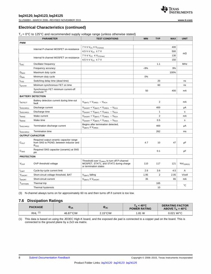
7.7 Typical CharacteristicsSee Figure 17 for a 1-cell application test circuit schematic and Figure 21 for the standalone cells application test circuitsschematic.
Figure 2. Efficiency 2-CellsFigure 1. Efficiency 1-Cell
Figure 3. Switching Waveforms in Fast Charge Mode Figure 4. Switching Waveforms in Voltage Regulation Mode
Figure 6. Soft Start WaveformsFigure 5. Dead Time
Copyright © 2006–2015, Texas Instruments Incorporated Submit Documentation Feedback 9
Product Folder Links: bq24120 bq24123 bq24125

-10
0
10
20
30
40
50
60
30M 50M 70M 100M 200M 300M 500M 700M 1G
Frequency [Hz]
Le
ve
l [d
BV
]μ
bq24120, bq24123, bq24125SLUS688H –MARCH 2006–REVISED NOVEMBER 2015 www.ti.com
Typical Characteristics (continued)See Figure 17 for a 1-cell application test circuit schematic and Figure 21 for the standalone cells application test circuitsschematic.
16 V, 1 A
Figure 7. Typical Radiated EMI Performance Measured on EVM
10 Submit Documentation Feedback Copyright © 2006–2015, Texas Instruments Incorporated
Product Folder Links: bq24120 bq24123 bq24125
UDG-04037
VLOW
Charge Voltage
Charge Current
Regulation V oltage
Regulation Current
VSHORT
Voltage Regulation andCharge Termination Phase
PrechargeTimer
ProgrammableSafety Timer
Current Regulation PhasePrecharge
Phase
Prechargeand Termination
ISHORT
bq24120, bq24123, bq24125www.ti.com SLUS688H –MARCH 2006–REVISED NOVEMBER 2015
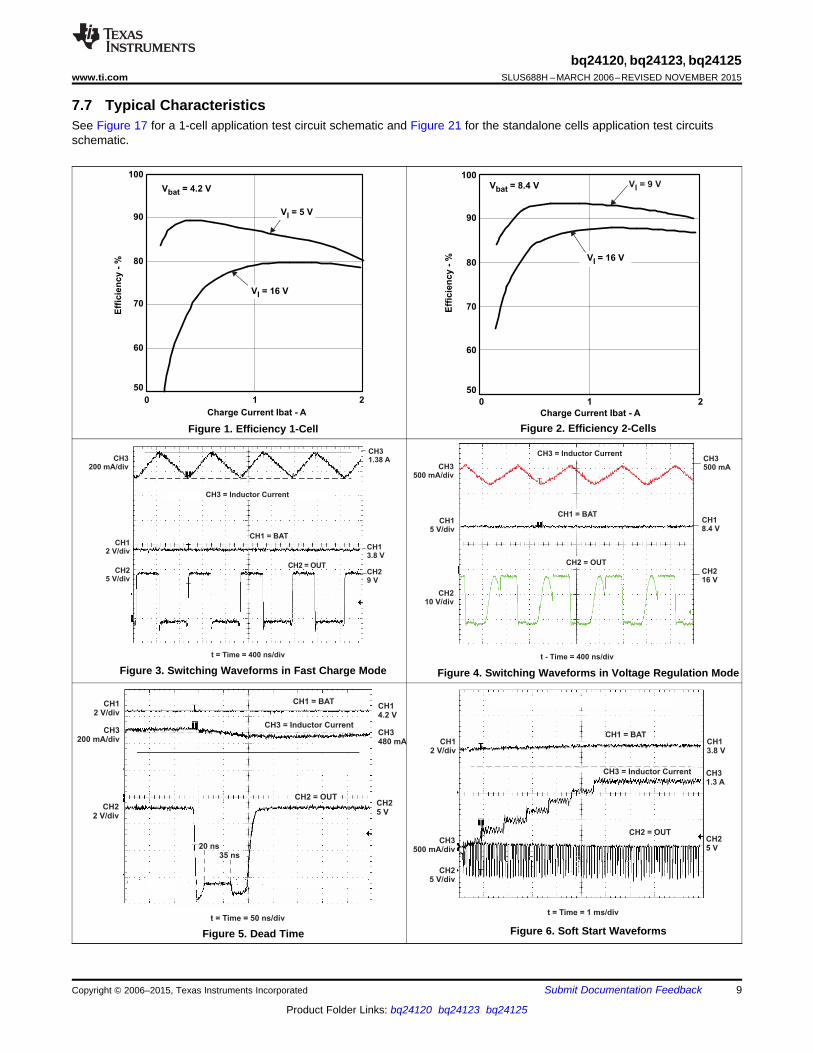
8 Detailed Description
8.1 OverviewThe bqSWITCHER supports a precision Li-ion or Li-polymer charging system for single cell or two cellapplications. See Figure 16 and Figure 8 for a typical charge profile.
The bq2412X has enhanced EMI performance that helps minimize the number of components needed to meetthe FCC-B Standard. The rise time of the OUT pin was slowed down to minimize the radiated EMI.
Figure 8. Typical Charging Profile
Copyright © 2006–2015, Texas Instruments Incorporated Submit Documentation Feedback 11
Product Folder Links: bq24120 bq24123 bq24125

PG
STAT1
STAT2
VSS
TS
PGND
CE
OUT
OUT
PGND
SNS
BAT
CELLS (bq24123)
FB (bq24125)
N/C (bq24120)
ISET1
ISET2
VCC
VCC
TTC
VCC
0.5V
VCC
1V
TIMER CLK
0.25V DSABL_TERM
0.75V
TIMER
FF CHAIN
PRE-CHG
TIMEOUT
FAST CHG
TIMEOUT
RESET
bqSWITCHER
bq2410x
VTSB
VTSB
LTF
HTF
TCO
RSET2
RSET1
INVIN
VTSB
VCC
IN
VoltageReference
VTSB VCC-6V
UVLO/PORVuvlo
POR
2.1V
+-
1V
+-
0.1V
1k+
-+-
+-
Ibat Reg
Vbat RegVCC
VCC
20uA
2.1V
+-
VCC
20uA
1VBAT
FBSPIN
1C
2C
VTSB
VTSB
MODOSC
S
RQ
Q
SUSPEND
UVLO/POR
TIMEOUT F AULT
TERM
PkILim or OVP
RAMP
VCC
I VCC/10
(Vpp=VCC/10)
RAMP
MOD
VCC
VCC-6V
6V
TG
BGSYNCH
COMPENSA TION
10
to FB
Co
Lo
10 F
Rsns
+
Pack+
Pack-
Temp
SLEEP VCC
BAT+ -
50 mV
TEMP
SUSPEND
SUSPEND
TSSPIN
TERMSLEEP
SUSPEND
OVP
Charge
TERM
BAT
Vreg
VCC
Discharge
Charge
Wake
SNS+
BAT_PRS_dischg
2.1V
Vrch
LowV
VSHORT
30msDgltch
BAT
30msDgltch
VovpOVP
CONTROL
LOGIC
(STATE
MACHINE)
OVP
TIMEOUT
SUSPEND
UVLO/POR
Vrch
Term_Det
LowV
BAT_PRS_disch
VSHORT
PkILim
SYNCH
SLEEP
Protection PMOS FET is OFF when not charging
or in SLEEP to prevent discharge of batterywhen IN < BAT
CE
IsynchSynch
V(150 mA)
BGTG
CHARGE
DISCHARGE
WAKE
PRE-CHARGE
FASTCHGDisable
PRE-CHG
Disable
+-
FASTCHGDisable
BAT
-1k
+SNS
Term_Det
0.1V30msdgltch
GateDrive FB
SPINONLY
CLAMP
Icntrl
PkILim
V(3.6A)
Sense FET
Sense FET
VCC
VCC-6V
PG
SLEEP
CHARGEPoff
FB
Term &
Timer
Disable
H
*
*Patent Pending #36889
bq24120, bq24123, bq24125SLUS688H –MARCH 2006–REVISED NOVEMBER 2015 www.ti.com
8.2 Functional Block Diagram
12 Submit Documentation Feedback Copyright © 2006–2015, Texas Instruments Incorporated
Product Folder Links: bq24120 bq24123 bq24125

RT2 =
V RTH RTHO(VTSB) COLD HOT´ ´ ´1
VLTF
1
VHTF
-
RTHHOT ´ - ´RTHCOLD
VO(VTSB)
HTFV- 1( ) VO(VTSB)
LTFV- 1( )
1
RT2
1
RTHCOLD
+
VO(VTSB)
LTFV- 1
RT1 =
Where:
V = V % / 100LTF O(VTSB) LTF 100¸
V = V % / 100HTF O(VTSB) HTF 100¸
´
´
bq24120, bq24123, bq24125www.ti.com SLUS688H –MARCH 2006–REVISED NOVEMBER 2015
8.3 Feature Description
8.3.1 PWM ControllerThe bq2412X provides an integrated fixed 1MHz frequency voltage-mode controller with Feed-Forward functionto regulate charge current or voltage. This type of controller is used to help improve line transient response,thereby simplifying the compensation network used for both continuous and discontinuous current conductionoperation. The voltage and current loops are internally compensated using a Type-III compensation scheme thatprovides enough phase boost for stable operation, allowing the use of small ceramic capacitors with very lowESR. There is a 0.5V offset on the bottom of the PWM ramp to allow the device to operate between 0% to 100%duty cycle.
The internal PWM gate drive can directly control the internal PMOS and NMOS power MOSFETs. The high-sidegate voltage swings from VCC (when off), to VCC-6 (when on and VCC is greater than 6V) to help reduce theconduction losses of the converter by enhancing the gate an extra volt beyond the standard 5V. The low-sidegate voltage swings from 6V, to turn on the NMOS, down to PGND to turn it off. The bq2412X has two back toback common-drain P-MOSFETs on the high side. An input P-MOSFET prevents battery discharge when IN islower than BAT. The second P-MOSFET behaves as the switching control FET, eliminating the need of abootstrap capacitor.
Cycle-by-cycle current limit is sensed through the internal high-side sense FET. The threshold is set to a nominal3.6A peak current. The low-side FET also has a current limit that decides if the PWM Controller will operate insynchronous or non-synchronous mode. This threshold is set to 100mA and it turns off the low-side NMOSbefore the current reverses, preventing the battery from discharging. Synchronous operation is used when thecurrent of the low-side FET is greater than 100mA to minimize power losses.
8.3.2 Temperature QualificationThe bqSWITCHER continuously monitors battery temperature by measuring the voltage between the TS pin andVSS pin. A negative temperature coefficient thermistor (NTC) and an external voltage divider typically developthis voltage. The bqSWITCHER compares this voltage against its internal thresholds to determine if charging isallowed. To initiate a charge cycle, the battery temperature must be within the V(LTF)-to-V(HTF) thresholds. Ifbattery temperature is outside of this range, the bqSWITCHER suspends charge and waits until the batterytemperature is within the V(LTF)-to-V(HTF) range. During the charge cycle (both precharge and fast charge), thebattery temperature must be within the V(LTF)-to-V(TCO) thresholds. If battery temperature is outside of this range,the bqSWITCHER suspends charge and waits until the battery temperature is within the V(LTF)-to-V(HTF) range.The bqSWITCHER suspends charge by turning off the PWM and holding the timer value (that is, timers are notreset during a suspend condition). Note that the bias for the external resistor divider is provided from the VTSBoutput. Applying a constant voltage between the V(LTF)-to-V(HTF) thresholds to the TS pin disables thetemperature-sensing feature.
(1)
Copyright © 2006–2015, Texas Instruments Incorporated Submit Documentation Feedback 13
Product Folder Links: bq24120 bq24123 bq24125

ISET1 ISET1ISET1
SNS CHARGE
K VR
R I
´
=
´
R(SNS)VIREG
IOCHARGE
IO(PRECHG) K(ISET2) V(ISET2)
R(ISET2) R(SNS)
Charge Suspend
Temperature Range
to Initiate Charge
Charge SuspendCharge Suspend
Temperature Range
During Charge Cycle
Charge Suspend
V(LTF)
V(HTF)
V(TCO)
VSS
VCC
bq24120, bq24123, bq24125SLUS688H –MARCH 2006–REVISED NOVEMBER 2015 www.ti.com
Feature Description (continued)
Figure 9. TS Pin Thresholds
8.3.3 Battery Preconditioning (Precharge)On power up, if the battery voltage is below the VLOWV threshold, the bqSWITCHER applies a precharge current,IPRECHG, to the battery. This feature revives deeply discharged cells. The bqSWITCHER activates a safety timer,tPRECHG, during the conditioning phase. If the VLOWV threshold is not reached within the timer period, thebqSWITCHER turns off the charger and enunciates FAULT on the STATx pins. In the case of a FAULTcondition, the bqSWITCHER reduces the current to IDETECT. IDETECT is used to detect a battery replacementcondition. Fault condition is cleared by POR or battery replacement.
The magnitude of the precharge current, IO(PRECHG), is determined by the value of programming resistor, R(ISET2),connected to the ISET2 pin.
where• RSNS is the external current-sense resistor• V(ISET2) is the output voltage of the ISET2 pin• K(ISET2) is the V/A gain factor• V(ISET2) and K(ISET2) are specified in the Electrical Characteristics table. (2)
8.3.4 Battery Charge CurrentThe battery charge current, IO(CHARGE), is established by setting the external sense resistor, R(SNS), and theresistor, R(ISET1), connected to the ISET1 pin.
In order to set the current, first choose R(SNS) based on the regulation threshold VIREG across this resistor. Thebest accuracy is achieved whe the VIREG is between 100mV and 200mV.
(3)
If the results is not a standard sense resistor value, choose the next larger value. Using the selected standardvalue, solve for VIREG. Once the sense resistor is selected, the ISET1 resistor can be calculated using thefollowing equation:
(4)
14 Submit Documentation Feedback Copyright © 2006–2015, Texas Instruments Incorporated
Product Folder Links: bq24120 bq24123 bq24125
tCHARGE C(TTC) K(TTC)
ITERM K(ISET2) VTERM
R(ISET2) R(SNS)
bq24120, bq24123, bq24125www.ti.com SLUS688H –MARCH 2006–REVISED NOVEMBER 2015
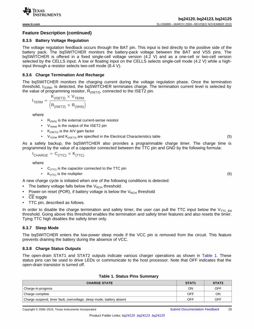
Feature Description (continued)8.3.5 Battery Voltage RegulationThe voltage regulation feedback occurs through the BAT pin. This input is tied directly to the positive side of thebattery pack. The bqSWITCHER monitors the battery-pack voltage between the BAT and VSS pins. ThebqSWITCHER is offered in a fixed single-cell voltage version (4.2 V) and as a one-cell or two-cell versionselected by the CELLS input. A low or floating input on the CELLS selects single-cell mode (4.2 V) while a high-input through a resistor selects two-cell mode (8.4 V).
8.3.6 Charge Termination And RechargeThe bqSWITCHER monitors the charging current during the voltage regulation phase. Once the terminationthreshold, ITERM, is detected, the bqSWITCHER terminates charge. The termination current level is selected bythe value of programming resistor, R(ISET2), connected to the ISET2 pin.
where• R(SNS) is the external current-sense resistor• VTERM is the output of the ISET2 pin• K(ISET2) is the A/V gain factor• VTERM and K(ISET2) are specified in the Electrical Characteristics table (5)
As a safety backup, the bqSWITCHER also provides a programmable charge timer. The charge time isprogrammed by the value of a capacitor connected between the TTC pin and GND by the following formula:
where• C(TTC) is the capacitor connected to the TTC pin• K(TTC) is the multiplier (6)
A new charge cycle is initiated when one of the following conditions is detected:• The battery voltage falls below the VRCH threshold.• Power-on reset (POR), if battery voltage is below the VRCH threshold• CE toggle• TTC pin, described as follows.
In order to disable the charge termination and safety timer, the user can pull the TTC input below the VTTC_ENthreshold. Going above this threshold enables the termination and safety timer features and also resets the timer.Tying TTC high disables the safety timer only.
8.3.7 Sleep ModeThe bqSWITCHER enters the low-power sleep mode if the VCC pin is removed from the circuit. This featureprevents draining the battery during the absence of VCC.
8.3.8 Charge Status OutputsThe open-drain STAT1 and STAT2 outputs indicate various charger operations as shown in Table 1. Thesestatus pins can be used to drive LEDs or communicate to the host processor. Note that OFF indicates that theopen-drain transistor is turned off.
Table 1. Status Pins SummaryCHARGE STATE STAT1 STAT2
Charge-in-progress ON OFFCharge complete OFF ONCharge suspend, timer fault, overvoltage, sleep mode, battery absent OFF OFF
Copyright © 2006–2015, Texas Instruments Incorporated Submit Documentation Feedback 15
Product Folder Links: bq24120 bq24123 bq24125

bq24120, bq24123, bq24125SLUS688H –MARCH 2006–REVISED NOVEMBER 2015 www.ti.com
8.3.9 PG OutputThe open-drain PG (power good) indicates when the AC-to-DC adapter (that is, VCC) is present. The output turnson when sleep-mode exit threshold, VSLP-EXIT, is detected. This output is turned off in the sleep mode. The PG pincan be used to drive an LED or communicate to the host processor.
8.3.10 CE Input (Charge Enable)The CE digital input is used to disable or enable the charge process. A low-level signal on this pin enables thecharge and a high-level VCC signal disables the charge. A high-to-low transition on this pin also resets all timersand fault conditions. Note that the CE pin should not be tied to VTSB. This may create power-up issues.
8.3.11 Timer Fault RecoveryAs shown in Figure 16, bqSWITCHER provides a recovery method to deal with timer fault conditions. Thefollowing summarizes this method.
Condition 1 VI(BAT) above recharge threshold (VOREG - VRCH) and timeout fault occurs.
Recovery method: bqSWITCHER waits for the battery voltage to fall below the recharge threshold. This couldhappen as a result of a load on the battery, self-discharge or battery removal. Once the battery falls below therecharge threshold, the bqSWITCHER clears the fault and enters the battery absent detection routine. A POR orCE toggle also clears the fault.
Condition 2 Charge voltage below recharge threshold (VOREG – VRCH) and timeout fault occurs
Recovery method: Under this scenario, the bqSWITCHER applies the IDETECT current. This small current is usedto detect a battery removal condition and remains on as long as the battery voltage stays below the rechargethreshold. If the battery voltage goes above the recharge threshold, then the bqSWITCHER disables the IDETECTcurrent and executes the recovery method described in Condition 1. Once the battery falls below the rechargethreshold, the bqSWITCHER clears the fault and enters the battery absent detection routine. A POR or CE togglealso clears the fault.
8.3.12 Output Overvoltage Protection (Applies to All Versions)The bqSWITCHER provides a built-in overvoltage protection to protect the device and other components againstdamages if the battery voltage gets too high, as when the battery is suddenly removed. When an overvoltagecondition is detected, this feature turns off the PWM and STATx pins. The fault is cleared once VIBAT drops to therecharge threshold (VOREG - VRCH).
8.3.13 Battery DetectionFor applications with removable battery packs, bqSWITCHER provides a battery absent detection scheme toreliably detect insertion and/or removal of battery packs.
16 Submit Documentation Feedback Copyright © 2006–2015, Texas Instruments Incorporated
Product Folder Links: bq24120 bq24123 bq24125
No
Yes
Yes
BATTERYPRESENT,
Begin Charge
NoBATTERYPRESENT,
Begin Charge
BATTERYABSENT
Yes
Enable I(DETECT)
for t(DETECT)
VI(BAT)<V(SHORT)
Apply I(WAKE)for t(WAKE)
POR or VRCH
Detection routine runs on power upand if VBAT drops below refreshthreshold due to removing batteryor discharging battery.
VI(BAT) >VO(REG)−VRCH
bq24120, bq24123, bq24125www.ti.com SLUS688H –MARCH 2006–REVISED NOVEMBER 2015
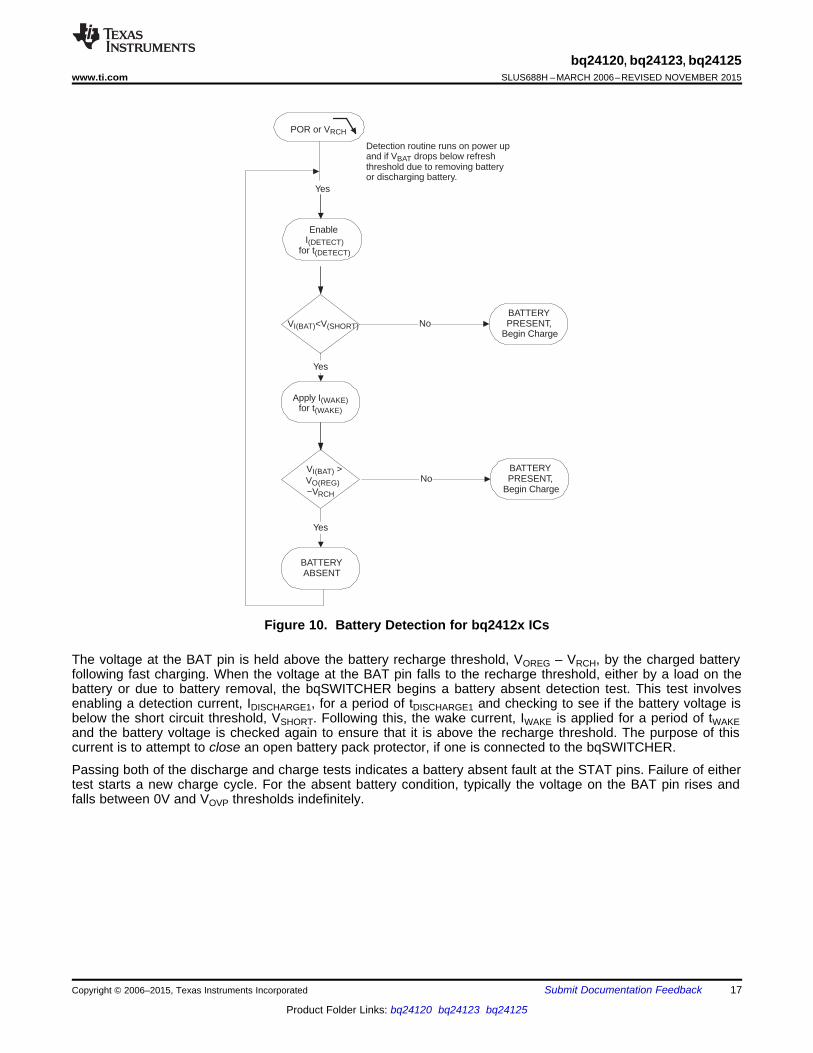
Figure 10. Battery Detection for bq2412x ICs
The voltage at the BAT pin is held above the battery recharge threshold, VOREG – VRCH, by the charged batteryfollowing fast charging. When the voltage at the BAT pin falls to the recharge threshold, either by a load on thebattery or due to battery removal, the bqSWITCHER begins a battery absent detection test. This test involvesenabling a detection current, IDISCHARGE1, for a period of tDISCHARGE1 and checking to see if the battery voltage isbelow the short circuit threshold, VSHORT. Following this, the wake current, IWAKE is applied for a period of tWAKEand the battery voltage is checked again to ensure that it is above the recharge threshold. The purpose of thiscurrent is to attempt to close an open battery pack protector, if one is connected to the bqSWITCHER.
Passing both of the discharge and charge tests indicates a battery absent fault at the STAT pins. Failure of eithertest starts a new charge cycle. For the absent battery condition, typically the voltage on the BAT pin rises andfalls between 0V and VOVP thresholds indefinitely.
Copyright © 2006–2015, Texas Instruments Incorporated Submit Documentation Feedback 17
Product Folder Links: bq24120 bq24123 bq24125
( )
( )
WAKE WAKEMAX _ WAKE
OREG RCH
MAX _ WAKE
MAX _ WAKE
I tC
V V 0 V
2 mA 0.5 sC
4.2 V 0.1 V 0 V
C 244 F
´=
- -
´=
- -
= m
DISCHRG1 DISCHRG1MAX _DIS
OREG SHORT
MAX _DIS
MAX _DIS
I tC
V V
400 A 1sC
4.2 V 2 V
C 182 F
´=
-
m ´=
-
= m
tWAKEtDISCHRG1
VOREG
2V/cell
IWAKE
- IDISCHRG1
Yes
Battery
Detected
No
Battery
Detected
No
Battery
Detected
Battery
Connected
VBAT
IBAT
tDISCHRG1
bq24120, bq24123, bq24125SLUS688H –MARCH 2006–REVISED NOVEMBER 2015 www.ti.com
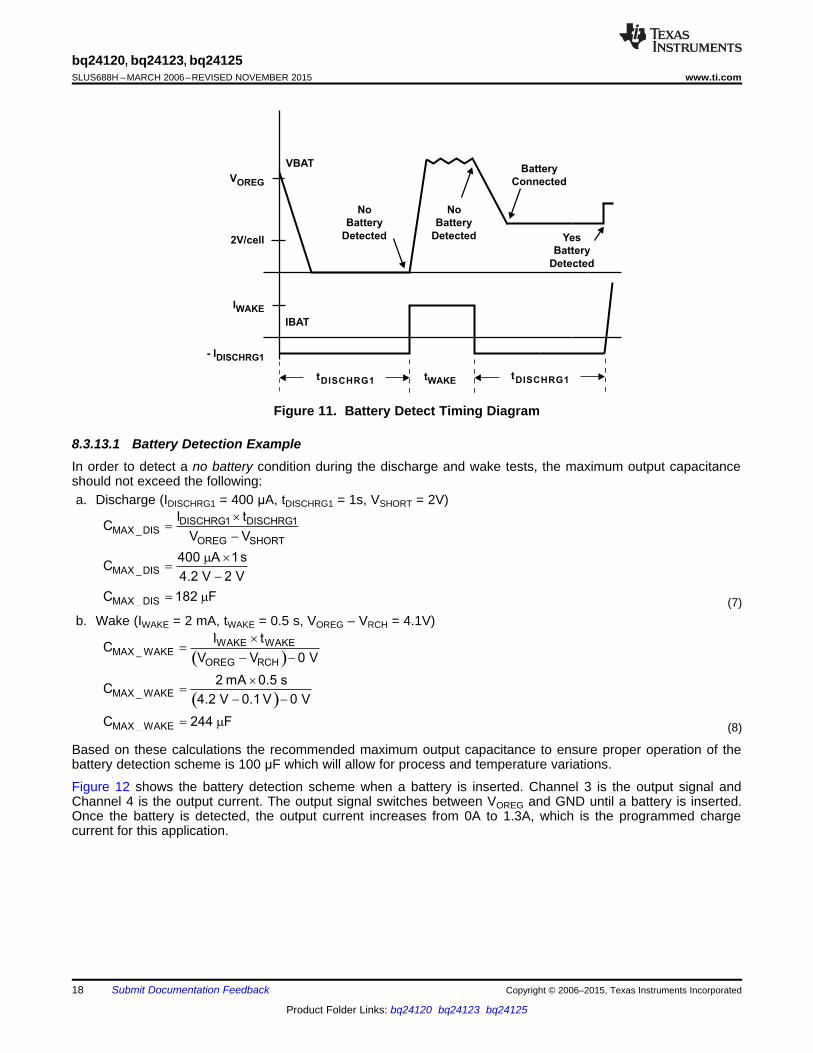
Figure 11. Battery Detect Timing Diagram
8.3.13.1 Battery Detection ExampleIn order to detect a no battery condition during the discharge and wake tests, the maximum output capacitanceshould not exceed the following:a. Discharge (IDISCHRG1 = 400 μA, tDISCHRG1 = 1s, VSHORT = 2V)
(7)b. Wake (IWAKE = 2 mA, tWAKE = 0.5 s, VOREG – VRCH = 4.1V)
(8)
Based on these calculations the recommended maximum output capacitance to ensure proper operation of thebattery detection scheme is 100 μF which will allow for process and temperature variations.
Figure 12 shows the battery detection scheme when a battery is inserted. Channel 3 is the output signal andChannel 4 is the output current. The output signal switches between VOREG and GND until a battery is inserted.Once the battery is detected, the output current increases from 0A to 1.3A, which is the programmed chargecurrent for this application.
18 Submit Documentation Feedback Copyright © 2006–2015, Texas Instruments Incorporated
Product Folder Links: bq24120 bq24123 bq24125
bq24120, bq24123, bq24125www.ti.com SLUS688H –MARCH 2006–REVISED NOVEMBER 2015
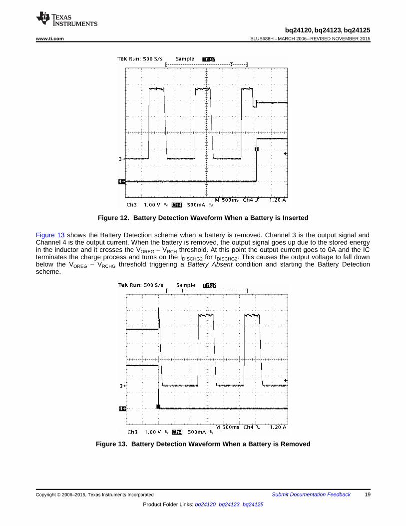
Figure 12. Battery Detection Waveform When a Battery is Inserted
Figure 13 shows the Battery Detection scheme when a battery is removed. Channel 3 is the output signal andChannel 4 is the output current. When the battery is removed, the output signal goes up due to the stored energyin the inductor and it crosses the VOREG – VRCH threshold. At this point the output current goes to 0A and the ICterminates the charge process and turns on the IDISCHG2 for tDISCHG2. This causes the output voltage to fall downbelow the VOREG – VRCHG threshold triggering a Battery Absent condition and starting the Battery Detectionscheme.
Figure 13. Battery Detection Waveform When a Battery is Removed
Copyright © 2006–2015, Texas Instruments Incorporated Submit Documentation Feedback 19
Product Folder Links: bq24120 bq24123 bq24125

CH3 = Inductor Current
CH2
10 V/div
CH2
16 V
CH1
200 mV/div
CH3
500 mA/div
CH3
0 A
CH1
0 V
CH1 = ISET2
CH2 = OUT
t = Time = 200 s/divm
ISET2 (ISET2)CHARGE
SNS ISET2
V KI
R R
´
=
´
+
-
FASTCHG
Disable
BAT
-
KISET2
+
+
ISET2
RISET2
RSNS
OUT
-
I CH
AR
GE
SNS
bq24120, bq24123, bq24125SLUS688H –MARCH 2006–REVISED NOVEMBER 2015 www.ti.com
8.3.14 Current Sense AmplifierBQ2412X family offers a current sense amplifier feature that translates the charge current into a DC voltage.Figure 14 is a block diagram of this feature.
Figure 14. Current Sense Amplifier
The voltage on the ISET2 pin can be used to calculate the charge current. Equation 9 shows the relationshipbetween the ISET2 voltage and the charge current:
(9)
This feature can be used to monitor the charge current during the current regulation phase (Fastcharge only) andthe voltage regulation phase. The schematics for the application circuit for this waveform is shown in Figure 21
Figure 15. Current Sense Amplifier
20 Submit Documentation Feedback Copyright © 2006–2015, Texas Instruments Incorporated
Product Folder Links: bq24120 bq24123 bq24125

Battery
Detected?
TS pin
in LTF to HTF
range?Indicate CHARGE
SUSPEND
No
VBAT <VLOWV Yes
No
VBAT<VLOWV
T30min
Expired?No
Yes
Indicate Fault
Battery
Replaced?
VBAT< VOREG -
VRCH ?
No
Yes
FSTCHG timer
Expired?
No
Suspend charge
Indicate Charge-
In-Progress
Regulate
IPRECHG
Indicate Charge-
In-Progress
Regulate
Current or Voltage
Indicate BATTERY
ABSENT
Check for battery
Presence
No
Reset and Start
T30min timer
TS pin
in LTF to TCO
range?Indicate CHARGE
SUSPEND
No
Suspend charge
POR
Yes
Yes
Reset and Start
FSTCHG timer
TS pin
in LTF to TCO
range?
ITERM detection?
Yes
Yes
VBAT< VOREG -VRCH?
NoIndicate DONE
Charge Complete
Yes
VBAT<VLOWV
No
No
- Fault Condition
No
Yes
Yes
TS pin
in LTF to HTF
range?
No
TS pin
in LTF to HTF
range?
Indicate CHARGE
SUSPEND
Suspend charge
No
No
Indicate Charge-
In-Progress
- Turn off charge
- Enable I DISCHG2for tDISCHG2
Indicate BATTERY
ABSENT
Battery Removed
Yes
Yes
Yes
VBAT> VOREG -VRCH ?
Indicate Fault
- Fault Condition
- Enable I DETECT
No
Yes
VBAT> VOREG --
VRCH ?
No
Indicate Fault
- Disable I DETECT
Yes
Yes
bq24120, bq24123, bq24125www.ti.com SLUS688H –MARCH 2006–REVISED NOVEMBER 2015
8.4 Device Functional ModesFigure 16 shows the operational flow chart for a typical charge operation.
Figure 16. Operational Flow Chart
Copyright © 2006–2015, Texas Instruments Incorporated Submit Documentation Feedback 21
Product Folder Links: bq24120 bq24123 bq24125

3 IN
4 IN
6 VCC
2 STAT1
19 STAT2
5 PG
7 TTC
16 CE
10 VSS
13 NC
OUT 1
OUT 20
PGND 17
PGND 18
SNS 15
BAT 14
ISET1 8
ISET2 9
TS 12
VTSB 11
VIN
10mF10mH
LO
CIN
COUT
RSNS
0.1W1.5 KW 1.5 KW 1.5 KW
ChargeDoneAdapterPresent
7.5 KW
7.5 KW
0.1 Fm
9.31 KW
442 KW
VTSB
RT1
RT2
R
R
ISET1
ISET2
103AT
Battery
Pack
Pack-
Pack+
0.1 Fm0.1 Fm
0.1 Fm
10 Fm
CTTC
BQ24120
0.1 Fm0.1 Fm
MMBZ18VALT1
(See Note)
bq24120, bq24123, bq24125SLUS688H –MARCH 2006–REVISED NOVEMBER 2015 www.ti.com
9 Application and Implementation
NOTEInformation in the following applications sections is not part of the TI componentspecification, and TI does not warrant its accuracy or completeness. TI’s customers areresponsible for determining suitability of components for their purposes. Customers shouldvalidate and test their design implementation to confirm system functionality.
9.1 Application InformationThe bq2412x battery charger supports precision Li-ion or Li-polymer charging system for single cell or two cellapplication. The design example below shows the design consideration for a 1-cell application.
9.2 Typical Application
TVS Zener diode is optional for devices with date codes effective March 2008
Figure 17. Standalone 1-Cell Application
9.2.1 Design RequirementsFor this design example, use the parameters listed in Table 2.
Table 2. Design ParametersDESIGN PARAMETER EXAMPLE VALUE
AC adapter voltage (VIN) 16 VBattery charge voltage (number of cells in series) 4.2 V (1 cell)Battery charge current (during fast charge phase) 1.33 APrecharge and termination current 0.133 ASafety timer 5 hoursInductor ripple current 30% of fast charge current (0.4 A)Charging temperature range 0°C to 45°C
22 Submit Documentation Feedback Copyright © 2006–2015, Texas Instruments Incorporated
Product Folder Links: bq24120 bq24123 bq24125

RSNSSNS
CHARGE
VR
I=
o
OUT OUT
OUT 2 2o OUT
OUT 2 3 2 6
OUT
1ƒ
2 L C
1C
4 ƒ L
1C
4 (16 10 ) (10 10 )
C 9.89 F
-
=
p ´
=
p ´ ´
=
p ´ ´ ´ ´
= m
LLPK OUT
LPK
LPK
II I
2
0.282I 1.33
2
I 1.471 A
D= +
= +
=
( )
BAT INMAX BATL
INMAX OUT
L 6 6
L
V (V V )I
V ƒ L
4.2 (16 4.2)I
(16 1.1 10 ) 10 10
I 0.282 A
-
´ -D =
´ ´
´ -D =
´ ´ ´ ´
D =
( )
( )
( )
L CHARGE CHARGE
BAT INMAX BATOUT
INMAX L
OUT 6
OUT
I I I Ripple
V V VL
V ƒ I
4.2 16 4.2L
16 (1.1 10 ) 1.33 0.3
L 7.06 H
D = ´
´ -=
´ ´ D
´ -=
´ ´ ´ ´
= m
bq24120, bq24123, bq24125www.ti.com SLUS688H –MARCH 2006–REVISED NOVEMBER 2015
9.2.2 Detailed Design ProcedureThis section provides a detailed system design example for the bq24120.• VIN = 16V• VBAT = 4.2V (1-Cell)• ICHARGE = 1.33 A• IPRECHARGE = ITERM = 133 mA• Safety Timer = 5.0 hours• Inductor Ripple Current = 30% of Fast Charge Current• Initiate Charge Temperature = 0°C to 45°C1. Determine the inductor value (LOUT) for the specified charge current ripple:
(10)
Set the output inductor to standard 10 μH. Calculate the total ripple current with using the 10 μH inductor:
(11)
Calculate the maximum output current (peak current):
(12)
Use standard 10 μH inductor with a saturation current higher than 1.471A. (that is, Sumida CDRH74-100)2. Determine the output capacitor value (COUT) using 16 kHz as the resonant frequency:
(13)
Use standard value 10 μF, 25V, X5R, ±20% ceramic capacitor (that is, Panasonic 1206 ECJ-3YB1E106M)3. Determine the sense resistor using the following equation:
(14)
In order to get better current regulation accuracy (±10%), let VRSNS be between 100 mV and 200 mV. UseVRSNS = 100 mV and calculate the value for the sense resistor.
Copyright © 2006–2015, Texas Instruments Incorporated Submit Documentation Feedback 23
Product Folder Links: bq24120 bq24123 bq24125

TTC
TTC
TTC
tCHARGEC
KTTC
300 mC
2.6 m / nF
C 115.4 nF
=
=
=
ISET2 ISET2ISET2
SNS CHARGE
ISET2
ISET2
K VR
R I
1000 1.0R
0.1 1.33
R 7.5 k
´=
´
´=
´
= W
ISET1 ISET1ISET1
SNS CHARGE
ISET1
ISET1
K VR
R I
1000 1.0R
0.1 1.33
R 7.5 k
´=
´
´=
´
= W
2
RSNS CHARGE SNS
2
RSNS
RSNS
P I R
P 1.33 0.1
P 176.9 mW
= ´
= ´
=
SNS
SNS
100 mVR
1.33 A
R 0.075
=
= W
bq24120, bq24123, bq24125SLUS688H –MARCH 2006–REVISED NOVEMBER 2015 www.ti.com
(15)
This value is not standard in resistors. If this happens, then choose the next larger value which in this case is0.1Ω. Using the same equation (15) the actual VRSNS will be 133mV. Calculate the power dissipation on thesense resistor:
(16)
Select standard value 100 mΩ, 0.25W 0805, 1206 or 2010 size, high precision sensing resistor. (that is,Vishay CRCW1210-0R10F)
4. Determine ISET 1 resistor using the following equation:
(17)
Select standard value 7.5 kΩ, 1/16W ±1% resistor (that is, Vishay CRCWD0603-7501-F)5. Determine ISET 2 resistor using the following equation:
(18)
Select standard value 7.5 kΩ, 1/16W ±1% resistor (that is, Vishay CRCWD0603-7501-F)6. Determine TTC capacitor (CTTC) for the 5.0 hours safety timer using the following equation:
(19)
Select standard value 100 nF, 16V, X7R, ±10% ceramic capacitor (that is, Panasonic ECJ-1VB1C104K).Using this capacitor the actual safety timer will be 4.3 hours.
7. Determine TS resistor network for an operating temperature range from 0°C to 45°C.
24 Submit Documentation Feedback Copyright © 2006–2015, Texas Instruments Incorporated
Product Folder Links: bq24120 bq24123 bq24125
f0 12 LOUT COUT
COLD
HOT
RTH 27.28 k
RTH 4.912 k
RT1 9.31k
RT2 442 k
= W
= W
= W
= W
RT2 =
V RTH RTHO(VTSB) COLD HOT´ ´ ´1
VLTF
1
VHTF
-
RTHHOT ´ - ´RTHCOLD
VO(VTSB)
HTFV- 1( ) VO(VTSB)
LTFV- 1( )
1
RT2
1
RTHCOLD
+
VO(VTSB)
LTFV- 1
RT1 =
Where:
V = V % / 100LTF O(VTSB) LTF 100¸
V = V % / 100HTF O(VTSB) HTF 100¸
´
´
103AT
RT1
RT2
VTSB
TS
RTH
bq24120, bq24123, bq24125www.ti.com SLUS688H –MARCH 2006–REVISED NOVEMBER 2015
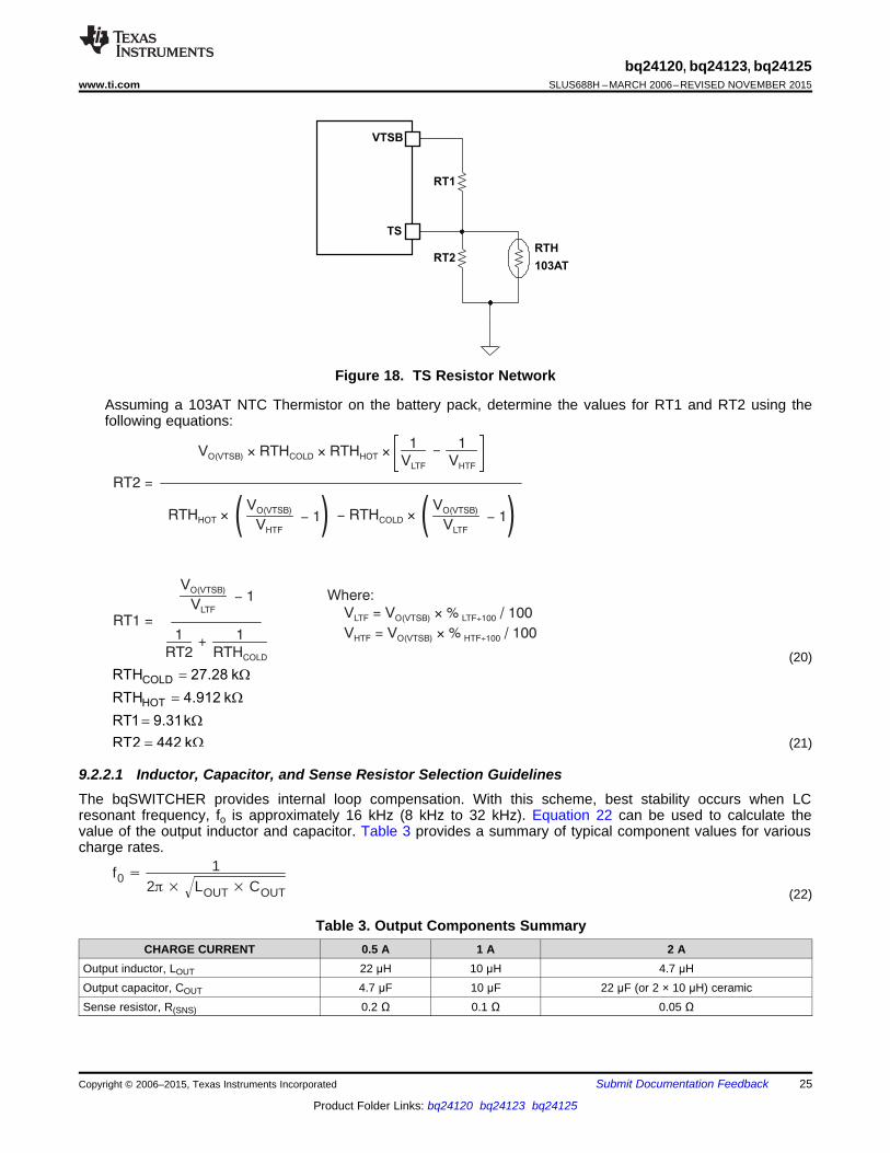
Figure 18. TS Resistor Network
Assuming a 103AT NTC Thermistor on the battery pack, determine the values for RT1 and RT2 using thefollowing equations:
(20)
(21)
9.2.2.1 Inductor, Capacitor, and Sense Resistor Selection GuidelinesThe bqSWITCHER provides internal loop compensation. With this scheme, best stability occurs when LCresonant frequency, fo is approximately 16 kHz (8 kHz to 32 kHz). Equation 22 can be used to calculate thevalue of the output inductor and capacitor. Table 3 provides a summary of typical component values for variouscharge rates.
(22)
Table 3. Output Components SummaryCHARGE CURRENT 0.5 A 1 A 2 A
Output inductor, LOUT 22 μH 10 μH 4.7 μHOutput capacitor, COUT 4.7 μF 10 μF 22 μF (or 2 × 10 μH) ceramicSense resistor, R(SNS) 0.2 Ω 0.1 Ω 0.05 Ω
Copyright © 2006–2015, Texas Instruments Incorporated Submit Documentation Feedback 25
Product Folder Links: bq24120 bq24123 bq24125

3 IN
4 IN
6 VCC
2 STAT1
19 STAT2
5 PG
7 TTC
16 CE
10 VSS
13 CELLS
OUT 1
OUT 20
PGND 17
PGND 18
SNS 15
BAT 14
ISET1 8
ISET2 9
TS 12
VTSB 11
VIN
10mF10 Hm
LO
CIN
C
C
R
R
OUT
TTC
T2
T1
RSNS
0.1W1.5 KW 1.5 KW 1.5 KW
10 Fm
0.1 Fm
0.1 Fm
0.1 Fm
0.1 Fm
ChargeDoneAdapterPresent
7.5 KW
7.5 KW9.31 KW
442 KW
VTSBRISET1
RISET2
103AT
Battery
Pack
Pack-
Pack+
10 KW
VIN
BQ24123
MMBZ18VALT1(See Note)
t = Time = 400 ns/div
CH2
9 V
CH3
1.38 A
CH1
3.8 V
CH2
5 V/div
CH3
200 mA/div
CH1
2 V/div
CH3 = Inductor Current
CH1 = BAT
CH2 = OUT
V = 4.2 Vbat
50
60
70
80
90
100
0 1 2
Charge Current Ibat - A
Eff
icie
nc
y -
%
V = 16 VI
V = 5 VI
bq24120, bq24123, bq24125SLUS688H –MARCH 2006–REVISED NOVEMBER 2015 www.ti.com
9.2.3 Application Curves
Figure 19. Efficiency 1-Cell Figure 20. Switching Waveforms in Fast Charge Mode
9.3 System Examples
TVS Zener diode is optional for devices with date codes effective March 2008
Figure 21. Standalone 2-Cells Application
26 Submit Documentation Feedback Copyright © 2006–2015, Texas Instruments Incorporated
Product Folder Links: bq24120 bq24123 bq24125

3 IN
4 IN
6 VCC
2 STAT1
19 STAT2
5 PG
7 TTC
16 CE
10 VSS
13 FB
OUT 1
OUT 20
PGND 17
PGND 18
SNS 15
BAT 14
ISET1 8
ISET2 9
TS 12
VTSB 11
VIN
L
CTTC
CIN COUT
RSNS
0.1W1.5 KW 1.5 KW 1.5 KW
ChargeDoneAdapterPresent
7.5 KW
20 KW9.31 KW
442 KW
RT1
103AT
BatteryPack
Pack-
Pack+
0.1 Fm
0.1 Fm
0.1 Fm
0.1 Fm
10 Fm10 Hm
10 Fm
BQ24125
RISET2
RISET1
200 KW
143 KW
RT2
VTSB
OUT
MMBZ18VALT1
D1
(See Note)
3 IN
4 IN
6 VCC
2 STAT1
19 STAT2
5 PG
7 TTC
16 CE
10 VSS
13 FB
OUT 1
OUT 20
PGND 17
PGND 18
SNS 15
BAT 14
ISET1 8
ISET2 9
TS 12
VTSB 11
VIN
L
CTTC
CIN COUT
RSNS
0.1W1.5 KW 1.5 KW 1.5 KW
ChargeDoneAdapterPresent
7.5 KW
7.5 KW9.31 KW
442 KW
RT1
103AT
BatteryPack
Pack-
Pack+
0.1 Fm
0.1 Fm
0.1 Fm
0.1 Fm
10 Fm10 Hm
10 Fm
BQ24125
RISET2
RISET1
100 KW
301 KW
RT2
VTSB
OUT
MMBZ18VALT1
D1
(See Note)
bq24120, bq24123, bq24125www.ti.com SLUS688H –MARCH 2006–REVISED NOVEMBER 2015
System Examples (continued)
Zener diode not needed for bq24125.
Figure 22. Externally Programmable Application
Using bq24125 to charge a LiFePO4 battery
Zener diode not needed for bq24125.
Figure 23. 1-Cell LiFePO4 Application
The LiFePO4 battery has many unique features such as a very high thermal runaway temperature, highdischarge current capability, and high charge current. These special features make it attractive in manyapplications such as power tools. The recommended charge voltage is 3.6 V and termination current is 50 mA.Figure 23 shows an application circuit for charging one cell LiFePO4 using bq24105. The charge voltage is 3.6 Vand recharge voltage is 3.516 V. The fast charging current is set to 1.33 A while the termination current is50 mA. This circuit can be easily changed to support two or three cell applications. However, only 84 mV
Copyright © 2006–2015, Texas Instruments Incorporated Submit Documentation Feedback 27
Product Folder Links: bq24120 bq24123 bq24125
3 IN
4 IN
6 VCC
2 STAT1
19 STAT2
5 PG
7 TTC
16 CE
10 VSS
13 NC
OUT 1
OUT 20
PGND 17
PGND 18
SNS 15
BAT 14
ISET1 8
ISET2 9
TS 12
VTSB 11
VIN
LO
CIN COUT
RSNS
0.1W1.5 KW 1.5 KW 1.5 KW
ChargeDoneAdapterPresent
7.5 KW
7.5 KW9.31 KW
442 KW
VTSB
103AT
BatteryPack
Pack-
Pack+
0.1 Fm
0.1 Fm
0.1 Fm
0.1 Fm
10 Fm10 Hm
10 Fm
BQ24120
RSYS
MMBZ18VALT1
(See Note)
bq24120, bq24123, bq24125SLUS688H –MARCH 2006–REVISED NOVEMBER 2015 www.ti.com
System Examples (continued)difference between regulation set point and rechargeable threshold makes it frequently enter into recharge modewhen small load current is applied. This can be solved by lower down the recharge voltage threshold to 200 mVto discharge more energy from the battery before it enters recharge mode again. See the application report,Using the bq24105/25 to Charge LiFePO4 Battery, SLUA443, for additional details. The recharge thresholdshould be selected according to real application conditions.
Figure 24 shows charging a battery and powering system without affecting battery charge and termination.
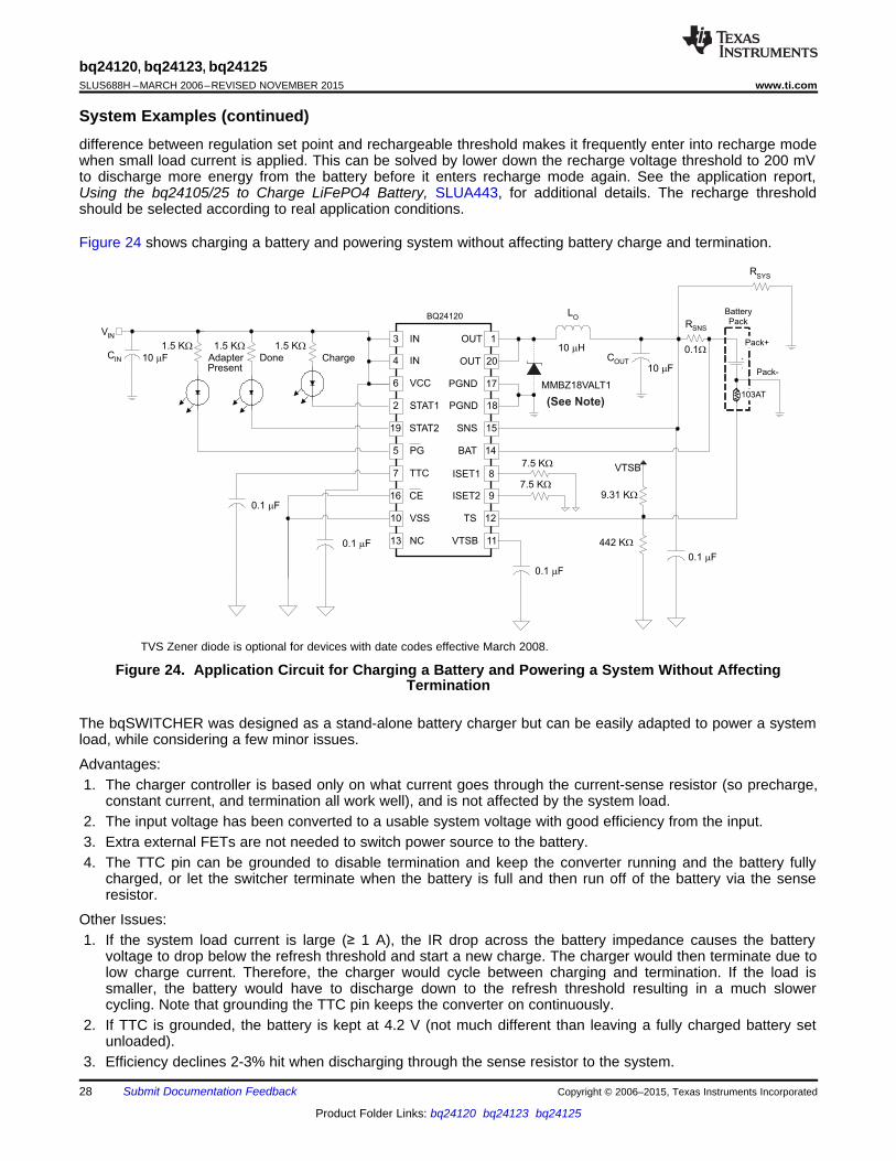
TVS Zener diode is optional for devices with date codes effective March 2008.
Figure 24. Application Circuit for Charging a Battery and Powering a System Without AffectingTermination
The bqSWITCHER was designed as a stand-alone battery charger but can be easily adapted to power a systemload, while considering a few minor issues.
Advantages:1. The charger controller is based only on what current goes through the current-sense resistor (so precharge,
constant current, and termination all work well), and is not affected by the system load.2. The input voltage has been converted to a usable system voltage with good efficiency from the input.3. Extra external FETs are not needed to switch power source to the battery.4. The TTC pin can be grounded to disable termination and keep the converter running and the battery fully
charged, or let the switcher terminate when the battery is full and then run off of the battery via the senseresistor.
Other Issues:1. If the system load current is large (≥ 1 A), the IR drop across the battery impedance causes the battery
voltage to drop below the refresh threshold and start a new charge. The charger would then terminate due tolow charge current. Therefore, the charger would cycle between charging and termination. If the load issmaller, the battery would have to discharge down to the refresh threshold resulting in a much slowercycling. Note that grounding the TTC pin keeps the converter on continuously.
2. If TTC is grounded, the battery is kept at 4.2 V (not much different than leaving a fully charged battery setunloaded).
3. Efficiency declines 2-3% hit when discharging through the sense resistor to the system.
28 Submit Documentation Feedback Copyright © 2006–2015, Texas Instruments Incorporated
Product Folder Links: bq24120 bq24123 bq24125

bq24120, bq24123, bq24125www.ti.com SLUS688H –MARCH 2006–REVISED NOVEMBER 2015
10 Power Supply RecommendationsFor proper operation of bq2421x, VCC and IN (tied together) must be from 4.35 V to 16 V. Power limit for theinput supply must be greater than the maximum power required for charging the battery (plus any additional loadon the output of the switch-mode converter).
11 Layout
11.1 Layout GuidelinesIt is important to pay special attention to the PCB layout. The following provides some guidelines:• To obtain optimal performance, the power input capacitors, connected from input to PGND, should be placed
as close as possible to the bqSWITCHER. The output inductor should be placed directly above the IC and theoutput capacitor connected between the inductor and PGND of the IC. The intent is to minimize the currentpath loop area from the OUT pin through the LC filter and back to the PGND pin. The sense resistor shouldbe adjacent to the junction of the inductor and output capacitor. Route the sense leads connected across theRSNS back to the IC, close to each other (minimize loop area) or on top of each other on adjacent layers. BATand SNS traces should be away from high di/dt traces such as the OUT pin. Use an optional capacitordownstream from the sense resistor if long (inductive) battery leads are used.
• Place all small-signal components (CTTC, RSET1/2 and TS) close to their respective IC pin (do not placecomponents such that routing interrupts power stage currents). All small control signals should be routedaway from the high current paths.
• The PCB should have a ground plane (return) connected directly to the return of all components through vias(3 vias per capacitor for power-stage capacitors, 3 vias for the IC PGND, 1 via per capacitor for small-signalcomponents). A star ground design approach is typically used to keep circuit block currents isolated (high-power/low-power small-signal) which reduces noise-coupling and ground-bounce issues. A single groundplane for this design gives good results. With this small layout and a single ground plane, there is not aground-bounce issue, and having the components segregated minimizes coupling between signals.
• The high-current charge paths into IN and from the OUT pins must be sized appropriately for the maximumcharge current in order to avoid voltage drops in these traces. The PGND pins should be connected to theground plane to return current through the internal low-side FET. The thermal vias in the IC PowerPAD™provide the return-path connection.
• The bqSWITCHER is packaged in a thermally enhanced MLP package. The package includes a thermal padto provide an effective thermal contact between the IC and the PCB. Full PCB design guidelines for thispackage are provided in the application report entitled: QFN/SON PCB Attachment, SLUA271. Six 10-13 milvias are a minimum number of recommended vias, placed in the IC's power pad, connecting it to a groundthermal plane on the opposite side of the PWB. This plane must be at the same potential as VSS and PGNDof this IC.
• See user's guide, Using the bq241xx (bqSWITCHER™), SLUU200 for an example of good layout.
Copyright © 2006–2015, Texas Instruments Incorporated Submit Documentation Feedback 29
Product Folder Links: bq24120 bq24123 bq24125

J A(JA)
T T
P
-q =
bq24120, bq24123, bq24125SLUS688H –MARCH 2006–REVISED NOVEMBER 2015 www.ti.com
11.2 Layout Example
Figure 25. bq2412x PCB Layout
11.3 Thermal ConsiderationsThe SWITCHER is packaged in a thermally enhanced MLP package. The package includes a thermal pad toprovide an effective thermal contact between the IC and the printed circuit board (PCB). Full PCB designguidelines for this package are provided in the application report entitled: QFN/SON PCB Attachment , SLUA271.
The most common measure of package thermal performance is thermal impedance (θJA) measured (or modeled)from the chip junction to the air surrounding the package surface (ambient). The mathematical expression for θJAis:
where• TJ = chip junction temperature• TA = ambient temperature• P = device power dissipation (23)
Factors that can greatly influence the measurement and calculation of θJA include:• Whether or not the device is board mounted• Trace size, composition, thickness, and geometry• Orientation of the device (horizontal or vertical)• Volume of the ambient air surrounding the device under test and airflow• Whether or not other surfaces are in close proximity to the device being tested
The device power dissipation, P, is a function of the charge rate and the voltage drop across the internal powerFET. It can be calculated from the following equation:
P = [Vin × lin - Vbat × Ibat]
Due to the charge profile of Li-xx batteries, the maximum power dissipation is typically seen at the beginning ofthe charge cycle when the battery voltage is at its lowest. (See Figure 8).
30 Submit Documentation Feedback Copyright © 2006–2015, Texas Instruments Incorporated
Product Folder Links: bq24120 bq24123 bq24125
bq24120, bq24123, bq24125www.ti.com SLUS688H –MARCH 2006–REVISED NOVEMBER 2015
12 Device and Documentation Support
12.1 Documentation Support
12.1.1 Related DocumentationFor related documentation, see the following:• Using the bq24105/25 to Charge LiFePO4 Battery, SLUA443• QFN/SON PCB Attachment , SLUA271• Using the bq241xx (bqSWITCHER™), SLUU200
12.2 Related LinksThe table below lists quick access links. Categories include technical documents, support and communityresources, tools and software, and quick access to sample or buy.
Table 4. Related LinksTECHNICAL TOOLS & SUPPORT &PARTS PRODUCT FOLDER SAMPLE & BUY DOCUMENTS SOFTWARE COMMUNITY
bq24120 Click here Click here Click here Click here Click herebq24123 Click here Click here Click here Click here Click herebq24125 Click here Click here Click here Click here Click here
12.3 Community ResourcesThe following links connect to TI community resources. Linked contents are provided "AS IS" by the respectivecontributors. They do not constitute TI specifications and do not necessarily reflect TI's views; see TI's Terms ofUse.
TI E2E™ Online Community TI's Engineer-to-Engineer (E2E) Community. Created to foster collaborationamong engineers. At e2e.ti.com, you can ask questions, share knowledge, explore ideas and helpsolve problems with fellow engineers.
Design Support TI's Design Support Quickly find helpful E2E forums along with design support tools andcontact information for technical support.
12.4 TrademarksbqSWITCHER, PowerPAD, E2E are trademarks of Texas Instruments.All other trademarks are the property of their respective owners.
12.5 Electrostatic Discharge CautionThese devices have limited built-in ESD protection. The leads should be shorted together or the device placed in conductive foamduring storage or handling to prevent electrostatic damage to the MOS gates.
12.6 GlossarySLYZ022 — TI Glossary.
This glossary lists and explains terms, acronyms, and definitions.
13 Mechanical, Packaging, and Orderable InformationThe following pages include mechanical, packaging, and orderable information. This information is the mostcurrent data available for the designated devices. This data is subject to change without notice and revision ofthis document. For browser-based versions of this data sheet, refer to the left-hand navigation.
Copyright © 2006–2015, Texas Instruments Incorporated Submit Documentation Feedback 31
Product Folder Links: bq24120 bq24123 bq24125

PACKAGE OPTION ADDENDUM
www.ti.com 15-Apr-2017
Addendum-Page 1
PACKAGING INFORMATION
Orderable Device Status(1)
Package Type PackageDrawing
Pins PackageQty
Eco Plan(2)
Lead/Ball Finish(6)
MSL Peak Temp(3)
Op Temp (°C) Device Marking(4/5)
Samples
BQ24120RHLR ACTIVE VQFN RHL 20 3000 Green (RoHS& no Sb/Br)
CU NIPDAU Level-2-260C-1 YEAR -40 to 85 BQU
BQ24120RHLRG4 ACTIVE VQFN RHL 20 3000 Green (RoHS& no Sb/Br)
CU NIPDAU Level-2-260C-1 YEAR -40 to 85 BQU
BQ24120RHLT ACTIVE VQFN RHL 20 250 Green (RoHS& no Sb/Br)
CU NIPDAU Level-2-260C-1 YEAR -40 to 85 BQU
BQ24123RHLR ACTIVE VQFN RHL 20 3000 Green (RoHS& no Sb/Br)
CU NIPDAU Level-2-260C-1 YEAR -40 to 85 BQV
BQ24123RHLRG4 ACTIVE VQFN RHL 20 3000 Green (RoHS& no Sb/Br)
CU NIPDAU Level-2-260C-1 YEAR -40 to 85 BQV
BQ24123RHLT ACTIVE VQFN RHL 20 250 Green (RoHS& no Sb/Br)
CU NIPDAU Level-2-260C-1 YEAR -40 to 85 BQV
BQ24123RHLTG4 ACTIVE VQFN RHL 20 250 Green (RoHS& no Sb/Br)
CU NIPDAU Level-2-260C-1 YEAR -40 to 85 BQV
BQ24125RHLR ACTIVE VQFN RHL 20 3000 Green (RoHS& no Sb/Br)
CU NIPDAU Level-2-260C-1 YEAR -40 to 125 CDZ
BQ24125RHLRG4 ACTIVE VQFN RHL 20 3000 Green (RoHS& no Sb/Br)
CU NIPDAU Level-2-260C-1 YEAR -40 to 125 CDZ
BQ24125RHLT ACTIVE VQFN RHL 20 250 Green (RoHS& no Sb/Br)
CU NIPDAU Level-2-260C-1 YEAR -40 to 125 CDZ
BQ24125RHLTG4 ACTIVE VQFN RHL 20 250 Green (RoHS& no Sb/Br)
CU NIPDAU Level-2-260C-1 YEAR -40 to 125 CDZ
(1) The marketing status values are defined as follows:ACTIVE: Product device recommended for new designs.LIFEBUY: TI has announced that the device will be discontinued, and a lifetime-buy period is in effect.NRND: Not recommended for new designs. Device is in production to support existing customers, but TI does not recommend using this part in a new design.PREVIEW: Device has been announced but is not in production. Samples may or may not be available.OBSOLETE: TI has discontinued the production of the device.
(2) Eco Plan - The planned eco-friendly classification: Pb-Free (RoHS), Pb-Free (RoHS Exempt), or Green (RoHS & no Sb/Br) - please check http://www.ti.com/productcontent for the latest availabilityinformation and additional product content details.TBD: The Pb-Free/Green conversion plan has not been defined.Pb-Free (RoHS): TI's terms "Lead-Free" or "Pb-Free" mean semiconductor products that are compatible with the current RoHS requirements for all 6 substances, including the requirement thatlead not exceed 0.1% by weight in homogeneous materials. Where designed to be soldered at high temperatures, TI Pb-Free products are suitable for use in specified lead-free processes.

PACKAGE OPTION ADDENDUM
www.ti.com 15-Apr-2017
Addendum-Page 2
Pb-Free (RoHS Exempt): This component has a RoHS exemption for either 1) lead-based flip-chip solder bumps used between the die and package, or 2) lead-based die adhesive used betweenthe die and leadframe. The component is otherwise considered Pb-Free (RoHS compatible) as defined above.Green (RoHS & no Sb/Br): TI defines "Green" to mean Pb-Free (RoHS compatible), and free of Bromine (Br) and Antimony (Sb) based flame retardants (Br or Sb do not exceed 0.1% by weightin homogeneous material)
(3) MSL, Peak Temp. - The Moisture Sensitivity Level rating according to the JEDEC industry standard classifications, and peak solder temperature.
(4) There may be additional marking, which relates to the logo, the lot trace code information, or the environmental category on the device.
(5) Multiple Device Markings will be inside parentheses. Only one Device Marking contained in parentheses and separated by a "~" will appear on a device. If a line is indented then it is a continuationof the previous line and the two combined represent the entire Device Marking for that device.
(6) Lead/Ball Finish - Orderable Devices may have multiple material finish options. Finish options are separated by a vertical ruled line. Lead/Ball Finish values may wrap to two lines if the finishvalue exceeds the maximum column width.
Important Information and Disclaimer:The information provided on this page represents TI's knowledge and belief as of the date that it is provided. TI bases its knowledge and belief on informationprovided by third parties, and makes no representation or warranty as to the accuracy of such information. Efforts are underway to better integrate information from third parties. TI has taken andcontinues to take reasonable steps to provide representative and accurate information but may not have conducted destructive testing or chemical analysis on incoming materials and chemicals.TI and TI suppliers consider certain information to be proprietary, and thus CAS numbers and other limited information may not be available for release.
In no event shall TI's liability arising out of such information exceed the total purchase price of the TI part(s) at issue in this document sold by TI to Customer on an annual basis.
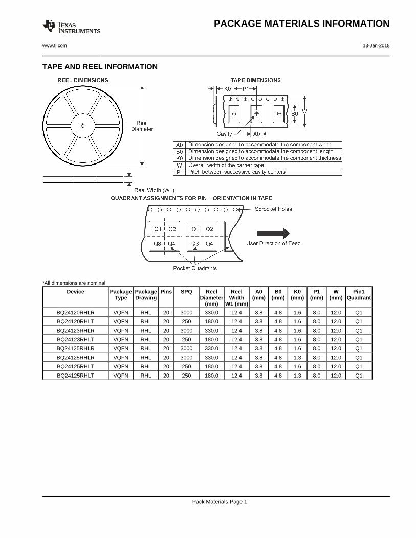
TAPE AND REEL INFORMATION
*All dimensions are nominal
Device PackageType
PackageDrawing
Pins SPQ ReelDiameter
(mm)
ReelWidth
W1 (mm)
A0(mm)
B0(mm)
K0(mm)
P1(mm)
W(mm)
Pin1Quadrant
BQ24120RHLR VQFN RHL 20 3000 330.0 12.4 3.8 4.8 1.6 8.0 12.0 Q1
BQ24120RHLT VQFN RHL 20 250 180.0 12.4 3.8 4.8 1.6 8.0 12.0 Q1
BQ24123RHLR VQFN RHL 20 3000 330.0 12.4 3.8 4.8 1.6 8.0 12.0 Q1
BQ24123RHLT VQFN RHL 20 250 180.0 12.4 3.8 4.8 1.6 8.0 12.0 Q1
BQ24125RHLR VQFN RHL 20 3000 330.0 12.4 3.8 4.8 1.6 8.0 12.0 Q1
BQ24125RHLR VQFN RHL 20 3000 330.0 12.4 3.8 4.8 1.3 8.0 12.0 Q1
BQ24125RHLT VQFN RHL 20 250 180.0 12.4 3.8 4.8 1.6 8.0 12.0 Q1
BQ24125RHLT VQFN RHL 20 250 180.0 12.4 3.8 4.8 1.3 8.0 12.0 Q1
PACKAGE MATERIALS INFORMATION
www.ti.com 13-Jan-2018
Pack Materials-Page 1

*All dimensions are nominal
Device Package Type Package Drawing Pins SPQ Length (mm) Width (mm) Height (mm)
BQ24120RHLR VQFN RHL 20 3000 367.0 367.0 35.0
BQ24120RHLT VQFN RHL 20 250 210.0 185.0 35.0
BQ24123RHLR VQFN RHL 20 3000 367.0 367.0 35.0
BQ24123RHLT VQFN RHL 20 250 210.0 185.0 35.0
BQ24125RHLR VQFN RHL 20 3000 367.0 367.0 35.0
BQ24125RHLR VQFN RHL 20 3000 370.0 355.0 55.0
BQ24125RHLT VQFN RHL 20 250 210.0 185.0 35.0
BQ24125RHLT VQFN RHL 20 250 195.0 200.0 45.0
PACKAGE MATERIALS INFORMATION
www.ti.com 13-Jan-2018
Pack Materials-Page 2


NOTES:
1. All linear dimensions are in millimeters. Any dimensions in parenthesis are for reference only. Dimensioning and tolerancingper ASME Y14.5M.
2. This drawing is subject to change without notice.3. The package thermal pad must be soldered to the printed circuit board for thermal and mechanical performance.
PACKAGE OUTLINE
4219071 / A 05/2017
www.ti.com
VQFN - 1 mm max height
PLASTIC QUAD FLATPACK- NO LEAD
RHL0020A
A
0.08 C
0.1 C A B0.05 C
B
SYMM
SYMM
PIN 1 INDEX AREA
SEATING PLANE
C
1PIN 1 ID(OPTIONAL)
2.05±0.1
3.05±0.1
3.63.4
4.64.4
1 MAX
(0.2) TYP
2X (0.55)
2X3.5
14X 0.5
2
9
10 11
12
19
20
2X 1.5
4X (0.2)
20X 0.290.19
20X 0.50.3
21
AutoCAD SHX Text
AutoCAD SHX Text
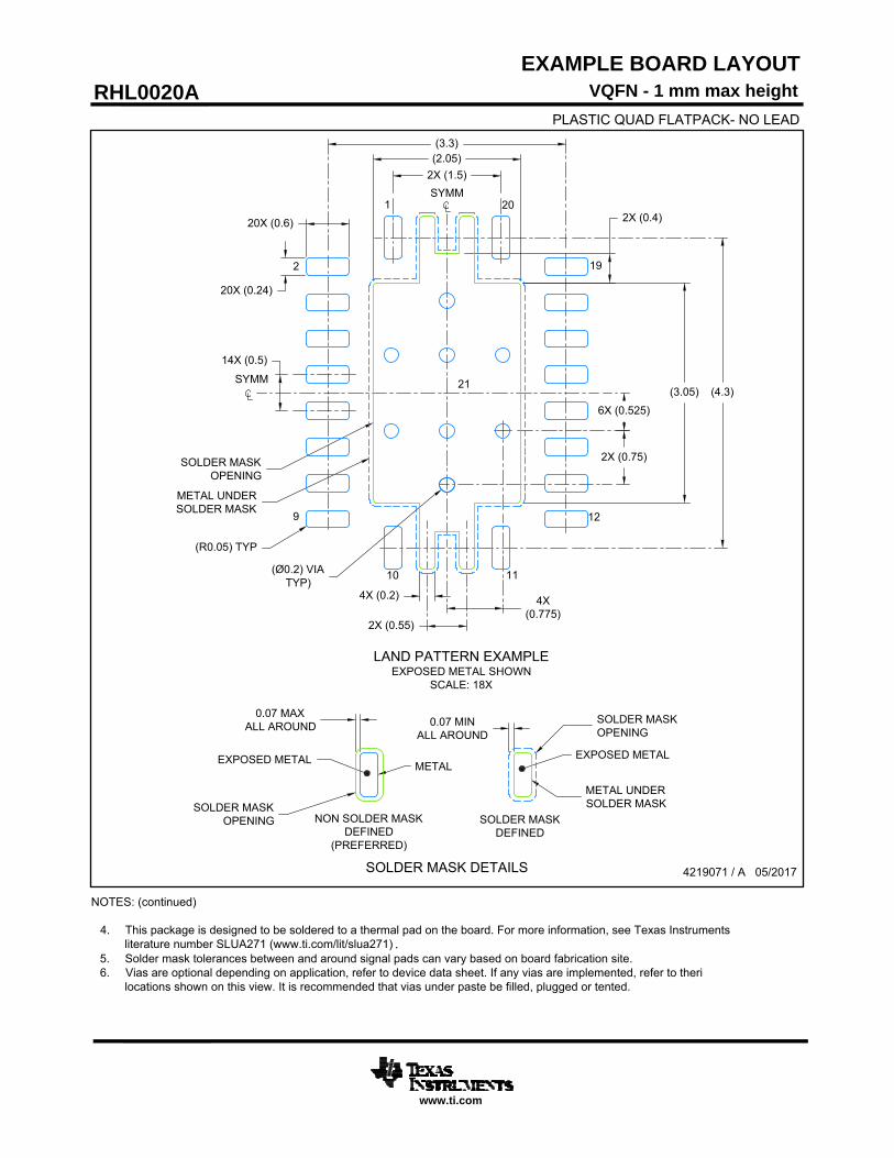
NOTES: (continued)
4. This package is designed to be soldered to a thermal pad on the board. For more information, see Texas Instrumentsliterature number SLUA271 (www.ti.com/lit/slua271) .
5. Solder mask tolerances between and around signal pads can vary based on board fabrication site.6. Vias are optional depending on application, refer to device data sheet. If any vias are implemented, refer to theri
locations shown on this view. It is recommended that vias under paste be filled, plugged or tented.
EXAMPLE BOARD LAYOUT
4219071 / A 05/2017
www.ti.com
VQFN - 1 mm max height
RHL0020A
PLASTIC QUAD FLATPACK- NO LEAD
SYMM
SYMM
LAND PATTERN EXAMPLEEXPOSED METAL SHOWN
SCALE: 18X
2X (1.5)
6X (0.525)
4X(0.775)
(4.3)
(3.3)
20X (0.6)
20X (0.24)
14X (0.5)
(3.05)
(2.05)
(R0.05) TYP
(Ø0.2) VIATYP)
1
2
9
10 11
12
19
20
0.07 MAXALL AROUND 0.07 MIN
ALL AROUND
SOLDER MASK DETAILS
NON SOLDER MASKDEFINED
(PREFERRED)
SOLDER MASKDEFINED
METAL
SOLDER MASKOPENING
SOLDER MASKOPENING
METAL UNDERSOLDER MASK
21
2X (0.75)
2X (0.4)
SOLDER MASKOPENING
METAL UNDERSOLDER MASK
4X (0.2)
2X (0.55)
EXPOSED METAL EXPOSED METAL
AutoCAD SHX Text
AutoCAD SHX Text

NOTES: (continued)
7. Laser cutting apertures with trapezoidal walls and rounded corners may offer better paste release. IPC-7525 may have alternatedesign recommendations..
EXAMPLE STENCIL DESIGN
4219071 / A 05/2017
www.ti.com
VQFN - 1 mm max height
RHL0020A
PLASTIC QUAD FLATPACK- NO LEAD
SYMM
SYMM
SOLDER PASTE EXAMPLEBASED ON 0.1mm THICK STENCIL
EXPOSED PAD75% PRINTED COVERAGE BY AREA
SCALE: 20X
(4.3)
2X (1.5)
(3.3)
(1.05)TYP
6X (0.92)
6X(0.85)
14X (0.5)
20X (0.24)
20X (0.6)
(0.56)TYP
METALTYP
21
4X (0.2)
2X (0.25)
(0.55)TYP
SOLDER MASK EDGETYP
2X(0.775)
1
2
9
10 11
12
19
20
(R0.05) TYP
AutoCAD SHX Text
AutoCAD SHX Text

IMPORTANT NOTICE
Texas Instruments Incorporated (TI) reserves the right to make corrections, enhancements, improvements and other changes to itssemiconductor products and services per JESD46, latest issue, and to discontinue any product or service per JESD48, latest issue. Buyersshould obtain the latest relevant information before placing orders and should verify that such information is current and complete.TI’s published terms of sale for semiconductor products (http://www.ti.com/sc/docs/stdterms.htm) apply to the sale of packaged integratedcircuit products that TI has qualified and released to market. Additional terms may apply to the use or sale of other types of TI products andservices.Reproduction of significant portions of TI information in TI data sheets is permissible only if reproduction is without alteration and isaccompanied by all associated warranties, conditions, limitations, and notices. TI is not responsible or liable for such reproduceddocumentation. Information of third parties may be subject to additional restrictions. Resale of TI products or services with statementsdifferent from or beyond the parameters stated by TI for that product or service voids all express and any implied warranties for theassociated TI product or service and is an unfair and deceptive business practice. TI is not responsible or liable for any such statements.Buyers and others who are developing systems that incorporate TI products (collectively, “Designers”) understand and agree that Designersremain responsible for using their independent analysis, evaluation and judgment in designing their applications and that Designers havefull and exclusive responsibility to assure the safety of Designers' applications and compliance of their applications (and of all TI productsused in or for Designers’ applications) with all applicable regulations, laws and other applicable requirements. Designer represents that, withrespect to their applications, Designer has all the necessary expertise to create and implement safeguards that (1) anticipate dangerousconsequences of failures, (2) monitor failures and their consequences, and (3) lessen the likelihood of failures that might cause harm andtake appropriate actions. Designer agrees that prior to using or distributing any applications that include TI products, Designer willthoroughly test such applications and the functionality of such TI products as used in such applications.TI’s provision of technical, application or other design advice, quality characterization, reliability data or other services or information,including, but not limited to, reference designs and materials relating to evaluation modules, (collectively, “TI Resources”) are intended toassist designers who are developing applications that incorporate TI products; by downloading, accessing or using TI Resources in anyway, Designer (individually or, if Designer is acting on behalf of a company, Designer’s company) agrees to use any particular TI Resourcesolely for this purpose and subject to the terms of this Notice.TI’s provision of TI Resources does not expand or otherwise alter TI’s applicable published warranties or warranty disclaimers for TIproducts, and no additional obligations or liabilities arise from TI providing such TI Resources. TI reserves the right to make corrections,enhancements, improvements and other changes to its TI Resources. TI has not conducted any testing other than that specificallydescribed in the published documentation for a particular TI Resource.Designer is authorized to use, copy and modify any individual TI Resource only in connection with the development of applications thatinclude the TI product(s) identified in such TI Resource. NO OTHER LICENSE, EXPRESS OR IMPLIED, BY ESTOPPEL OR OTHERWISETO ANY OTHER TI INTELLECTUAL PROPERTY RIGHT, AND NO LICENSE TO ANY TECHNOLOGY OR INTELLECTUAL PROPERTYRIGHT OF TI OR ANY THIRD PARTY IS GRANTED HEREIN, including but not limited to any patent right, copyright, mask work right, orother intellectual property right relating to any combination, machine, or process in which TI products or services are used. Informationregarding or referencing third-party products or services does not constitute a license to use such products or services, or a warranty orendorsement thereof. Use of TI Resources may require a license from a third party under the patents or other intellectual property of thethird party, or a license from TI under the patents or other intellectual property of TI.TI RESOURCES ARE PROVIDED “AS IS” AND WITH ALL FAULTS. TI DISCLAIMS ALL OTHER WARRANTIES ORREPRESENTATIONS, EXPRESS OR IMPLIED, REGARDING RESOURCES OR USE THEREOF, INCLUDING BUT NOT LIMITED TOACCURACY OR COMPLETENESS, TITLE, ANY EPIDEMIC FAILURE WARRANTY AND ANY IMPLIED WARRANTIES OFMERCHANTABILITY, FITNESS FOR A PARTICULAR PURPOSE, AND NON-INFRINGEMENT OF ANY THIRD PARTY INTELLECTUALPROPERTY RIGHTS. TI SHALL NOT BE LIABLE FOR AND SHALL NOT DEFEND OR INDEMNIFY DESIGNER AGAINST ANY CLAIM,INCLUDING BUT NOT LIMITED TO ANY INFRINGEMENT CLAIM THAT RELATES TO OR IS BASED ON ANY COMBINATION OFPRODUCTS EVEN IF DESCRIBED IN TI RESOURCES OR OTHERWISE. IN NO EVENT SHALL TI BE LIABLE FOR ANY ACTUAL,DIRECT, SPECIAL, COLLATERAL, INDIRECT, PUNITIVE, INCIDENTAL, CONSEQUENTIAL OR EXEMPLARY DAMAGES INCONNECTION WITH OR ARISING OUT OF TI RESOURCES OR USE THEREOF, AND REGARDLESS OF WHETHER TI HAS BEENADVISED OF THE POSSIBILITY OF SUCH DAMAGES.Unless TI has explicitly designated an individual product as meeting the requirements of a particular industry standard (e.g., ISO/TS 16949and ISO 26262), TI is not responsible for any failure to meet such industry standard requirements.Where TI specifically promotes products as facilitating functional safety or as compliant with industry functional safety standards, suchproducts are intended to help enable customers to design and create their own applications that meet applicable functional safety standardsand requirements. Using products in an application does not by itself establish any safety features in the application. Designers mustensure compliance with safety-related requirements and standards applicable to their applications. Designer may not use any TI products inlife-critical medical equipment unless authorized officers of the parties have executed a special contract specifically governing such use.Life-critical medical equipment is medical equipment where failure of such equipment would cause serious bodily injury or death (e.g., lifesupport, pacemakers, defibrillators, heart pumps, neurostimulators, and implantables). Such equipment includes, without limitation, allmedical devices identified by the U.S. Food and Drug Administration as Class III devices and equivalent classifications outside the U.S.TI may expressly designate certain products as completing a particular qualification (e.g., Q100, Military Grade, or Enhanced Product).Designers agree that it has the necessary expertise to select the product with the appropriate qualification designation for their applicationsand that proper product selection is at Designers’ own risk. Designers are solely responsible for compliance with all legal and regulatoryrequirements in connection with such selection.Designer will fully indemnify TI and its representatives against any damages, costs, losses, and/or liabilities arising out of Designer’s non-compliance with the terms and provisions of this Notice.
Mailing Address: Texas Instruments, Post Office Box 655303, Dallas, Texas 75265Copyright © 2018, Texas Instruments Incorporated