


Integrated 5-A 40-V Wide Input Range … · powerpad 16 ss en vin sw freq nc pgnd pgnd sw sw nc...
44
50 55 60 65 70 75 80 85 90 95 100 0 0.4 0.8 1.2 1.6 2 2.4 Output Current (A) Efficiency (%) V IN = 15 V V IN = 12 V V IN = 5 V V OUT = 24 V f SW = 600 kHz G031 TPS55340 VIN EN SW SW SW FREQ SS COMP SYNC FB PGND PGND PGND VIN VOUT RSL RSH L D CI CO RFREQ CSS RC CC AGND Product Folder Sample & Buy Technical Documents Tools & Software Support & Community An IMPORTANT NOTICE at the end of this data sheet addresses availability, warranty, changes, use in safety-critical applications, intellectual property matters and other important disclaimers. PRODUCTION DATA. TPS55340 SLVSBD4C – MAY 2012 – REVISED JANUARY 2015 TPS55340 Integrated 5-A Wide Input Range Boost/SEPIC/Flyback DC-DC Regulator 1 1 Features 1• Internal 5-A, 40-V Low-Side MOSFET Switch • 2.9-V to 32-V Input Voltage Range • ±0.7% Reference Voltage • 0.5-mA Operating Quiescent Current • 2.7-μA Shutdown Supply Current • Fixed Frequency Current Mode PWM Control • Frequency Adjustable From 100 kHz to 1.2 MHz • Synchronization Capability to External Clock • Adjustable Soft-Start Time • Pulse Skipping for Higher Efficiency at Light Loads • Cycle-by-Cycle Current Limit, Thermal Shutdown, and UVLO Protection • QFN-16 (3-mm × 3-mm) and HTSSOP-14 Packages With PowerPAD™ • Wide –40°C to 150°C Operating T J Range • Create a Custom Design Using the TPS55340 with the WEBENCH Power Designer 2 Applications • 3.3-V, 5-V, 12-V, 24-V Power Conversion • Boost, SEPIC, and Flyback Topologies • Thunderbolt Port, USB Type-C Power Delivery, Power Docking for Tablets and Portable PCs • Industrial Power Systems • ADSL Modems 3 Description The TPS55340 is a monolithic, nonsynchronous, switching regulator with integrated 5-A, 40-V power switch. The device can be configured in several standard switching-regulator topologies, including boost, SEPIC, and isolated flyback. The device has a wide input voltage range to support applications with input voltage from multicell batteries or regulated 3.3-V, 5-V, 12-V, and 24-V power rails. The TPS55340 regulates the output voltage with current mode PWM (pulse width modulation) control, and has an internal oscillator. The switching frequency of PWM is set by either an external resistor or by synchronizing to an external clock signal. The user can program the switching frequency from 100 kHz to 1.2 MHz. The device features a programmable soft-start function to limit inrush current during start-up and has other built-in protection features including cycle-by- cycle overcurrent limit and thermal shutdown. The TPS55340 is available in a small 3-mm × 3-mm 16-pin QFN as well as 14-pin HTSSOP packages with PowerPAD for enhanced thermal performance. The 5-A, 40-V TPS55340 boost converter in the HTSSOP-14 package is pin-to-pin compatible with the 3-A, 40-V TPS61175 and it extends the maximum input voltage from 18 V to 32 V. Device Information (1) PART NUMBER PACKAGE BODY SIZE (NOM) TPS55340 HTSSOP (14) 5.00 mm × 4.40 mm WQFN (16) 3.00 mm × 3.00 mm (1) For all available packages, see the orderable addendum at the end of the data sheet. Typical Application (Boost) Efficiency vs Output Current
Transcript of Integrated 5-A 40-V Wide Input Range … · powerpad 16 ss en vin sw freq nc pgnd pgnd sw sw nc...
50
55
60
65
70
75
80
85
90
95
100
0 0.4 0.8 1.2 1.6 2 2.4Output Current (A)
Effi
cien
cy (
%)
VIN = 15 VVIN = 12 VVIN = 5 V
VOUT = 24 VfSW = 600 kHz
G031
TPS55340
VIN
EN
SW
SW
SWFREQ
SS
COMP
SYNC
FB
PGND
PGND
PGND
VIN VOUT
RSL
RSH
L D
CI CO
RFREQ
CSS
RC
CC
AGND
Product
Folder
Sample &Buy
Technical
Documents
Tools &
Software
Support &Community
An IMPORTANT NOTICE at the end of this data sheet addresses availability, warranty, changes, use in safety-critical applications,intellectual property matters and other important disclaimers. PRODUCTION DATA.
TPS55340SLVSBD4C –MAY 2012–REVISED JANUARY 2015
TPS55340 Integrated 5-A Wide Input Range Boost/SEPIC/Flyback DC-DC Regulator
1
1 Features1• Internal 5-A, 40-V Low-Side MOSFET Switch• 2.9-V to 32-V Input Voltage Range• ±0.7% Reference Voltage• 0.5-mA Operating Quiescent Current• 2.7-µA Shutdown Supply Current• Fixed Frequency Current Mode PWM Control• Frequency Adjustable From 100 kHz to 1.2 MHz• Synchronization Capability to External Clock• Adjustable Soft-Start Time• Pulse Skipping for Higher Efficiency at Light
Loads• Cycle-by-Cycle Current Limit, Thermal Shutdown,
and UVLO Protection• QFN-16 (3-mm × 3-mm) and HTSSOP-14
Packages With PowerPAD™• Wide –40°C to 150°C Operating TJ Range• Create a Custom Design Using the TPS55340
with the WEBENCH Power Designer
2 Applications• 3.3-V, 5-V, 12-V, 24-V Power Conversion• Boost, SEPIC, and Flyback Topologies• Thunderbolt Port, USB Type-C Power Delivery,
Power Docking for Tablets and Portable PCs• Industrial Power Systems• ADSL Modems
3 DescriptionThe TPS55340 is a monolithic, nonsynchronous,switching regulator with integrated 5-A, 40-V powerswitch. The device can be configured in severalstandard switching-regulator topologies, includingboost, SEPIC, and isolated flyback. The device has awide input voltage range to support applications withinput voltage from multicell batteries or regulated3.3-V, 5-V, 12-V, and 24-V power rails.
The TPS55340 regulates the output voltage withcurrent mode PWM (pulse width modulation) control,and has an internal oscillator. The switchingfrequency of PWM is set by either an external resistoror by synchronizing to an external clock signal. Theuser can program the switching frequency from100 kHz to 1.2 MHz.
The device features a programmable soft-startfunction to limit inrush current during start-up and hasother built-in protection features including cycle-by-cycle overcurrent limit and thermal shutdown.
The TPS55340 is available in a small 3-mm × 3-mm16-pin QFN as well as 14-pin HTSSOP packageswith PowerPAD for enhanced thermal performance.
The 5-A, 40-V TPS55340 boost converter in theHTSSOP-14 package is pin-to-pin compatible withthe 3-A, 40-V TPS61175 and it extends the maximuminput voltage from 18 V to 32 V.
Device Information(1)
PART NUMBER PACKAGE BODY SIZE (NOM)
TPS55340HTSSOP (14) 5.00 mm × 4.40 mmWQFN (16) 3.00 mm × 3.00 mm
(1) For all available packages, see the orderable addendum atthe end of the data sheet.
Typical Application (Boost) Efficiency vs Output Current
2
TPS55340SLVSBD4C –MAY 2012–REVISED JANUARY 2015 www.ti.com
Product Folder Links: TPS55340
Submit Documentation Feedback Copyright © 2012–2015, Texas Instruments Incorporated
Table of Contents1 Features .................................................................. 12 Applications ........................................................... 13 Description ............................................................. 14 Revision History..................................................... 25 Pin Configuration and Functions ......................... 36 Specifications......................................................... 4
6.1 Absolute Maximum Ratings ...................................... 46.2 ESD Ratings.............................................................. 46.3 Recommended Operating Conditions....................... 46.4 Thermal Information .................................................. 46.5 Electrical Characteristics........................................... 56.6 Typical Characteristics .............................................. 6
7 Detailed Description .............................................. 97.1 Overview ................................................................... 97.2 Functional Block Diagram ......................................... 97.3 Feature Description................................................... 9
7.4 Device Functional Modes........................................ 128 Application and Implementation ........................ 13
8.1 Application Information............................................ 138.2 Typical Applications ................................................ 13
9 Power Supply Recommendations ...................... 2710 Layout................................................................... 27
10.1 Layout Guidelines ................................................. 2710.2 Layout Example .................................................... 2710.3 Thermal Considerations ........................................ 28
11 Device and Documentation Support ................. 2911.1 Custom Design with WEBENCH Tools................. 2911.2 Receiving Notification of Documentation Updates 2911.3 Trademarks ........................................................... 2911.4 Electrostatic Discharge Caution............................ 2911.5 Glossary ................................................................ 29
12 Mechanical, Packaging, and OrderableInformation ........................................................... 29
4 Revision History
Changes from Revision B (October 2012) to Revision C Page
• Added Pin Configuration and Functions section, ESD Ratings table, Feature Description section, Device FunctionalModes, Application and Implementation section, Power Supply Recommendations section, Layout section, Deviceand Documentation Support section, and Mechanical, Packaging, and Orderable Information section .............................. 1
Changes from Revision A (October 2012) to Revision B Page
• Corrected the pin numbers to the QFN-16 Package drawing ................................................................................................ 3
Changes from Original (May 2012) to Revision A Page
• Added PWP package ............................................................................................................................................................. 1• Added HTSSOP-14 package to FEATURES ......................................................................................................................... 1• Added 14-pin HTSSOP package to DESCRIPTION .............................................................................................................. 1• Added paragraph to end of DESCRIPTION ........................................................................................................................... 1• Added PWP package to PIN ASSIGNMENTS ....................................................................................................................... 3• Added PWP package to PIN FUNCTIONS ............................................................................................................................ 3• Added HTSSOP package to THERMAL INFORMATION ...................................................................................................... 4
PowerPAD
16
SS
EN
VIN
SW
FREQ
NC
PGND
PGND
SW
SW
NC
PG
ND
SY
NC
AG
ND
CO
MP
FB
15 14 13
5 6 7 8
1
2
3
4
12
11
10
9
1
7
6
5
4
3
2
14
8
9
10
11
12
13
SW
SW
VIN
EN
SS
SYNC
AGND
PGND
PGND
NC
FREQ
FB
COMP
PGND
PowerPAD
3
TPS55340www.ti.com SLVSBD4C –MAY 2012–REVISED JANUARY 2015
Product Folder Links: TPS55340
Submit Documentation FeedbackCopyright © 2012–2015, Texas Instruments Incorporated
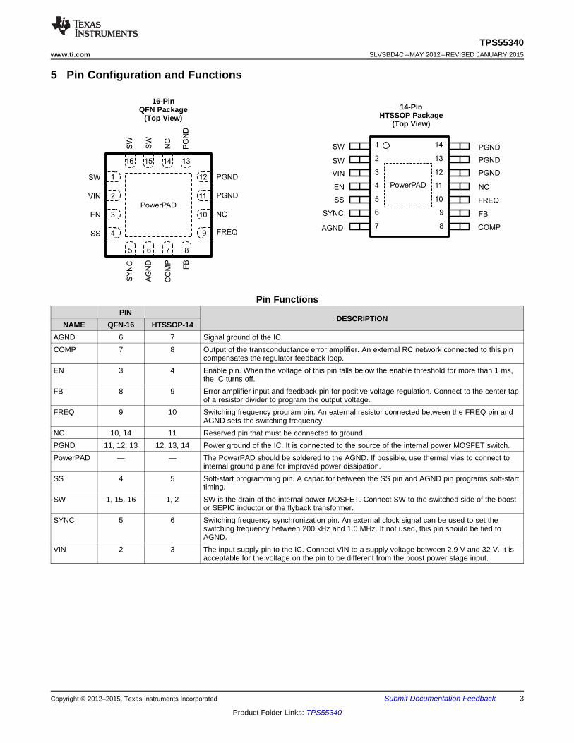
5 Pin Configuration and Functions
16-PinQFN Package
(Top View)14-Pin
HTSSOP Package(Top View)
Pin FunctionsPIN
DESCRIPTIONNAME QFN-16 HTSSOP-14
AGND 6 7 Signal ground of the IC.COMP 7 8 Output of the transconductance error amplifier. An external RC network connected to this pin
compensates the regulator feedback loop.EN 3 4 Enable pin. When the voltage of this pin falls below the enable threshold for more than 1 ms,
the IC turns off.FB 8 9 Error amplifier input and feedback pin for positive voltage regulation. Connect to the center tap
of a resistor divider to program the output voltage.FREQ 9 10 Switching frequency program pin. An external resistor connected between the FREQ pin and
AGND sets the switching frequency.NC 10, 14 11 Reserved pin that must be connected to ground.PGND 11, 12, 13 12, 13, 14 Power ground of the IC. It is connected to the source of the internal power MOSFET switch.PowerPAD — — The PowerPAD should be soldered to the AGND. If possible, use thermal vias to connect to
internal ground plane for improved power dissipation.SS 4 5 Soft-start programming pin. A capacitor between the SS pin and AGND pin programs soft-start
timing.SW 1, 15, 16 1, 2 SW is the drain of the internal power MOSFET. Connect SW to the switched side of the boost
or SEPIC inductor or the flyback transformer.SYNC 5 6 Switching frequency synchronization pin. An external clock signal can be used to set the
switching frequency between 200 kHz and 1.0 MHz. If not used, this pin should be tied toAGND.
VIN 2 3 The input supply pin to the IC. Connect VIN to a supply voltage between 2.9 V and 32 V. It isacceptable for the voltage on the pin to be different from the boost power stage input.
4
TPS55340SLVSBD4C –MAY 2012–REVISED JANUARY 2015 www.ti.com
Product Folder Links: TPS55340
Submit Documentation Feedback Copyright © 2012–2015, Texas Instruments Incorporated
(1) Stresses beyond those listed under Absolute Maximum Ratings may cause permanent damage to the device. These are stress ratingsonly and functional operation of the device at these or any other conditions beyond those indicated under Recommended OperatingConditions is not implied. Exposure to absolute-maximum-rated conditions for extended periods may affect device reliability.
(2) All voltage values are with respect to network ground terminal
6 Specifications
6.1 Absolute Maximum Ratingsover operating temperature range (unless otherwise noted) (1)
MIN MAX UNITSupply voltages on pin VIN (2) –0.3 34 VVoltage on pin EN (2) –0.3 34 VVoltage on pins FB, FREQ, and COMP (2) –0.3 3 VVoltage on pin SS (2) –0.3 5 VVoltage on pin SYNC (2) –0.3 7 VVoltage on pin SW (2) –0.3 40 VOperating junction temperature –40 150 °CStorage temperature, Tstg –65 150 °C
(1) JEDEC document JEP155 states that 500-V HBM allows safe manufacturing with a standard ESD control process.(2) JEDEC document JEP157 states that 250-V CDM allows safe manufacturing with a standard ESD control process.
6.2 ESD RatingsVALUE UNIT
V(ESD) Electrostatic dischargeHuman body model (HBM), per ANSI/ESDA/JEDEC JS-001, all pins (1) ±2000
VCharged device model (CDM), per JEDEC specification JESD22-C101, allpins (2)
±500
6.3 Recommended Operating ConditionsMIN NOM MAX UNIT
VIN Input voltage range 2.9 32 VVOUT Output voltage range VIN 38 VVEN EN voltage range 0 32 VVSYN External switching frequency logic input range 0 5 VTA Operating free-air temperature –40 125 °CTJ Operating junction temperature –40 150 °C
(1) For more information about traditional and new thermal metrics, see the Semiconductor and IC Package Thermal Metrics applicationreport (SPRA953).
6.4 Thermal Information
THERMAL METRIC (1)TPS55340
UNITQFN(16 PINS)
HTSSOP(14 PINS)
RθJA Junction-to-ambient thermal resistance 43.3 43.2
°C/W
RθJC(top) Junction-to-case (top) thermal resistance 38.7 33.3RθJB Junction-to-board thermal resistance 14.5 28.3ψJT Junction-to-top characterization parameter 0.4 1.3ψJB Junction-to-board characterization parameter 14.5 28.1RθJC(bot) Junction-to-case (bottom) thermal resistance 3.5 3.9
5
TPS55340www.ti.com SLVSBD4C –MAY 2012–REVISED JANUARY 2015
Product Folder Links: TPS55340
Submit Documentation FeedbackCopyright © 2012–2015, Texas Instruments Incorporated
6.5 Electrical CharacteristicsVIN = 5 V, TJ = –40°C to 150°C, unless otherwise noted. Typical values are at TA = 25°C.
PARAMETER TEST CONDITIONS MIN TYP MAX UNITSUPPLY CURRENTVIN Input voltage range 2.9 32 VIQ Operating quiescent current into VIN Device nonswitching, VFB = 2 V 0.5 mAISD Shutdown current EN = GND 2.7 10 µAVUVLO Undervoltage lockout threshold VIN falling 2.5 2.7 VVhys Undervoltage lockout hysteresis 120 140 160 mVENABLE AND REFERENCE CONTROLVEN EN threshold voltage EN rising input 0.9 1.08 1.30 VVEN EN threshold voltage EN falling input 0.74 0.92 1.125 VVENh EN threshold hysteresis 0.16 VREN EN pulldown resistor 400 950 1600 kΩToff Shutdown delay, SS discharge EN high to low 1.0 msVSYNh SYN logic high voltage 1.2 VVSYNl SYN logic low voltage 0.4 VVOLTAGE AND CURRENT CONTROL
VREF Voltage feedback regulation voltage1.204 1.229 1.254
VTA = 25°C 1.220 1.229 1.238
IFB Voltage feedback input bias current TA = 25°C 1.6 20 nAIsink COMP pin sink current VFB = VREF + 200 mV, VCOMP = 1 V 42 µAIsource COMP pin source current VFB = VREF – 200 mV, VCOMP = 1 V 42 µA
VCCLP COMP pin clamp voltageHigh Clamp, VFB = 1 V 3.1
VLow Clamp, VFB = 1.5 V 0.75
VCTH COMP pin threshold Duty cycle = 0% 1.04 VGea Error amplifier transconductance 240 360 440 µSRea Error amplifier output resistance 10 MΩ
fea Error amplifier crossover frequency 500 kHzFREQUENCY
fSW FrequencyRFREQ = 480 kΩ 75 94 130
kHzRFREQ = 80 kΩ 460 577 740RFREQ = 40 kΩ 920 1140 1480
Dmax Maximum duty cycle VFB = 1.0 V, RFREQ = 80 kΩ 89% 96%VFREQ FREQ pin voltage 1.25 VTmin_on Minimum on pulse width RFREQ = 80 kΩ 77 nsPOWER SWITCH
RDS(ON) N-channel MOSFET on-resistanceVIN = 5 V 60 110
mΩVIN = 3 V 70 120
ILN_NFET N-channel leakage current VDS = 25 V, TA = 25°C 2.1 µAOCP and SSILIM N-channel MOSFET current limit D = Dmax 5.25 6.6 7.75 AISS Soft-start bias current VSS = 0 V 6 µATHERMAL SHUTDOWNTshutdown Thermal shutdown threshold 165 °C
ThysteresisThermal shutdown thresholdhysteresis 15 °C
0
200
400
600
800
1000
1200
1400
1600
30 100 500Resistance (kΩ)
Fre
quen
cy (
kHz)
G005
0
200
400
600
800
1000
1200
1400
−50 −25 0 25 50 75 100 125 150Temperature (°C)
Fre
quen
cy (
kHz)
RFREQ = 40 kΩRFREQ = 80 kΩRFREQ = 480 kΩ
G006
1.22
1.222
1.224
1.226
1.228
1.23
−50 −25 0 25 50 75 100 125 150Temperature (°C)
Vol
tage
Ref
eren
ce (
V)
G003
0
20
40
60
80
100
120
−50 −25 0 25 50 75 100 125 150
VIN = 3 V
VIN = 5 VVIN = 12 V
Temperature (°C)
Res
ista
nce
(mΩ
)
G004
300
320
340
360
380
400
−50 −25 0 25 50 75 100 125 150Temperature (°C)
Tra
nsco
nduc
tanc
e (µ
A/V
)
G001
1
2
3
4
5
6
7
8
−50 −25 0 25 50 75 100 125 150Temperature (°C)
Cur
rent
Lim
it T
hres
hold
(A
)
G002
6
TPS55340SLVSBD4C –MAY 2012–REVISED JANUARY 2015 www.ti.com
Product Folder Links: TPS55340
Submit Documentation Feedback Copyright © 2012–2015, Texas Instruments Incorporated
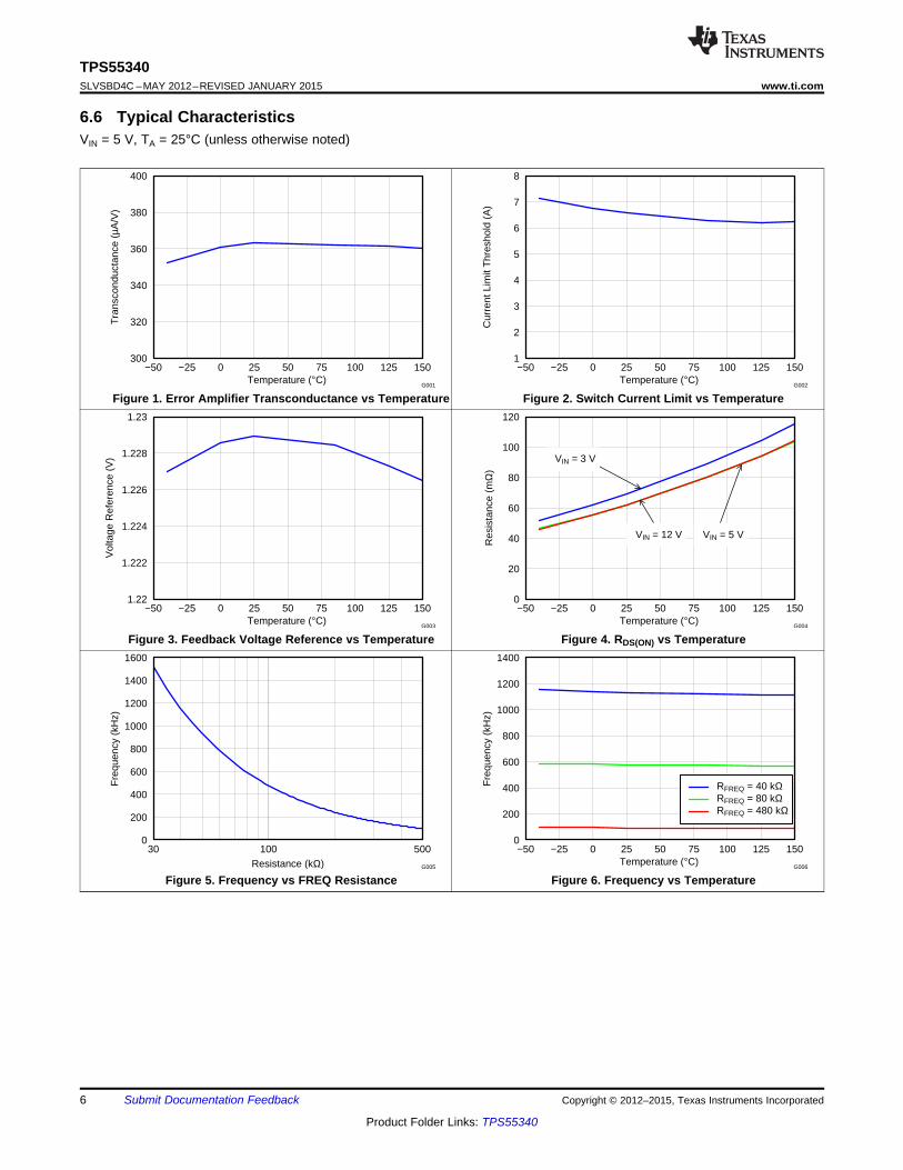
6.6 Typical CharacteristicsVIN = 5 V, TA = 25°C (unless otherwise noted)
Figure 1. Error Amplifier Transconductance vs Temperature Figure 2. Switch Current Limit vs Temperature
Figure 3. Feedback Voltage Reference vs Temperature Figure 4. RDS(ON) vs Temperature
Figure 5. Frequency vs FREQ Resistance Figure 6. Frequency vs Temperature
0.7
0.8
0.9
1
1.1
1.2
1.3
−50 −25 0 25 50 75 100 125 150Temperature (°C)
Ena
ble
Vol
tage
(V
)
EN Voltage RisingEN Voltage Falling
G010
94
95
96
97
98
99
100
−50 −25 0 25 50 75 100 125 150Temperature (°C)
Max
imum
Dut
y C
ycle
(%
)
RFREQ = 80 kΩ
G011
2.5
2.54
2.58
2.62
2.66
2.7
−50 −25 0 25 50 75 100 125 150Temperature (°C)
Inpu
t Vol
tage
(V
)
UVLO StartUVLO Stop
G009
0.5
1
1.5
2
2.5
3
3.5
−50 −25 0 25 50 75 100 125 150Temperature (°C)
CO
MP
Vol
tage
(V
)
COMP Pin Clamp HighCOMP Pin Clamp Low
G008
0
100
200
300
400
500
600
700
−50 −25 0 25 50 75 100 125 150Temperature (°C)
Fre
quen
cy (
kHz)
Non-FoldbackFoldback
RFREQ = 80 kΩ
G007 Voltage on the VIN Pin (V)
Fre
quen
cy (
kHz)
0 5 10 15 20 25 30 35 400
50
100
150
200
250
300
350
400
D006
7
TPS55340www.ti.com SLVSBD4C –MAY 2012–REVISED JANUARY 2015
Product Folder Links: TPS55340
Submit Documentation FeedbackCopyright © 2012–2015, Texas Instruments Incorporated
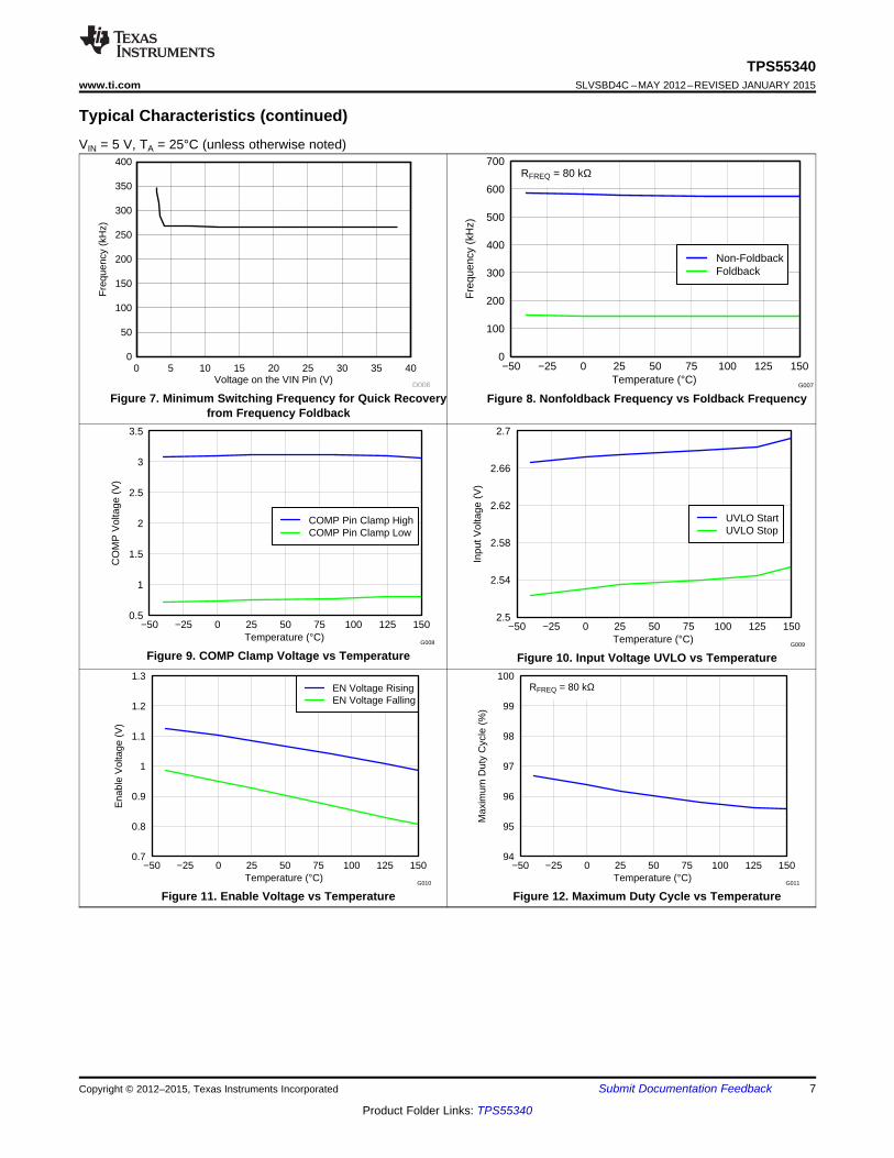
Typical Characteristics (continued)VIN = 5 V, TA = 25°C (unless otherwise noted)
Figure 7. Minimum Switching Frequency for Quick Recoveryfrom Frequency Foldback
Figure 8. Nonfoldback Frequency vs Foldback Frequency
Figure 9. COMP Clamp Voltage vs Temperature Figure 10. Input Voltage UVLO vs Temperature
Figure 11. Enable Voltage vs Temperature Figure 12. Maximum Duty Cycle vs Temperature
0.3
0.6
0.9
1.2
1.5
1.8
2.1
−50 −25 0 25 50 75 100 125 150Temperature (°C)
Sup
ply
Cur
rent
(m
A)
SwitchingNon-Switching
G014
70
75
80
85
90
95
100
−50 −25 0 25 50 75 100 125 150Temperature (°C)
Min
imum
On
Tim
e (n
s)
RFREQ = 80 kΩ
G012
1
2
3
4
5
6
7
8
−50 −25 0 25 50 75 100 125 150Temperature (°C)
Shu
tdow
n C
urre
nt (
µA)
G013
8
TPS55340SLVSBD4C –MAY 2012–REVISED JANUARY 2015 www.ti.com
Product Folder Links: TPS55340
Submit Documentation Feedback Copyright © 2012–2015, Texas Instruments Incorporated
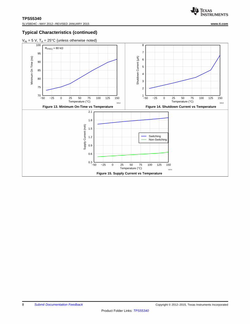
Typical Characteristics (continued)VIN = 5 V, TA = 25°C (unless otherwise noted)
Figure 13. Minimum On-Time vs Temperature Figure 14. Shutdown Current vs Temperature
Figure 15. Supply Current vs Temperature
SW
Ramp
Generator
Lossless
Current Sense
EN
PGND
Error
Amp
VIN
PWM
Control
COMP
SS FREQ SYNC
FB
AGND
1.229V
Reference
S
Oscillator
Gate
Driver
9
TPS55340www.ti.com SLVSBD4C –MAY 2012–REVISED JANUARY 2015
Product Folder Links: TPS55340
Submit Documentation FeedbackCopyright © 2012–2015, Texas Instruments Incorporated
7 Detailed Description
7.1 OverviewThe TPS55340 device is a monolithic, nonsynchronous, switching regulator with an integrated 5-A, 40-V powerswitch. The device can be configured in several standard switching-regulator topologies, including boost, SEPIC,and isolated flyback. The device has a wide input voltage range to support applications with input voltage frommulticell batteries or regulated 3.3-V, 5-V, 12-V, and 24-V power rails.
7.2 Functional Block Diagram
7.3 Feature Description
7.3.1 OperationIf designed as a boost converter, the TPS55340 device regulates the output with current-mode, pulse-width-modulation (PWM) control. The PWM control circuitry turns on the switch at the beginning of each oscillator clockcycle. The input voltage is applied across the inductor and stores the energy as inductor current ramps up.During this portion of the switching cycle, the load current is provided by the output capacitor. When the inductorcurrent reaches a threshold level set by the error amplifier output, the power switch turns off and the externalSchottky diode is forward biased to allow the inductor current to flow to the output. The inductor transfers storedenergy to replenish the output capacitor and supply the load current. This operation repeats every switchingcycle. The duty cycle of the converter is determined by the PWM control comparator which compares the erroramplifier output and the current signal. The oscillator frequency is programmed by the external resistor orsynchronized to an external clock signal.
10
TPS55340SLVSBD4C –MAY 2012–REVISED JANUARY 2015 www.ti.com
Product Folder Links: TPS55340
Submit Documentation Feedback Copyright © 2012–2015, Texas Instruments Incorporated
Feature Description (continued)A ramp signal from the oscillator is added to the inductor current ramp to provide slope compensation. Slopecompensation is required to avoid subharmonic oscillation that is intrinsic to peak-current mode control at dutycycles higher than 50%. If the inductor value is too small, the internal slope compensation may not be adequateto maintain stability.
The PWM control feedback loop regulates the FB pin to a reference voltage through a transconductance erroramplifier. The output of the error amplifier is connected to the COMP pin. An external RC compensation networkconnected to the COMP pin is chosen for feedback loop stability and optimum transient response.
7.3.2 Switching FrequencyThe switching frequency is set by a resistor (RFREQ) connected to the FREQ pin of the TPS55340. Therelationship between the timing resistance RFREQ and frequency is shown in the Figure 5. Do not leave this pinopen. A resistor must always be connected from the FREQ pin to ground for proper operation. The resistor valuerequired for a desired frequency can be calculated using Equation 1.
RFREQ(kΩ) = 57500 × ƒsw(kHz)–1.03 (1)
For the given resistor value, the corresponding frequency can be calculated by Equation 2.ƒsw(kHz) = 41600 × RFREQ(kΩ)–0.97 (2)
The TPS55340 switching frequency can be synchronized to an external clock signal that is applied to the SYNCpin. The required logic levels of the external clock are shown in Recommended Operating Conditions. Therecommended duty cycle of the clock is in the range of 10% to 90%. A resistor must be connected from theFREQ pin to ground when the converter is synchronized to the external clock and the external clock frequencymust be within ±20% of the corresponding frequency set by the resistor. For example, if the frequencyprogrammed by the FREQ pin resistor is 600 kHz, the external clock signal should be in the range of 480 kHz to720 kHz.
With a switching frequency below 280 kHz (typical) after the TPS55340 enters frequency foldback as describedin Overcurrent Protection and Frequency Foldback, if a load remains when the overcurrent condition is removed,then the output may not recover to the set value. For the output to return to the set value, the load must beremoved completely or the TPS55340 power cycled with the EN pin or VIN pin. Select a nominal switchingfrequency of 350 kHz for quicker recovery from frequency foldback.
7.3.3 Overcurrent Protection and Frequency FoldbackThe TPS55340 provides cycle-by-cycle overcurrent protection that turns off the power switch once the inductorcurrent reaches the overcurrent limit threshold. The PWM circuitry resets itself at the beginning of the next switchcycle. During an overcurrent event, the output voltage begins to drop as a function of the load on the output.When the FB voltage through the feedback resistors drops lower than 0.9 V, the switching frequency isautomatically reduced to 1/4 of the normal value. Figure 8 shows the nonfoldback frequency with an 80-kΩ timingresistor and the corresponding foldback frequency. The switching frequency does not return to normal until theovercurrent condition is removed and the FB voltage increases above 0.9 V. The frequency foldback feature isdisabled during soft-start.
7.3.3.1 Minimum On-Time and Pulse SkippingThe TPS55340 PWM control system has a minimum PWM pulse width of 77 ns (typical). This minimum on-timedetermines the minimum duty cycle of the PWM for any set switching frequency. When the voltage regulationloop of the TPS55340 requires a minimum on-time pulse width less than 77 ns, the IC enters pulse skippingmode. In this mode, the device will hold the power switch off for several switching cycles to prevent the outputvoltage from rising above the desired regulated voltage. This operation typically occurs in light load conditionswhen the PWM operates in discontinuous conduction mode. Pulse skipping increases the output ripple as shownin Figure 22.
7.3.4 Voltage Reference and Setting Output VoltageAn internal voltage reference provides a precise 1.229-V voltage reference at the error amplifier noninvertinginput. To set the output voltage, select the FB pin resistor RSH and RSL according to Equation 3.
( )
1He(s)
Se
s 1 (1 D) 0.52S
sn1
2fsw f
sw
=é ùæ ö
ê úç ÷´ + ´ - -ç ÷ê úè øë û
+ +
p ´
0.32 V R 0.5 AFREQS
e 16 (1 D) 6 pF 6 pF
m= +
´ - ´
VIN
S Rn SENSEL
= ´
SHOUT
SL
RV 1.229 V 1
R
æ ö= ´ +ç ÷
è ø
11
TPS55340www.ti.com SLVSBD4C –MAY 2012–REVISED JANUARY 2015
Product Folder Links: TPS55340
Submit Documentation FeedbackCopyright © 2012–2015, Texas Instruments Incorporated
Feature Description (continued)
(3)
7.3.5 Soft-StartThe TPS55340 has a built-in soft-start circuit which significantly reduces the start-up current spike and outputvoltage overshoot. When the IC is enabled, an internal bias current source (6 µA, typical) charges a capacitor(CSS) on the SS pin. The voltage at the capacitor clamps the output of the internal error amplifier that determinesthe peak current and duty cycle of PWM controller. Limiting the peak switch current during start-up with a slowramp on the SS pin will reduce in-rush current and output voltage overshoot. Once the capacitor reaches 1.8 V,the soft-start cycle is completed and the soft-start voltage no longer clamps the error amplifier output. When theEN is pulled low for at least 1 ms, the IC enters the shutdown mode and the SS capacitor is discharged througha 5-kΩ resistor to prepare for the next soft-start sequence.
7.3.6 Slope CompensationThe TPS55340 has internal slope compensation to prevent subharmonic oscillations. The sensed current slopeof boost converter can be expressed as Equation 4:
(4)
The slope compensation dv/dt can be calculated using Equation 5.
(5)
In a converter with current mode control, in addition to the output voltage feedback loop, the inner current loopincluding the inductor current sampling effect as well as the slope compensation on the small signal responseshould be taken into account, which can be modeled as seen in Equation 6:
where• RSENSE (15 mΩ) is the equivalent current sense resistor.• RFREQ is timing resistor used to set frequency.• D is the duty cycle. (6)
NOTEIf Sn << Se, the converter operates in voltage mode control rather than current modecontrol, and Equation 6 is no longer valid.
7.3.7 Enable and Thermal ShutdownThe TPS55340 enters shutdown when the EN voltage is less than 0.68 V (minimum) for more than 1 ms. Inshutdown, the input supply current for the device is less than 10 µA (maximum). The EN pin has an internal950-kΩ pulldown resistor to disable the device if the pin is floating.
An internal thermal shutdown turns off the device when the junction temperature exceeds 165°C (typical). Thedevice will restart when the junction temperature drops by 15°C.
12
TPS55340SLVSBD4C –MAY 2012–REVISED JANUARY 2015 www.ti.com
Product Folder Links: TPS55340
Submit Documentation Feedback Copyright © 2012–2015, Texas Instruments Incorporated
Feature Description (continued)7.3.8 Undervoltage Lockout (UVLO)An undervoltage lockout circuit prevents mis-operation of the device at input voltages below 2.5 V (typical). Whenthe input voltage is below the UVLO threshold, the device remains off and the internal power MOSFET is turnedoff. The UVLO threshold is set below minimum operating voltage of 2.9 V to ensure that a transient VIN dip willnot cause the device to reset. For the input voltages between UVLO threshold and 2.9 V, the device tries tooperate, but the electrical specifications are not assured.
7.4 Device Functional Modes
7.4.1 Operation With VIN < 2.9 V (Minimum VIN)The TPS55340 device operates with input voltages above 2.9 V. The typical UVLO voltage (turning off) is 2.5 Vand the TPS55340 device remains off at input voltages lower than that point. For the input voltages betweenUVLO threshold and 2.9 V, the device tries to operate, but the electrical specifications are not ensured.
7.4.2 Operation With EN ControlThe enable rising-edge threshold voltage is 1.08 V (typical) with 0.16 V hysteresis (typical). With the EN pin heldbelow the turn-off voltage, the device is disabled and switching is inhibited. The IC quiescent current is reducedin this state. When the input voltage is above the UVLO threshold and the EN pin voltage increases above therising edge threshold, the device becomes active. Switching enables and the soft-start sequence initiates. TheTPS55340 device starts at the soft-start time determined by the external soft-start capacitor.
7.4.3 Operation at Light LoadsThe device is designed to operate in high-efficiency, pulse-skipping mode under light load conditions.Discontinuous-conduction-mode (DCM) operation initiates when the switch current falls to 0 A. During DCMoperation, the catch diode stops conducting when the switch current falls to 0 A. The switching node (the SWpin) waveform takes on the characteristics of DCM operation as shown in Figure 21. As the load decreasesfurther and when the voltage-regulation loop of TPS55340 device requires an on-time pulse width less than theminimum PWM pulse width of 77 ns (typical), the IC enters pulse-skipping mode. In this mode, the device holdsthe power switch off for several switching cycles to prevent the output voltage from rising too much above thedesired regulated voltage.
100 pF
13
TPS55340www.ti.com SLVSBD4C –MAY 2012–REVISED JANUARY 2015
Product Folder Links: TPS55340
Submit Documentation FeedbackCopyright © 2012–2015, Texas Instruments Incorporated
8 Application and Implementation
NOTEInformation in the following applications sections is not part of the TI componentspecification, and TI does not warrant its accuracy or completeness. TI’s customers areresponsible for determining suitability of components for their purposes. Customers shouldvalidate and test their design implementation to confirm system functionality.
8.1 Application InformationThe TPS55340 device can be configured in several standard switching-regulator topologies, including boost,SEPIC, and isolated flyback. For example, the device configured in boost topology is widely used to convert alower dc voltage to a higher dc voltage with a maximum available switching current of 5.25 A. Use the followingdesign procedure to select component values for a boost converter design or SEPIC design for the TPS55340device. Alternately, use the WEBENCH® software to generate a complete design. The WEBENCH software usesan iterative design procedure and accesses a comprehensive database of components when generating adesign. This section presents a simplified discussion of the design process.
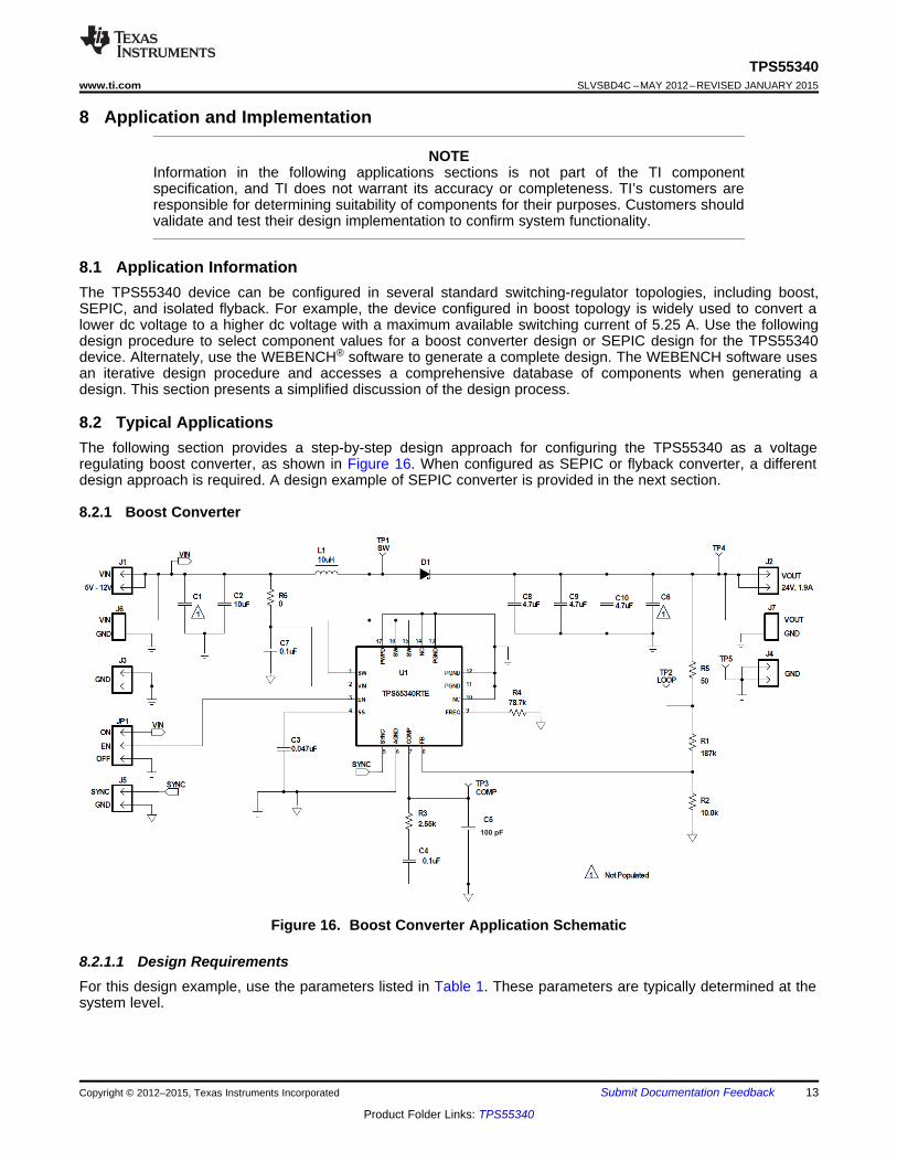
8.2 Typical ApplicationsThe following section provides a step-by-step design approach for configuring the TPS55340 as a voltageregulating boost converter, as shown in Figure 16. When configured as SEPIC or flyback converter, a differentdesign approach is required. A design example of SEPIC converter is provided in the next section.
8.2.1 Boost Converter
Figure 16. Boost Converter Application Schematic
8.2.1.1 Design RequirementsFor this design example, use the parameters listed in Table 1. These parameters are typically determined at thesystem level.
OUT D IN
OUT
V V VD
V VD
+ -=
+
14
TPS55340SLVSBD4C –MAY 2012–REVISED JANUARY 2015 www.ti.com
Product Folder Links: TPS55340
Submit Documentation Feedback Copyright © 2012–2015, Texas Instruments Incorporated
Table 1. Design ParametersPARAMETER VALUE
Output voltage 24 VInput voltage 5 V to 12 VMaximum output current 800 mATransient response 50% load step (ΔVOUT = 3%) 960 mVOutput voltage ripple (0.5% of VOUT) 120 mV
8.2.1.2 Detailed Design Procedure
8.2.1.2.1 Custom Design with WEBENCH Tools
Click here to create a custom design using the TPS55340 device with the WEBENCH® Power Designer.1. Start by entering your VIN, VOUT and IOUT requirements.2. Optimize your design for key parameters like efficiency, footprint and cost using the optimizer dial and
compare this design with other possible solutions from Texas Instruments.3. WEBENCH Power Designer provides you with a customized schematic along with a list of materials with real
time pricing and component availability.4. In most cases, you will also be able to:
– Run electrical simulations to see important waveforms and circuit performance,– Run thermal simulations to understand the thermal performance of your board,– Export your customized schematic and layout into popular CAD formats,– Print PDF reports for the design, and share your design with colleagues.
5. Get more information about WEBENCH tools at www.ti.com/webench.
8.2.1.2.2 Selecting the Switching Frequency (R4)
The first step is to decide on a switching frequency for the regulator. There are tradeoffs to consider for a higheror lower switching frequency. A higher switching frequency allows for lower valued inductor and smaller outputcapacitors leading to the smallest solution size. A lower switching frequency will result in a larger solution sizebut better efficiency. The user will typically set the frequency for the minimum tolerable efficiency to avoidexcessively large external components.
A switching frequency of 600 kHz is a good trade-off between efficiency and solution size. The appropriateresistor value is found from the resistance versus frequency graph of Figure 5, or calculated using Equation 1.R4 is calculated to be 78.4 kΩ and the nearest standard value resistor of 78.7 kΩ is selected. A resistor must beplaced from the FREQ pin to ground, even if an external oscillation is applied for synchronization.
8.2.1.2.3 Determining the Duty Cycle
The input-to-output voltage conversion ratio of the TPS55340 is limited by the worst case maximum duty cycle of89% and the minimum duty cycle which is determined by the minimum on-time of 77 ns and the switchingfrequency. The minimum duty cycle can be estimated with Equation 7. With a 600-kHz switching frequency theminimum duty cycle is 4%.
DPS = TON min × ƒsw (7)
The duty cycle at which the converter operates is dependent on the mode in which the converter is running. If theconverter is running in DCM, where the inductor current ramps to zero at the end of each cycle, the duty cyclevaries with changes of the load much more than it does when running in continuous conduction mode (CCM). InCCM, where the inductor maintains a minimum dc current, the duty cycle is related primarily to the input andoutput voltages as computed below. Assume a 0.5-V drop VD across the Schottky rectifier. At the minimum inputof 5 V, the duty cycle will be 80%. At the maximum input of 12 V, the duty cycle is 51%.
(8)
( )
( )
OUT D IN IN
OUT(crit)
OUT D SW
2
2
V V V VI
2 V V L
+ - ´=
´ + ´ ¦ ´
OUT D IN OUT SW
IN
2 (V V V ) L ID
V
´ + - ´ ´ ´ ¦=
15
TPS55340www.ti.com SLVSBD4C –MAY 2012–REVISED JANUARY 2015
Product Folder Links: TPS55340
Submit Documentation FeedbackCopyright © 2012–2015, Texas Instruments Incorporated
At light loads the converter will operate in DCM. In this case the duty cycle is a function of the load, input andoutput voltages, inductance, and switching frequency as computed below. This can be calculated only after aninductance is chosen in the following section. While operating in DCM with very light load conditions, the dutycycle demand will force the TPS55340 to operate with the minimum on-time. The converter will then begin pulseskipping which can increase the output ripple.
(9)
All converters using a diode as the freewheeling or catch component have a load current level at which theytransit from DCM to CCM. At this point the inductor current just falls to zero during the off-time of the powerswitch. At higher load currents, the inductor current does not fall to zero and diode and switch current assume atrapezoidal wave shape as opposed to a triangular wave shape. The load current boundary betweendiscontinuous conduction and continuous conduction can be found for a set of converter parameters as follows:
(10)
For loads higher than the result of Equation 10, the duty cycle is given by Equation 8. For loads less than theresults of Equation 10, the duty cycle is given by Equation 9. For Equation 7 through Equation 10, the variabledefinitions are as follows:• VOUT is the output voltage of the converter in V.• VD is the forward conduction voltage drop across the rectifier or catch diode in V.• VIN is the input voltage to the converter in V.• IOUT is the output current of the converter in A.• L is the inductor value in H.• ƒSW is the switching frequency in Hz.
Unless otherwise stated, the design equations that follow assume that the converter is running in CCM whichtypically results in a higher efficiency for the power levels of this converter.
8.2.1.2.4 Selecting the Inductor (L1)
The selection of the inductor affects steady-state operation as well as transient behavior and loop stability. Thesefactors make it the most important component in power regulator design. There are three important inductorspecifications: inductor value, dc resistance and saturation current. Considering inductor value alone is notenough. Inductor values can have ±20% tolerance with no current bias. When the inductor current approachessaturation level, the effective inductance can fall to a fraction of the zero current value.
The minimum value of the inductor should be able to meet the inductor current ripple (ΔIL) requirement at worstcase. In a boost converter, maximum inductor current ripple occurs at 50% duty cycle. For the applications whereduty cycle is always smaller or larger than 50%, Equation 12 should be used with the duty cycle closest to 50%and corresponding input voltage to calculate the minimum inductance. For applications that must operate with50% duty cycle when input voltage is somewhere between the minimum and the maximum input voltage,Equation 13 should be used. KIND is a coefficient that represents the amount of inductor ripple current relative tothe maximum input current (IINDC = ILavg). The maximum input current can be estimated with Equation 11, withan estimated efficiency based on similar applications (ηEST). The inductor ripple current will be filtered by theoutput capacitor. Therefore, choosing high inductor ripple currents will impact the selection of the outputcapacitor because the output capacitor must have a ripple current rating equal to or greater than the inductorripple current. In general, the inductor ripple value (KIND) is at the discretion of the designer. However, thefollowing guidelines may be used.
For CCM operation, it is recommended to use KIND values in the range of 0.2 to 0.4. Choosing KIND closer to 0.2results in a larger inductance value, maximizes the potential output current of the converter and minimizes EMI.Choosing KIND closer to 0.4 results in a smaller inductance value, a physically smaller inductor, and improvedtransient response, but potentially worse EMI and lower efficiency. Using an inductor with a smaller inductancevalue may result in the converter operating in DCM. This reduces the maximum output current of the boost
L INDIN LIM EST IN LIM EST
OUT
OUT OUT
I KV min I V min I 1
2 2I max
V V
Dæ ö æ ö´ - ´ h ´ ´ - ´ hç ÷ ç ÷
è ø è ø= =
LL IN
II peak I DC
2
D= +
( )L
L IN
22 I
I rms I DC12
Dæ ö= + ç ÷
è ø
INL
O SW
V min DmaxI
LD = ´
¦
( )OUT D
O
IN IND SW
V V 1L min
I DC K 4
+³ ´
´ ´ ¦, D=50%
INO
IN IND SW
V DL min
I DC K³ ´
´ ¦, D 50%, V with D closest to 50%≠
IN
OUT OUTIN
EST IN
V II DC
V min
´=
h ´
16
TPS55340SLVSBD4C –MAY 2012–REVISED JANUARY 2015 www.ti.com
Product Folder Links: TPS55340
Submit Documentation Feedback Copyright © 2012–2015, Texas Instruments Incorporated
converter, causes larger input voltage and output voltage ripple, and reduced efficiency. For this design, chooseKIND = 0.3 and a conservative efficiency estimate of 85% with the minimum input voltage and maximum outputcurrent. Equation 12 is used with the maximum input voltage because this corresponds to duty cycle closest to50%. The maximum input current is estimated at 4.52 A and the minimum inductance is 7.53 µH. A standardvalue of 10 µH is chosen.
(11)
(12)
(13)
After choosing the inductance, the required current ratings can be calculated. The inductor will be closest to itsratings with the minimum input voltage. The ripple with the chosen inductance is calculated with Equation 14.The RMS and peak inductor current can be found with Equation 15 and Equation 16. For this design the currentripple is 663 mA, the RMS inductor current is 4.52 A, and the peak inductor current is 4.85 A. It is generallyrecommended for the peak inductor current rating of the selected inductor be 20% higher to account fortransients during powerup, faults, or transient load conditions. The most conservative approach is to specify aninductor with a saturation current greater than the maximum peak current limit of the TPS55340. This helps toavoid saturation of the inductor. The chosen inductor is a Würth Elektronik 74437368100. It has a saturationcurrent rating of 12.5 A, RMS current rating of 5.2 A, and typical DCR of 27.0 mΩ.
(14)
(15)
(16)
The TPS55340 has built-in slope compensation to avoid subharmonic oscillation associated with current modecontrol. If the inductor value is too small, the slope compensation may not be adequate, and the loop can beunstable.
8.2.1.2.5 Computing the Maximum Output Current
The overcurrent limit for the integrated power MOSFET limits the maximum input current and thus the maximuminput power for a given input voltage. Maximum output power is less than maximum input power due to powerconversion losses. Therefore, the current limit setting, input voltage, output voltage, and efficiency can all changemaximum current output (IOUTmax). The current limit clamps the peak inductor current; therefore, the ripple hasto be subtracted to derive maximum dc current. Decreasing the KIND or designing for a higher efficiency willincrease the maximum output current. This can be evaluated with the chosen inductance or the chosen KIND.This should be evaluated with the minimum input voltage and minimum peak current limit (ILIM) of 5.25 A.
(17)
In this design with a 5-V input boosted to a 24-V output and a 10-μH inductor with an assumed Schottky forwardvoltage of 0.5 V and estimated efficiency of 85%, the maximum output current is 871 mA. With the 12-V inputand increased estimated efficiency of 90%, the maximum output current increases to 2.13 A. This circuit wasevaluated to its maximum output currents with both the minimum and maximum input voltage.
I L CINSW IN
ILVripple I R4 C
D
= + D ´´ ¦ ´
LCI
II rms
12
D=
( )CO OUT
DmaxI rms I
1 Dmax=
-
TRANOUT
BW TRAN
IC
2 V
D³
´ p ´ ¦ ´ D
OUTRIPPLE
SW OUT
L
Dmax IV
CESR
I
æ ö´-ç ÷
¦ ´è ø£
D
OUTOUT
SW RIPPLE
Dmax IC
V
´³
¦ ´
17
TPS55340www.ti.com SLVSBD4C –MAY 2012–REVISED JANUARY 2015
Product Folder Links: TPS55340
Submit Documentation FeedbackCopyright © 2012–2015, Texas Instruments Incorporated
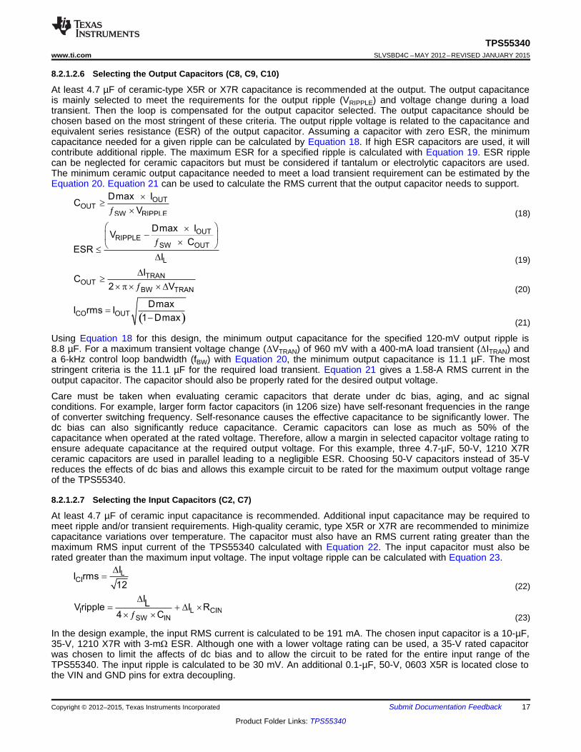
8.2.1.2.6 Selecting the Output Capacitors (C8, C9, C10)
At least 4.7 µF of ceramic-type X5R or X7R capacitance is recommended at the output. The output capacitanceis mainly selected to meet the requirements for the output ripple (VRIPPLE) and voltage change during a loadtransient. Then the loop is compensated for the output capacitor selected. The output capacitance should bechosen based on the most stringent of these criteria. The output ripple voltage is related to the capacitance andequivalent series resistance (ESR) of the output capacitor. Assuming a capacitor with zero ESR, the minimumcapacitance needed for a given ripple can be calculated by Equation 18. If high ESR capacitors are used, it willcontribute additional ripple. The maximum ESR for a specified ripple is calculated with Equation 19. ESR ripplecan be neglected for ceramic capacitors but must be considered if tantalum or electrolytic capacitors are used.The minimum ceramic output capacitance needed to meet a load transient requirement can be estimated by theEquation 20. Equation 21 can be used to calculate the RMS current that the output capacitor needs to support.
(18)
(19)
(20)
(21)
Using Equation 18 for this design, the minimum output capacitance for the specified 120-mV output ripple is8.8 µF. For a maximum transient voltage change (ΔVTRAN) of 960 mV with a 400-mA load transient (ΔITRAN) anda 6-kHz control loop bandwidth (fBW) with Equation 20, the minimum output capacitance is 11.1 µF. The moststringent criteria is the 11.1 µF for the required load transient. Equation 21 gives a 1.58-A RMS current in theoutput capacitor. The capacitor should also be properly rated for the desired output voltage.
Care must be taken when evaluating ceramic capacitors that derate under dc bias, aging, and ac signalconditions. For example, larger form factor capacitors (in 1206 size) have self-resonant frequencies in the rangeof converter switching frequency. Self-resonance causes the effective capacitance to be significantly lower. Thedc bias can also significantly reduce capacitance. Ceramic capacitors can lose as much as 50% of thecapacitance when operated at the rated voltage. Therefore, allow a margin in selected capacitor voltage rating toensure adequate capacitance at the required output voltage. For this example, three 4.7-µF, 50-V, 1210 X7Rceramic capacitors are used in parallel leading to a negligible ESR. Choosing 50-V capacitors instead of 35-Vreduces the effects of dc bias and allows this example circuit to be rated for the maximum output voltage rangeof the TPS55340.
8.2.1.2.7 Selecting the Input Capacitors (C2, C7)
At least 4.7 µF of ceramic input capacitance is recommended. Additional input capacitance may be required tomeet ripple and/or transient requirements. High-quality ceramic, type X5R or X7R are recommended to minimizecapacitance variations over temperature. The capacitor must also have an RMS current rating greater than themaximum RMS input current of the TPS55340 calculated with Equation 22. The input capacitor must also berated greater than the maximum input voltage. The input voltage ripple can be calculated with Equation 23.
(22)
(23)
In the design example, the input RMS current is calculated to be 191 mA. The chosen input capacitor is a 10-µF,35-V, 1210 X7R with 3-mΩ ESR. Although one with a lower voltage rating can be used, a 35-V rated capacitorwas chosen to limit the affects of dc bias and to allow the circuit to be rated for the entire input range of theTPS55340. The input ripple is calculated to be 30 mV. An additional 0.1-µF, 50-V, 0603 X5R is located close tothe VIN and GND pins for extra decoupling.
OUT
OUT OUT
2
2 R C¦ »
p ´ ´
OUTVR1 R2 1
1.229 V
æ ö= ´ -ç ÷
è ø
OUT
R1V 1.229 V 1
R2
æ ö= ´ +ç ÷
è ø
18
TPS55340SLVSBD4C –MAY 2012–REVISED JANUARY 2015 www.ti.com
Product Folder Links: TPS55340
Submit Documentation Feedback Copyright © 2012–2015, Texas Instruments Incorporated
8.2.1.2.8 Setting Output Voltage (R1, R2)
To set the output voltage in either DCM or CCM, select the values of R1 and R2 according to the followingequations:
(24)
(25)
Considering the leakage current through the resistor divider and noise decoupling into the FB pin, an optimumvalue for R2 is around 10 kΩ. The output voltage tolerance depends on the VFB accuracy and the tolerance of R1and R2. In this example with a 24-V output using Equation 25, R1 is calculated to 185.3 kΩ. The neareststandard value of 187 kΩ is used.
8.2.1.2.9 Setting the Soft-start Time (C7)
Choose the appropriate capacitor to set soft-start time and avoid overshoot. Increasing the soft-start timereduces the overshoot during startup. A 0.047-µF ceramic capacitor is used in this example.
8.2.1.2.10 Selecting the Schottky Diode (D1)
The high switching frequency of the TPS55340 demands high-speed rectification for optimum efficiency. Ensurethat the average and peak current ratings of the diode exceed the average output current and peak inductorcurrent. In addition, the reverse breakdown voltage of the diode must exceed the regulated output voltage. Thediode must also be rated for the power dissipated which can be calculated with Equation 26.
PD = VD × IOUT (26)
In this conservative design example, the diode is chosen to be rated for the maximum output current of 2.13 A.During normal operation with 800-mA output current and assuming a Schottky diode drop of 0.5 V, the diodemust be capable of dissipating 400 mW. The recommended minimum ratings for this design are a 40-V, 3-Adiode. However, to improve the flexibility of this design, a Diodes Inc B540-13-F in an SMC package is used withvoltage and current ratings of 40 V and 5 A.
8.2.1.2.11 Compensating the Control Loop (R3, C4, C5)
The TPS55340 requires external compensation which allows the loop response to be optimized for eachapplication. The COMP pin is the output of the internal error amplifier. An external resistor R3 and ceramiccapacitor C4 are connected to the COMP pin to provide a pole and a zero, shown in Figure 16. This pole andzero, along with the inherent pole and zero of a boost converter, determine the closed-loop frequency response.This is important for converter stability and transient response. Loop compensation should be designed for theminimum operating voltage.
The following equations summarize the loop equations for the TPS55340 configured as a CCM boost converter.They include the power stage output pole (ƒOUT) and the right-half-plane zero (ƒRHPZ) of a boost convertercalculated with Equation 27 and Equation 28, respectively. When calculating ƒOUT, it is important to include thederating of ceramic output capacitors. In the example with an estimated 10.2-µF capacitance, these frequenciesare calculated to be 980 kHz and 22.1 kHz, respectively. The dc gain (A) of the power stage is calculated withEquation 27 and is 39.9 dB in this design. The compensation pole (ƒP) and zero (ƒZ) generated by R3, C4, andinternal transconductance amplifier are calculated with Equation 30 and Equation 31, respectively.
Most CCM boost converters will have a stable control loop if fZ is set slightly above ƒP through proper sizing ofR3 and C4. A good starting point is C4 = 0.1 µF and R3 = 2 kΩ. Increasing R3 or reducing C4 increases theclosed-loop bandwidth, and therefore improves the transient response. Adjusting R3 and C4 in the oppositedirection increases the phase and gain margin of the loop, which improves loop stability. It is generallyrecommended to limit the bandwidth of the loop to the lower of either 1/5 of the switching frequency ƒSW or 1/3the RHPZ frequency, ƒRHPZ shown in Equation 28. The spreadsheet tool located in the TPS55340 product folderat www.ti.com can also be used to aid in compensation design.
(27)
co2RHPZ
3
¦¦ =
co1SW
5
¦¦ =
Z
1
2 R3 C4¦ =
p ´ ´
P
1
2 10M C4¦ =
p ´ W ´
eaIN
OUT
OUT OUT SENSE
V1.229 1A G 10M R
V V R 2= ´ ´ W ´ ´ ´
´
OUT INRHPZ
OUT
2R V
2 L V
æ ö¦ » ´ ç ÷
p ´ è ø
19
TPS55340www.ti.com SLVSBD4C –MAY 2012–REVISED JANUARY 2015
Product Folder Links: TPS55340
Submit Documentation FeedbackCopyright © 2012–2015, Texas Instruments Incorporated
(28)
(29)
(30)
(31)
(32)
(33)
100 1k 10k 100k−60
−40
−20
0
20
40
60
−180
−150
−120
−90
−60
−30
0
Frequency (Hz)
Gai
n (d
B)
GainPhase
G016
FF
REFZFF
OUT
1C
V2 R1
V
=
p ´ ´ ¦ ´
ESR OUTR CC5
R3
´=
ZESR
ESR OUT
1
2 R C¦ »
p ´ ´
P2
1
2 R3 C5¦ =
p ´ ´
20
TPS55340SLVSBD4C –MAY 2012–REVISED JANUARY 2015 www.ti.com
Product Folder Links: TPS55340
Submit Documentation Feedback Copyright © 2012–2015, Texas Instruments Incorporated
Where• COUT is the equivalent output capacitor (COUT= C8 + C9 + C10)• ROUT is the equivalent load resistance (VOUT/IOUT)• Gea is the error amplifier transconductance located in Electrical Characteristics• RSENSE (15 mΩ, typical) is the sense resistor in the current control loop• ƒco1 and ƒco2 are possible bandwidths.
An additional capacitor from the COMP pin to GND (C5) can be used to place a high-frequency pole in thecontrol loop. This is not always necessary with ceramic output capacitors. If a nonceramic output capacitor isused, there is an additional zero (fZESR) in the control loop which can be calculated with Equation 35. The valueof C5 and the pole created by C5 can be calculated with Equation 36 and Equation 34, respectively. Finally, ifmore phase margin is needed, an additional zero (fZFF) can be added by placing a capacitor (CFF) in parallel withthe top feedback resistor R1. It is recommended to place the zero at the target cross-over frequency or higher.The feed-forward capacitor also adds a pole at a higher frequency. The recommended value of CFF can becalculated with Equation 37.
(34)
(35)
(36)
(37)
where RESR is the ESR of the output capacitor.
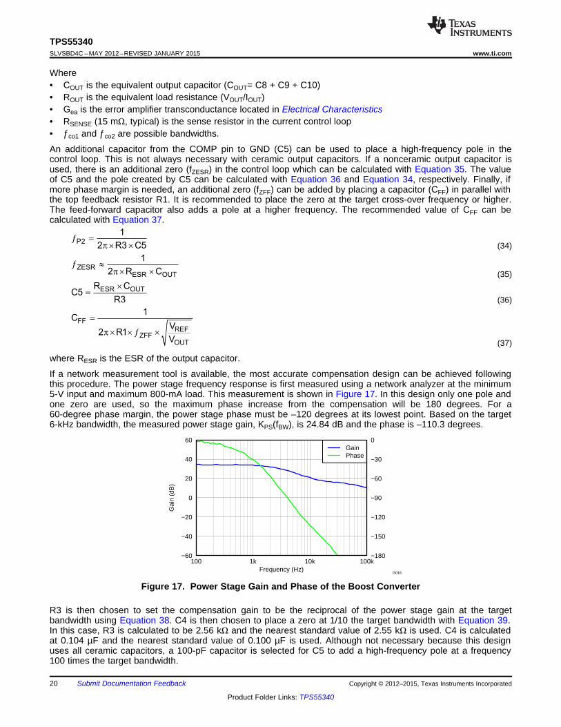
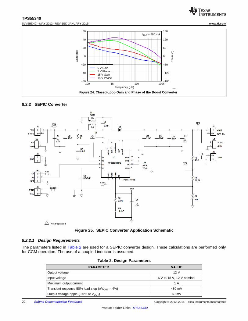
If a network measurement tool is available, the most accurate compensation design can be achieved followingthis procedure. The power stage frequency response is first measured using a network analyzer at the minimum5-V input and maximum 800-mA load. This measurement is shown in Figure 17. In this design only one pole andone zero are used, so the maximum phase increase from the compensation will be 180 degrees. For a60-degree phase margin, the power stage phase must be –120 degrees at its lowest point. Based on the target6-kHz bandwidth, the measured power stage gain, KPS(fBW), is 24.84 dB and the phase is –110.3 degrees.
Figure 17. Power Stage Gain and Phase of the Boost Converter
R3 is then chosen to set the compensation gain to be the reciprocal of the power stage gain at the targetbandwidth using Equation 38. C4 is then chosen to place a zero at 1/10 the target bandwidth with Equation 39.In this case, R3 is calculated to be 2.56 kΩ and the nearest standard value of 2.55 kΩ is used. C4 is calculatedat 0.104 µF and the nearest standard value of 0.100 µF is used. Although not necessary because this designuses all ceramic capacitors, a 100-pF capacitor is selected for C5 to add a high-frequency pole at a frequency100 times the target bandwidth.
V (ac coupled) = 20mV/divOUT
I = 200mA/divL
SW = 20V/div
Time - 50 s/divm
V = 1V/divIN
EN = 2V/div
V = 10V/divOUT
SW = 10V/div
Time - 500 s/divm
V (ac coupled) = 100mV/divOUT
SW = 20V/div
I = 1A/divL
Time - 1ms/div
V (ac coupled) = 10mV/divOUT
I = 1A/divL
SW = 20V/div
Time - 1 s/divm
50
55
60
65
70
75
80
85
90
95
100
0 0.4 0.8 1.2 1.6 2Output Current (A)
Effi
cien
cy (
%)
VIN = 5 VVIN = 12 V
G017
I = 200mA/divOUT
Time - 1ms/div
V (ac coupled) = 500mV/divOUT
BW
1C4
2 R310
=¦
p ´ ´
( )
( )KPS BW
20
1R3
R2Gea 10
R1 R2
¦
=æ ö
ç ÷´ ´ç ÷+è ø
21
TPS55340www.ti.com SLVSBD4C –MAY 2012–REVISED JANUARY 2015
Product Folder Links: TPS55340
Submit Documentation FeedbackCopyright © 2012–2015, Texas Instruments Incorporated
(38)
(39)
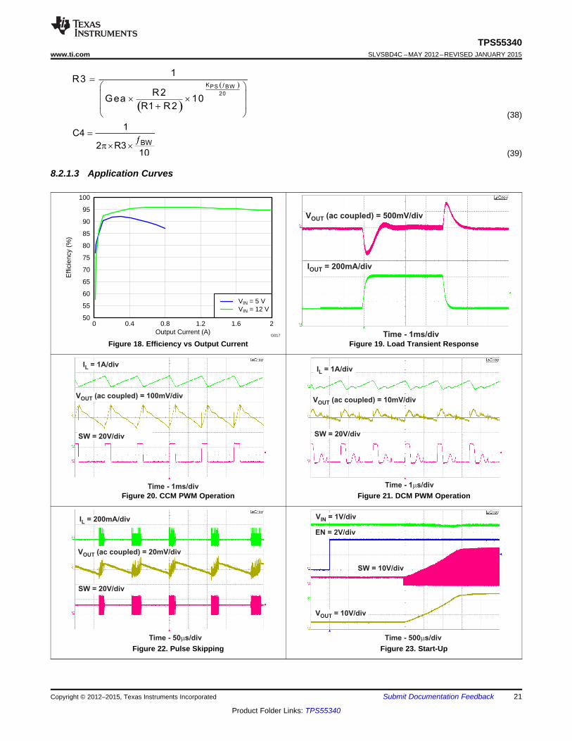
8.2.1.3 Application Curves
Figure 18. Efficiency vs Output Current Figure 19. Load Transient Response
Figure 20. CCM PWM Operation Figure 21. DCM PWM Operation
Figure 22. Pulse Skipping Figure 23. Start-Up
VIN
6-18V
VIN
VIN
12V, 1A
49.9
86.6k
1
1 Not Populated
TP3
SYNC
SYNC
TP2
TP5
TP4
Lb
La
100 1k 10k 100k−60
−40
−20
0
20
40
60
−180
−120
−60
0
60
120
180
Frequency (Hz)
Gai
n (d
B)
Pha
se (
°)
5 V Gain5 V Phase15 V Gain15 V Phase
IOUT = 800 mA
G023
22
TPS55340SLVSBD4C –MAY 2012–REVISED JANUARY 2015 www.ti.com
Product Folder Links: TPS55340
Submit Documentation Feedback Copyright © 2012–2015, Texas Instruments Incorporated
Figure 24. Closed-Loop Gain and Phase of the Boost Converter
8.2.2 SEPIC Converter
Figure 25. SEPIC Converter Application Schematic
8.2.2.1 Design RequirementsThe parameters listed in Table 2 are used for a SEPIC converter design. These calculations are performed onlyfor CCM operation. The use of a coupled inductor is assumed.
Table 2. Design ParametersPARAMETER VALUE
Output voltage 12 VInput voltage 6 V to 18 V, 12 V nominalMaximum output current 1 ATransient response 50% load step (ΔVOUT = 4%) 480 mVOutput voltage ripple (0.5% of VOUT) 60 mV
TRANOUT
BW TRAN
IC
2 V
D³
p ´ ¦ ´ D
OUTOUT
SW RIPPLE
Dmax IC
V
´³
¦ ´
( ) ( )LIM L LIM IN IND
OUT
OUT OUT
IN EST IN EST
I I I I DC KI max
V V1 1
V min V min
- D - ´= =
æ ö æ ö+ +ç ÷ ç ÷
´ h ´ hè ø è ø
L Lpeak peak DCL La Lb IN OUT
I II peak I I I I
2 2
D Dæ ö æ ö= + = + + +ç ÷ ç ÷
è ø è ø
INL
SW
V max DminI
2 L
´D =
´ ¦ ´
IN
SW IN IND
V max DminL
2 I DC K
´³
´ ¦ ´ ´
OUT D
OUT D IN
V VD
V V V
+=
+ +
23
TPS55340www.ti.com SLVSBD4C –MAY 2012–REVISED JANUARY 2015
Product Folder Links: TPS55340
Submit Documentation FeedbackCopyright © 2012–2015, Texas Instruments Incorporated
8.2.2.2 Detailed Design Procedure
8.2.2.2.1 Selecting the Switching Frequency (R4)
A 500-kHz switching frequency (ƒSW) is selected for this design. Using Equation 1, R4 is calculated and thenearest standard value of 95.3 kΩ is used.
8.2.2.2.2 Duty Cycle
The duty cycle of a SEPIC converter is calculated with Equation 40. With the 6-V minimum input voltage, theduty cycle is 68%; and with the 18-V maximum input voltage, the duty cycle is 41%.
(40)
8.2.2.2.3 Selecting the Inductor (L1)
With an estimated 85% efficiency, the input current is calculated with Equation 9 to be 2.35 A. With KIND of 0.3and the maximum 18-V input voltage, the minimum inductance is calculated to be 10.5 µH using Equation 41.The nearest standard value of 12 µH is used. As mentioned previously, this equation assumes a coupledinductor is used.
(41)
The inductor ripple current is recalculated to be 615 mA with Equation 42. The peak current is calculated to be3.69 A. The typical current limit is used as the saturation rating for the inductor used. The RMS current for La isapproximately the average input current of 2.35 A. The RMS current for Lb is approximately the output current of1 A. For this design, a CoilCraft MSD1260-123 is used with 6.86-A saturation, 74-mΩ DCR, and 3.12-A RMScurrent rating for one winding.
(42)
(43)
8.2.2.2.4 Calculating the Maximum Output Current
The maximum output current with the minimum input voltage 6 V, chosen inductance 12 µH, 5.25-A minimumcurrent limit, and estimated 85% efficiency is calculated to be 1.47 A using Equation 44.
(44)
8.2.2.2.5 Selecting the Output Capacitors (C8, C9, C10)
To meet the 60-mV ripple specification, the minimum output capacitance is calculated to be 22.5 µF withEquation 45. This design uses ceramic output capacitors and the effects of ESR are ignored. To meet thetransient response of 500 mA with less than 480-mV voltage change and a 7-kHz control loop bandwidth, theminimum output capacitance is calculated to be 23.7 µF using Equation 46. The RMS current is calculated withEquation 22 to be 1.44 A. The output capacitors used in this design are 3 × 22 µF, 25 V, X7R 1210 ceramiccapacitors. With voltage derating, the effective total output capacitance is estimated to be 30.4 µF.
(45)
(46)
( )
OUT
OUTRHPZ
2
V
I
D2 L
1 D
¦ =
æ ö
´ p ´ ´ ç ÷ç ÷-è ø
LCI
II rms
12
D=
LrippleI
SW IN
IV
4 C
D=
´ ¦ ´
CP IN
(1 Dmax)I rms I DC
Dmax
-= ´
OUTP
IN SW
I DmaxC
0.05 V max ƒ
´³
´ ´
24
TPS55340SLVSBD4C –MAY 2012–REVISED JANUARY 2015 www.ti.com
Product Folder Links: TPS55340
Submit Documentation Feedback Copyright © 2012–2015, Texas Instruments Incorporated
8.2.2.2.6 Selecting the Series Capacitor (C6)
The series capacitor is chosen to limit the ripple current to 5% of the maximum input voltage. Using Equation 47the minimum capacitance is 1.5 µF. Using Equation 48 the RMS current is calculated to be 1.63 A. A 2.2-µFceramic capacitor in a 1206 package is selected.
(47)
(48)
8.2.2.2.7 Selecting the Input Capacitor (C2, C7)
Based on the minimum 4.7-µF ceramic recommended for the TPS55340, a 10-µF X7R input capacitor is usedwith an additional 0.1 µF placed close to the VIN and GND pins. With an estimated 6-µF capacitance aftervoltage derating, the input ripple voltage is calculated to be 39.9 mV using Equation 49. The RMS current of theinput capacitance is calculated to be 0.177 A with Equation 50.
(49)
(50)
8.2.2.2.8 Selecting the Schottky Diode (D1)
The selected diode must have a minimum breakdown voltage (VBR) calculated with Equation 51 which is 30.5 Vin this design. The average current rating is recommended to be greater than the maximum output current. Withthe maximum 18-V input, average current is calculated to be 2.6 A using Equation 17. The package must also becapable of handling the power dissipation. With an estimated 0.5-V forward voltage, power dissipation iscalculated with Equation 26 to be 500 mW. Diodes Inc B340B is chosen with a 40-V, 3-A rating in an SMBpackage.
VBR = VO + VINmax + VF (51)
8.2.2.2.9 Setting the Output Voltage (R1, R2)
With R2 fixed at 10 kΩ using Equation 25 the nearest standard value of 86.6 kΩ is chosen for R1.
8.2.2.2.10 Setting the Soft-start Time (C3)
The recommended 0.047-µF soft-start capacitor is used.
8.2.2.2.11 MOSFET Rating Considerations
In a SEPIC converter the MOSFET must be rated to handle the sum of the input and output voltages. In thisdesign with the maximum input voltage of 18 V and output voltage of 12 V, the FET will see approximately 30 V.A 10% tolerance is recommended to account for any ringing. The 40-V rating of the TPS55340 power MOSFETcomfortably satisfies this requirement.
8.2.2.2.12 Compensating the Control Loop (R3, C4)
This design was compensated by measuring the frequency response of the power stage at the lowest inputvoltage of 6 V and choosing the components for the desired bandwidth. The lowest right half plane zero (ƒRHPZ)is calculated to be 36.7 kHz with Equation 52. Using the recommendation to limit the bandwidth to 1/3 of ƒRHPZ,the maximum recommended is 12.2 kHz.
(52)
100 1k 10k 100k−60
−40
−20
0
20
40
60
−180
−120
−60
0
60
120
180
Frequency (Hz)
Gai
n (d
B)
Pha
se (
°)
6 V Input Gain6 V Input Phase
G025
25
TPS55340www.ti.com SLVSBD4C –MAY 2012–REVISED JANUARY 2015
Product Folder Links: TPS55340
Submit Documentation FeedbackCopyright © 2012–2015, Texas Instruments Incorporated
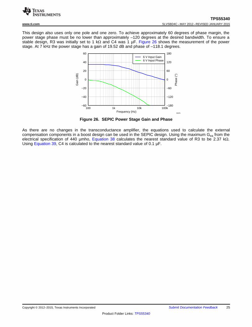
This design also uses only one pole and one zero. To achieve approximately 60 degrees of phase margin, thepower stage phase must be no lower than approximately –120 degrees at the desired bandwidth. To ensure astable design, R3 was initially set to 1 kΩ and C4 was 1 µF. Figure 26 shows the measurement of the powerstage. At 7 kHz the power stage has a gain of 19.52 dB and phase of –118.1 degrees.
Figure 26. SEPIC Power Stage Gain and Phase
As there are no changes in the transconductance amplifier, the equations used to calculate the externalcompensation components in a boost design can be used in the SEPIC design. Using the maximum Gea from theelectrical specification of 440 µmho, Equation 38 calculates the nearest standard value of R3 to be 2.37 kΩ.Using Equation 39, C4 is calculated to the nearest standard value of 0.1 µF.
100 1k 10k 100k−60
−40
−20
0
20
40
60
−180
−120
−60
0
60
120
180
Frequency (Hz)
Gai
n (d
B)
Pha
se (
°)
6 V Gain6 V Phase18 V Gain18 V Phase
G030
V (ac coupled) = 50mV/divOUT
I = 1A/divLa
I = 1A/divLb
SW = 10V/div
Time - 2 s/divm
V = 5V/divOUT
V = 2V/divIN
EN = 2V/divSW = 20V/div
Time - 1ms/div
V (ac coupled) = 200mV/divOUT
I = 500mA/divOUT
Time - 500 s/divm
50
55
60
65
70
75
80
85
90
95
100
0 0.2 0.4 0.6 0.8 1 1.2Output Current (A)
Effi
cien
cy (
%)
VIN = 6 VVIN = 12 VVIN = 18 V
G026
26
TPS55340SLVSBD4C –MAY 2012–REVISED JANUARY 2015 www.ti.com
Product Folder Links: TPS55340
Submit Documentation Feedback Copyright © 2012–2015, Texas Instruments Incorporated
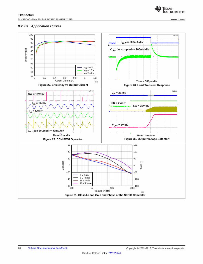
8.2.2.3 Application Curves
Figure 27. Efficiency vs Output Current Figure 28. Load Transient Response
Figure 29. CCM PWM Operation Figure 30. Output Voltage Soft-start
Figure 31. Closed-Loop Gain and Phase of the SEPIC Converter
LO
Output
Filter
Capacitor
VOVI
Power Ground
Power Ground
VI
Bypass
Capacitor
VI
High-Frequency
Bypass Capacitor
C(SS)
CI
Feedback
Resistors
Frequency
Set
Resistor
Connect to VO on the
inner or bottom layer
Connect to AGND on the
inner or bottom layer
Output
Filter
Capacitor
Compensation
Network
UVLO
Resistors
Bypass capacitor
for TPS55340.
Put close to Pin 29
10
12
11
4
3
1
2
5 6 87
SW
16 15 1314
PowerPad
SW NC PGND
SYNC AGND COMP FB
SS
EN
VIN
SW
FREQ
NC
PGND
PGND
27
TPS55340www.ti.com SLVSBD4C –MAY 2012–REVISED JANUARY 2015
Product Folder Links: TPS55340
Submit Documentation FeedbackCopyright © 2012–2015, Texas Instruments Incorporated
9 Power Supply RecommendationsThe device is designed to operate from an input voltage supply range between 2.9 V and 32 V. This input supplymust be well regulated. If the input supply is located more than a few inches from the TPS55340 converteradditional bulk capacitance may be required in addition to the ceramic bypass capacitors. An electrolyticcapacitor with a value of 100 μF is a typical choice.
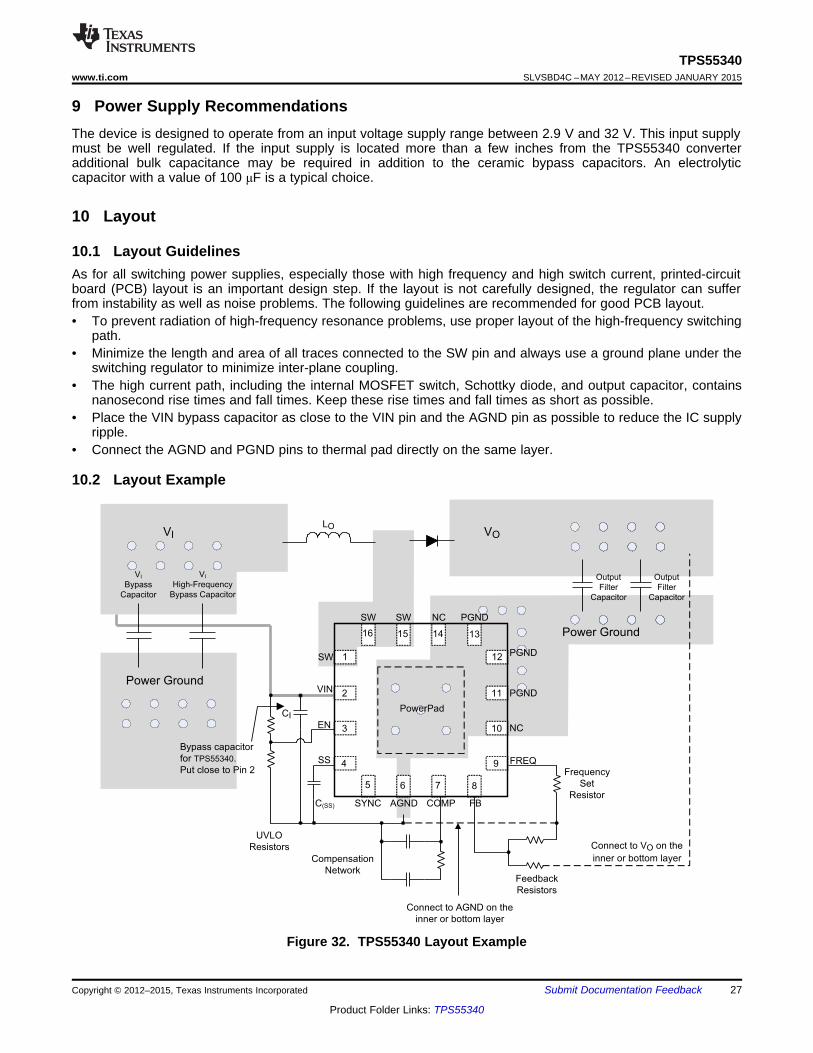
10 Layout
10.1 Layout GuidelinesAs for all switching power supplies, especially those with high frequency and high switch current, printed-circuitboard (PCB) layout is an important design step. If the layout is not carefully designed, the regulator can sufferfrom instability as well as noise problems. The following guidelines are recommended for good PCB layout.• To prevent radiation of high-frequency resonance problems, use proper layout of the high-frequency switching
path.• Minimize the length and area of all traces connected to the SW pin and always use a ground plane under the
switching regulator to minimize inter-plane coupling.• The high current path, including the internal MOSFET switch, Schottky diode, and output capacitor, contains
nanosecond rise times and fall times. Keep these rise times and fall times as short as possible.• Place the VIN bypass capacitor as close to the VIN pin and the AGND pin as possible to reduce the IC supply
ripple.• Connect the AGND and PGND pins to thermal pad directly on the same layer.
10.2 Layout Example
Figure 32. TPS55340 Layout Example
28
TPS55340SLVSBD4C –MAY 2012–REVISED JANUARY 2015 www.ti.com
Product Folder Links: TPS55340
Submit Documentation Feedback Copyright © 2012–2015, Texas Instruments Incorporated
10.3 Thermal ConsiderationsThe maximum IC junction temperature should be restricted to 150°C under normal operating conditions. Thisrestriction limits the power dissipation of the TPS55340. The TPS55340 features a thermally enhanced QFNpackage. This package includes a PowerPAD that improves the thermal capabilities of the package. The thermalresistance of the QFN package in any application greatly depends on the PCB layout and the PowerPADconnection. The PowerPAD must be soldered to the analog ground on the PCB. Use thermal vias underneaththe PowerPAD to achieve good thermal performance.
29
TPS55340www.ti.com SLVSBD4C –MAY 2012–REVISED JANUARY 2015
Product Folder Links: TPS55340
Submit Documentation FeedbackCopyright © 2012–2015, Texas Instruments Incorporated
11 Device and Documentation Support
11.1 Custom Design with WEBENCH ToolsClick here to create a custom design using the TPS55340 device with the WEBENCH® Power Designer.1. Start by entering your VIN, VOUT and IOUT requirements.2. Optimize your design for key parameters like efficiency, footprint and cost using the optimizer dial and
compare this design with other possible solutions from Texas Instruments.3. WEBENCH Power Designer provides you with a customized schematic along with a list of materials with real
time pricing and component availability.4. In most cases, you will also be able to:
– Run electrical simulations to see important waveforms and circuit performance,– Run thermal simulations to understand the thermal performance of your board,– Export your customized schematic and layout into popular CAD formats,– Print PDF reports for the design, and share your design with colleagues.
5. Get more information about WEBENCH tools at www.ti.com/webench.
11.2 Receiving Notification of Documentation UpdatesTo receive notification of documentation updates, navigate to the device product folder on ti.com. In the upperright corner, click on Alert me to register and receive a weekly digest of any product information that haschanged. For change details, review the revision history included in any revised document.
11.3 TrademarksPowerPAD is a trademark of Texas Instruments.WEBENCH is a registered trademark of Texas Instruments.All other trademarks are the property of their respective owners.
11.4 Electrostatic Discharge CautionThese devices have limited built-in ESD protection. The leads should be shorted together or the device placed in conductive foamduring storage or handling to prevent electrostatic damage to the MOS gates.
11.5 GlossarySLYZ022 — TI Glossary.
This glossary lists and explains terms, acronyms, and definitions.
12 Mechanical, Packaging, and Orderable InformationThe following pages include mechanical, packaging, and orderable information. This information is the mostcurrent data available for the designated devices. This data is subject to change without notice and revision ofthis document. For browser-based versions of this data sheet, refer to the left-hand navigation.
PACKAGE OPTION ADDENDUM
www.ti.com 6-Oct-2014
Addendum-Page 1
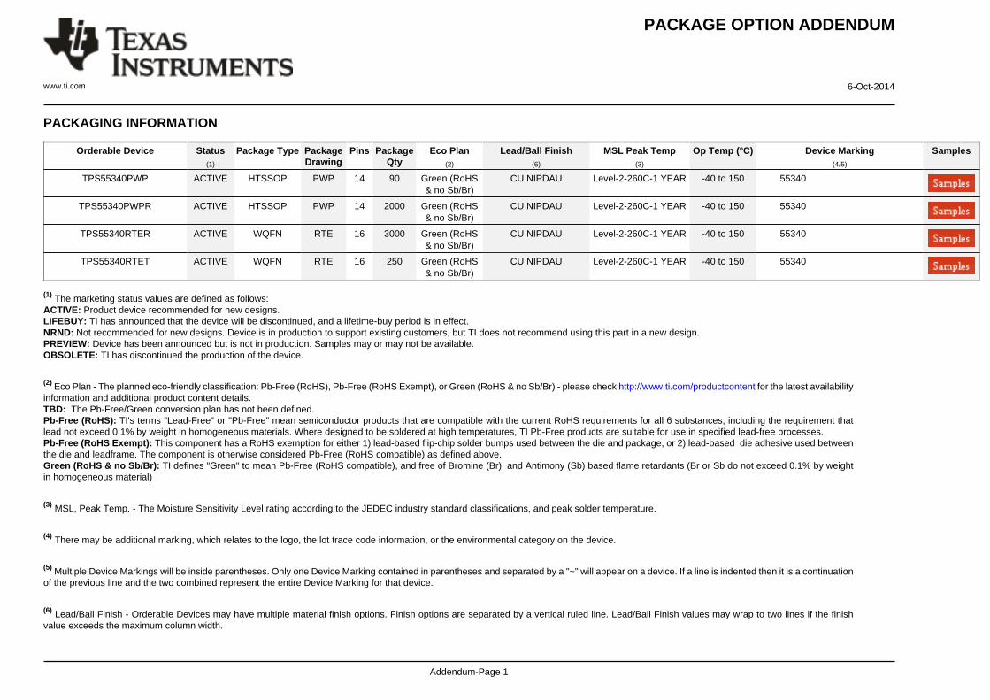
PACKAGING INFORMATION
Orderable Device Status(1)
Package Type PackageDrawing
Pins PackageQty
Eco Plan(2)
Lead/Ball Finish(6)
MSL Peak Temp(3)
Op Temp (°C) Device Marking(4/5)
Samples
TPS55340PWP ACTIVE HTSSOP PWP 14 90 Green (RoHS& no Sb/Br)
CU NIPDAU Level-2-260C-1 YEAR -40 to 150 55340
TPS55340PWPR ACTIVE HTSSOP PWP 14 2000 Green (RoHS& no Sb/Br)
CU NIPDAU Level-2-260C-1 YEAR -40 to 150 55340
TPS55340RTER ACTIVE WQFN RTE 16 3000 Green (RoHS& no Sb/Br)
CU NIPDAU Level-2-260C-1 YEAR -40 to 150 55340
TPS55340RTET ACTIVE WQFN RTE 16 250 Green (RoHS& no Sb/Br)
CU NIPDAU Level-2-260C-1 YEAR -40 to 150 55340
(1) The marketing status values are defined as follows:ACTIVE: Product device recommended for new designs.LIFEBUY: TI has announced that the device will be discontinued, and a lifetime-buy period is in effect.NRND: Not recommended for new designs. Device is in production to support existing customers, but TI does not recommend using this part in a new design.PREVIEW: Device has been announced but is not in production. Samples may or may not be available.OBSOLETE: TI has discontinued the production of the device.
(2) Eco Plan - The planned eco-friendly classification: Pb-Free (RoHS), Pb-Free (RoHS Exempt), or Green (RoHS & no Sb/Br) - please check http://www.ti.com/productcontent for the latest availabilityinformation and additional product content details.TBD: The Pb-Free/Green conversion plan has not been defined.Pb-Free (RoHS): TI's terms "Lead-Free" or "Pb-Free" mean semiconductor products that are compatible with the current RoHS requirements for all 6 substances, including the requirement thatlead not exceed 0.1% by weight in homogeneous materials. Where designed to be soldered at high temperatures, TI Pb-Free products are suitable for use in specified lead-free processes.Pb-Free (RoHS Exempt): This component has a RoHS exemption for either 1) lead-based flip-chip solder bumps used between the die and package, or 2) lead-based die adhesive used betweenthe die and leadframe. The component is otherwise considered Pb-Free (RoHS compatible) as defined above.Green (RoHS & no Sb/Br): TI defines "Green" to mean Pb-Free (RoHS compatible), and free of Bromine (Br) and Antimony (Sb) based flame retardants (Br or Sb do not exceed 0.1% by weightin homogeneous material)
(3) MSL, Peak Temp. - The Moisture Sensitivity Level rating according to the JEDEC industry standard classifications, and peak solder temperature.
(4) There may be additional marking, which relates to the logo, the lot trace code information, or the environmental category on the device.
(5) Multiple Device Markings will be inside parentheses. Only one Device Marking contained in parentheses and separated by a "~" will appear on a device. If a line is indented then it is a continuationof the previous line and the two combined represent the entire Device Marking for that device.
(6) Lead/Ball Finish - Orderable Devices may have multiple material finish options. Finish options are separated by a vertical ruled line. Lead/Ball Finish values may wrap to two lines if the finishvalue exceeds the maximum column width.
PACKAGE OPTION ADDENDUM
www.ti.com 6-Oct-2014
Addendum-Page 2
Important Information and Disclaimer:The information provided on this page represents TI's knowledge and belief as of the date that it is provided. TI bases its knowledge and belief on informationprovided by third parties, and makes no representation or warranty as to the accuracy of such information. Efforts are underway to better integrate information from third parties. TI has taken andcontinues to take reasonable steps to provide representative and accurate information but may not have conducted destructive testing or chemical analysis on incoming materials and chemicals.TI and TI suppliers consider certain information to be proprietary, and thus CAS numbers and other limited information may not be available for release.
In no event shall TI's liability arising out of such information exceed the total purchase price of the TI part(s) at issue in this document sold by TI to Customer on an annual basis.
OTHER QUALIFIED VERSIONS OF TPS55340 :
• Automotive: TPS55340-Q1
• Enhanced Product: TPS55340-EP
NOTE: Qualified Version Definitions:
• Automotive - Q100 devices qualified for high-reliability automotive applications targeting zero defects
• Enhanced Product - Supports Defense, Aerospace and Medical Applications
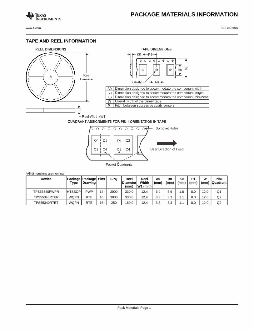
TAPE AND REEL INFORMATION
*All dimensions are nominal
Device PackageType
PackageDrawing
Pins SPQ ReelDiameter
(mm)
ReelWidth
W1 (mm)
A0(mm)
B0(mm)
K0(mm)
P1(mm)
W(mm)
Pin1Quadrant
TPS55340PWPR HTSSOP PWP 14 2000 330.0 12.4 6.9 5.6 1.6 8.0 12.0 Q1
TPS55340RTER WQFN RTE 16 3000 330.0 12.4 3.3 3.3 1.1 8.0 12.0 Q2
TPS55340RTET WQFN RTE 16 250 180.0 12.4 3.3 3.3 1.1 8.0 12.0 Q2
PACKAGE MATERIALS INFORMATION
www.ti.com 13-Feb-2016
Pack Materials-Page 1
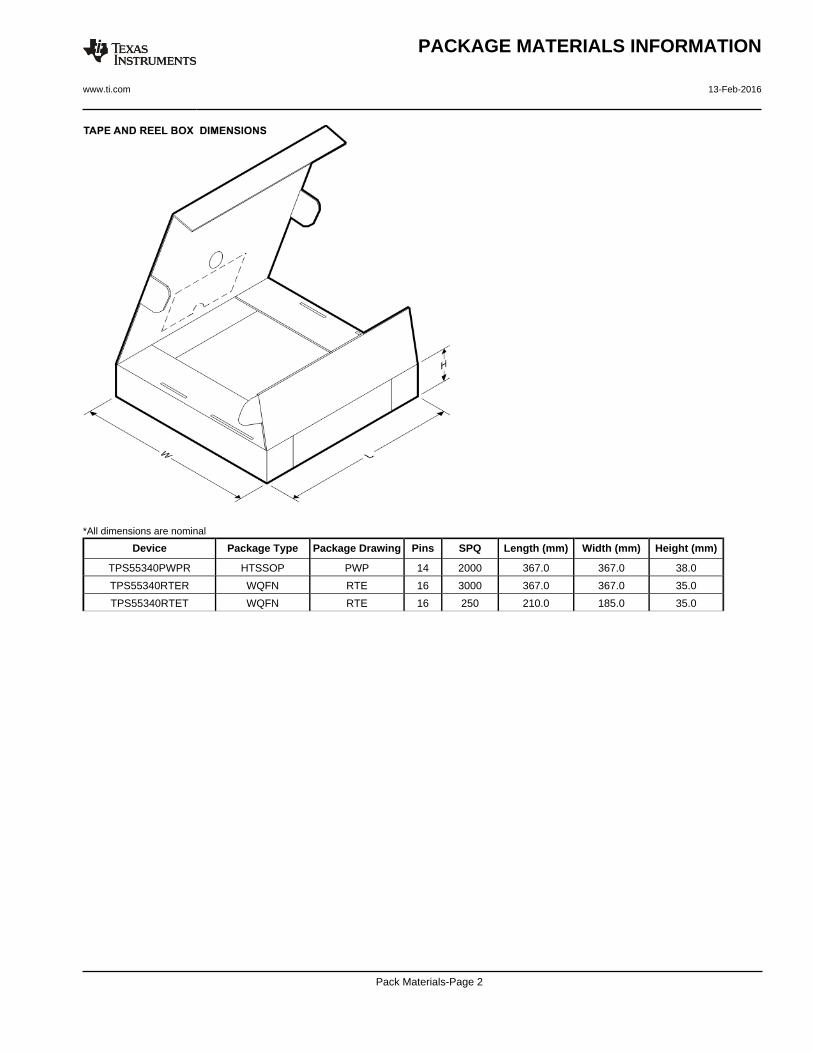
*All dimensions are nominal
Device Package Type Package Drawing Pins SPQ Length (mm) Width (mm) Height (mm)
TPS55340PWPR HTSSOP PWP 14 2000 367.0 367.0 38.0
TPS55340RTER WQFN RTE 16 3000 367.0 367.0 35.0
TPS55340RTET WQFN RTE 16 250 210.0 185.0 35.0
PACKAGE MATERIALS INFORMATION
www.ti.com 13-Feb-2016
Pack Materials-Page 2
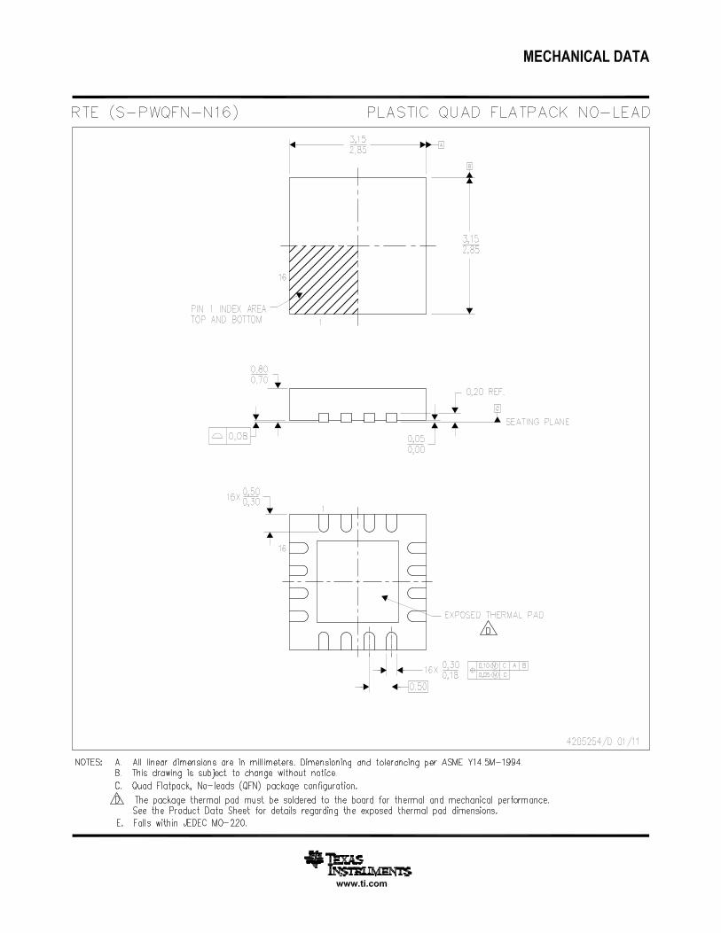
IMPORTANT NOTICE
Texas Instruments Incorporated (TI) reserves the right to make corrections, enhancements, improvements and other changes to itssemiconductor products and services per JESD46, latest issue, and to discontinue any product or service per JESD48, latest issue. Buyersshould obtain the latest relevant information before placing orders and should verify that such information is current and complete.TI’s published terms of sale for semiconductor products (http://www.ti.com/sc/docs/stdterms.htm) apply to the sale of packaged integratedcircuit products that TI has qualified and released to market. Additional terms may apply to the use or sale of other types of TI products andservices.Reproduction of significant portions of TI information in TI data sheets is permissible only if reproduction is without alteration and isaccompanied by all associated warranties, conditions, limitations, and notices. TI is not responsible or liable for such reproduceddocumentation. Information of third parties may be subject to additional restrictions. Resale of TI products or services with statementsdifferent from or beyond the parameters stated by TI for that product or service voids all express and any implied warranties for theassociated TI product or service and is an unfair and deceptive business practice. TI is not responsible or liable for any such statements.Buyers and others who are developing systems that incorporate TI products (collectively, “Designers”) understand and agree that Designersremain responsible for using their independent analysis, evaluation and judgment in designing their applications and that Designers havefull and exclusive responsibility to assure the safety of Designers' applications and compliance of their applications (and of all TI productsused in or for Designers’ applications) with all applicable regulations, laws and other applicable requirements. Designer represents that, withrespect to their applications, Designer has all the necessary expertise to create and implement safeguards that (1) anticipate dangerousconsequences of failures, (2) monitor failures and their consequences, and (3) lessen the likelihood of failures that might cause harm andtake appropriate actions. Designer agrees that prior to using or distributing any applications that include TI products, Designer willthoroughly test such applications and the functionality of such TI products as used in such applications.TI’s provision of technical, application or other design advice, quality characterization, reliability data or other services or information,including, but not limited to, reference designs and materials relating to evaluation modules, (collectively, “TI Resources”) are intended toassist designers who are developing applications that incorporate TI products; by downloading, accessing or using TI Resources in anyway, Designer (individually or, if Designer is acting on behalf of a company, Designer’s company) agrees to use any particular TI Resourcesolely for this purpose and subject to the terms of this Notice.TI’s provision of TI Resources does not expand or otherwise alter TI’s applicable published warranties or warranty disclaimers for TIproducts, and no additional obligations or liabilities arise from TI providing such TI Resources. TI reserves the right to make corrections,enhancements, improvements and other changes to its TI Resources. TI has not conducted any testing other than that specificallydescribed in the published documentation for a particular TI Resource.Designer is authorized to use, copy and modify any individual TI Resource only in connection with the development of applications thatinclude the TI product(s) identified in such TI Resource. NO OTHER LICENSE, EXPRESS OR IMPLIED, BY ESTOPPEL OR OTHERWISETO ANY OTHER TI INTELLECTUAL PROPERTY RIGHT, AND NO LICENSE TO ANY TECHNOLOGY OR INTELLECTUAL PROPERTYRIGHT OF TI OR ANY THIRD PARTY IS GRANTED HEREIN, including but not limited to any patent right, copyright, mask work right, orother intellectual property right relating to any combination, machine, or process in which TI products or services are used. Informationregarding or referencing third-party products or services does not constitute a license to use such products or services, or a warranty orendorsement thereof. Use of TI Resources may require a license from a third party under the patents or other intellectual property of thethird party, or a license from TI under the patents or other intellectual property of TI.TI RESOURCES ARE PROVIDED “AS IS” AND WITH ALL FAULTS. TI DISCLAIMS ALL OTHER WARRANTIES ORREPRESENTATIONS, EXPRESS OR IMPLIED, REGARDING RESOURCES OR USE THEREOF, INCLUDING BUT NOT LIMITED TOACCURACY OR COMPLETENESS, TITLE, ANY EPIDEMIC FAILURE WARRANTY AND ANY IMPLIED WARRANTIES OFMERCHANTABILITY, FITNESS FOR A PARTICULAR PURPOSE, AND NON-INFRINGEMENT OF ANY THIRD PARTY INTELLECTUALPROPERTY RIGHTS. TI SHALL NOT BE LIABLE FOR AND SHALL NOT DEFEND OR INDEMNIFY DESIGNER AGAINST ANY CLAIM,INCLUDING BUT NOT LIMITED TO ANY INFRINGEMENT CLAIM THAT RELATES TO OR IS BASED ON ANY COMBINATION OFPRODUCTS EVEN IF DESCRIBED IN TI RESOURCES OR OTHERWISE. IN NO EVENT SHALL TI BE LIABLE FOR ANY ACTUAL,DIRECT, SPECIAL, COLLATERAL, INDIRECT, PUNITIVE, INCIDENTAL, CONSEQUENTIAL OR EXEMPLARY DAMAGES INCONNECTION WITH OR ARISING OUT OF TI RESOURCES OR USE THEREOF, AND REGARDLESS OF WHETHER TI HAS BEENADVISED OF THE POSSIBILITY OF SUCH DAMAGES.Unless TI has explicitly designated an individual product as meeting the requirements of a particular industry standard (e.g., ISO/TS 16949and ISO 26262), TI is not responsible for any failure to meet such industry standard requirements.Where TI specifically promotes products as facilitating functional safety or as compliant with industry functional safety standards, suchproducts are intended to help enable customers to design and create their own applications that meet applicable functional safety standardsand requirements. Using products in an application does not by itself establish any safety features in the application. Designers mustensure compliance with safety-related requirements and standards applicable to their applications. Designer may not use any TI products inlife-critical medical equipment unless authorized officers of the parties have executed a special contract specifically governing such use.Life-critical medical equipment is medical equipment where failure of such equipment would cause serious bodily injury or death (e.g., lifesupport, pacemakers, defibrillators, heart pumps, neurostimulators, and implantables). Such equipment includes, without limitation, allmedical devices identified by the U.S. Food and Drug Administration as Class III devices and equivalent classifications outside the U.S.TI may expressly designate certain products as completing a particular qualification (e.g., Q100, Military Grade, or Enhanced Product).Designers agree that it has the necessary expertise to select the product with the appropriate qualification designation for their applicationsand that proper product selection is at Designers’ own risk. Designers are solely responsible for compliance with all legal and regulatoryrequirements in connection with such selection.Designer will fully indemnify TI and its representatives against any damages, costs, losses, and/or liabilities arising out of Designer’s non-compliance with the terms and provisions of this Notice.
Mailing Address: Texas Instruments, Post Office Box 655303, Dallas, Texas 75265Copyright © 2017, Texas Instruments Incorporated