LM2854 4-A 500-kHz / 1-MHz Synchronous Buck Regulator · 1 2 3 4 5 6 7 8 16 15 14 13 12 11 10 9 NC...
35
PVIN AVIN EN AGND PGND FB SW LM2854 V IN V OUT SS C IN L O C O R FB1 R COMP C COMP R FB2 C SS Product Folder Order Now Technical Documents Tools & Software Support & Community An IMPORTANT NOTICE at the end of this data sheet addresses availability, warranty, changes, use in safety-critical applications, intellectual property matters and other important disclaimers. PRODUCTION DATA. LM2854 SNVS560E – MARCH 2008 – REVISED OCTOBER 2017 LM2854 4-A 500-kHz / 1-MHz Synchronous Buck Regulator 1 1 Features 1• Input Voltage Range of 2.95 V to 5.5 V • Maximum Load Current of 4 A • Wide Bandwidth Voltage Mode Control Loop, Partial Internal Compensation • Fixed Switching Frequency of 500 kHz or 1 MHz • 35-mΩ Integrated MOSFET Switches • Adjustable Output Voltage Down to 0.8 V • Optimized Reference Voltage Initial Accuracy and Temperature Drift • External Soft-Start Control With Tracking Capability • Enable Pin With Hysteresis • Low Standby Current of 230 μA • Pre-Biased Load Start-up Capability • Integrated UVLO, OCP, and Thermal Shutdown • 100% Duty Cycle Capability • HTSSOP-16 Exposed Pad Package 2 Applications • Low Voltage POL Regulation from 5-V or 3.3-V Rail • Local Solution for FPGA/DSP/ASIC/μP Core or I/O Power • Broadband Networking and Communications Infrastructure • Portable Computing 3 Description The LM2854 PowerWise™ buck regulator is a 500- kHz or 1-MHz step-down switching voltage regulator capable of driving up to a 4-A load with exceptional power conversion efficiency, line and load regulation, and output accuracy. The LM2854 can accept an input voltage rail between 2.95 V and 5.5 V, and deliver an adjustable and highly accurate output voltage as low as 0.8 V. Externally established soft- start with a small capacitor facilitates controlled start- up, and the LM2854 is capable of starting gracefully into a pre-biased output voltage. Partial internal compensation reduces the number of external passive components and PC board space typically necessary in a voltage mode buck converter application, yet preserving flexibility to deal with ceramic and/or electrolytic based load capacitors. Lossless cycle-by-cycle peak current limit is used to protect the load from an overcurrent or short-circuit fault, and an enable comparator simplifies sequencing applications. The LM2854 is available in an exposed pad HTSSOP-16 package that enhances the thermal performance of the regulator. Device Information (1) PART NUMBER PACKAGE BODY SIZE (NOM) LM2854 HTSSOP (16) 4.40 mm × 5.00 mm (1) For all available packages, see the orderable addendum at the end of the data sheet. Typical Application Circuit
Transcript of LM2854 4-A 500-kHz / 1-MHz Synchronous Buck Regulator · 1 2 3 4 5 6 7 8 16 15 14 13 12 11 10 9 NC...

PVIN
AVIN
EN
AGND PGND
FB
SWLM2854
VINVOUT
SS
CIN
LO
CO
RFB1
RCOMP CCOMP
RFB2
CSS
Product
Folder
Order
Now
Technical
Documents
Tools &
Software
Support &Community
An IMPORTANT NOTICE at the end of this data sheet addresses availability, warranty, changes, use in safety-critical applications,intellectual property matters and other important disclaimers. PRODUCTION DATA.
LM2854SNVS560E –MARCH 2008–REVISED OCTOBER 2017
LM2854 4-A 500-kHz / 1-MHz Synchronous Buck Regulator
1
1 Features1• Input Voltage Range of 2.95 V to 5.5 V• Maximum Load Current of 4 A• Wide Bandwidth Voltage Mode Control Loop,
Partial Internal Compensation• Fixed Switching Frequency of 500 kHz or 1 MHz• 35-mΩ Integrated MOSFET Switches• Adjustable Output Voltage Down to 0.8 V• Optimized Reference Voltage Initial Accuracy and
Temperature Drift• External Soft-Start Control With Tracking
Capability• Enable Pin With Hysteresis• Low Standby Current of 230 µA• Pre-Biased Load Start-up Capability• Integrated UVLO, OCP, and Thermal Shutdown• 100% Duty Cycle Capability• HTSSOP-16 Exposed Pad Package
2 Applications• Low Voltage POL Regulation from 5-V or 3.3-V
Rail• Local Solution for FPGA/DSP/ASIC/µP Core or
I/O Power• Broadband Networking and Communications
Infrastructure• Portable Computing
3 DescriptionThe LM2854 PowerWise™ buck regulator is a 500-kHz or 1-MHz step-down switching voltage regulatorcapable of driving up to a 4-A load with exceptionalpower conversion efficiency, line and load regulation,and output accuracy. The LM2854 can accept aninput voltage rail between 2.95 V and 5.5 V, anddeliver an adjustable and highly accurate outputvoltage as low as 0.8 V. Externally established soft-start with a small capacitor facilitates controlled start-up, and the LM2854 is capable of starting gracefullyinto a pre-biased output voltage. Partial internalcompensation reduces the number of externalpassive components and PC board space typicallynecessary in a voltage mode buck converterapplication, yet preserving flexibility to deal withceramic and/or electrolytic based load capacitors.Lossless cycle-by-cycle peak current limit is used toprotect the load from an overcurrent or short-circuitfault, and an enable comparator simplifiessequencing applications. The LM2854 is available inan exposed pad HTSSOP-16 package that enhancesthe thermal performance of the regulator.
Device Information(1)
PART NUMBER PACKAGE BODY SIZE (NOM)LM2854 HTSSOP (16) 4.40 mm × 5.00 mm
(1) For all available packages, see the orderable addendum atthe end of the data sheet.
Typical Application Circuit

2
LM2854SNVS560E –MARCH 2008–REVISED OCTOBER 2017 www.ti.com
Product Folder Links: LM2854
Submit Documentation Feedback Copyright © 2008–2017, Texas Instruments Incorporated
Table of Contents1 Features .................................................................. 12 Applications ........................................................... 13 Description ............................................................. 14 Revision History..................................................... 25 Pin Configuration and Functions ......................... 36 Specifications......................................................... 4
6.1 Absolute Maximum Ratings ...................................... 46.2 ESD Ratings.............................................................. 46.3 Recommended Operating Conditions....................... 46.4 Thermal Information .................................................. 46.5 Electrical Characteristics........................................... 56.6 Typical Characteristics .............................................. 6
7 Detailed Description .............................................. 97.1 Overview ................................................................... 97.2 Functional Block Diagram ......................................... 9
7.3 Feature Description................................................... 97.4 Device Functional Modes........................................ 11
8 Application and Implementation ........................ 128.1 Application Information............................................ 128.2 Typical Application ................................................. 12
9 Power Supply Recommendations ...................... 2510 Layout................................................................... 25
10.1 Layout Guidelines ................................................. 2510.2 Layout Example .................................................... 26
11 Device and Documentation Support ................. 2711.1 Documentation Support ........................................ 2711.2 Trademarks ........................................................... 2711.3 Electrostatic Discharge Caution............................ 2711.4 Glossary ................................................................ 27
12 Mechanical, Packaging, and OrderableInformation ........................................................... 27
4 Revision HistoryNOTE: Page numbers for previous revisions may differ from page numbers in the current version.
Changes from Revision C (April 2013) to Revision D Page
• Added ESD Ratings table, Feature Description section, Device Functional Modes, Application and Implementationsection, Power Supply Recommendations section, Layout section, Device and Documentation Support section, andMechanical, Packaging, and Orderable Information section. ................................................................................................ 1
• Removed Soldering and Infrared values from Absolute Maximum Ratings. ......................................................................... 4• Added thermal information generated using TI standard methodology. ............................................................................... 4
Changes from Revision B (April 2013) to Revision C Page
• Changed layout of National Data Sheet to TI format ........................................................................................................... 24
Changes from Revision D (January 2016) to Revision E Page
• Deleted Simple Switcher from Description section, and Detailed Description section........................................................... 1

1
2
3
4
5
6
7
8
16
15
14
13
12
11
10
9
NC
PGND
PGND
PGND
PVIN
PVIN
PVIN
NC NC
AVIN
EN
SW
SW
SS
AGND
FB
EXP
3
LM2854www.ti.com SNVS560E –MARCH 2008–REVISED OCTOBER 2017
Product Folder Links: LM2854
Submit Documentation FeedbackCopyright © 2008–2017, Texas Instruments Incorporated
5 Pin Configuration and Functions
PWP Package16-Pin HTSSOP
Top View
Pin FunctionsPIN
I/O DESCRIPTIONNAME NO.NC 1, 8, 9 — Reserved for factory use, this pin should be connected to GND to ensure proper operation.
PGND 2, 3, 4 — Power ground pins for the internal power switches. These pins should be connected togetherlocally at the device and tied to the PC board ground plane.
PVIN 5, 6, 7 —Input voltage to the power switches inside the device. These pins should be connectedtogether at the device. A low ESR input capacitance should be located as close as possibleto these pins.
AVIN 10 —
Analog input voltage supply that generates the internal bias. The UVLO circuit derives itsinput from this pin also. Thus, if the voltage on AVIN falls below the UVLO threshold, bothinternal FETs are turned off. TI recommends connecting PVIN to AVIN through a low passRC filter to minimize the influence of input rail ripple and noise on the analog control circuitry.The series resistor should be 1 Ω and the bypass capacitor should be a X7R ceramic type0.1 µF to 1 µF.
EN 11 IActive high enable input for the device. Typically, turnon threshold is 1.23 V with 0.15-Vhysteresis. An external resistor divider from PVIN can be used to effectively increase theUVLO turnon threshold. If not used, the EN pin should be connected to PVIN.
SW 12, 13 O Switch node pins. This is the PWM output of the internal MOSFET power switches. Thesepins should be tied together locally and connected to the filter inductor.
SS 14 I/OSoft-start control pin. An internal 2-µA current source charges an external capacitorconnected between this pin and AGND to set the output voltage ramp rate during start-up.This pin can also be used to configure the tracking feature.
AGND 15 — Quiet analog ground for the internal bias circuitry.
FB 16 I Feedback pin is connected to the inverting input of the voltage loop error amplifier. An 0.8-Vbandgap reference is connected to the noninverting input of the error amplifier.
Exposed Pad —Exposed metal pad on the underside of the package with a weak electrical connection toPGND. TI recommends connecting this pad to the PC board ground plane in order toimprove thermal dissipation.

4
LM2854SNVS560E –MARCH 2008–REVISED OCTOBER 2017 www.ti.com
Product Folder Links: LM2854
Submit Documentation Feedback Copyright © 2008–2017, Texas Instruments Incorporated
(1) Stresses beyond those listed under Absolute Maximum Ratings may cause permanent damage to the device. These are stress ratingsonly, which do not imply functional operation of the device at these or any other conditions beyond those indicated under RecommendedOperating Conditions. Exposure to absolute-maximum-rated conditions for extended periods may affect device reliability.
(2) If Military/Aerospace specified devices are required, please contact the Texas Instruments Sales Office/ Distributors for availability andspecifications.
(3) PGND and AGND are electrically connected together on the PC board and the resultant net is termed GND.
6 Specifications
6.1 Absolute Maximum Ratingsover operating free-air temperature range (unless otherwise noted) (1) (2)
MIN MAX UNITPVIN, AVIN, SW, EN, FB, SS to GND (3) –0.3 6 VPower Dissipation Internally LimitedJunction Temperature 150 °CStorage Temperature −65 150 °C
(1) JEDEC document JEP155 states that 500-V HBM allows safe manufacturing with a standard ESD control process.(2) The human body model is a 100-pF capacitor discharged through a 1.5-kΩ resistor into each pin. Test method is per JESD22-AI14.
6.2 ESD RatingsVALUE UNIT
V(ESD) Electrostatic discharge Human-body model (HBM), per ANSI/ESDA/JEDEC JS-001 (1) (2) ±2000 V
(1) PGND and AGND are electrically connected together on the PC board and the resultant net is termed GND.
6.3 Recommended Operating ConditionsMIN MAX UNIT
PVIN to GND (1) 2.95 5.5 VAVIN to GND (1) 2.95 5.5 VJunction Temperature −40 125 °C
(1) For more information about traditional and new thermal metrics, see the Semiconductor and IC Package Thermal Metrics applicationreport, Semiconductor and IC Package Thermal Metrics.
6.4 Thermal Information
THERMAL METRIC (1)LM2854
UNITPWP (HTSSOP)16 PINS
RθJA Junction-to-ambient thermal resistance 38.4 °C/WRθJC(top) Junction-to-case (top) thermal resistance 27.6 °C/WRθJB Junction-to-board thermal resistance 17.1 °C/WψJT Junction-to-top characterization parameter 1.5 °C/WψJB Junction-to-board characterization parameter 16.9 °C/WRθJC(bot) Junction-to-case (bottom) thermal resistance 1.3 °C/W

5
LM2854www.ti.com SNVS560E –MARCH 2008–REVISED OCTOBER 2017
Product Folder Links: LM2854
Submit Documentation FeedbackCopyright © 2008–2017, Texas Instruments Incorporated
(1) Min and Max limits are 100% production tested at 25°C. Limits over the operating temperature range are ensured through correlationusing Statistical Quality Control (SQC) methods. Limits are used to calculate Average Outgoing Quality Level (AOQL).
(2) Typical numbers are at 25°C and represent the most likely parametric norm.(3) VREF measured in a non-switching, closed-loop configuration.
6.5 Electrical CharacteristicsAll Typical specifications are for TJ = 25°C only; all Maximum and Minimum limits apply over the operating junctiontemperature range TJ range of –40°C to 125°C. Minimum and maximum limits are ensured through test, design, or statisticalcorrelation. Typical values represent the most likely parametric norm at TJ = 25°C, and are provided for reference purposesonly. AVIN = PVIN = EN = 5 V, unless otherwise indicated in the Test Conditions column.
PARAMETER TEST CONDITIONS MIN (1) TYP (2) MAX (1) UNITSYSTEM PARAMETERSVREF Reference Voltage (3) Measured at the FB pin 0.790 0.8 0.808 VΔVREF/ΔAVIN Line Regulation (3) ΔAVIN = 2.95 V to 5.50 V 0.04% 0.6%ΔVREF/ΔIO Load Regulation Normal operation 0.25 mV/A
VON UVLO Threshold (AVIN)Rising 2.6 2.95 VFalling hysteresis 25 170 375 mV
RDS(ON)-P PFET On Resistance ISW = 4 A 35 65 mΩRDS(ON)-N NFET On Resistance ISW = 4 A 34 65 mΩISS Soft-Start Current 2 µAICL Peak Current Limit Threshold 4.5 6 6.7 AIQ Operating Current Non-switching 1.7 3 mAISD Shut Down Quiescent Current EN = 0 V 230 500 µAPWM SECTION
fSW Switching Frequency1-MHz option 800 1050 1160 kHz500-kHz option 400 525 580 kHz
Drange PWM Duty Cycle Range 0% 100%ENABLE CONTROLVIH EN Pin Rising Threshold 0.8 1.23 1.65 VVEN(HYS) EN Pin Hysteresis 150 mVTHERMAL CONTROLTSD TJ for Thermal Shutdown 165 °CTSD-HYS Hysteresis for Thermal Shutdown 10 °C

-50 -25 0 25 50 75 100 125
TEMPERATURE (°C)
400
500
600
700
800
900
1000
1100
1200
SW
ITC
HIN
G F
RE
QU
EN
CY
(kH
z)
500 kHz
1 MHz
20
25
30
35
40
45
50
55
60
PM
OS
RD
SO
N (
m:
)
-50 -25 0 25 50 75 100 125
TEMPERATURE (°C)
VIN = 3.3V
VIN = 5.0V
1.6
1.7
1.8
1.9
2.0
2.1
SO
FT
-ST
AR
T C
UR
RE
NT
(P
A)
-50 -25 0 25 50 75 100
TEMPERATURE (°C)
125 -50 -25 0 25 50 75 100
TEMPERATURE (°C)
1.175
1.200
1.225
1.250
EN
AB
LE T
HR
ES
HO
LD (
V)
125
-50 -25 0 25 50 75 100 125
TEMPERATURE (°C)
0.795
0.796
0.797
0.798
0.799
0.800
0.801
0.802
FB
VO
LTA
GE
(V
)
2.45
2.65
UV
LO T
HR
ES
HO
LD (
V)
-50 -25 0 25 50 75 100
TEMPERATURE (°C)
125
2.50
2.55
2.60
6
LM2854SNVS560E –MARCH 2008–REVISED OCTOBER 2017 www.ti.com
Product Folder Links: LM2854
Submit Documentation Feedback Copyright © 2008–2017, Texas Instruments Incorporated
6.6 Typical CharacteristicsUnless otherwise specified, the following conditions apply: VIN = PVIN = AVIN = EN = 5, TJ = 25°C.
Figure 1. Feedback Voltage vs Temperature Figure 2. UVLO Threshold vs Temperature
Figure 3. Soft Start Current vs Temperature Figure 4. Enable Threshold vs Temperature
Figure 5. Switching Frequency vs Temperature Figure 6. PMOS RDS(ON) vs Temperature

2.5 5.5
VIN (V)
400
1100
SW
ITC
HIN
G F
RE
QU
EN
CY
(kH
z)
3.0 3.5 4.0 4.5 5.0
500
600
700
800
900
1000
500 kHz
1 MHz
2.5 3.0 3.5 4.0 4.5 5.0 5.5
VIN (V)
200
260
I Q (
disa
bled
) (P
A)
220
240
-40°C
25°C85°C
125°C
2.5 3.0 3.5 4.0 4.5 5.0 5.5
VIN (V)
FE
ED
BA
CK
VO
LTA
GE
(V
)
0.7990
0.7995
0.8000
0.8005
0.8010
5.00
5.25
5.50
5.75
6.00
6.25
6.50
PE
AK
CU
RR
EN
T L
IMIT
(A
)
-50 -25 0 25 50 75 100 125
TEMPERATURE (°C)
VIN = 3.3V
VIN = 5.0V
2.5 3.0 3.5 4.0 4.5 5.0 5.5
VIN (V)
1.3
1.4
1.5
1.6
1.7
1.8
I Q O
PE
RA
TIN
G (
mA
)
-40°C
25°C
85°C
125°C
20
25
30
35
40
45
50N
MO
S R
DS
ON
(m:
)
-50 -25 0 25 50 75 100 125
TEMPERATURE (°C)
VIN = 3.3V
VIN = 5.0V
7
LM2854www.ti.com SNVS560E –MARCH 2008–REVISED OCTOBER 2017
Product Folder Links: LM2854
Submit Documentation FeedbackCopyright © 2008–2017, Texas Instruments Incorporated
Typical Characteristics (continued)Unless otherwise specified, the following conditions apply: VIN = PVIN = AVIN = EN = 5, TJ = 25°C.
Figure 7. NMOS RDS(ON) vs Temperature Figure 8. IQ (operating) vs VIN and Temperature
Figure 9. Peak Current Limit vs Temperature Figure 10. Feedback Voltage vs VIN
Figure 11. IQ (disabled) vs VIN and Temperature, EN = 0 V Figure 12. Switching Frequency vs VIN

8
LM2854SNVS560E –MARCH 2008–REVISED OCTOBER 2017 www.ti.com
Product Folder Links: LM2854
Submit Documentation Feedback Copyright © 2008–2017, Texas Instruments Incorporated
Typical Characteristics (continued)Unless otherwise specified, the following conditions apply: VIN = PVIN = AVIN = EN = 5, TJ = 25°C.
Figure 13. LM2854 500-kHz Switch Node Voltage (oscilloscope set at infinite persistence) VIN = 5 V, VOUT = 2.5 V, IOUT = 4 A

Ramp and Clock Generator
AVIN
EN
PVIN
GateDrive
SW
PGND
+
-+-SS
FB
Error Amplifier
PWM Comparator
Oscillator0.8V
Reference
UVLO
Zc2
AGND
Current Limit
ReferenceSelector
1.23V
+-
9
LM2854www.ti.com SNVS560E –MARCH 2008–REVISED OCTOBER 2017
Product Folder Links: LM2854
Submit Documentation FeedbackCopyright © 2008–2017, Texas Instruments Incorporated
7 Detailed Description
7.1 OverviewThe LM2854 PowerWise synchronous DC-DC buck regulator belongs to the Texas Instruments family ofswitching regulators. Integration of the power MOSFETs and associated drivers, compensation componentnetwork, and the PWM controller reduces the number of external components necessary for a complete powersupply design, without sacrificing performance.
7.2 Functional Block Diagram
7.3 Feature Description
7.3.1 Switching FrequencyThe LM2854 is available in two switching frequency options, 500 kHz and 1 MHz. Generally, a higher switchingfrequency allows for faster transient response and a reduction in the footprint area and volume of the externalpower stage components, while a lower switching frequency affords better efficiency. These factors should beconsidered when selecting the appropriate switching frequency for a given application.
7.3.2 EnableThe LM2854 features a enable (EN) pin and associated comparator to allow the user to easily sequence theLM2854 from an external voltage rail, or to manually set the input UVLO threshold. The turnon or rising thresholdand hysteresis for this comparator are typically 1.23 V and 0.15 V, respectively. The precise reference for theenable comparator allows the user to ensure that the LM2854 will be disabled when the system demands it tobe.
7.3.3 Soft-StartThe LM2854 begins to operate when both the AVIN and EN voltages exceed the rising UVLO and enablethresholds, respectively. A controlled soft-start eliminates inrush currents during start-up and allows the usermore control and flexibility when sequencing the LM2854 with other power supplies. An external soft-startcapacitor is used to control the LM2854 start-up time. During soft-start, the voltage on the feedback pin isconnected internally to the non-inverting input of the error amplifier. The soft-start period lasts until the voltage onthe soft-start pin exceeds the LM2854 reference voltage of 0.8 V. At this point, the reference voltage takes overat the non-inverting amplifier input.
PVIN
AVIN
AGND PGND
FB
SW
LM2854
SS
RT1
RT2
VIN
CIN
Master Power SupplyVOUT1
VOUT2LO
COVSS
10
LM2854SNVS560E –MARCH 2008–REVISED OCTOBER 2017 www.ti.com
Product Folder Links: LM2854
Submit Documentation Feedback Copyright © 2008–2017, Texas Instruments Incorporated
Feature Description (continued)In the event of either AVIN or EN decreasing below the falling UVLO or enable threshold respectively, thevoltage on the soft-start pin is collapsed by discharging the soft-start capacitor through a 5-kΩ transistor toground.
7.3.4 TrackingThe LM2854 can track the output of a master power supply during soft-start by connecting a resistor divider tothe SS pin. In this way, the output voltage slew rate of the LM2854 will be controlled by a master supply for loadsthat require precise sequencing. When the tracking function is used, a small value soft-start capacitor can beconnected to the SS pin to alleviate output voltage overshoot when recovering from a current limit fault.
Figure 14. Simplified Schematic Showing Use of Tracking
7.3.5 Pre-Biased Start-up CapabilityThe LM2854 is in a pre-biased state when the device starts up with an output voltage greater than zero. Thisoften occurs in many multi-rail applications such as when powering an FPGA, ASIC, or DSP. The output can bepre-biased in these applications through parasitic conduction paths from one supply rail to another. Even thoughthe LM2854 is a synchronous converter, it will not pull the output low when a pre-bias condition exists. TheLM2854 will not sink current during start up until the soft-start voltage exceeds the voltage on the FB pin. Sincethe device can not sink current it protects the load from damage that might otherwise occur if current isconducted through the parasitic paths of the load.
7.3.6 Feedback Voltage AccuracyThe FB pin is connected to the inverting input of the voltage loop error amplifier and during closed loop operationits reference voltage is 0.8 V. The FB voltage is accurate to within –1.25% / +1% over temperature. Additionally,the LM2854 contains error nulling circuitry to substantially eliminate the feedback voltage over temperature driftas well as the long term aging effects of the internal amplifiers. In addition, the 1/f noise of the bandgap amplifierand reference are dramatically reduced. The manifestation of this circuit action is that the duty cycle will have twoslightly different but distinct operating points, each evident every other switching cycle. The oscilloscope plotshown previously of the SW pin with infinite persistence set shows this behavior. No discernible effect is evidenton the output due to LC filter attenuation. For further information, a Texas Instruments white paper is available onthis topic.
7.3.7 Positive Current LimitThe LM2854 employs lossless cycle-by-cycle high-side current limit circuitry to limit the peak current through thehigh-side FET. The peak current limit threshold, denoted ICL, is nominally set at 6 A internally. When a currentgreater than ICL is sensed through the PFET, its on-time is immediately terminated and the NFET is activated.The NFET stays on for the entire next four switching cycles (effectively four PFET pulses are skipped). Duringthese skipped pulses, the voltage on the soft-start pin is reduced by discharging the soft-start capacitor by acurrent sink on the soft-start pin of nominally 6 µA or 14 µA for the 500-kHz or 1-MHz options, respectively.Subsequent overcurrent events will drain more and more charge from the soft-start capacitor, effectivelydecreasing the reference voltage as the output droops due to the pulse skipping. Reactivation of the soft-startcircuitry ensures that when the overcurrent situation is removed, the part will resume normal operation smoothly.

11
LM2854www.ti.com SNVS560E –MARCH 2008–REVISED OCTOBER 2017
Product Folder Links: LM2854
Submit Documentation FeedbackCopyright © 2008–2017, Texas Instruments Incorporated
Feature Description (continued)7.3.8 Negative Current LimitThe LM2854 implements negative current limit detection circuitry to prevent large negative current in theinductor. When the negative current sensed in the low-side NFET is below approximately –0.4 A, the presentswitching cycle is immediately terminated and both FETs are turned off. When both FETs are off, the negativeinductor current originally flowing in the low-side NFET and into the SW pin commutates to the high-side PFET’sbody diode and ramps back to zero. At this point, the SW pin becomes a high impedance node and ringing canbe observed on the SW node as the stored energy in the inductor is dissipated while resonating with the parasiticnodal capacitance.
7.3.9 Overtemperature ProtectionWhen the LM2854 senses a junction temperature greater than 165°C, both switching FETs are turned off and thepart enters a sleep state. Upon sensing a junction temperature below 155°C, the part will re-initiate the soft-startsequence and begin switching once again. This feature is provided to prevent catastrophic failure due toexcessive thermal dissipation.
7.3.10 Loop CompensationThe LM2854 preserves flexibility by integrating the control components around the error amplifier while usingthree small external compensation components from VOUT to FB. An integrated type II (two pole, one zero)voltage-mode compensation network is featured. To ensure stability, an external resistor and small valuecapacitor can be added across the upper feedback resistor as a pole-zero pair to complete a type III (three pole,two zero) compensation network. For correct selection of these components, see Detailed Design Procedure.
7.4 Device Functional Modes
7.4.1 Shutdown ModeIf EN is less than VIH – VEN(HSY), the LM2854 shuts down. Most internal circuitry is shut down, and the SW outputis high-impedance. Once EN voltage exceeds VIH, the LM2854 enters soft-start mode.
7.4.2 Soft-Start and Track ModeOnce operation is initiated, the LM2854 starts charging its SS node. If a voltage is already present on theLM2854 circuit output, the LM2854 does not attempt to pull the circuit output low. If only a capacitor is connectedto the SS pin, voltage on this pin rises, and once voltage exceeds 0.8 V, normal operating mode commences. Ifthe high-side current limit is exceeded, the voltage on the SS pin is reduced, prolonging soft-start and trackmode.
If a resistor divider is used to connect the SS pin to another power supply, Soft Start and Track mode can beused to cause the output of the LM2854 Buck to track this supply.
7.4.3 Normal Operating ModeIf the EN input of the LM2854 is above VIH and the SS pin is above 0.8 V, output is regulated normally. If EN isreduced to less than VIH – VEN(HSY), the LM2854 enters shutdown mode. If the high-side current limit is activatedor SS is pulled to below 0.8 V, the LM2854 enters soft-start and track mode.

D =VOUT
VIN
ICin(RMS) = IOUT D(1-D)
PVIN
AVIN
EN
AGND PGND
FB
SWLM2854
VINVOUT
SS
CIN
LO
CO
RFB1
RCOMP CCOMP
RFB2
CSS
12
LM2854SNVS560E –MARCH 2008–REVISED OCTOBER 2017 www.ti.com
Product Folder Links: LM2854
Submit Documentation Feedback Copyright © 2008–2017, Texas Instruments Incorporated
8 Application and Implementation
NOTEInformation in the following applications sections is not part of the TI componentspecification, and TI does not warrant its accuracy or completeness. TI’s customers areresponsible for determining suitability of components for their purposes. Customers shouldvalidate and test their design implementation to confirm system functionality.
8.1 Application InformationThe LM2854 is designed to convert voltage between 2.95 V and 5.5 V to a well-regulated voltage between inputvoltage and 0.8 V.
8.2 Typical Application
Figure 15. Typical Application Diagram
8.2.1 Design RequirementsBefore starting a design, the following five design criteria should be considered. These criteria are the basicinputs into the detailed design procedure listed below.• Output voltage: Choose an output voltage between 0.8 V and the lowest expected input voltage.• Size vs efficiency: Choose 1 MHz for small physical size, and 500 kHz switching frequency for efficiency.• Step load response and ripple: Use this criterion to select output capacitance. Also see compensation in
Detailed Design Procedure.• UVLO: Input UVLO voltage should be selected. A voltage divider connected to the EN input can be used to
select input start-up voltage.• Tracking: If tracking is desired, a voltage divider can be connected to the SS node.
8.2.2 Detailed Design Procedure
8.2.2.1 Input Filter CapacitorFast switching currents place a large strain on the input supply to a buck regulator. A capacitor placed close tothe PVIN and PGND pins of the LM2854 helps to supply the instantaneous charge required when the regulatordemands a pulse of current every switching cycle. In fact, the input capacitor conducts a square-wave current ofpeak-to-peak amplitude equal to IOUT. With this high AC current present in the input capacitor, the RMS currentrating becomes an important parameter. The necessary RMS current rating of the input capacitor to a buckregulator can be estimated using Equation 1.
(1)
where the PWM duty cycle, D, is given in Equation 2.
(2)

CSS =tSS x 2 PA
0.8V
tSS =CSS x VREF
ISS
PVIN
AVIN
EN
AGND PGND
FB
SW
LM2854
VIN
SS
CF
RF
CIN
'Vin =VOUTD(1-D)
fSWCIN
13
LM2854www.ti.com SNVS560E –MARCH 2008–REVISED OCTOBER 2017
Product Folder Links: LM2854
Submit Documentation FeedbackCopyright © 2008–2017, Texas Instruments Incorporated
Typical Application (continued)Neglecting capacitor ESR, the resultant input capacitor AC ripple voltage is a triangular waveform with peak-to-peak amplitude specified in Equation 3.
(3)
The maximum input capacitor ripple voltage and RMS current occur at 50% duty cycle. A 22-µF or 47-µF high-quality dielectric (X5R, X7R) ceramic capacitor with adequate voltage rating is typically sufficient as an inputcapacitor to the LM2854. The input capacitor should be placed as close as possible to the PVIN and PGND pinsto substantially eliminate the parasitic effects of any stray inductance or resistance on the PC board and supplylines. Additional bulk capacitance with higher ESR may be required to damp any resonance effects of the inputcapacitance and parasitic inductance.
8.2.2.2 AVIN Filtering ComponentsIn addition to the large input filter capacitor, a smaller ceramic capacitor such as a 0.1 µF or 1.0 µF isrecommended between AVIN and AGND to filter high frequency noise present on the PVIN rail from the quietAVIN supply. For additional filtering in noisy environments, a small RC filter can be used on the AVIN pin asshown below.
Figure 16. Filtering of AVIN
In general, RF is typically selected between 1 Ω and 10 Ω so that the steady state voltage drop across theresistor due to the AVIN bias current does not affect the UVLO level. Recommended filter capacitor, CF, is 1 µFin X5R or X7R dielectric.
8.2.2.3 Soft-Start CapacitorWhen the LM2854 is enabled, the output voltage will ramp up linearly in the time dictated by the relationshipshown in Equation 4.
(4)
where VREF is the internal reference voltage (nominally 0.8V), ISS is the soft-start charging current (nominally 2µA) and CSS is the external soft-start capacitance. Rearranging this equation allows for the necessary soft-startcapacitor for a given start-up time to be calculated as in Equation 5.
(5)
Thus, the required soft start capacitor per unit output voltage start-up time is given in Equation 6.CSS = 2.5 nF / ms (6)
For example, a 10 nF soft-start capacitor will yield a 4 ms soft-start time.
8.2.2.4 Tracking - Equal Soft-Start TimeOne way to use the tracking feature is to design the tracking resistor divider so that the master supply outputvoltage, VOUT1, and the LM2854 output voltage, VOUT2, both rise together and reach their target values at thesame time. This is termed ratiometric start-up. For this case, the equation governing the values of tracking dividerresistors RT1 and RT2 is given in Equation 7.

VO
LTA
GE
TIME
SIMULTANEOUS STARTUP
VOUT2
EN
VOUT1
RT1 = 0.8V
VOUT2 - 0.8VRT2
VO
LTA
GE
TIME
RATIOMETRIC STARTUP
VOUT2
EN
VOUT1
RT1 = RT2
VOUT1 -1.0V
14
LM2854SNVS560E –MARCH 2008–REVISED OCTOBER 2017 www.ti.com
Product Folder Links: LM2854
Submit Documentation Feedback Copyright © 2008–2017, Texas Instruments Incorporated
Typical Application (continued)
(7)
The above equation includes an offset voltage to ensure that the final value of the SS pin voltage exceeds thereference voltage of the LM2854. This offset will cause the LM2854 output voltage to reach regulation slightlybefore the master supply. A value of 33 kΩ 1% is recommended for RT2 as a compromise between highprecision and low quiescent current through the divider while minimizing the effect of the 2 µA soft-start currentsource.
For example, If the master supply voltage VOUT1 is 3.3V and the LM2854 output voltage was 1.8V, then the valueof RT1 needed to give the two supplies identical soft-start times would be 14.3 kΩ. A timing diagram for thisexample, the equal soft-start time case, is shown in Figure 17.
Figure 17. Simplified Start-up Waveforms When Using Proportional Tracking
8.2.2.5 Tracking - Equal Slew RatesAlternatively, the tracking feature can be used to have similar output voltage ramp rates. This is referred to assimultaneous start-up. In this case, the tracking resistors can be calculated using Equation 8.
(8)
and to ensure proper overdrive of the SS pin as calculated in Equation 9.VOUT2 < 0.8 VOUT1 (9)
For the example case of VOUT1 = 5 V and VOUT2 = 2.5 V, with RT2 set to 33 kΩ as before, RT1 is calculated fromthe above equation to be 15.5 kΩ. A timing diagram for the case of equal slew rates is shown in Figure 18.
Figure 18. Simplified Start-up Waveforms, Showing Tracking Used to Achieve Equal Slew Rates
VOUT = 0.8VRFB1 + RFB2
RFB2
PVIN
AVIN
EN
AGND PGND
FB
SW
LM2854
SSREN2
REN1
VIN
CIN
VOUT1
VOUT2LO
CO
PVIN
AVIN
EN
AGND PGND
FB
SW
LM2854
SSREN2
REN1
VIN
CIN
VIN(UVLO) = 1.23VREN1 + REN2
REN2
15
LM2854www.ti.com SNVS560E –MARCH 2008–REVISED OCTOBER 2017
Product Folder Links: LM2854
Submit Documentation FeedbackCopyright © 2008–2017, Texas Instruments Incorporated
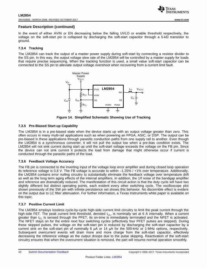
Typical Application (continued)8.2.2.6 Enable and UVLOUsing a resistor divider from VIN to EN as shown in the schematic diagram below, the input voltage at which thepart begins switching can be increased above the normal input UVLO level as shown in Equation 10.
(10)
For example, suppose that the required input UVLO level is 3.69 V. Choosing REN2 = 10 kΩ, then we calculateREN1 = 20 kΩ.
Figure 19. Simplified Schematic Showing Use of EN as an Input UVLO
Alternatively, the EN pin can be driven from another voltage source to cater for system sequencing requirementscommonly found in FPGA and other multi-rail applications. The following schematic shows an LM2854 that issequenced to start based on the voltage level of a master system rail.
Figure 20. Simplified Schematic Showing EN Used to Cascade Power Supply Start-up
8.2.2.7 Output Voltage SettingA divider resistor network from VOUT to the FB pin determines the desired output voltage as shown inEquation 11.
(11)
RFB1 is defined based on the voltage loop requirements and RFB2 is then selected for the desired output voltage.These resistors are normally selected as 0.5% or 1% tolerance.
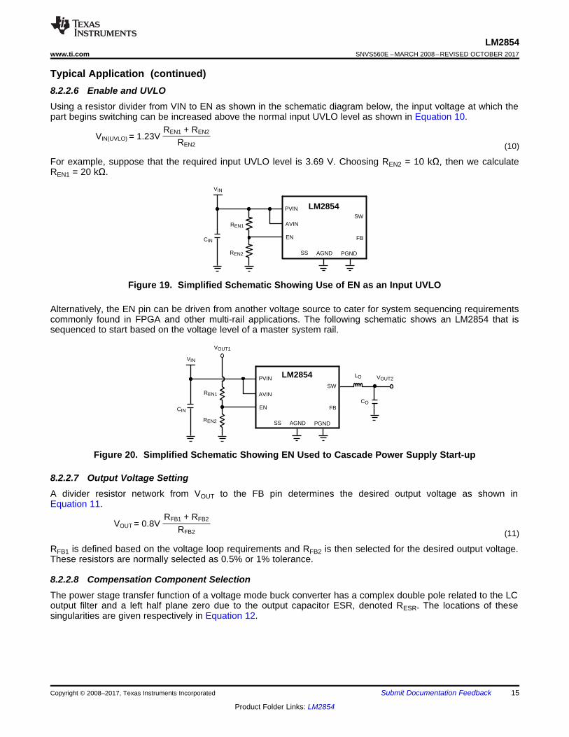
8.2.2.8 Compensation Component SelectionThe power stage transfer function of a voltage mode buck converter has a complex double pole related to the LCoutput filter and a left half plane zero due to the output capacitor ESR, denoted RESR. The locations of thesesingularities are given respectively in Equation 12.
CCOMP(pF) = DLO(PH)CO(PF)
VIN (V)floop (kHz)
PVIN
AVIN
EN
AGND PGND
FB
SW
LM2854 VOUT
SS
LO
CO
RFB1
RCOMP CCOMP
RFB2
VIN
+-
+-
ErrorAmp VREF
PWMComp
Ramp
RDCR
RESR
RL
1
RESR + RLLOCO
fLC =
2SRDCR + RL
LOCO2S
1
fESR = 1
2SRESRCO
#
16
LM2854SNVS560E –MARCH 2008–REVISED OCTOBER 2017 www.ti.com
Product Folder Links: LM2854
Submit Documentation Feedback Copyright © 2008–2017, Texas Instruments Incorporated
Typical Application (continued)
where• CO is the output capacitance value appropriately derated for applied voltage and operating temperature• RL is the effective load resistance• RDCR is the series damping resistance associated with the inductor and power switches (12)
Figure 21. LM2854 Compensation Scheme
The conventional compensation strategy employed with voltage mode control is to use two compensator zeros tooffset the LC double pole, one compensator pole located to cancel the output capacitor ESR zero and onecompensator pole located between one third and one half switching frequency for high frequency noiseattenuation.
The LM2854 internal compensation components are designed to locate a pole at the origin and a pole at highfrequency as mentioned above. Furthermore, a zero is located at 8.8 kHz or 17.6 kHz for the 500 kHz or 1 MHzoptions, respectively, to approximately cancel the likely location of one LC filter pole.
The three external compensation components, RFB1, RCOMP and CCOMP, are selected to position a zero at orbelow the LC pole location and a pole to cancel the ESR zero. The voltage loop crossover frequency, floop, isusually selected between one tenth to one fifth of the switching frequency, as shown in Equation 13.
0.1fSW ≤ floop ≤ 0.2fSW (13)
A simple solution for the required external compensation capacitor, CCOMP, with type III voltage mode control canbe expressed as in Equation 14.
(14)
where the constant α is nominally 0.038 or 0.075 for the 500 kHz or 1 MHz options, respectively. This assumes acompensator pole cancels the output capacitor ESR zero. Furthermore, since the modulator gain is proportionalto VIN, the loop crossover frequency increases with VIN. Thus, it is recommended to design the loop at maximumexpected VIN.
The upper feedback resistor, RFB1, is selected to provide adequate mid-band gain and to locate a zero at orbelow the LC pole frequency. The series resistor, RCOMP, is selected to locate a pole at the ESR zero frequency,as shown in Equation 15.

'iL
'VOUT = 'iL
12ICout(RMS) =
1RESR
2 +8fSWCO
2
LO ='iLfSW
VOUT(1-D)
0.3IOUTfSW
#VOUT(1-D)
RFB1 =2SCCOMPfLC
1
RCOMP =2SCCOMPfESR
1
17
LM2854www.ti.com SNVS560E –MARCH 2008–REVISED OCTOBER 2017
Product Folder Links: LM2854
Submit Documentation FeedbackCopyright © 2008–2017, Texas Instruments Incorporated
Typical Application (continued)
(15)
Note that the lower feedback resistor, RFB2, has no impact on the control loop from an AC standpoint since theFB pin is the input to an error amplifier and effectively at AC ground. Hence, the control loop can be designedirrespective of output voltage level. The only caveat here is the necessary derating of the output capacitance withapplied voltage. Having chosen RFB1 as above, RFB2 is then selected for the desired output voltage.
Table 1 and Table 2 list inductor and ranges of capacitor values that work well with the LM2854, along with theassociated compensation components to ensure stable operation. Values different than those listed may beused, but the compensation components may need to be recalculated to avoid degradation in phase margin.Note that the capacitance ranges specified refer to in-circuit values where the nominal capacitance value isadequately derated for applied voltage.
8.2.2.9 Filter Inductor and Output Capacitor SelectionIn a buck regulator, selection of the filter inductor and capacitor will affect many key system parameters,including stability, transient response and efficiency The LM2854 can accommodate relatively wide ranges ofoutput capacitor and filter inductor values in a typical application and still achieve excellent load current transientperformance and low output voltage ripple.
The inductance is chosen such that the peak-to-peak inductor current ripple, ΔiL, is approximately 25 to 40% ofIOUT as shown in Equation 16.
(16)
Note that the peak inductor current is the DC output current plus half the ripple current and reaches its highestlevel at lowest duty cycle (or highest VIN). It is recommended that the inductor should have a saturation currentrating in excess of the current limit level.
When operating the LM2854 at input voltages above 5.2 V, the inductor should be sized to keep the minimuminductor current above –0.5 A. For most applications this should only occur at light loads or when the inductor isdrastically undersized. To ensure the current never goes below –0.5 A for any application, the peak-to-peakripple current (ΔiL) in the inductor should be less than 1 A. Keeping the minimum inductor current above –0.5 Alimits the energy storage in the inductor and helps prevent the switch node voltage from exceeding the absolutemaximum specification when the low side FET turns off.
Table 3 lists examples of off-the-shelf powdered iron and ferrite based inductors that are suitable for use with theLM2854. The output capacitor can be of ceramic or electrolytic chemistry. The chosen output capacitor requiressufficient DC voltage rating and RMS ripple current handling capability.
The output capacitor RMS current and peak-to-peak output ripple are given respectively as in Equation 17.
(17)
In general, 22 µF to 100 µF of ceramic output capacitance is sufficient for both LM2854 frequency options giventhe optimal high frequency characteristics and low ESR of ceramic dielectric. It is advisable to consult themanufacturer’s derating curves for capacitance voltage coefficient as the in-circuit capacitance may dropsignificantly with applied voltage.

18
LM2854SNVS560E –MARCH 2008–REVISED OCTOBER 2017 www.ti.com
Product Folder Links: LM2854
Submit Documentation Feedback Copyright © 2008–2017, Texas Instruments Incorporated
Typical Application (continued)Tantalum or organic polymer electrolytic capacitance may be suitable with the LM2854 500 kHz option,particularly in applications where substantial bulk capacitance per unit volume is required. However, the highloop bandwidth achievable with the LM2854 obviates the necessity for large bulk capacitance during transientloading conditions.
Table 4 lists some examples of commercially available capacitors that can be used with the LM2854.
Table 1. LM2854 500-kHz Compensation Component Values
VIN (V) LO (µH)CO (µF) ESR (mΩ)
RFB1 (kΩ) CCOMP (pF) RCOMP (kΩ)MIN MAX MIN MAX
5
1.5 40 100 2 10 150 47 11.5 100 200 1 5 150 100 11.5 100 220 15 25 150 120 252.2 40 100 2 10 150 68 12.2 100 200 1 5 150 120 12.2 100 220 15 25 120 120 15
3.3
1.5 40 100 2 10 150 68 11.5 100 200 1 5 100 150 11.5 100 220 15 25 100 150 152.2 40 100 2 10 150 100 12.2 100 200 1 5 100 220 12.2 100 220 15 25 100 220 10
Table 2. LM2854 1-MHz Compensation Component Values
VIN (V) LO (µH)CO (µF) ESR (mΩ)
RFB1 (kΩ) CCOMP (pF) RCOMP (kΩ)MIN MAX MIN MAX
5
0.68 20 60 2 10 120 33 10.68 60 150 1 5 75 100 10.68 100 220 15 25 100 100 20
1 20 60 2 10 100 56 11 60 150 1 5 75 150 11 100 220 15 25 75 150 15
3.3
0.68 20 60 2 10 75 56 10.68 60 150 1 5 50 150 10.68 100 220 15 25 50 150 12
1 20 60 2 10 75 82 11 60 150 1 5 50 220 11 100 220 15 25 33 330 10
Table 3. Recommended Filter InductorsINDUCTANCE (µH) DCR (mΩ) MANUFACTURER MANUFACTURER P/N CASE SIZE (mm)
0.47 14.5 Vishay Dale IHLP1616BZERR47M11 4.06 × 4.45 × 2.001 24 Vishay Dale IHLP1616BZER1R0M11 4.06 × 4.45 × 2.00
0.47 8.4 Vishay Dale IHLP2525AHERR47M01 6.47 × 6.86 × 1.800.47 6 Vishay Dale IHLP2525BDERR47M01 6.47 × 6.86 × 2.400.68 8.7 Vishay Dale IHLP2525BDERR68M01 6.47 × 6.86 × 2.400.82 10.6 Vishay Dale IHLP2525BDERR82M01 6.47 × 6.86 × 2.40
1 13.1 Vishay Dale IHLP2525BDER1R0M01 6.47 × 6.86 × 2.401.5 18.5 Vishay Dale IHLP2525BDER1R5M01 6.47 × 6.86 × 2.40

19
LM2854www.ti.com SNVS560E –MARCH 2008–REVISED OCTOBER 2017
Product Folder Links: LM2854
Submit Documentation FeedbackCopyright © 2008–2017, Texas Instruments Incorporated
Table 3. Recommended Filter Inductors (continued)INDUCTANCE (µH) DCR (mΩ) MANUFACTURER MANUFACTURER P/N CASE SIZE (mm)
2.2 15.7 Vishay Dale IHLP2525CZER2R2M11 6.47 × 6.86 × 3.000.47 3.5 Sumida CDMC6D28NP-R47M 6.50 × 7.25 × 3.000.68 4.5 Sumida CDMC6D28NP-R68M 6.50 × 7.25 × 3.00
1 17.3 Sumida CDMC6D28NP-1R0M 6.50 × 7.25 × 3.001.5 10.4 Sumida CDMC6D28NP-1R5M 6.50 × 7.25 × 3.002.2 16.1 Sumida CDMC6D28NP-2R2M 6.50 × 7.25 × 3.000.56 10 Coilcraft DO1813H-561ML 6.10 × 8.89 × 5.000.47 3.3 Coilcraft HA3619-471ALC 7 × 7 × 30.68 4.8 Coilcraft HA3619-681ALC 7 × 7 × 3
1 7.5 Coilcraft HA3619-102ALC 7 × 7 × 31.2 9.4 Coilcraft HA3619-122ALC 7 × 7 × 31.5 11.5 Coilcraft HA3619-152ALC 7 × 7 × 31.8 16.5 Coilcraft HA3619-182ALC 7 × 7 × 30.47 3.3 TDK SPM6530T-R47M170 7.1 × 6.5 × 30.68 4.9 TDK SPM6530T-R68M140 7.1 × 6.5 × 3
1 7.1 TDK SPM6530T-1R0M120 7.1 × 6.5 × 31.5 9.7 TDK SPM6530T-1R5M100 7.1 × 6.5 × 30.47 14 Cyntec PCMC042T-0R47MN 4 × 4.5 × 21.0 9 Cyntec PCMC063T-1R0MN 6.5 × 6.9 × 31.5 14 Cyntec PCMC063T-1R5MN 6.5 × 6.9 × 3
Table 4. Recommended Filter CapacitorsCAPACITANCE
(µF)VOLTAGE (V), ESR
(mΩ) CHEMISTRY MANUFACTURER MANUFACTURER P/N CASE SIZE
22 6.3, < 5 Ceramic, X5R TDK C3216X5R0J226M 120647 6.3, < 5 Ceramic, X5R TDK C3216X5R0J476M 120647 6.3, < 5 Ceramic, X5R TDK C3225X5R0J476M 121047 10, < 5 Ceramic, X5R TDK C3225X5R1A476M 1210100 6.3, < 5 Ceramic, X5R TDK C3225X5R0J107M 1210100 6.3, 50 Tantalum AVX TPSD157M006#0050 D, 7.5 × 4.3 × 2.9 mm100 6.3, 25 Organic Polymer Sanyo 6TPE100MPB2 B2, 3.5 × 2.8 × 1.9 mm150 6.3, 18 Organic Polymer Sanyo 6TPE150MIC2 C2, 6 × 3.2 × 1.8 mm
330 6.3, 18 Organic Polymer Sanyo 6TPE330MIL D3L, 7.3 × 4.3 × 2.8mm
470 6.3, 23 Niobium Oxide AVX NOME37M006#0023 E, 7.3 × 4.3 × 4.1 mm

0 484
86
88
90
92
94
96
EF
FIC
IEN
CY
(%
)
LOAD CURRENT (A)
1 2 3
VIN = 3.3V
VIN = 5.0V
0 476
94
EF
FIC
IEN
CY
(%
)
LOAD CURRENT (A)
1 2 3
78
80
82
84
86
88
90
92
VIN = 3.3V
VIN = 5.0V
0 480
82
84
86
88
90
92
94
EF
FIC
IEN
CY
(%
)
LOAD CURRENT (A)
1 2 3
VIN = 3.3V
VIN = 5.0V
0 492
93
94
95
96
97
98
EF
FIC
IEN
CY
(%
)
LOAD CURRENT (A)
1 2 3
VIN = 4.0V
VIN = 5.0V
0 474
92
EF
FIC
IEN
CY
(%
)
LOAD CURRENT (A)
1 2 3
76
78
80
82
84
86
88
90 VIN = 3.3V
VIN = 5.0V
0 489
90
91
92
93
94
95
96
97
EF
FIC
IEN
CY
(%
)
LOAD CURRENT (A)
1 2 3
VIN = 3.3V
VIN = 5.0V
20
LM2854SNVS560E –MARCH 2008–REVISED OCTOBER 2017 www.ti.com
Product Folder Links: LM2854
Submit Documentation Feedback Copyright © 2008–2017, Texas Instruments Incorporated
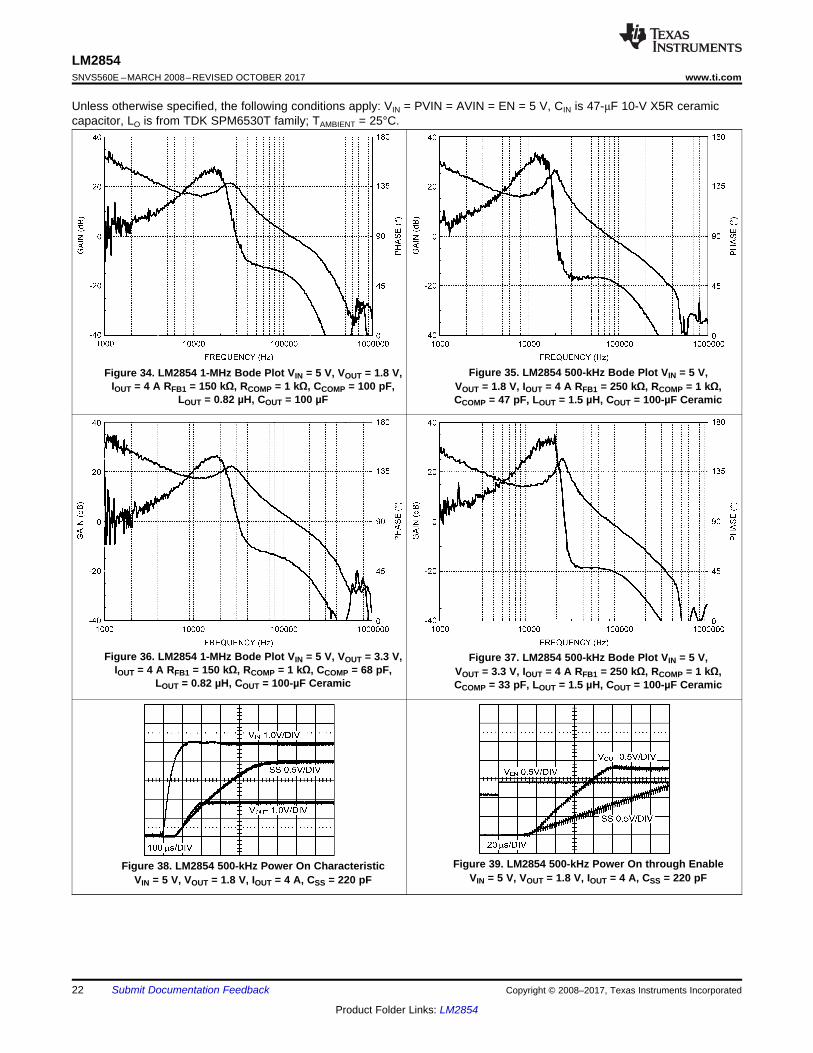
8.2.3 Application CurvesUnless otherwise specified, the following conditions apply: VIN = PVIN = AVIN = EN = 5 V, CIN is 47-μF 10-V X5R ceramiccapacitor, LO is from TDK SPM6530T family; TAMBIENT = 25°C.
Figure 22. LM2854 1-MHz Efficiency vs IOUT VOUT = 0.8 V,LO = 0.47 µH, 3.3-mΩ DCR
Figure 23. LM2854 1-MHz Efficiency vs IOUT VOUT = 2.5 V,LO = 1 µH, 7.1-mΩ DCR
Figure 24. LM2854 1-MHz Efficiency vs IOUT VOUT = 1.2 V,LO = 0.68 µH, 4.9-mΩ DCR
Figure 25. LM2854 1-MHz Efficiency vs IOUT VOUT = 3.3 V,LO = 1 µH, 7.1-mΩ DCR
Figure 26. LM2854 1-MHz Efficiency vs IOUT VOUT = 1.8 V,LO = 1 µH, 7.1-mΩ DCR
Figure 27. LM2854 500-kHz Efficiency vs IOUT VOUT = 0.8 V,LO = 1 µH, 7.1-mΩ DCR

0 492
93
94
95
96
97
98
99
EF
FIC
IEN
CY
(%
)
LOAD CURRENT (A)
1 2 3
VIN = 5.0V
VIN = 4.0V
0 484
86
88
90
92
94
96
98
EF
FIC
IEN
CY
(%
)
LOAD CURRENT (A)
1 2 3
VIN = 5.0V
VIN = 3.3V
0 490
99E
FF
ICIE
NC
Y (
%)
LOAD CURRENT (A)
1 2 3
91
92
93
94
95
96
97
98
VIN = 3.3V
VIN = 5.0V
0 480
82
84
86
88
90
92
94
96
EF
FIC
IEN
CY
(%
)
LOAD CURRENT (A)
1 2 3
VIN = 3.3V
VIN = 5.0V
21
LM2854www.ti.com SNVS560E –MARCH 2008–REVISED OCTOBER 2017
Product Folder Links: LM2854
Submit Documentation FeedbackCopyright © 2008–2017, Texas Instruments Incorporated
Unless otherwise specified, the following conditions apply: VIN = PVIN = AVIN = EN = 5 V, CIN is 47-μF 10-V X5R ceramiccapacitor, LO is from TDK SPM6530T family; TAMBIENT = 25°C.
Figure 28. LM2854 500-kHz Efficiency vs IOUT VOUT = 2.5 V,LO = 2.2 µH, 16-mΩ DCR
Figure 29. LM2854 500-kHz Efficiency vs IOUT VOUT = 1.2 V,LO = 1.5 µH, 9.7-mΩ DCR
Figure 30. LM2854 500-kHz Efficiency vs IOUT VOUT = 3.3 V,LO = 1.5 µH, 9.7-mΩ DCR
Figure 31. LM2854 500-kHz Efficiency vs IOUT VOUT = 1.8 V,LO = 1.5 µH, 9.7-mΩ DCR
Figure 32. LM2854 1-MHz Bode Plot VIN = 3.3 V, VOUT = 1.8V, IOUT = 4 A RFB1 = 150 kΩ, RCOMP = 1 kΩ, CCOMP = 100 pF,
LOUT = 0.82 µH, COUT = 100-µF Ceramic
Figure 33. LM2854 500-kHz Bode Plot VIN = 3.3 V,VOUT = 1.8 V, IOUT = 4 A RFB1 = 250 kΩ, RCOMP = 1 kΩ,CCOMP = 47 pF, LOUT = 1.5 µH, COUT = 100-µF Ceramic
22
LM2854SNVS560E –MARCH 2008–REVISED OCTOBER 2017 www.ti.com
Product Folder Links: LM2854
Submit Documentation Feedback Copyright © 2008–2017, Texas Instruments Incorporated
Unless otherwise specified, the following conditions apply: VIN = PVIN = AVIN = EN = 5 V, CIN is 47-μF 10-V X5R ceramiccapacitor, LO is from TDK SPM6530T family; TAMBIENT = 25°C.
Figure 34. LM2854 1-MHz Bode Plot VIN = 5 V, VOUT = 1.8 V,IOUT = 4 A RFB1 = 150 kΩ, RCOMP = 1 kΩ, CCOMP = 100 pF,
LOUT = 0.82 µH, COUT = 100 µF
Figure 35. LM2854 500-kHz Bode Plot VIN = 5 V,VOUT = 1.8 V, IOUT = 4 A RFB1 = 250 kΩ, RCOMP = 1 kΩ,CCOMP = 47 pF, LOUT = 1.5 µH, COUT = 100-µF Ceramic
Figure 36. LM2854 1-MHz Bode Plot VIN = 5 V, VOUT = 3.3 V,IOUT = 4 A RFB1 = 150 kΩ, RCOMP = 1 kΩ, CCOMP = 68 pF,
LOUT = 0.82 µH, COUT = 100-µF Ceramic
Figure 37. LM2854 500-kHz Bode Plot VIN = 5 V,VOUT = 3.3 V, IOUT = 4 A RFB1 = 250 kΩ, RCOMP = 1 kΩ,CCOMP = 33 pF, LOUT = 1.5 µH, COUT = 100-µF Ceramic
Figure 38. LM2854 500-kHz Power On CharacteristicVIN = 5 V, VOUT = 1.8 V, IOUT = 4 A, CSS = 220 pF
Figure 39. LM2854 500-kHz Power On through EnableVIN = 5 V, VOUT = 1.8 V, IOUT = 4 A, CSS = 220 pF
PVIN
AVIN
EN
AGND PGND
FB
SWLM2854
VIN
VOUT
SS
CIN
LO
CO
RFB1
RCOMP CCOMPRFB2
CSS
CF
RF
U1
23
LM2854www.ti.com SNVS560E –MARCH 2008–REVISED OCTOBER 2017
Product Folder Links: LM2854
Submit Documentation FeedbackCopyright © 2008–2017, Texas Instruments Incorporated
Unless otherwise specified, the following conditions apply: VIN = PVIN = AVIN = EN = 5 V, CIN is 47-μF 10-V X5R ceramiccapacitor, LO is from TDK SPM6530T family; TAMBIENT = 25°C.
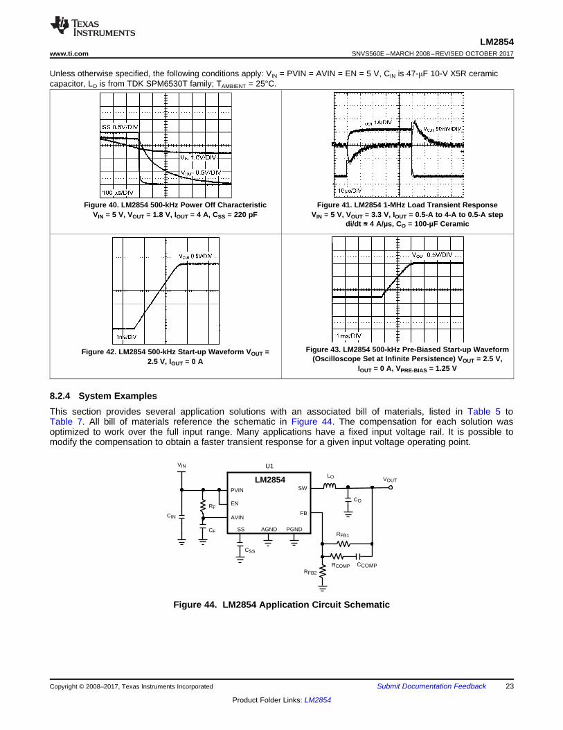
Figure 40. LM2854 500-kHz Power Off CharacteristicVIN = 5 V, VOUT = 1.8 V, IOUT = 4 A, CSS = 220 pF
Figure 41. LM2854 1-MHz Load Transient ResponseVIN = 5 V, VOUT = 3.3 V, IOUT = 0.5-A to 4-A to 0.5-A step
di/dt ≊≊ 4 A/µs, CO = 100-µF Ceramic
Figure 42. LM2854 500-kHz Start-up Waveform VOUT =2.5 V, IOUT = 0 A
Figure 43. LM2854 500-kHz Pre-Biased Start-up Waveform(Oscilloscope Set at Infinite Persistence) VOUT = 2.5 V,
IOUT = 0 A, VPRE-BIAS = 1.25 V
8.2.4 System ExamplesThis section provides several application solutions with an associated bill of materials, listed in Table 5 toTable 7. All bill of materials reference the schematic in Figure 44. The compensation for each solution wasoptimized to work over the full input range. Many applications have a fixed input voltage rail. It is possible tomodify the compensation to obtain a faster transient response for a given input voltage operating point.
Figure 44. LM2854 Application Circuit Schematic

24
LM2854SNVS560E –MARCH 2008–REVISED OCTOBER 2017 www.ti.com
Product Folder Links: LM2854
Submit Documentation Feedback Copyright © 2008–2017, Texas Instruments Incorporated
Unless otherwise specified, the following conditions apply: VIN = PVIN = AVIN = EN = 5 V, CIN is 47-μF 10-V X5R ceramiccapacitor, LO is from TDK SPM6530T family; TAMBIENT = 25°C.
Table 5. LM2854 500-kHz Bill of Materials, VIN = 5 V, VOUT = 3.3 V, IOUT(MAX) = 4 A, Optimized forEfficiency
REF DES DESCRIPTION CASE SIZE MANUFACTURER MANUFACTURER P/N
U1 Synchronous BuckRegulator HTSSOP-16 Texas Instruments LM2854MHX-500
CIN 47 µF, X5R, 10 V 1210 TDK C3225X5R1A476MCO 100 µF, X5R, 6.3 V 1210 TDK C3225X5R0J107MLO 1.5 µH, 9.7 mΩ, 10 A 7.1 × 6.5 × 3.0 mm TDK SPM6530T-1R5M100
RFB1 249 kΩ 0603 Vishay Dale CRCW06032493F-e3RFB2 80.6 kΩ 0603 Vishay Dale CRCW060328062F-e3
RCOMP 1 kΩ 0603 Vishay Dale CRCW06031001F-e3RF 1 Ω 0603 Vishay Dale CRCW06031R0F-e3
CCOMP 33 pF, ±5%, C0G, 50 V 0603 TDK C1608C0G1H330JCSS 10 nF, ±10%, X7R, 16 V 0603 Murata GRM188R71C103KA01CF 1.0 µF, ±10%, X7R, 10 V 0603 Murata GRM188R71A105KA61
Table 6. LM2854 1-MHz Bill of Materials, VIN = 3.3 V to 5 V, VOUT = 2.5 V, IOUT (MAX) = 4 A, Optimized forElectrolytic Input and Output Capacitance
REF DES DESCRIPTION CASE SIZE MANUFACTURER MANUFACTURER P/NU1 Synchronous Buck Regulator HTSSOP-16 Texas Instruments LM2854MHX-1000CIN 150 µF, 6.3 V, 18 mΩ C2, 6 × 3.2 × 1.8 mm Sanyo 6TPE150MIC2CO 330 µF, 6.3 V, 18 mΩ D3L, 7.3 × 4.3 × 2.8 mm Sanyo 6TPE330MILLO 2.2 µH, 16 mΩ, 7 A 6.47 × 6.86 × 3 mm Vishay Dale IHLP2525CZER2R2M11
RFB1 100 kΩ 0603 Vishay Dale CRCW06031003F-e3RFB2 47.5 kΩ 0603 Vishay Dale CRCW060324752F-e3
RCOMP 15 kΩ 0603 Vishay Dale CRCW06031502F-e3RF 1 Ω 0603 Vishay Dale CRCW06031R0F-e3
CCOMP 330 pF, ±5%, C0G, 50 V 0603 TDK C1608C0G1H331JCSS 10 nF, ±10%, X7R, 16 V 0603 Murata GRM188R71C103KA01CF 1 µF,±10%, X7R, 10 V 0603 Murata GRM188R71A105KA61
Table 7. LM2854 1-MHz Bill of Materials, VIN = 3.3 V, VOUT = 0.8 V, IOUT (MAX) = 4 A, Optimized for SolutionSize and Transient Response
REF DES DESCRIPTION CASE SIZE MANUFACTURER MANUFACTURER P/NU1 Synchronous Buck Regulator HTSSOP-16 Texas Instruments LM2854MHX-1000CIN 47 µF, X5R, 6.3 V 1206 TDK C3216X5R0J476MCO 47 µF, X5R, 6.3 V 1206 TDK C3216X5R0J476MLO 0.47 µH, 14.5 mΩ, 7 A 4.06 × 4.45 × 2.00 mm Vishay Dale IHLP1616BZER0R47M11
RFB1 110 kΩ 0402 Vishay Dale CRCW04021103F-e3RCOMP 1 kΩ 0402 Vishay Dale CRCW04021001F-e3
RF 1 Ω 0402 Vishay Dale CRCW04021R0F-e3CCOMP 27 pF, ±5%, C0G, 50 V 0402 Murata GRM1555C1H270JZ01
CSS 10 nF, ±10%, X7R, 16 V 0402 Murata GRM155R71C103KA01CF 1 µF, ±10%, X7R, 10 V 0402 Murata GRM155R61A105KE15

25
LM2854www.ti.com SNVS560E –MARCH 2008–REVISED OCTOBER 2017
Product Folder Links: LM2854
Submit Documentation FeedbackCopyright © 2008–2017, Texas Instruments Incorporated
9 Power Supply RecommendationsThe LM2854 is designed to operate from an input voltage supply range from 2.95 V to 5.5 V. This input supplyshould be able to source the maximum input current and maintain a voltage above either 2.95 V or the outputvoltage, whichever is higher. In cases where input supply is located at a distance (more than a few inches) fromthe device, drop due to traces and wires must be considered.
10 Layout
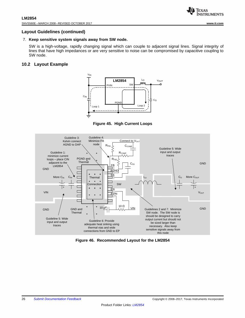
10.1 Layout GuidelinesPC board layout is an important part of DC-DC converter design. Poor board layout can disrupt the performanceof a DC-DC converter and surrounding circuitry by contributing to EMI, ground bounce and resistive voltage dropin the traces. These can send erroneous signals to the DC-DC converter resulting in poor regulation or instability.Good layout can be implemented by following a few simple design rules.1. Minimize area of switched current loops.
There are two loops where currents are switched at high di/dt slew rates in a buck regulator. The first looprepresents the path taken by AC current flowing during the high side PFET on time. This current flows fromthe input capacitor to the regulator PVIN pins, through the high side FET to the regulator SW pin, filterinductor, output capacitor and returning via the PCB ground plane to the input capacitor.The second loop represents the path taken by AC current flowing during the low side NFET on time. Thiscurrent flows from the output capacitor ground to the regulator PGND pins, through the NFET to the inductorand output capacitor. From an EMI reduction standpoint, it is imperative to minimize this loop area during PCboard layout by physically locating the input capacitor close to the LM2854. Specifically, it is advantageous toplace CIN as close as possible to the LM2854 PVIN and PGND pins. Grounding for both the input and outputcapacitor should consist of a localized top side plane that connects to PGND and the exposed die attach pad(DAP). The inductor should be placed close to the SW pin and output capacitor.
2. Minimize the copper area of the switch node.The LM2854 has two SW pins optimally located on one side of the package. In general the SW pins shouldbe connected to the filter inductor on the top PCB layer. The inductor should be placed close to the SW pinsto minimize the copper area of the switch node.
3. Have a single point ground for all device analog grounds located under the DAP.The ground connections for the Feedback, Soft-start, Enable and AVIN components should be routed to theAGND pin of the device. The AGND pin should connect to PGND under the DAP. This prevents anyswitched or load currents from flowing in the analog ground traces. If not properly handled, poor groundingcan result in degraded load regulation or erratic switching behavior.
4. Minimize trace length to the FB pin.Since the feedback (FB) node is high impedance, the trace from the output voltage setpoint resistor divider toFB pin should be as short as possible. This is most important as relatively high value resistors are used toset the output voltage. The FB trace should be routed away from the SW pin and inductor to avoid noisepickup from the SW pin. Both feedback resistors, RFB1 and RFB2, and the compensation components, RCOMPand CCOMP, should be located close to the FB pin.
5. Make input and output bus connections as wide as possible.This reduces any voltage drops on the input or output of the converter and maximizes efficiency. To optimizevoltage accuracy at the load, ensure that a separate feedback voltage sense trace is made to the load. Doingso will correct for voltage drops and provide optimum output accuracy.
6. Provide adequate device heat-sinking.Use an array of heat-sinking vias to connect the DAP to the ground plane on the bottom PCB layer. If thePCB has a plurality of copper layers, these thermal vias can also be employed to make connection to innerlayer heat-spreading ground planes. For best results use a 5 x 3 via array with minimum via diameter of 10mils. Ensure enough copper area is used to keep the junction temperature below 125°C.
CIN
RFB1
CO
RFB2
CCOMP
More CIN
+
More COUT
+
CSSFB
AGND
SS
SW
PGND and Thermal
VIN VOUT
GND and Thermal
10 F
RCOMP
EN
AVIN
GND
GND
GND
GND
Connect to VOUT
Thermal
Connection
10 VIN
LO
Guideline 1: minimize current
loops ± place CIN adjacent to the
LM2854
Guideline 3: Kelvin connect AGND to DAP
Guidelines 2 and 7: Minimize SW node. The SW node is should be designed to carry output current but should not
be sized larger than necessary. Also keep
sensitive signals away from this node
Guideline 4: Minimize FB
node
Guideline 5: Wide input and output
traces
Guideline 5: Wide input and output
traces
Guideline 6: Provide adequate heat sinking using
thermal vias and wide connections from GND to EP
PVIN
PGND
SW
LM2854
VIN
VOUT
CIN
LO
CO
Loop 1 Loop 2
26
LM2854SNVS560E –MARCH 2008–REVISED OCTOBER 2017 www.ti.com
Product Folder Links: LM2854
Submit Documentation Feedback Copyright © 2008–2017, Texas Instruments Incorporated
Layout Guidelines (continued)7. Keep sensitive system signals away from SW node.
SW is a high-voltage, rapidly changing signal which can couple to adjacent signal lines. Signal integrity oflines that have high impedances or are very sensitive to noise can be compromised by capacitive coupling toSW node.
10.2 Layout Example
Figure 45. High Current Loops
Figure 46. Recommended Layout for the LM2854

27
LM2854www.ti.com SNVS560E –MARCH 2008–REVISED OCTOBER 2017
Product Folder Links: LM2854
Submit Documentation FeedbackCopyright © 2008–2017, Texas Instruments Incorporated
11 Device and Documentation Support
11.1 Documentation Support
11.1.1 Related DocumentationFor related documentation, see the following:• AN-1786 LM2854 500 kHz Buck Regulator Evaluation Board (Rev. B), SNVA323• AN-1880 LM2854 1MHz Buck Regulator Demo Board (Rev. B), SNVA358• AN-1149 Layout Guidelines for Switching Power Supplies, SNVA021• AN-1229 PCB Layout Guidelines, SNVA054• Constructing Your Power Supply- Layout Considerations, SLUP230• Low Radiated EMI Layout Made SIMPLE with LM4360x and LM4600x, SNVA721• AN-2020 Thermal Design By Insight, Not Hindsight, SNVA419• AN-1520 A Guide to Board Layout for Best Thermal Resistance for Exposed Pad Packages, SNVA183• Semiconductor and IC Package Thermal Metrics, SPRA953• Thermal Design made Simple with LM43603 and LM43602, SNVA719• Using New Thermal Metrics, SBVA025
11.2 TrademarksPowerWise is a trademark of Texas Instrumetns, Inc.All other trademarks are the property of their respective owners.
11.3 Electrostatic Discharge CautionThese devices have limited built-in ESD protection. The leads should be shorted together or the device placed in conductive foamduring storage or handling to prevent electrostatic damage to the MOS gates.
11.4 GlossarySLYZ022 — TI Glossary.
This glossary lists and explains terms, acronyms, and definitions.
12 Mechanical, Packaging, and Orderable InformationThe following pages include mechanical, packaging, and orderable information. This information is the mostcurrent data available for the designated devices. This data is subject to change without notice and revision ofthis document. For browser-based versions of this data sheet, refer to the left-hand navigation.

PACKAGE OPTION ADDENDUM
www.ti.com 4-Oct-2017
Addendum-Page 1
PACKAGING INFORMATION
Orderable Device Status(1)
Package Type PackageDrawing
Pins PackageQty
Eco Plan(2)
Lead/Ball Finish(6)
MSL Peak Temp(3)
Op Temp (°C) Device Marking(4/5)
Samples
LM2854MH-1000 NRND HTSSOP PWP 16 92 TBD Call TI Call TI -40 to 85 LM2854-1000
LM2854MH-1000/NOPB ACTIVE HTSSOP PWP 16 92 Green (RoHS& no Sb/Br)
CU SN Level-1-260C-UNLIM -40 to 85 LM2854-1000
LM2854MH-500/NOPB ACTIVE HTSSOP PWP 16 92 Green (RoHS& no Sb/Br)
CU SN Level-1-260C-UNLIM -40 to 85 LM2854-500
LM2854MHX-1000/NOPB ACTIVE HTSSOP PWP 16 2500 Green (RoHS& no Sb/Br)
CU SN Level-1-260C-UNLIM -40 to 85 LM2854-1000
LM2854MHX-500/NOPB ACTIVE HTSSOP PWP 16 2500 Green (RoHS& no Sb/Br)
CU SN Level-1-260C-UNLIM -40 to 85 LM2854-500
(1) The marketing status values are defined as follows:ACTIVE: Product device recommended for new designs.LIFEBUY: TI has announced that the device will be discontinued, and a lifetime-buy period is in effect.NRND: Not recommended for new designs. Device is in production to support existing customers, but TI does not recommend using this part in a new design.PREVIEW: Device has been announced but is not in production. Samples may or may not be available.OBSOLETE: TI has discontinued the production of the device.
(2) RoHS: TI defines "RoHS" to mean semiconductor products that are compliant with the current EU RoHS requirements for all 10 RoHS substances, including the requirement that RoHS substancedo not exceed 0.1% by weight in homogeneous materials. Where designed to be soldered at high temperatures, "RoHS" products are suitable for use in specified lead-free processes. TI mayreference these types of products as "Pb-Free".RoHS Exempt: TI defines "RoHS Exempt" to mean products that contain lead but are compliant with EU RoHS pursuant to a specific EU RoHS exemption.Green: TI defines "Green" to mean the content of Chlorine (Cl) and Bromine (Br) based flame retardants meet JS709B low halogen requirements of <=1000ppm threshold. Antimony trioxide basedflame retardants must also meet the <=1000ppm threshold requirement.
(3) MSL, Peak Temp. - The Moisture Sensitivity Level rating according to the JEDEC industry standard classifications, and peak solder temperature.
(4) There may be additional marking, which relates to the logo, the lot trace code information, or the environmental category on the device.
(5) Multiple Device Markings will be inside parentheses. Only one Device Marking contained in parentheses and separated by a "~" will appear on a device. If a line is indented then it is a continuationof the previous line and the two combined represent the entire Device Marking for that device.
(6) Lead/Ball Finish - Orderable Devices may have multiple material finish options. Finish options are separated by a vertical ruled line. Lead/Ball Finish values may wrap to two lines if the finishvalue exceeds the maximum column width.

PACKAGE OPTION ADDENDUM
www.ti.com 4-Oct-2017
Addendum-Page 2
Important Information and Disclaimer:The information provided on this page represents TI's knowledge and belief as of the date that it is provided. TI bases its knowledge and belief on informationprovided by third parties, and makes no representation or warranty as to the accuracy of such information. Efforts are underway to better integrate information from third parties. TI has taken andcontinues to take reasonable steps to provide representative and accurate information but may not have conducted destructive testing or chemical analysis on incoming materials and chemicals.TI and TI suppliers consider certain information to be proprietary, and thus CAS numbers and other limited information may not be available for release.
In no event shall TI's liability arising out of such information exceed the total purchase price of the TI part(s) at issue in this document sold by TI to Customer on an annual basis.
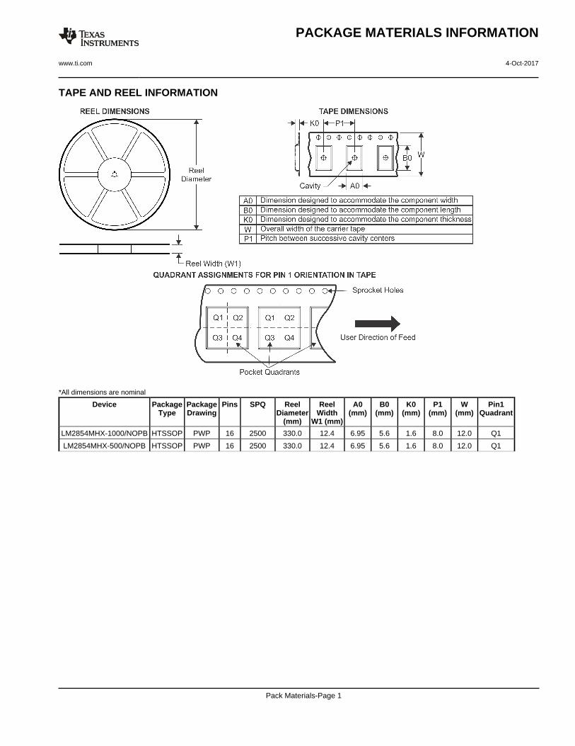
TAPE AND REEL INFORMATION
*All dimensions are nominal
Device PackageType
PackageDrawing
Pins SPQ ReelDiameter
(mm)
ReelWidth
W1 (mm)
A0(mm)
B0(mm)
K0(mm)
P1(mm)
W(mm)
Pin1Quadrant
LM2854MHX-1000/NOPB HTSSOP PWP 16 2500 330.0 12.4 6.95 5.6 1.6 8.0 12.0 Q1
LM2854MHX-500/NOPB HTSSOP PWP 16 2500 330.0 12.4 6.95 5.6 1.6 8.0 12.0 Q1
PACKAGE MATERIALS INFORMATION
www.ti.com 4-Oct-2017
Pack Materials-Page 1

*All dimensions are nominal
Device Package Type Package Drawing Pins SPQ Length (mm) Width (mm) Height (mm)
LM2854MHX-1000/NOPB HTSSOP PWP 16 2500 367.0 367.0 35.0
LM2854MHX-500/NOPB HTSSOP PWP 16 2500 367.0 367.0 35.0
PACKAGE MATERIALS INFORMATION
www.ti.com 4-Oct-2017
Pack Materials-Page 2

www.ti.com
PACKAGE OUTLINE
C
TYP6.66.2
14X 0.65
16X 0.300.19
2X4.55
(0.15) TYP
0 - 80.150.05
3.32.7
3.32.7
2X 1.34 MAXNOTE 5
1.2 MAX
(1)
0.25GAGE PLANE
0.750.50
A
NOTE 3
5.14.9
B 4.54.3
4X 0.166 MAXNOTE 5
4214868/A 02/2017
PowerPAD HTSSOP - 1.2 mm max heightPWP0016APLASTIC SMALL OUTLINE
NOTES: 1. All linear dimensions are in millimeters. Any dimensions in parenthesis are for reference only. Dimensioning and tolerancing per ASME Y14.5M. 2. This drawing is subject to change without notice. 3. This dimension does not include mold flash, protrusions, or gate burrs. Mold flash, protrusions, or gate burrs shall not exceed 0.15 mm per side.4. Reference JEDEC registration MO-153.5. Features may not be present.
PowerPAD is a trademark of Texas Instruments.
TM
116
0.1 C A B
98
PIN 1 IDAREA
SEATING PLANE
0.1 C
SEE DETAIL A
DETAIL ATYPICAL
SCALE 2.400
THERMALPAD
17

www.ti.com
EXAMPLE BOARD LAYOUT
(5.8)
0.05 MAXALL AROUND
0.05 MINALL AROUND
16X (1.5)
16X (0.45)
14X (0.65)
(3.4)NOTE 9
(5)NOTE 9
(3.3)
(3.3)
( 0.2) TYPVIA (1.1) TYP
(1.1)TYP
4214868/A 02/2017
PowerPAD HTSSOP - 1.2 mm max heightPWP0016APLASTIC SMALL OUTLINE
SYMM
SYMM
SEE DETAILS
LAND PATTERN EXAMPLEEXPOSED METAL SHOWN
SCALE:10X
1
8 9
16
METAL COVEREDBY SOLDER MASK
SOLDER MASKDEFINED PAD
17
NOTES: (continued) 6. Publication IPC-7351 may have alternate designs. 7. Solder mask tolerances between and around signal pads can vary based on board fabrication site. 8. This package is designed to be soldered to a thermal pad on the board. For more information, see Texas Instruments literature numbers SLMA002 (www.ti.com/lit/slma002) and SLMA004 (www.ti.com/lit/slma004).9. Size of metal pad may vary due to creepage requirement.
TM
METALSOLDER MASKOPENING
NON SOLDER MASKDEFINED
SOLDER MASK DETAILSPADS 1-16
EXPOSEDMETAL
SOLDER MASKDEFINED
SOLDER MASKMETAL UNDER SOLDER MASK
OPENING
EXPOSEDMETAL

www.ti.com
EXAMPLE STENCIL DESIGN
16X (1.5)
16X (0.45)
(3.3)
(3.3)BASED ON
0.125 THICKSTENCIL
14X (0.65)
(R0.05) TYP
(5.8)
4214868/A 02/2017
PowerPAD HTSSOP - 1.2 mm max heightPWP0016APLASTIC SMALL OUTLINE
2.79 X 2.790.1753.01 X 3.010.15
3.3 X 3.3 (SHOWN)0.1253.69 X 3.690.1
SOLDER STENCILOPENING
STENCILTHICKNESS
NOTES: (continued) 10. Laser cutting apertures with trapezoidal walls and rounded corners may offer better paste release. IPC-7525 may have alternate design recommendations. 11. Board assembly site may have different recommendations for stencil design.
TM
SYMM
SYMM
1
89
16
BASED ON0.125 THICK
STENCIL
BY SOLDER MASKMETAL COVERED
SEE TABLE FORDIFFERENT OPENINGSFOR OTHER STENCILTHICKNESSES
SOLDER PASTE EXAMPLEEXPOSED PAD
100% PRINTED SOLDER COVERAGE BY AREASCALE:10X
17

IMPORTANT NOTICE
Texas Instruments Incorporated (TI) reserves the right to make corrections, enhancements, improvements and other changes to itssemiconductor products and services per JESD46, latest issue, and to discontinue any product or service per JESD48, latest issue. Buyersshould obtain the latest relevant information before placing orders and should verify that such information is current and complete.TI’s published terms of sale for semiconductor products (http://www.ti.com/sc/docs/stdterms.htm) apply to the sale of packaged integratedcircuit products that TI has qualified and released to market. Additional terms may apply to the use or sale of other types of TI products andservices.Reproduction of significant portions of TI information in TI data sheets is permissible only if reproduction is without alteration and isaccompanied by all associated warranties, conditions, limitations, and notices. TI is not responsible or liable for such reproduceddocumentation. Information of third parties may be subject to additional restrictions. Resale of TI products or services with statementsdifferent from or beyond the parameters stated by TI for that product or service voids all express and any implied warranties for theassociated TI product or service and is an unfair and deceptive business practice. TI is not responsible or liable for any such statements.Buyers and others who are developing systems that incorporate TI products (collectively, “Designers”) understand and agree that Designersremain responsible for using their independent analysis, evaluation and judgment in designing their applications and that Designers havefull and exclusive responsibility to assure the safety of Designers' applications and compliance of their applications (and of all TI productsused in or for Designers’ applications) with all applicable regulations, laws and other applicable requirements. Designer represents that, withrespect to their applications, Designer has all the necessary expertise to create and implement safeguards that (1) anticipate dangerousconsequences of failures, (2) monitor failures and their consequences, and (3) lessen the likelihood of failures that might cause harm andtake appropriate actions. Designer agrees that prior to using or distributing any applications that include TI products, Designer willthoroughly test such applications and the functionality of such TI products as used in such applications.TI’s provision of technical, application or other design advice, quality characterization, reliability data or other services or information,including, but not limited to, reference designs and materials relating to evaluation modules, (collectively, “TI Resources”) are intended toassist designers who are developing applications that incorporate TI products; by downloading, accessing or using TI Resources in anyway, Designer (individually or, if Designer is acting on behalf of a company, Designer’s company) agrees to use any particular TI Resourcesolely for this purpose and subject to the terms of this Notice.TI’s provision of TI Resources does not expand or otherwise alter TI’s applicable published warranties or warranty disclaimers for TIproducts, and no additional obligations or liabilities arise from TI providing such TI Resources. TI reserves the right to make corrections,enhancements, improvements and other changes to its TI Resources. TI has not conducted any testing other than that specificallydescribed in the published documentation for a particular TI Resource.Designer is authorized to use, copy and modify any individual TI Resource only in connection with the development of applications thatinclude the TI product(s) identified in such TI Resource. NO OTHER LICENSE, EXPRESS OR IMPLIED, BY ESTOPPEL OR OTHERWISETO ANY OTHER TI INTELLECTUAL PROPERTY RIGHT, AND NO LICENSE TO ANY TECHNOLOGY OR INTELLECTUAL PROPERTYRIGHT OF TI OR ANY THIRD PARTY IS GRANTED HEREIN, including but not limited to any patent right, copyright, mask work right, orother intellectual property right relating to any combination, machine, or process in which TI products or services are used. Informationregarding or referencing third-party products or services does not constitute a license to use such products or services, or a warranty orendorsement thereof. Use of TI Resources may require a license from a third party under the patents or other intellectual property of thethird party, or a license from TI under the patents or other intellectual property of TI.TI RESOURCES ARE PROVIDED “AS IS” AND WITH ALL FAULTS. TI DISCLAIMS ALL OTHER WARRANTIES ORREPRESENTATIONS, EXPRESS OR IMPLIED, REGARDING RESOURCES OR USE THEREOF, INCLUDING BUT NOT LIMITED TOACCURACY OR COMPLETENESS, TITLE, ANY EPIDEMIC FAILURE WARRANTY AND ANY IMPLIED WARRANTIES OFMERCHANTABILITY, FITNESS FOR A PARTICULAR PURPOSE, AND NON-INFRINGEMENT OF ANY THIRD PARTY INTELLECTUALPROPERTY RIGHTS. TI SHALL NOT BE LIABLE FOR AND SHALL NOT DEFEND OR INDEMNIFY DESIGNER AGAINST ANY CLAIM,INCLUDING BUT NOT LIMITED TO ANY INFRINGEMENT CLAIM THAT RELATES TO OR IS BASED ON ANY COMBINATION OFPRODUCTS EVEN IF DESCRIBED IN TI RESOURCES OR OTHERWISE. IN NO EVENT SHALL TI BE LIABLE FOR ANY ACTUAL,DIRECT, SPECIAL, COLLATERAL, INDIRECT, PUNITIVE, INCIDENTAL, CONSEQUENTIAL OR EXEMPLARY DAMAGES INCONNECTION WITH OR ARISING OUT OF TI RESOURCES OR USE THEREOF, AND REGARDLESS OF WHETHER TI HAS BEENADVISED OF THE POSSIBILITY OF SUCH DAMAGES.Unless TI has explicitly designated an individual product as meeting the requirements of a particular industry standard (e.g., ISO/TS 16949and ISO 26262), TI is not responsible for any failure to meet such industry standard requirements.Where TI specifically promotes products as facilitating functional safety or as compliant with industry functional safety standards, suchproducts are intended to help enable customers to design and create their own applications that meet applicable functional safety standardsand requirements. Using products in an application does not by itself establish any safety features in the application. Designers mustensure compliance with safety-related requirements and standards applicable to their applications. Designer may not use any TI products inlife-critical medical equipment unless authorized officers of the parties have executed a special contract specifically governing such use.Life-critical medical equipment is medical equipment where failure of such equipment would cause serious bodily injury or death (e.g., lifesupport, pacemakers, defibrillators, heart pumps, neurostimulators, and implantables). Such equipment includes, without limitation, allmedical devices identified by the U.S. Food and Drug Administration as Class III devices and equivalent classifications outside the U.S.TI may expressly designate certain products as completing a particular qualification (e.g., Q100, Military Grade, or Enhanced Product).Designers agree that it has the necessary expertise to select the product with the appropriate qualification designation for their applicationsand that proper product selection is at Designers’ own risk. Designers are solely responsible for compliance with all legal and regulatoryrequirements in connection with such selection.Designer will fully indemnify TI and its representatives against any damages, costs, losses, and/or liabilities arising out of Designer’s non-compliance with the terms and provisions of this Notice.
Mailing Address: Texas Instruments, Post Office Box 655303, Dallas, Texas 75265Copyright © 2017, Texas Instruments Incorporated