Layout Considerations for LMG5200 GaN Power Stage … · · 2015-09-23VIN PGND SW VIN PGND SW VCC...
12
Application Report SNVA729A – March 2015 – Revised September 2015 Layout Considerations for LMG5200 GaN Power Stage Narendra Mehta ABSTRACT Gallium Nitride (GaN) based power FETs are finding increasing use in high efficiency power converters. GaN FETs provide zero reverse recovery charge (Qrr) and very low gate charge. These features result in very high switching performance. Voltage slew rates on the order of 50 V/ns or higher for GaN FETs is common. Contents 1 Introduction ................................................................................................................... 2 2 LMG5200 Power Stage Layout ............................................................................................ 2 3 Fundamental of Board Level Parasitics .................................................................................. 8 4 Conclusion .................................................................................................................. 10 5 References .................................................................................................................. 10 List of Figures 1 Buck Converter Application Using the LMG5200 Power Stage ....................................................... 2 2 Board Layout ................................................................................................................. 3 3 Cross-Section of the LMG5200 PCB Layout ............................................................................. 4 4 Power Stage Schematic .................................................................................................... 5 5 Placement of Components ................................................................................................. 6 6 Top Layer ..................................................................................................................... 6 7 Ground Plane................................................................................................................. 6 8 Middle Layer .................................................................................................................. 6 9 Bottom Layer ................................................................................................................. 6 10 Switch Node Waveforms.................................................................................................... 7 11 With No Airflow, 2-W Dissipation .......................................................................................... 8 12 WIth Airflow, 2-W Dissipation .............................................................................................. 8 13 Via Dimensions .............................................................................................................. 9 14 Inductance Dimensions .................................................................................................... 9 All trademarks are the property of their respective owners. 1 SNVA729A – March 2015 – Revised September 2015 Layout Considerations for LMG5200 GaN Power Stage Submit Documentation Feedback Copyright © 2015, Texas Instruments Incorporated
-
Upload
nguyenmien -
Category
Documents
-
view
220 -
download
0
Transcript of Layout Considerations for LMG5200 GaN Power Stage … · · 2015-09-23VIN PGND SW VIN PGND SW VCC...
Application ReportSNVA729A–March 2015–Revised September 2015
Layout Considerations for LMG5200 GaN Power Stage
NarendraMehta
ABSTRACTGallium Nitride (GaN) based power FETs are finding increasing use in high efficiency power converters.GaN FETs provide zero reverse recovery charge (Qrr) and very low gate charge. These features result invery high switching performance. Voltage slew rates on the order of 50 V/ns or higher for GaN FETs iscommon.
Contents1 Introduction ................................................................................................................... 22 LMG5200 Power Stage Layout ............................................................................................ 23 Fundamental of Board Level Parasitics .................................................................................. 84 Conclusion .................................................................................................................. 105 References .................................................................................................................. 10
List of Figures
1 Buck Converter Application Using the LMG5200 Power Stage ....................................................... 22 Board Layout ................................................................................................................. 33 Cross-Section of the LMG5200 PCB Layout............................................................................. 44 Power Stage Schematic .................................................................................................... 55 Placement of Components ................................................................................................. 66 Top Layer ..................................................................................................................... 67 Ground Plane................................................................................................................. 68 Middle Layer.................................................................................................................. 69 Bottom Layer ................................................................................................................. 610 Switch Node Waveforms.................................................................................................... 711 With No Airflow, 2-W Dissipation .......................................................................................... 812 WIth Airflow, 2-W Dissipation .............................................................................................. 813 Via Dimensions .............................................................................................................. 914 Inductance Dimensions .................................................................................................... 9
All trademarks are the property of their respective owners.
1SNVA729A–March 2015–Revised September 2015 Layout Considerations for LMG5200 GaN Power StageSubmit Documentation Feedback
Copyright © 2015, Texas Instruments Incorporated
SW
PGND
VIN
HI
LI
HS HB
VCC AGND
LMG5200PWM
ControllerVOUT
5-V VIN
Introduction www.ti.com
1 Introduction
Gallium Nitride (GaN) based power FETs are finding increasing use in high-efficiency power converters.GaN FETs provide zero reverse recovery charge (Qrr) and very low gate charge. These features result invery high switching performance. Voltage slew rates on the order of 50 V/ns or higher for GaN FETs iscommon. [1]
Such high switching speeds causes a very significant increase in the rate of current commutationcompared to conventional silicon power FETs. Special considerations during package design of LMG5200power stage ensures that the common source inductance, gate loop inductance and power loopinductance can be significantly reduced.
To achieve optimum performance, it is critical to use an appropriate layout of external components whendesigning with the LMG5200 power stage. The proper placement of capacitors provides high-frequencydecoupling for the gate driver and bootstrap input capacitors is critical to ensure that there is no loss ofgate drive during high-voltage switching and current commutation.
It is critical that the board has the lowest thermal resistance possible between the LMG5200 power stageand the ambient temperature and under worst case operating conditions the system does not overheatand cause catastrophic failures. This application report provides guidelines for a multilayer board design toensure that the maximum benefit of an integrated gate driver and GaN FET half bridge module is obtainedboth thermally and electrically.
This application report is divided into two sections, the first section is specific to a DC-DC converter layoutfor the LMG5200 power stage. The first section covers both the electrical and thermal considerationsrequired to ensure that maximum performance from the switch mode supply could be observed. While thisapplication report uses a buck power stage as an example, the principle can be extended to any DC-DCconverter as long as the critical loops are identified.
The second section covers the fundamentals of layout and delves into non-idealities for components usedin power converters. The second section provides the physics behind why the proposed layout practicesare observed for LMG5200-based converters.
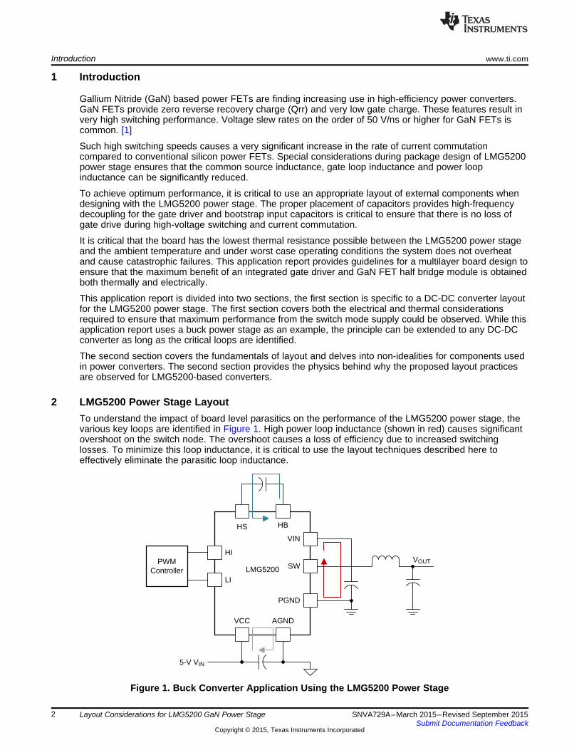
2 LMG5200 Power Stage LayoutTo understand the impact of board level parasitics on the performance of the LMG5200 power stage, thevarious key loops are identified in Figure 1. High power loop inductance (shown in red) causes significantovershoot on the switch node. The overshoot causes a loss of efficiency due to increased switchinglosses. To minimize this loop inductance, it is critical to use the layout techniques described here toeffectively eliminate the parasitic loop inductance.
Figure 1. Buck Converter Application Using the LMG5200 Power Stage
2 Layout Considerations for LMG5200 GaN Power Stage SNVA729A–March 2015–Revised September 2015Submit Documentation Feedback
Copyright © 2015, Texas Instruments Incorporated
VIN
PGND
SW
VIN
PGND
SWVCC AGND
HI
LI
HS HB
PGND
VIN Capacitors
LMG5200
Metal underneath solder mask
Metal 1
Metal 2 (PGND)
Legend
Vias
www.ti.com LMG5200 Power Stage Layout
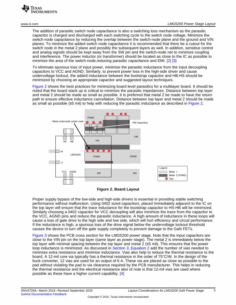
The addition of parasitic switch node capacitance is also a switching loss mechanism as the parasiticcapacitor is charged and discharged with each switching cycle to the switch node voltage. Minimize theswitch-node capacitance by reducing the overlap between the switch-node plane and the ground and VINplanes. To minimize the added switch node capacitance it is recommended that there be a cutout for theswitch node in the metal 2 plane and possibly the subsequent layers as well. In addition, sensitive controland analog signals should be kept away from the SW pin and the switch-node net to minimize couplingand interference. The power inductor (or transformer) should be located as close to the IC as possible tominimize the area of the switch-node,reducing parasitic capacitance and EMI. [2] [3]
To eliminate spurious loss of input power, minimize the parasitic inductance from the input decouplingcapacitors to VCC and AGND. Similarly, to prevent power loss in the high-side driver and causeundervoltage lockout, the added inductance between the bootstrap capacitor and HB-HS should beminimized by choosing an appropriate capacitor and suggested layout techniques.
Figure 2 shows the best practices for minimizing board level parasitics for a multilayer board. It should benoted that the board stack up is critical to minimize the parasitic impedances. Distance between top layerand metal 2 should be made as small as possible. It is preferred that metal 2 be made to have the returnpath to ensure effective inductance cancellation. Distance between top layer and metal 2 should be madeas small as possible (≤5 mil) to help with reducing the parasitic inductance as described in Figure 2.
Figure 2. Board Layout
Proper supply bypass of the low-side and high-side drivers is essential in providing stable switchingperformance without malfunction. Using 0402 sized capacitors, placed immediately adjacent to the IC onthe top layer will ensure that the trace inductance for the bootstrap capacitor to HS-HB will be minimized.Similarly choosing a 0402 capacitor for VCC decoupling will also minimize the trace from the capacitor tothe VCC, AGND pins and reduce the parasitic inductance. A high amount of inductance in these loops willcause a loss of gate drive to the high side and low side, which will hurt efficiency and circuit performance.If the inductance is high, a spurious loss of the drive signal below the undervoltage lockout thresholdcauses the device to turn off the gate supply completely to prevent damage to the GaN FETs.
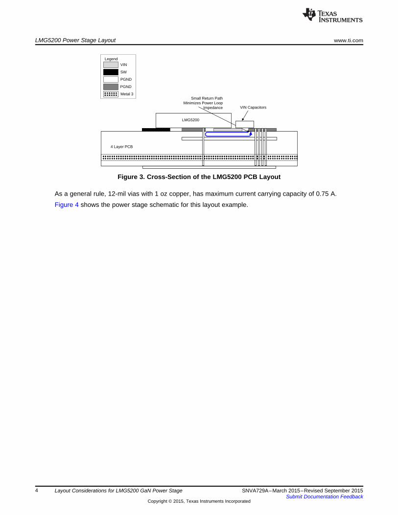
Figure 3 shows the PCB cross section for the LMG5200 power stage. Note that the input capacitors areclose to the VIN pin on the top layer (same layer as power stage). The metal 2 is immediately below thetop layer with minimal spacing between the top layer and metal 2 (≤5 mil). This ensures that the powerloop inductance is minimized. As discussed in Section 3, Equation 2 add the number of vias needed tominimize extra resistance and minimize inductance. Vias also help to reduce the thermal resistance to theboard. A 12-mil core via typically has a thermal resistance in the order of 75°C/W. In the design of thebuck converter, 12 vias are used for an output of 6 A. These via are placed as close as possible to thepad without violating the pad to via clearance required by the PCB manufacturer. This helps in reducingthe thermal resistance and the electrical resistance also of note is that 12-mil vias are used wherepossible as these have a higher current capability. [4]
3SNVA729A–March 2015–Revised September 2015 Layout Considerations for LMG5200 GaN Power StageSubmit Documentation Feedback
Copyright © 2015, Texas Instruments Incorporated
LMG5200
VIN Capacitors
4 Layer PCB
Small Return Path Minimizes Power Loop
Impedance
xxx
SW
VIN
PGND
Metal 3
PGND
Legend
LMG5200 Power Stage Layout www.ti.com
Figure 3. Cross-Section of the LMG5200 PCB Layout
As a general rule, 12-mil vias with 1 oz copper, has maximum current carrying capacity of 0.75 A.
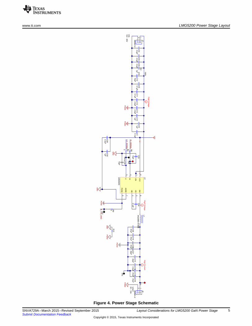
Figure 4 shows the power stage schematic for this layout example.
4 Layout Considerations for LMG5200 GaN Power Stage SNVA729A–March 2015–Revised September 2015Submit Documentation Feedback
Copyright © 2015, Texas Instruments Incorporated
22µ
FC
21
22µ
FC
15
2.2
µF
C16
1µ
FC
30
PG
ND
PG
ND
PG
ND
VO
UT
5V
- 10A
0.1
µF
C24
L1
XA
L8080-4
72M
E
TP
2
TP
3
VIN
10V
- 60V
K_V
IN_G
ND
TP
7
GN
D
47µ
FC
20
i
Hig
hV
olta
ge
i
Hig
hC
urre
nt
1µ
FC
9
PG
ND
0 R9
GN
DP
GN
D
0 R10
2.2
µF
C29
47µ
FC
19
47µ
FC
17
10pF
C23
GN
D
0 R6
0 R7
LO
_S
IGN
AL
VIN
1
HB
2
HS
3
HI
4
LI
5
VC
C6
AG
ND
7
SW
8
PG
ND
9
U1
LM
G5200
10pF
C25
HI_
SIG
NA
L
47µ
FC
18
10µ
F
100V
X7S
C10
2.2
µF
C12
2.2
µF
C13
1µ
FC
14
PG
ND
i
Hig
hV
olta
ge
0.1
µF
C11
0.1
µF
C8
TP
9
TP
10
47µ
FC
36
12
J1
282841-2
12
J2
282841-2
1µ
F
C2
2.2
µF
C6
2.2
µF
C5
2.2
µF
C4
0.1
µF
C1
VC
C
www.ti.com LMG5200 Power Stage Layout
Figure 4. Power Stage Schematic
5SNVA729A–March 2015–Revised September 2015 Layout Considerations for LMG5200 GaN Power StageSubmit Documentation Feedback
Copyright © 2015, Texas Instruments Incorporated
LMG5200 Power Stage Layout www.ti.com
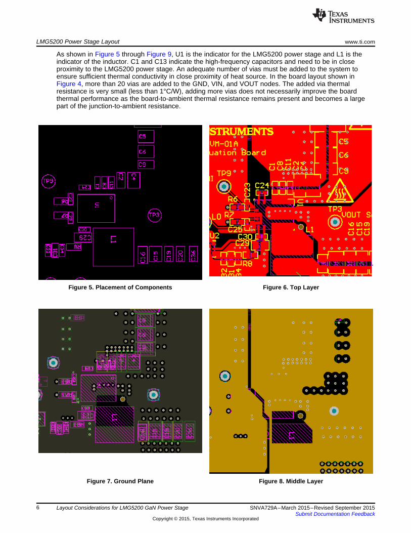
As shown in Figure 5 through Figure 9, U1 is the indicator for the LMG5200 power stage and L1 is theindicator of the inductor. C1 and C13 indicate the high-frequency capacitors and need to be in closeproximity to the LMG5200 power stage. An adequate number of vias must be added to the system toensure sufficient thermal conductivity in close proximity of heat source. In the board layout shown inFigure 4, more than 20 vias are added to the GND, VIN, and VOUT nodes. The added via thermalresistance is very small (less than 1°C/W), adding more vias does not necessarily improve the boardthermal performance as the board-to-ambient thermal resistance remains present and becomes a largepart of the junction-to-ambient resistance.
Figure 5. Placement of Components Figure 6. Top Layer
Figure 7. Ground Plane Figure 8. Middle Layer
6 Layout Considerations for LMG5200 GaN Power Stage SNVA729A–March 2015–Revised September 2015Submit Documentation Feedback
Copyright © 2015, Texas Instruments Incorporated
www.ti.com LMG5200 Power Stage Layout
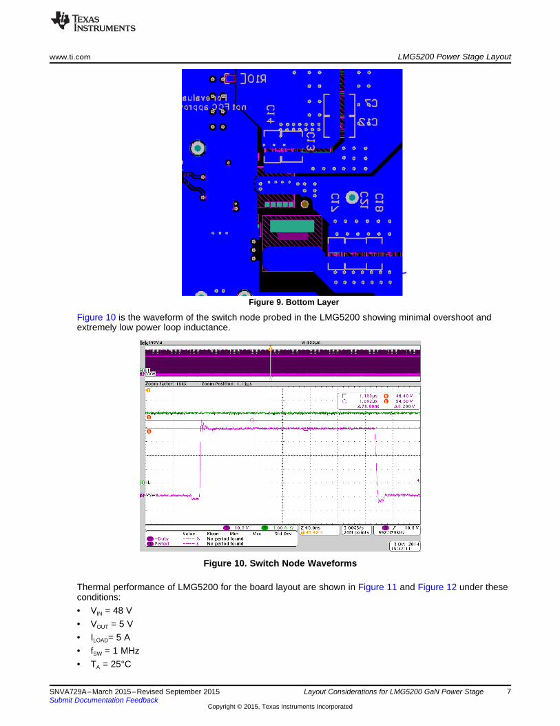
Figure 9. Bottom Layer
Figure 10 is the waveform of the switch node probed in the LMG5200 showing minimal overshoot andextremely low power loop inductance.
Figure 10. Switch Node Waveforms
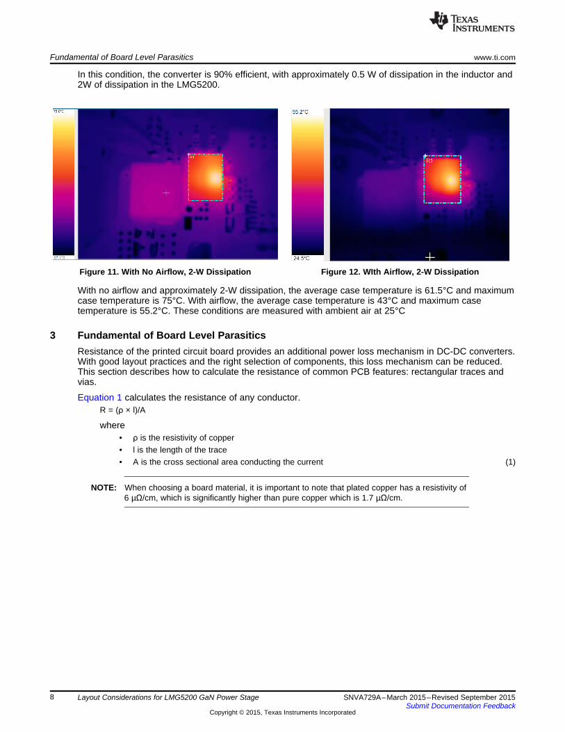
Thermal performance of LMG5200 for the board layout are shown in Figure 11 and Figure 12 under theseconditions:• VIN = 48 V• VOUT = 5 V• ILOAD= 5 A• fSW = 1 MHz• TA = 25°C
7SNVA729A–March 2015–Revised September 2015 Layout Considerations for LMG5200 GaN Power StageSubmit Documentation Feedback
Copyright © 2015, Texas Instruments Incorporated
Fundamental of Board Level Parasitics www.ti.com
In this condition, the converter is 90% efficient, with approximately 0.5 W of dissipation in the inductor and2W of dissipation in the LMG5200.
Figure 11. With No Airflow, 2-W Dissipation Figure 12. WIth Airflow, 2-W Dissipation
With no airflow and approximately 2-W dissipation, the average case temperature is 61.5°C and maximumcase temperature is 75°C. With airflow, the average case temperature is 43°C and maximum casetemperature is 55.2°C. These conditions are measured with ambient air at 25°C
3 Fundamental of Board Level ParasiticsResistance of the printed circuit board provides an additional power loss mechanism in DC-DC converters.With good layout practices and the right selection of components, this loss mechanism can be reduced.This section describes how to calculate the resistance of common PCB features: rectangular traces andvias.
Equation 1 calculates the resistance of any conductor.R = (ρ × l)/A
where• ρ is the resistivity of copper• l is the length of the trace• A is the cross sectional area conducting the current (1)
NOTE: When choosing a board material, it is important to note that plated copper has a resistivity of6 µΩ/cm, which is significantly higher than pure copper which is 1.7 µΩ/cm.
8 Layout Considerations for LMG5200 GaN Power Stage SNVA729A–March 2015–Revised September 2015Submit Documentation Feedback
Copyright © 2015, Texas Instruments Incorporated
´ ´ ´
=
2 H v lL
W
æ öæ ö= ´ ´ +ç ÷ç ÷+è øè ø
1 1L 2 l ln
T W 2
R =Ol
N × (r02F r1
2)
www.ti.com Fundamental of Board Level Parasitics
Vias on PCBs use plated copper where the resistance is significantly higher, so an adequate number ofvias should be considered when designing boards for high current. In some PCBs, plating is also appliedto the surface (top and bottom layers) to increase the copper thickness. If the board is designed to be aone-plate-one board, this implies that the addition of the extra plated copper only provides about 25%reduction for in the resistance for a 2 oz. board compared to a 1 oz. board with no plated copper.
NOTE: Copper resistance varies linearly with temperature and doubles from 25°C to 280°C.
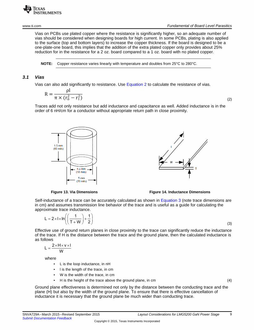
3.1 ViasVias can also add significantly to resistance. Use Equation 2 to calculate the resistance of vias.
(2)
Traces add not only resistance but add inductance and capacitance as well. Added inductance is in theorder of 6 nH/cm for a conductor without appropriate return path in close proximity.
Figure 13. Via Dimensions Figure 14. Inductance Dimensions
Self-inductance of a trace can be accurately calculated as shown in Equation 3 (note trace dimensions arein cm) and assumes transmission line behavior of the trace and is useful as a guide for calculating theapproximate trace inductance.
(3)
Effective use of ground return planes in close proximity to the trace can significantly reduce the inductanceof the trace. If H is the distance between the trace and the ground plane, then the calculated inductance isas follows
where• L is the loop inductance, in nH• l is the length of the trace, in cm• W is the width of the trace, in cm• H is the height of the trace above the ground plane, in cm (4)
Ground plane effectiveness is determined not only by the distance between the conducting trace and theplane (H) but also by the width of the ground plane. To ensure that there is effective cancellation ofinductance it is necessary that the ground plane be much wider than conducting trace.
9SNVA729A–March 2015–Revised September 2015 Layout Considerations for LMG5200 GaN Power StageSubmit Documentation Feedback
Copyright © 2015, Texas Instruments Incorporated

C =B0 × Br × A
t
Conclusion www.ti.com
Knowing the impact of ground planes on effective cancellation of inductance, this technique can be usedto significantly reduce the power loop inductance and gate loop inductance. Because these loops carrysignificant .
Capacitive coupling between PCB layers can yield advantages and disadvantages in power PCB design.The capacitance between traces can be identified as described in Equation 5.
where• A is the area of the copper planes• εr is the relative permittivity of the PCB dielectric• ε0 is the permittivity of air• t is the distance between the conductors (in meters) (5)
Capacitive coupling can be used to advantage for creating coupling between the input and ground planeswhich can be used for high frequency decoupling in addition to the decoupling capacitors added to thesystem. Also it is important to note that to minimize the switching node capacitance a cutout directlyunderneath the inductor and the associated traces in the PGND plane and the subsequent planes helpsminimize the added parasitic capacitance on the switch node.
4 ConclusionGaN FETS are finding use in high frequency DC-DC converters. Special layout techniques are required toensure that maximum performance of the DC-DC converter is obtained. Advantages and disadvantages ofsome commonly used techniques to design for the LMG5200 power stage have also been discussed. Afundamental overview on board level parasitics has been provided as a background for some of the layoutchoices that are made which should provide the designer with best practices for high frequency DC-DCconverters board design.
5 References
1. White Paper: Advancing Power Supply Solutions Through the Promise of GaN (SSZY017)2. Application Report: Layout Tips for EMI Reduction in DC / DC Converters (SNVA638)3. Henry Ott, Noise Reduction Techniques in Electronic Systems (John Wiley and Sons, 1988)4. Application Report: Semiconductor and IC Package Thermal Metrics (SPRA953)
10 Layout Considerations for LMG5200 GaN Power Stage SNVA729A–March 2015–Revised September 2015Submit Documentation Feedback
Copyright © 2015, Texas Instruments Incorporated

www.ti.com Revision History
Revision History
Changes from Original (March 2015) to A Revision ....................................................................................................... Page
• Changed typo in part number in graphic ............................................................................................... 3
NOTE: Page numbers for previous revisions may differ from page numbers in the current version.
11SNVA729A–March 2015–Revised September 2015 Revision HistorySubmit Documentation Feedback
Copyright © 2015, Texas Instruments Incorporated

IMPORTANT NOTICE
Texas Instruments Incorporated and its subsidiaries (TI) reserve the right to make corrections, enhancements, improvements and otherchanges to its semiconductor products and services per JESD46, latest issue, and to discontinue any product or service per JESD48, latestissue. Buyers should obtain the latest relevant information before placing orders and should verify that such information is current andcomplete. All semiconductor products (also referred to herein as “components”) are sold subject to TI’s terms and conditions of salesupplied at the time of order acknowledgment.TI warrants performance of its components to the specifications applicable at the time of sale, in accordance with the warranty in TI’s termsand conditions of sale of semiconductor products. Testing and other quality control techniques are used to the extent TI deems necessaryto support this warranty. Except where mandated by applicable law, testing of all parameters of each component is not necessarilyperformed.TI assumes no liability for applications assistance or the design of Buyers’ products. Buyers are responsible for their products andapplications using TI components. To minimize the risks associated with Buyers’ products and applications, Buyers should provideadequate design and operating safeguards.TI does not warrant or represent that any license, either express or implied, is granted under any patent right, copyright, mask work right, orother intellectual property right relating to any combination, machine, or process in which TI components or services are used. Informationpublished by TI regarding third-party products or services does not constitute a license to use such products or services or a warranty orendorsement thereof. Use of such information may require a license from a third party under the patents or other intellectual property of thethird party, or a license from TI under the patents or other intellectual property of TI.Reproduction of significant portions of TI information in TI data books or data sheets is permissible only if reproduction is without alterationand is accompanied by all associated warranties, conditions, limitations, and notices. TI is not responsible or liable for such altereddocumentation. Information of third parties may be subject to additional restrictions.Resale of TI components or services with statements different from or beyond the parameters stated by TI for that component or servicevoids all express and any implied warranties for the associated TI component or service and is an unfair and deceptive business practice.TI is not responsible or liable for any such statements.Buyer acknowledges and agrees that it is solely responsible for compliance with all legal, regulatory and safety-related requirementsconcerning its products, and any use of TI components in its applications, notwithstanding any applications-related information or supportthat may be provided by TI. Buyer represents and agrees that it has all the necessary expertise to create and implement safeguards whichanticipate dangerous consequences of failures, monitor failures and their consequences, lessen the likelihood of failures that might causeharm and take appropriate remedial actions. Buyer will fully indemnify TI and its representatives against any damages arising out of the useof any TI components in safety-critical applications.In some cases, TI components may be promoted specifically to facilitate safety-related applications. With such components, TI’s goal is tohelp enable customers to design and create their own end-product solutions that meet applicable functional safety standards andrequirements. Nonetheless, such components are subject to these terms.No TI components are authorized for use in FDA Class III (or similar life-critical medical equipment) unless authorized officers of the partieshave executed a special agreement specifically governing such use.Only those TI components which TI has specifically designated as military grade or “enhanced plastic” are designed and intended for use inmilitary/aerospace applications or environments. Buyer acknowledges and agrees that any military or aerospace use of TI componentswhich have not been so designated is solely at the Buyer's risk, and that Buyer is solely responsible for compliance with all legal andregulatory requirements in connection with such use.TI has specifically designated certain components as meeting ISO/TS16949 requirements, mainly for automotive use. In any case of use ofnon-designated products, TI will not be responsible for any failure to meet ISO/TS16949.
Products ApplicationsAudio www.ti.com/audio Automotive and Transportation www.ti.com/automotiveAmplifiers amplifier.ti.com Communications and Telecom www.ti.com/communicationsData Converters dataconverter.ti.com Computers and Peripherals www.ti.com/computersDLP® Products www.dlp.com Consumer Electronics www.ti.com/consumer-appsDSP dsp.ti.com Energy and Lighting www.ti.com/energyClocks and Timers www.ti.com/clocks Industrial www.ti.com/industrialInterface interface.ti.com Medical www.ti.com/medicalLogic logic.ti.com Security www.ti.com/securityPower Mgmt power.ti.com Space, Avionics and Defense www.ti.com/space-avionics-defenseMicrocontrollers microcontroller.ti.com Video and Imaging www.ti.com/videoRFID www.ti-rfid.comOMAP Applications Processors www.ti.com/omap TI E2E Community e2e.ti.comWireless Connectivity www.ti.com/wirelessconnectivity
Mailing Address: Texas Instruments, Post Office Box 655303, Dallas, Texas 75265Copyright © 2015, Texas Instruments Incorporated