50A Digital DC/DC PMBus Power Module - Anglia · PDF file50A Digital DC/DC PMBus Power Module...
54
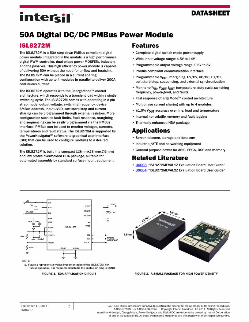
1 DATASHEET 50A Digital DC/DC PMBus Power Module ISL8272M The ISL8272M is a 50A step-down PMBus compliant digital power module. Integrated in the module is a high performance digital PWM controller, dual-phase power MOSFETs, inductors and the passives. This high efficiency power module is capable of delivering 50A without the need for airflow and heatsink. The ISL8272M can be placed in a current sharing configuration with up to 4 modules in parallel to deliver 200A continuous current. The ISL8272M operates with the ChargeMode™ control architecture, which responds to a transient load within a single switching cycle. The ISL8272M comes with operating in a pin strap mode; output voltage, switching frequency, device SMBus address, input UVLO, soft-start/stop and current sharing can be programmed through external resistors. More configuration such as fault limits, fault response, margining and sequencing can be easily programmed via the PMBus interface. PMBus can be used to monitor voltages, currents, temperatures and fault status. The ISL8272M is supported by the PowerNavigator™ software, a graphical user interface (GUI) that can be used to configure modules to a desired solution. The ISL8272M is built in a compact (18mmx23mmx7.5mm) and low profile overmolded HDA package, suitable for automated assembly by standard surface mount equipment. Features • Complete digital switch mode power supply • Wide input voltage range: 4.5V to 14V • Programmable output voltage range: 0.6V to 5V • PMBus compliant communication interface • Programmable V OUT , margining, UV/OV, UC/OC, UT/OT, soft-start/stop, sequencing, and external synchronization • Monitor of V IN , V OUT , I OUT , temperature, duty cycle, switching frequency, power-good, and faults • Fast response ChargeMode TM control architecture • Multiphase current sharing with up to 4 modules • ±1.0% V OUT accuracy over line, load and temperature • Internal nonvolatile memory and fault logging • Thermally enhanced HDA package Applications • Server, telecom, storage and datacom • Industrial/ATE and networking equipment • General purpose power for ASIC, FPGA, DSP and memory Related Literature • UG003 , “ISL8272MEVAL1Z Evaluation Board User Guide” • UG004 , “ISL8272MEVAL2Z Evaluation Board User Guide” FIGURE 1. 50A APPLICATION CIRCUIT FIGURE 2. A SMALL PACKAGE FOR HIGH POWER DENSITY VIN VDD VR55 VR5 VR VOUT SGND PGND VR6 VDRV SCL SDA SALRT VMON VCC VDRV1 VSENP VSENN VIN CIN ISL8272M VOUT PMBUS INTERFACE COUT 100k 2x10μF 10μF 10μF EN ENABLE 6.65k NOTE: 1. Figure 1 represents a typical implementation of the ISL8272M. For PMBus operation, it is recommended to tie the enable pin (EN) to SGND. 23mm 18mm 7.5mm September 17, 2014 FN8670.1 CAUTION: These devices are sensitive to electrostatic discharge; follow proper IC Handling Procedures. 1-888-INTERSIL or 1-888-468-3774 | Copyright Intersil Americas LLC 2014. All Rights Reserved Intersil (and design), ChargeMode, PowerNavigator and Digital-DC are trademarks owned by Intersil Corporation or one of its subsidiaries. All other trademarks mentioned are the property of their respective owners.
Transcript of 50A Digital DC/DC PMBus Power Module - Anglia · PDF file50A Digital DC/DC PMBus Power Module...
DATASHEET
50A Digital DC/DC PMBus Power ModuleISL8272MThe ISL8272M is a 50A step-down PMBus compliant digital power module. Integrated in the module is a high performance digital PWM controller, dual-phase power MOSFETs, inductors and the passives. This high efficiency power module is capable of delivering 50A without the need for airflow and heatsink. The ISL8272M can be placed in a current sharing configuration with up to 4 modules in parallel to deliver 200A continuous current.
The ISL8272M operates with the ChargeMode™ control architecture, which responds to a transient load within a single switching cycle. The ISL8272M comes with operating in a pin strap mode; output voltage, switching frequency, device SMBus address, input UVLO, soft-start/stop and current sharing can be programmed through external resistors. More configuration such as fault limits, fault response, margining and sequencing can be easily programmed via the PMBus interface. PMBus can be used to monitor voltages, currents, temperatures and fault status. The ISL8272M is supported by the PowerNavigator™ software, a graphical user interface (GUI) that can be used to configure modules to a desired solution.
The ISL8272M is built in a compact (18mmx23mmx7.5mm) and low profile overmolded HDA package, suitable for automated assembly by standard surface mount equipment.
Features• Complete digital switch mode power supply
• Wide input voltage range: 4.5V to 14V
• Programmable output voltage range: 0.6V to 5V
• PMBus compliant communication interface
• Programmable VOUT, margining, UV/OV, UC/OC, UT/OT, soft-start/stop, sequencing, and external synchronization
• Monitor of VIN, VOUT, IOUT, temperature, duty cycle, switching frequency, power-good, and faults
• Fast response ChargeModeTM control architecture
• Multiphase current sharing with up to 4 modules
• ±1.0% VOUT accuracy over line, load and temperature
• Internal nonvolatile memory and fault logging
• Thermally enhanced HDA package
Applications• Server, telecom, storage and datacom
• Industrial/ATE and networking equipment
• General purpose power for ASIC, FPGA, DSP and memory
Related Literature• UG003, “ISL8272MEVAL1Z Evaluation Board User Guide”
• UG004, “ISL8272MEVAL2Z Evaluation Board User Guide”
FIGURE 1. 50A APPLICATION CIRCUIT FIGURE 2. A SMALL PACKAGE FOR HIGH POWER DENSITY
VIN
VDD
VR55
VR5
VR
VOUT
SGND PGND
VR6
VDRV
SCL
SDA
SALRTVMON
VCC
VDRV1
VSENP
VSENN
VIN
CIN
ISL8272M
VOUT
PMBUS INTERFACE
COUT
100k 2x10µF
10µF 10µF
ENENABLE
6.65k
NOTE:1. Figure 1 represents a typical implementation of the ISL8272M. For
PMBus operation, it is recommended to tie the enable pin (EN) to SGND.
23mm
18mm
7.5mm
1September 17, 2014FN8670.1
CAUTION: These devices are sensitive to electrostatic discharge; follow proper IC Handling Procedures.1-888-INTERSIL or 1-888-468-3774 | Copyright Intersil Americas LLC 2014. All Rights Reserved
Intersil (and design), ChargeMode, PowerNavigator and Digital-DC are trademarks owned by Intersil Corporationor one of its subsidiaries. All other trademarks mentioned are the property of their respective owners.
ISL8272M
Table of ContentsOrdering Information . . . . . . . . . . . . . . . . . . . . . . . . . . . . . . . . . . . . . . . . . . . . . . . . . . . . . . . . . . . . . . . . . . . . . . . . . . . . . . . . . . . . . . . . 3
Pin Configuration. . . . . . . . . . . . . . . . . . . . . . . . . . . . . . . . . . . . . . . . . . . . . . . . . . . . . . . . . . . . . . . . . . . . . . . . . . . . . . . . . . . . . . . . . . . . 4
Pin Descriptions. . . . . . . . . . . . . . . . . . . . . . . . . . . . . . . . . . . . . . . . . . . . . . . . . . . . . . . . . . . . . . . . . . . . . . . . . . . . . . . . . . . . . . . . . . . . . 4
ISL8272M Internal Block Diagram . . . . . . . . . . . . . . . . . . . . . . . . . . . . . . . . . . . . . . . . . . . . . . . . . . . . . . . . . . . . . . . . . . . . . . . . . . . . . 6
Typical Application Circuit - Single Module . . . . . . . . . . . . . . . . . . . . . . . . . . . . . . . . . . . . . . . . . . . . . . . . . . . . . . . . . . . . . . . . . . . . . . 7
Typical Application Circuit - Three Module Current Sharing . . . . . . . . . . . . . . . . . . . . . . . . . . . . . . . . . . . . . . . . . . . . . . . . . . . . . . . . 8
Absolute Maximum Ratings . . . . . . . . . . . . . . . . . . . . . . . . . . . . . . . . . . . . . . . . . . . . . . . . . . . . . . . . . . . . . . . . . . . . . . . . . . . . . . . . . . 10
Thermal Information . . . . . . . . . . . . . . . . . . . . . . . . . . . . . . . . . . . . . . . . . . . . . . . . . . . . . . . . . . . . . . . . . . . . . . . . . . . . . . . . . . . . . . . . 10
Recommended Operating Conditions . . . . . . . . . . . . . . . . . . . . . . . . . . . . . . . . . . . . . . . . . . . . . . . . . . . . . . . . . . . . . . . . . . . . . . . . . 10
Electrical Specifications . . . . . . . . . . . . . . . . . . . . . . . . . . . . . . . . . . . . . . . . . . . . . . . . . . . . . . . . . . . . . . . . . . . . . . . . . . . . . . . . . . . . 10
Typical Performance Curves . . . . . . . . . . . . . . . . . . . . . . . . . . . . . . . . . . . . . . . . . . . . . . . . . . . . . . . . . . . . . . . . . . . . . . . . . . . . . . . . . 13
Efficiency Performance . . . . . . . . . . . . . . . . . . . . . . . . . . . . . . . . . . . . . . . . . . . . . . . . . . . . . . . . . . . . . . . . . . . . . . . . . . . . . . . . . . . . . 13
Transient Response Performance . . . . . . . . . . . . . . . . . . . . . . . . . . . . . . . . . . . . . . . . . . . . . . . . . . . . . . . . . . . . . . . . . . . . . . . . . . . . 14
Derating Curves . . . . . . . . . . . . . . . . . . . . . . . . . . . . . . . . . . . . . . . . . . . . . . . . . . . . . . . . . . . . . . . . . . . . . . . . . . . . . . . . . . . . . . . . . . . . 15
Functional Description . . . . . . . . . . . . . . . . . . . . . . . . . . . . . . . . . . . . . . . . . . . . . . . . . . . . . . . . . . . . . . . . . . . . . . . . . . . . . . . . . . . . . . 17SMBus Communications. . . . . . . . . . . . . . . . . . . . . . . . . . . . . . . . . . . . . . . . . . . . . . . . . . . . . . . . . . . . . . . . . . . . . . . . . . . . . . . . . . . . . . . . . . 17Output Voltage Selection . . . . . . . . . . . . . . . . . . . . . . . . . . . . . . . . . . . . . . . . . . . . . . . . . . . . . . . . . . . . . . . . . . . . . . . . . . . . . . . . . . . . . . . . . 17Soft-Start/Stop Delay and Ramp Times . . . . . . . . . . . . . . . . . . . . . . . . . . . . . . . . . . . . . . . . . . . . . . . . . . . . . . . . . . . . . . . . . . . . . . . . . . . . . 17Power-Good . . . . . . . . . . . . . . . . . . . . . . . . . . . . . . . . . . . . . . . . . . . . . . . . . . . . . . . . . . . . . . . . . . . . . . . . . . . . . . . . . . . . . . . . . . . . . . . . . . . . 18Switching Frequency and PLL . . . . . . . . . . . . . . . . . . . . . . . . . . . . . . . . . . . . . . . . . . . . . . . . . . . . . . . . . . . . . . . . . . . . . . . . . . . . . . . . . . . . . 18Loop Compensation . . . . . . . . . . . . . . . . . . . . . . . . . . . . . . . . . . . . . . . . . . . . . . . . . . . . . . . . . . . . . . . . . . . . . . . . . . . . . . . . . . . . . . . . . . . . . 18Input Undervoltage Lockout (UVLO). . . . . . . . . . . . . . . . . . . . . . . . . . . . . . . . . . . . . . . . . . . . . . . . . . . . . . . . . . . . . . . . . . . . . . . . . . . . . . . . . 19SMBus Module Address Selection . . . . . . . . . . . . . . . . . . . . . . . . . . . . . . . . . . . . . . . . . . . . . . . . . . . . . . . . . . . . . . . . . . . . . . . . . . . . . . . . . . 19Output Overvoltage Protection. . . . . . . . . . . . . . . . . . . . . . . . . . . . . . . . . . . . . . . . . . . . . . . . . . . . . . . . . . . . . . . . . . . . . . . . . . . . . . . . . . . . . 19Output Prebias Protection . . . . . . . . . . . . . . . . . . . . . . . . . . . . . . . . . . . . . . . . . . . . . . . . . . . . . . . . . . . . . . . . . . . . . . . . . . . . . . . . . . . . . . . . 20Output Overcurrent Protection . . . . . . . . . . . . . . . . . . . . . . . . . . . . . . . . . . . . . . . . . . . . . . . . . . . . . . . . . . . . . . . . . . . . . . . . . . . . . . . . . . . . . 20Thermal Overload Protection . . . . . . . . . . . . . . . . . . . . . . . . . . . . . . . . . . . . . . . . . . . . . . . . . . . . . . . . . . . . . . . . . . . . . . . . . . . . . . . . . . . . . . 20Digital-DC™ Bus . . . . . . . . . . . . . . . . . . . . . . . . . . . . . . . . . . . . . . . . . . . . . . . . . . . . . . . . . . . . . . . . . . . . . . . . . . . . . . . . . . . . . . . . . . . . . . . . . 20Active Current Sharing . . . . . . . . . . . . . . . . . . . . . . . . . . . . . . . . . . . . . . . . . . . . . . . . . . . . . . . . . . . . . . . . . . . . . . . . . . . . . . . . . . . . . . . . . . . 21Phase Spreading . . . . . . . . . . . . . . . . . . . . . . . . . . . . . . . . . . . . . . . . . . . . . . . . . . . . . . . . . . . . . . . . . . . . . . . . . . . . . . . . . . . . . . . . . . . . . . . . 22Fault Spreading . . . . . . . . . . . . . . . . . . . . . . . . . . . . . . . . . . . . . . . . . . . . . . . . . . . . . . . . . . . . . . . . . . . . . . . . . . . . . . . . . . . . . . . . . . . . . . . . . 22Output Sequencing . . . . . . . . . . . . . . . . . . . . . . . . . . . . . . . . . . . . . . . . . . . . . . . . . . . . . . . . . . . . . . . . . . . . . . . . . . . . . . . . . . . . . . . . . . . . . . 22Monitoring Via SMBus . . . . . . . . . . . . . . . . . . . . . . . . . . . . . . . . . . . . . . . . . . . . . . . . . . . . . . . . . . . . . . . . . . . . . . . . . . . . . . . . . . . . . . . . . . . . 22Snapshot Parameter Capture . . . . . . . . . . . . . . . . . . . . . . . . . . . . . . . . . . . . . . . . . . . . . . . . . . . . . . . . . . . . . . . . . . . . . . . . . . . . . . . . . . . . . 22Nonvolatile Memory . . . . . . . . . . . . . . . . . . . . . . . . . . . . . . . . . . . . . . . . . . . . . . . . . . . . . . . . . . . . . . . . . . . . . . . . . . . . . . . . . . . . . . . . . . . . . 22
Layout Guide. . . . . . . . . . . . . . . . . . . . . . . . . . . . . . . . . . . . . . . . . . . . . . . . . . . . . . . . . . . . . . . . . . . . . . . . . . . . . . . . . . . . . . . . . . . . . . . 23
Thermal Considerations . . . . . . . . . . . . . . . . . . . . . . . . . . . . . . . . . . . . . . . . . . . . . . . . . . . . . . . . . . . . . . . . . . . . . . . . . . . . . . . . . . . . . 23Package Description . . . . . . . . . . . . . . . . . . . . . . . . . . . . . . . . . . . . . . . . . . . . . . . . . . . . . . . . . . . . . . . . . . . . . . . . . . . . . . . . . . . . . . . . . . . . . 23PCB Layout Pattern Design . . . . . . . . . . . . . . . . . . . . . . . . . . . . . . . . . . . . . . . . . . . . . . . . . . . . . . . . . . . . . . . . . . . . . . . . . . . . . . . . . . . . . . . 24Thermal Vias. . . . . . . . . . . . . . . . . . . . . . . . . . . . . . . . . . . . . . . . . . . . . . . . . . . . . . . . . . . . . . . . . . . . . . . . . . . . . . . . . . . . . . . . . . . . . . . . . . . . 24Stencil Pattern Design . . . . . . . . . . . . . . . . . . . . . . . . . . . . . . . . . . . . . . . . . . . . . . . . . . . . . . . . . . . . . . . . . . . . . . . . . . . . . . . . . . . . . . . . . . . 24Reflow Parameters . . . . . . . . . . . . . . . . . . . . . . . . . . . . . . . . . . . . . . . . . . . . . . . . . . . . . . . . . . . . . . . . . . . . . . . . . . . . . . . . . . . . . . . . . . . . . . 24
PMBus Command Summary . . . . . . . . . . . . . . . . . . . . . . . . . . . . . . . . . . . . . . . . . . . . . . . . . . . . . . . . . . . . . . . . . . . . . . . . . . . . . . . . . . 25
PMBus™ Data Formats . . . . . . . . . . . . . . . . . . . . . . . . . . . . . . . . . . . . . . . . . . . . . . . . . . . . . . . . . . . . . . . . . . . . . . . . . . . . . . . . . . . . . . 28
PMBus Commands Description . . . . . . . . . . . . . . . . . . . . . . . . . . . . . . . . . . . . . . . . . . . . . . . . . . . . . . . . . . . . . . . . . . . . . . . . . . . . . . . 29
Datasheet Revision History . . . . . . . . . . . . . . . . . . . . . . . . . . . . . . . . . . . . . . . . . . . . . . . . . . . . . . . . . . . . . . . . . . . . . . . . . . . . . . . . . . 49
Firmware Revision History . . . . . . . . . . . . . . . . . . . . . . . . . . . . . . . . . . . . . . . . . . . . . . . . . . . . . . . . . . . . . . . . . . . . . . . . . . . . . . . . . . . 49
About Intersil . . . . . . . . . . . . . . . . . . . . . . . . . . . . . . . . . . . . . . . . . . . . . . . . . . . . . . . . . . . . . . . . . . . . . . . . . . . . . . . . . . . . . . . . . . . . . . 49
Package Outline Drawing . . . . . . . . . . . . . . . . . . . . . . . . . . . . . . . . . . . . . . . . . . . . . . . . . . . . . . . . . . . . . . . . . . . . . . . . . . . . . . . . . . . . 50
2 FN8670.1September 17, 2014
Submit Document Feedback
ISL8272M
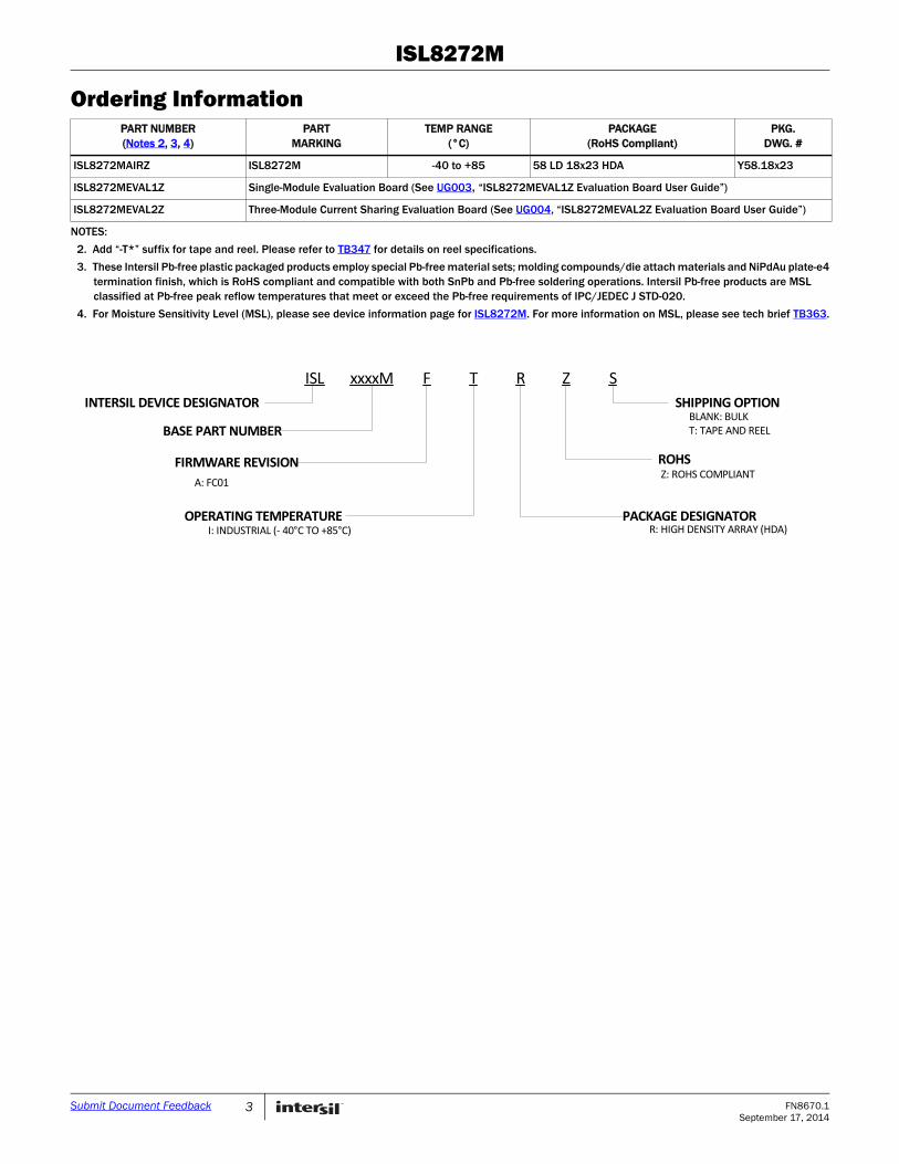
Ordering InformationPART NUMBER(Notes 2, 3, 4)
PART MARKING
TEMP RANGE(°C)
PACKAGE(RoHS Compliant)
PKG. DWG. #
ISL8272MAIRZ ISL8272M -40 to +85 58 LD 18x23 HDA Y58.18x23
ISL8272MEVAL1Z Single-Module Evaluation Board (See UG003, “ISL8272MEVAL1Z Evaluation Board User Guide”)
ISL8272MEVAL2Z Three-Module Current Sharing Evaluation Board (See UG004, “ISL8272MEVAL2Z Evaluation Board User Guide”)
NOTES:
2. Add “-T*” suffix for tape and reel. Please refer to TB347 for details on reel specifications.
3. These Intersil Pb-free plastic packaged products employ special Pb-free material sets; molding compounds/die attach materials and NiPdAu plate-e4 termination finish, which is RoHS compliant and compatible with both SnPb and Pb-free soldering operations. Intersil Pb-free products are MSL classified at Pb-free peak reflow temperatures that meet or exceed the Pb-free requirements of IPC/JEDEC J STD-020.
4. For Moisture Sensitivity Level (MSL), please see device information page for ISL8272M. For more information on MSL, please see tech brief TB363.
ISL xxxxM F T R Z S
INTERSIL DEVICE DESIGNATOR
BASE PART NUMBER
FIRMWARE REVISION
A: FC01
OPERATING TEMPERATUREI: INDUSTRIAL (‐ 40°C TO +85°C)
SHIPPING OPTIONBLANK: BULKT: TAPE AND REEL
ROHSZ: ROHS COMPLIANT
PACKAGE DESIGNATORR: HIGH DENSITY ARRAY (HDA)
3 FN8670.1September 17, 2014
Submit Document Feedback
ISL8272M
Pin ConfigurationISL8272M
(58 LD HDA)TOP VIEW
A
B
C
D
E
F
G
H
J
K
L
M
N
P
R
T
U
V
W
Y
AA
AB
AC
1 2 3 4 5 6 7 8 9 10 11 12 13 14 15 16 17 18
PAD1 PAD2
PAD8
PAD9 PAD10 PAD11 PAD12
PAD6
PAD13
PAD14
PAD15
PAD16
PAD3
PAD4
PAD5
PAD7
VOUT VOUT
PGND PGND
PGNDPGND
PGND PGND
SGND
SGND SGND
SW1 SW2
VIN VIN
VIN DCMDCM
SWD2VDRVPGND
PGNDSWD1VR
VCC
VSENPVSENN
TEST
TEST
DDC
SS/UVLO
PG
VSETTEST
CS
MGN SA
SALRT SDA
SCL
VMON
SYNC
TEST
EN
TEST
TEST
V25ASCR
SGND
VDD
VR5
SGNDVR6
VDRV
PGND
VR55
PGND PGND
VDRV1 VDRV1
Pin Descriptions PIN LABEL TYPE DESCRIPTION
PAD1, 2 VOUT PWR Power supply output voltage. Output voltage from 0.6V to 5V. Tie these two pins together to achieve a single output. For higher output voltage, refer to the derating curves starting on page 15 to set the maximum output current from these pads.
PAD 3, 4, 5, 7, 10, 12, 13, 15
PGND PWR Power ground. Refer to the “Layout Guide” on page 23 for the PGND pad connections and I/O capacitor placement.
PAD 6 SGND PWR Signal ground. Refer to “Layout Guide” on page 23 for the SGND pad connections.
PAD 8, 9, 11 VIN PWR Input power supply voltage to power the module. Input voltage range from 4.5V to 14V.
PAD 14, 16 SW1, SW2
PWR Switching node pads. The SW pads are used to dissipate the heat and provide the good thermal performance. Refer to “Layout Guide” on page 23 for the SW pad connections.
C6 VSET I Output voltage selection pin. Used to set VOUT set point and VOUT max.
C7 CS I Current sharing configuration pin. Used to program current sharing configurations such as SYNC selection, phase spreading and VOUT droop.
C8 MGN I External VOUT margin control pin. Active high (>2V) sets VOUT margin high; active low (<0.8V) sets VOUT margin low; high impedance (floating) sets VOUT to normal voltage. Factory default range for margining is nominal VOUT ±5%. When using PMBus to control margin command, leave this pin as no connection.
C9 VMON I Driver voltage monitoring. Use this pin to monitor VDRV through an external 16:1 resistor divider.
C10 SA I Serial address selection pin. Used to assign unique address for each individual device or to enable certain management features.
C11 SALRT O Serial alert. Connect to external host if desired. SALRT is asserted low upon a warning or a fault event and deasserted when warning or fault is cleared. A pull-up resistor is required.
4 FN8670.1September 17, 2014
Submit Document Feedback
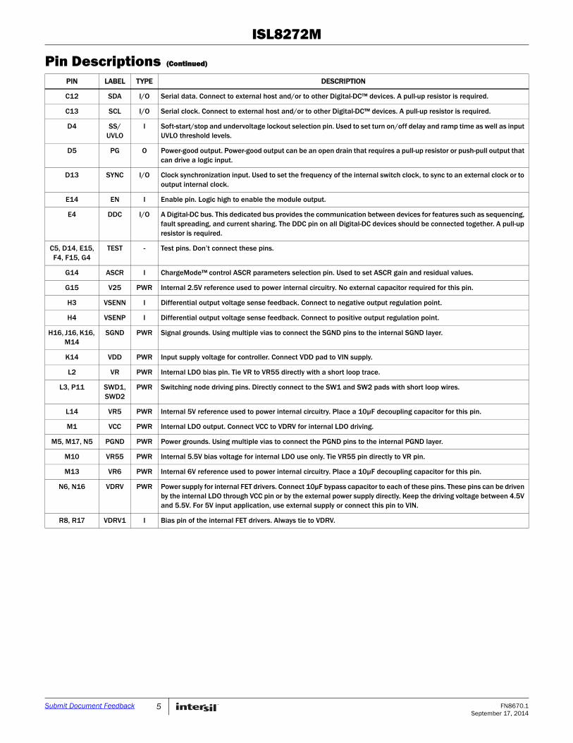
ISL8272M
C12 SDA I/O Serial data. Connect to external host and/or to other Digital-DC™ devices. A pull-up resistor is required.
C13 SCL I/O Serial clock. Connect to external host and/or to other Digital-DC™ devices. A pull-up resistor is required.
D4 SS/ UVLO
I Soft-start/stop and undervoltage lockout selection pin. Used to set turn on/off delay and ramp time as well as input UVLO threshold levels.
D5 PG O Power-good output. Power-good output can be an open drain that requires a pull-up resistor or push-pull output that can drive a logic input.
D13 SYNC I/O Clock synchronization input. Used to set the frequency of the internal switch clock, to sync to an external clock or to output internal clock.
E14 EN I Enable pin. Logic high to enable the module output.
E4 DDC I/O A Digital-DC bus. This dedicated bus provides the communication between devices for features such as sequencing, fault spreading, and current sharing. The DDC pin on all Digital-DC devices should be connected together. A pull-up resistor is required.
C5, D14, E15, F4, F15, G4
TEST - Test pins. Don’t connect these pins.
G14 ASCR I ChargeMode™ control ASCR parameters selection pin. Used to set ASCR gain and residual values.
G15 V25 PWR Internal 2.5V reference used to power internal circuitry. No external capacitor required for this pin.
H3 VSENN I Differential output voltage sense feedback. Connect to negative output regulation point.
H4 VSENP I Differential output voltage sense feedback. Connect to positive output regulation point.
H16, J16, K16, M14
SGND PWR Signal grounds. Using multiple vias to connect the SGND pins to the internal SGND layer.
K14 VDD PWR Input supply voltage for controller. Connect VDD pad to VIN supply.
L2 VR PWR Internal LDO bias pin. Tie VR to VR55 directly with a short loop trace.
L3, P11 SWD1,SWD2
PWR Switching node driving pins. Directly connect to the SW1 and SW2 pads with short loop wires.
L14 VR5 PWR Internal 5V reference used to power internal circuitry. Place a 10µF decoupling capacitor for this pin.
M1 VCC PWR Internal LDO output. Connect VCC to VDRV for internal LDO driving.
M5, M17, N5 PGND PWR Power grounds. Using multiple vias to connect the PGND pins to the internal PGND layer.
M10 VR55 PWR Internal 5.5V bias voltage for internal LDO use only. Tie VR55 pin directly to VR pin.
M13 VR6 PWR Internal 6V reference used to power internal circuitry. Place a 10µF decoupling capacitor for this pin.
N6, N16 VDRV PWR Power supply for internal FET drivers. Connect 10μF bypass capacitor to each of these pins. These pins can be driven by the internal LDO through VCC pin or by the external power supply directly. Keep the driving voltage between 4.5V and 5.5V. For 5V input application, use external supply or connect this pin to VIN.
R8, R17 VDRV1 I Bias pin of the internal FET drivers. Always tie to VDRV.
Pin Descriptions (Continued)
PIN LABEL TYPE DESCRIPTION
5 FN8670.1September 17, 2014
Submit Document Feedback
ISL8272M
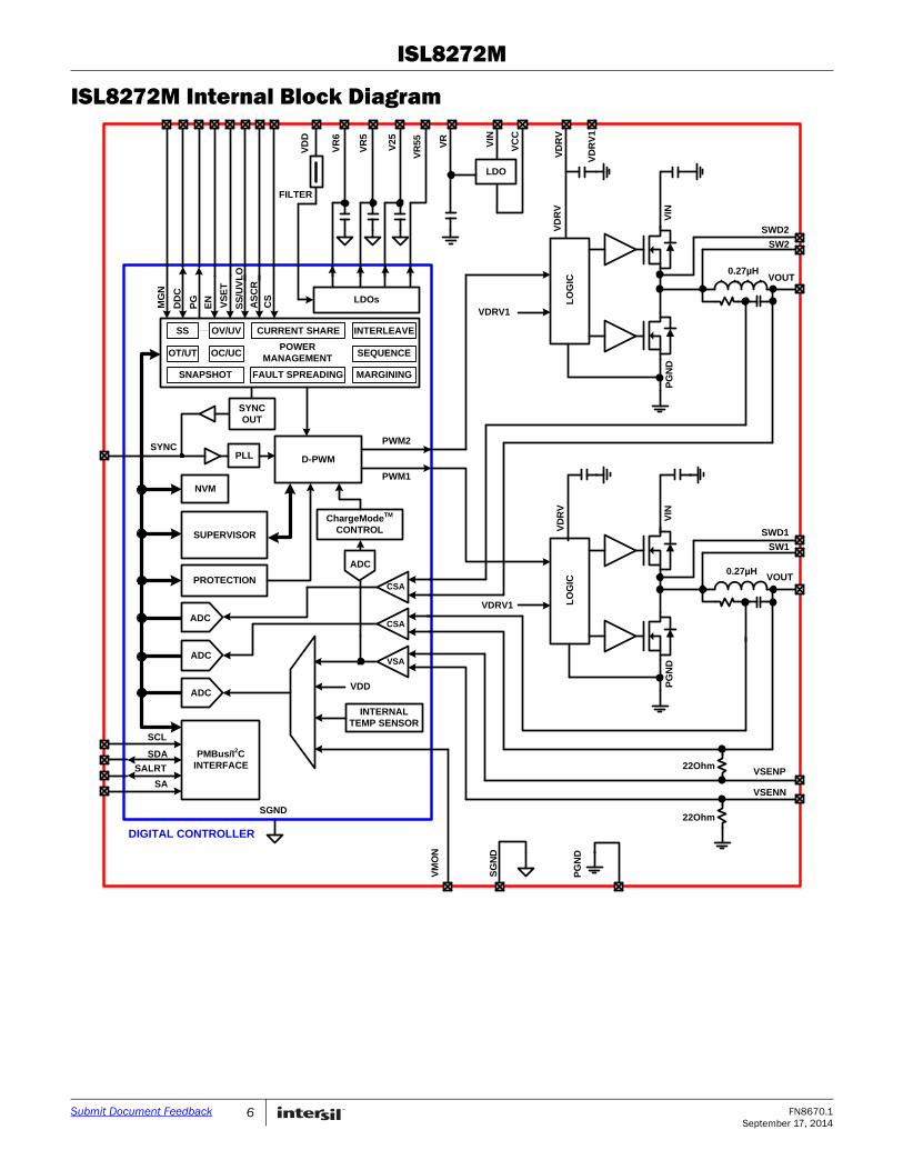
ISL8272M Internal Block Diagram
DIGITAL CONTROLLER
PG
ND
SG
ND
VS
ET
SCL
SALRT
SA
EN
PG
SYNC
SGND
PWM2
PMBus/I2CINTERFACE
SDA
ADC
CSA
VSA
SUPERVISOR
INTERNAL TEMP SENSOR
PROTECTION
OC/UC
D-PWMPLL
SYNC OUT
POWER MANAGEMENT
SS
MARGINING
OV/UV CURRENT SHARE INTERLEAVE
SEQUENCE
NVM
VDD
DD
C
SNAPSHOT FAULT SPREADING
OT/UT
VOUT0.27µH
LO
GIC
VIN
PG
ND
VIN
VD
RV
VR
6
VSENP
MG
N
VM
ON
ADC
VR
5
V25
LDOs
VR
55
VD
D
FILTER
VOUT0.27µH
LO
GIC
VIN
PG
ND
CSA
ChargeModeTM
CONTROL
ADC
PWM1
VR
VDRV1
VDRV1
VD
RV
VD
RV
VC
C
SS
/UV
LO
AS
CR
CS
VD
RV
1
SWD2
SW2
SWD1
SW1
VSENN
22Ohm
22Ohm
LDO
ADC
6 FN8670.1September 17, 2014
Submit Document Feedback
ISL8272M
7FN
86
70
.1Septem
ber 17, 2
014S
ubmit D
ocument Feedback
VOUT1.2V 50A
100µFRAMIC
4x470µF POSCAP
8 C9
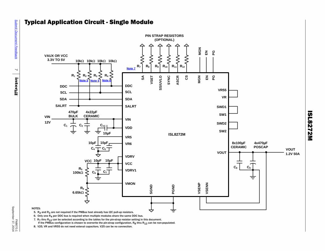
Typical Application Circuit - Single Module
VIN
VDD
VR55
VR5
VR
VOUTS
GN
D
PG
ND
VR6
VDRV
SCL
SDA
SALRT
VMON
VCC
VDRV1
VS
EN
P
VS
EN
N
VIN
VCC
ISL8272M
10µF
10µF 10µF S
A
VS
ET
EN
CS
SS
/UV
LO
AS
CR
VAUX OR VCC3.3V TO 5V
DDC
SY
NC
MG
N
SWD1
SW1
SWD2
SW2
12V
10µF
470µFBULK
4x22µFCERAMIC
8xCE
SCL
PIN STRAP RESISTORS (OPTIONAL)
EN
MG
N
SDA
SALRT
DDC
C1 C2 C3
C4 C5
C6 C7
10µF
C
R1 R2 R3 R4
R5
R6
R7 R8 R9 R10 R11 R12
PG
PG
10k 10k 10k 10k
100k
6.65k
NOTES:5. R2 and R3 are not required if the PMBus host already has I2C pull-up resistors.6. Only one R4 per DDC bus is required when multiple modules share the same DDC bus.7. R7 thru R12 can be selected according to the tables for the pin-strap resistor setting in this document.
If the PMBus configuration is chosen to overwrite the pin-strap configuration, R8 thru R12 can be non-populated.8. V25, VR and VR55 do not need extenal capacitors. V25 can be no connection.
Note 5 Note 5 Note 6
Note 7
ISL8272M
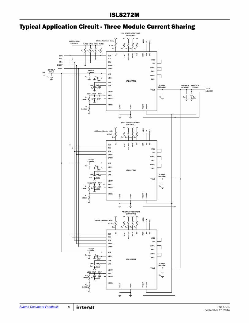
Typical Application Circuit - Three Module Current Sharing
VIN
VDD
VR55
VR5
VR
VOUT
SG
ND
PG
ND
VR6
VDRV
SCL
SDA
SALRT
VMON
VCC
VDRV1
VS
EN
P
VS
EN
N
VCC3
ISL8272M
10µF
10µF 10µF
SA
VS
ET
EN
CS
SS
/UV
LO
AS
CR
DDC
MG
N
SWD1
SW1
SWD2
SW210µF
4x22µFCERAMIC
4x100µFCERAMIC
PIN STRAP RESISTORS (OPTIONAL)
EN
MG
N
C16 C17
C18 C19
C20 C21
10µF
C22R19
R20
R21 R22 R23 R24 R25
PG
PG
3
VIN
VDD
VR55
VR5
VR
VOUT
SG
ND
PG
ND
VR6
VDRV
SCL
SDA
SALRT
VMON
VCC
VDRV1
VS
EN
P
VS
EN
N
VCC2
ISL8272M
10µF
10µF 10µF
SA
VS
ET
EN
CS
SS
/UV
LO
AS
CR
DDC
SYNC
MG
N
SWD1
SW1
SWD2
SW210µF
4x22µFCERAMIC
4x100µFCERAMIC
PIN STRAP RESISTORS (OPTIONAL)
EN
MG
N
C9 C10
C11 C12
C13 C14
10µF
C15R12
R13
R14 R16 R17 R18
PG
PG
2
VIN
VDD
VR55
VR5
VR
VOUT
SG
ND
PG
ND
VR6
VDRV
SCL
SDA
SALRT
VMON
VCC
VDRV1
VS
EN
P
VS
EN
N
VIN
VCC1
ISL8272M
VOUT
1.2V 150A
10µF
10µF 10µF
SA
VS
ET
EN
CS
SS
/UV
LO
AS
CR
VAUX or VCC3.3V to 5V
DDC
SYNC
MG
N
SWD1
SW1
SWD2
SW2
12V
10µF
2X470µFBULK
4x22µ FCERAMIC
4x100µFCERAMIC
12x470µ F POSCAP
SCL
PIN STRAP RESISTORS (OPTIONAL)
EN
MG
N
SDA
SALRT
DDC
C1 C2 C3
C4 C5
C6 C7
10µF
C8 C23
R1 R2 R3 R4
R5
R6
R7 R8 R9 R10 R11
PG
PG
1
SYNC
SYNC
12x100µ F CERAMIC
C24
R15
56.2k
SMBus Address = 0x2C
SMBus Address = 0x2B
SMBus Address= 0x2A
4.7k 4.7k 4.7k 4.7k
100k
6.65k
100k
6.65k
61.9k
100k
6.65k
51.1k
8 FN8670.1September 17, 2014
Submit Document Feedback
ISL8272M
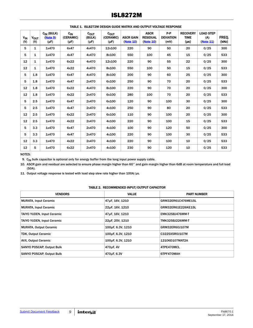
TABLE 1. ISL8272M DESIGN GUIDE MATRIX AND OUTPUT VOLTAGE RESPONSE
VIN (V)
VOUT (V)
CIN (BULK) (Note 9)
(µF)
CIN (CERAMIC)
(µF)
COUT(BULK)
(µF)
COUT (CERAMIC)
(µF)ASCR GAIN (Note 10)
ASCR RESIDUAL (Note 10)
P-P DEVIATION
(mV)
RECOVERY TIME (µs)
LOAD STEP (A)
(Note 11)FREQ. (kHz)
5 1 1x470 6x47 4x470 12x100 220 90 50 20 0/25 300
5 1 1x470 4x47 4x470 8x100 550 100 45 15 0/25 533
12 1 1x470 6x22 4x470 12x100 220 90 55 22 0/25 300
12 1 1x470 4x22 4x470 8x100 550 100 50 15 0/25 533
5 1.8 1x470 6x47 4x470 8x100 200 90 60 25 0/25 300
5 1.8 1x470 4x47 2x470 6x100 250 90 70 20 0/25 533
12 1.8 1x470 6x22 4x470 8x100 220 90 70 20 0/25 300
12 1.8 1x470 4x22 2x470 6x100 280 100 70 20 0/25 533
5 2.5 1x470 6x47 2x470 6x100 120 90 100 30 0/25 300
5 2.5 1x470 4x47 2x470 4x100 250 90 80 20 0/25 533
12 2.5 1x470 6x22 2x470 6x100 110 90 100 20 0/25 300
12 2.5 1x470 4x22 2x470 4x100 220 90 100 15 0/25 533
5 3.3 1x470 6x47 2x470 4x100 100 90 120 50 0/25 300
5 3.3 1x470 4x47 2x470 4x100 220 90 100 30 0/25 533
12 3.3 1x470 4x22 2x470 4x100 220 90 100 10 0/25 533
12 5 1x470 6x22 2x470 4x100 230 90 120 10 0/25 533
NOTES:
9. CIN bulk capacitor is optional only for energy buffer from the long input power supply cable.
10. ASCR gain and residual are selected to ensure phase margin higher than 60° and gain margin higher than 6dB at room temperature and full load (50A).
11. Output voltage response is tested with load step slew rate higher than 100A/µs.
TABLE 2. RECOMMENDED INPUT/OUTPUT CAPACITOR
VENDORS VALUE PART NUMBER
MURATA, Input Ceramic 47µF, 16V, 1210 GRM32ER61C476ME15L
MURATA, Input Ceramic 22µF, 16V, 1210 GRM32ER61E226KE15L
TAIYO YUDEN, Input Ceramic 47µF, 16V, 1210 EMK325BJ476MM-T
TAIYO YUDEN, Input Ceramic 22µF, 25V, 1210 TMK325BJ226MM-T
MURATA, Output Ceramic 100µF, 6.3V, 1210 GRM32ER60J107M
TDK, Output Ceramic 100µF, 6.3V, 1210 C3225X5R0J107M
AVX, Output Ceramic 100µF, 6.3V, 1210 12106D107MAT2A
SANYO POSCAP, Output Bulk 470µF, 4V 4TPE470MCL
SANYO POSCAP, Output Bulk 470µF, 6.3V 6TPF470MAH
9 FN8670.1September 17, 2014
Submit Document Feedback
ISL8272M
Absolute Maximum Ratings Thermal InformationInput Supply Voltage, VIN Pin . . . . . . . . . . . . . . . . . . . . . . . . . . . -0.3V to 17VInput Supply Voltage for Controller, VDD Pin . . . . . . . . . . . . . . -0.3V to 17VMOSFET Switch Node Voltage, SW1/2, SWD1/2. . . . . . . . . . . -0.3V to 17VMOSFET Driver Supply Voltage, VDRV, VDRV1 Pin . . . . . . . . . -0.3V to 6.0VOutput Voltage, VOUT pin. . . . . . . . . . . . . . . . . . . . . . . . . . . . . . .-0.3V to 6.0VInternal Reference Supply Voltage, VR6 Pin . . . . . . . . . . . . . . -0.3V to 6.6VInternal Reference Supply Voltage, VR, VR5, VR55 Pin. . . . . -0.3V to 6.5VInternal Reference Supply Voltage, V25 Pin . . . . . . . . . . . . . . . . -0.3V to 3VLogic I/O Voltage for DDC, EN, MGN, PG, ASCR, CS
SA, SCL, SDA, SALRT, SYNC, SS/UVLO, VMON, VSET . . . . . -0.3V to 6.0VAnalog Input Voltages for
VSENP . . . . . . . . . . . . . . . . . . . . . . . . . . . . . . . . . . . . . . . . . . . -0.3V to 6.0VVSENN . . . . . . . . . . . . . . . . . . . . . . . . . . . . . . . . . . . . . . . . . . . -0.3V to 0.3V
ESD RatingHuman Body Model (Tested per JESD22-A114F) . . . . . . . . . . . . . . 2000VMachine Model (Tested per JESD22-A115C) . . . . . . . . . . . . . . . . . . 200VCharged Device Model (Tested per JESD22-C110D) . . . . . . . . . . . . 750V
Latch-Up (Tested per JESD78C; Class 2, Level A) . . . . . . . . . . . . . . . 100mA
Thermal Resistance (Typical) JA (°C/W) JC (°C/W)58 LD HDA Package (Notes 12, 13). . . . . . 6.55 1.6
Maximum Junction Temperature (Plastic Package) . . . . . . . . . . . .+125°CStorage Temperature Range. . . . . . . . . . . . . . . . . . . . . . . .-55°C to +150°CPb-Free Reflow Profile . . . . . . . . . . . . . . . . . . . . . . . . . . . . . . . . . . see TB493
Recommended Operating ConditionsInput Supply Voltage Range, VIN . . . . . . . . . . . . . . . . . . . . . . . . 4.5V to 14VInput Supply Voltage Range for Controller, VDD . . . . . . . . . . . 4.5V to 14VOutput Voltage Range, VOUT . . . . . . . . . . . . . . . . . . . . . . . . . . . . .0.6V to 5VOutput Current Range, IOUT(DC) (Note 16). . . . . . . . . . . . . . . . . . . 0A to 50AOperating Junction Temperature Range, TJ. . . . . . . . . . . .-40°C to +125°C
CAUTION: Do not operate at or near the maximum ratings listed for extended periods of time. Exposure to such conditions may adversely impact productreliability and result in failures not covered by warranty.
NOTES:
12. JA is measured in free air with the module mounted on an 6-layer evaluation board 4.7x4.8inch in size with 2oz surface and 2oz buried planes and multiple via interconnects as specified in ISL8272MEVAL1Z Evaluation Board User Guide.
13. For JC, the “case temp” location is the center of the package underside.
Electrical Specifications VIN = VDD= 12V, fSW = 533kHz, TA = -40°C to +85°C, unless otherwise noted. Typical values are at TA = +25°C. Boldface limits apply across the operating temperature range, -40°C to +85°C.
SYMBOL PARAMETER TEST CONDITIONSMIN
(Note 14)TYP
MAX(Note 14)
UNITS
INPUT AND SUPPLY CHARACTERISTICS
IDD Input Supply Current for Controller VIN = VDD = 12V, VOUT = 0V, module not enabled
40 50 mA
VR6 6V Internal Reference Supply Voltage 5.5 6.1 6.6 V
VR5 5V Internal Reference Supply IVR5 <5mA 4.5 5.2 5.5 V
V25 2.5V Internal Reference Supply 2.25 2.5 2.75 V
Vcc Internal LDO Output Voltage 5.3 V
IVCC Internal LDO Output Current VIN = VDD = 12V, VCC connected to VDRV, module enabled
50 mA
VDD_READ_RES Input Supply Voltage for Controller Read Back Resolution
10 Bits
VDD_READ_ERR Input Supply Voltage for Controller Read Back Total Error (Note 17)
PMBus Read ±2 %FS
OUTPUT CHARACTERISTICS
VOUT_RANGE Output Voltage Adjustment Range VIN > VOUT + 1.8V 0.54 5.5 V
VOUT_RES Output Voltage Set-Point Range Configured using PMBus ±0.025 %
VOUT_ACCY Output Voltage Set-Point Accuracy (Notes 15, 17)
Includes line, load and temperature (-20°C ≤ TA ≤ +85°C)
-1 +1 % FS
VOUT_READ_RES Output Voltage Read back Resolution 10 Bits
VOUT_READ_ERR Output Voltage Read back Total Error (Note 17)
PMBus read -2 +2 % FS
IOUT_READ_RES Output Current Read back Resolution 10 Bits
10 FN8670.1September 17, 2014
Submit Document Feedback
ISL8272M
IOUT_RANGE Output Current Range (Note 16) 50 A
IOUT_READ_ERR Output Current Read back Total Error PMBus read at max load. VOUT = 1V ±3 A
SOFT-START AND SEQUENCING
tON_DELAY Delay Time From Enable to VOUT Rise Configured using PMBus 2 5000 ms
tON_DELAY_ACCY tON_DELAY Accuracy ±2 ms
tON_RISE Output Voltage Ramp-Up Time Configured using PMBus. Single module standalone
0.5 100 ms
tON_RISE_ACCY Output Voltage Ramp-Up Time Accuracy
Single module standalone ±250 µs
tOFF_DELAY Delay Time From disable to VOUT Fall Configured using PMBus 2 5000 ms
tOFF_DELAY_ACCY tOFF_DELAY Accuracy ±2 ms
tOFF_FALL Output Voltage Fall Time Configured using PMBus. Single module standalone
0.5 100 ms
tON_FALL_ACCY Output Voltage Fall Time Accuracy Single module standalone ±250 µs
POWER-GOOD
VPG_DELAY Power-Good Delay Configured using PMBus 0 5000 ms
TEMPERATURE SENSE
TSENSE_RANGE Temperature Sense Range Configurable via PMBus -50 150 C
INT_TEMPACCY Internal Temperature Sensor Accuracy Tested at +100°C -5 +5 C
FAULT PROTECTION
VDD_UVLO_RANGE VDD Undervoltage Threshold Range Measured internally 4.18 16 V
VDD_UVLO_ACCY VDD Undervoltage Threshold Accuracy (Note 17)
±2 %FS
VDD_UVLO_DELAY VDD Undervoltage Response Time 10 µs
VOUT_OV_RANGE VOUT Overvoltage Threshold Range Factory default 1.15VOUT V
Configured using PMBus 1.05VOUT VOUT_MAX V
VOUT_UV_RANGE VOUT Undervoltage Threshold Range Factory default 0.85VOUT V
Configured using PMBus 0 0.95VOUT V
VOUT_OV/UV_ACCY VOUT OV/UV Threshold Accuracy (Note 15)
-2 +2 %
VOUT_OV/UV_DELAY VOUT OV/UV Response Time 10 µs
ILIMIT_ACCY Output Current Limit Set-Point Accuracy (Note 17)
Tested at IOUT_OC_FAULT_LIMIT = 50A ±10 % FS
ILIMIT_DELAY Output Current Fault Response Time (Note 18)
Factory default 3 tSW
TJUNCTION Over-temperature Protection Threshold (Controller Junction Temperature)
Factory default 125 C
Configured using PMBus -40 125 C
TJUNCTION_HYS Thermal Protection Hysteresis 15 C
Electrical Specifications VIN = VDD= 12V, fSW = 533kHz, TA = -40°C to +85°C, unless otherwise noted. Typical values are at TA = +25°C. Boldface limits apply across the operating temperature range, -40°C to +85°C. (Continued)
SYMBOL PARAMETER TEST CONDITIONSMIN
(Note 14)TYP
MAX(Note 14)
UNITS
11 FN8670.1September 17, 2014
Submit Document Feedback
ISL8272M
OSCILLATOR AND SWITCHING CHARACTERISTICS
fSW_RANGE Switching Frequency Range 296 1067 kHz
fSW_ACCY Switching Frequency Set-point Accuracy
-5 +5 %
EXT_SYNCPW Minimum Pulse Width Required from External SYNC Clock
Measured at 50% Amplitude150 ns
EXT_SYNCDRIFT Drift Tolerance for External SYNC Clock External SYNC Clock equal to 500kHz is not supported
-10 +10 %
LOGIC INPUT/OUTPUT CHARACTERISTICS
ILOGIC_BIAS Bias Current at the Logic Input Pins DDC, EN, MGN, PG, SA, SCL, SDA, SALRT, SYNC, UVLO, VMON, VSET
-100 +100 nA
VLOGIC_IN_LOW Logic Input Low Threshold Voltage 0.8 V
VLOGIC_IN_HIGH Logic Input High Threshold Voltage 2.0 V
VLOGIC_OUT_LOW Logic Output Low Threshold Voltage 2mA sinking 0.5 V
VLOGIC_OUT_HIGH Logic Output High Threshold Voltage 2mA sourcing 2.25 V
PMBus INTERFACE TIMING CHARACTERISTIC
fSMB PMBus Operating Frequency 100 400 kHz
NOTES:
14. Compliance to datasheet limits is assured by one or more methods: Production test, characterization and/or design. Controller is independently tested before module assembly.
15. VOUT measured at the termination of the VSENP and VSENN sense points.
16. The MAX load current is determined by the thermal “Derating Curves” on page 15, provide with this document.
17. “FS” stand for full scale of recommended maximum operation range.
18. “tSW” stands for time period of operation switching frequency.
Electrical Specifications VIN = VDD= 12V, fSW = 533kHz, TA = -40°C to +85°C, unless otherwise noted. Typical values are at TA = +25°C. Boldface limits apply across the operating temperature range, -40°C to +85°C. (Continued)
SYMBOL PARAMETER TEST CONDITIONSMIN
(Note 14)TYP
MAX(Note 14)
UNITS
12 FN8670.1September 17, 2014
Submit Document Feedback
ISL8272M
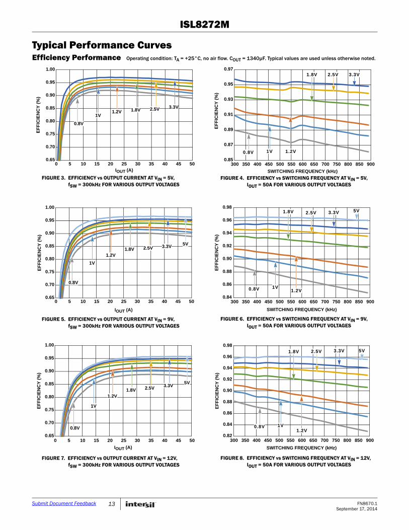
Typical Performance Curves Efficiency Performance Operating condition: TA = +25°C, no air flow. COUT = 1340µF. Typical values are used unless otherwise noted.
FIGURE 3. EFFICIENCY vs OUTPUT CURRENT AT VIN = 5V, fSW = 300kHz FOR VARIOUS OUTPUT VOLTAGES
FIGURE 4. EFFICIENCY vs SWITCHING FREQUENCY AT VIN = 5V, IOUT = 50A FOR VARIOUS OUTPUT VOLTAGES
FIGURE 5. EFFICIENCY vs OUTPUT CURRENT AT VIN = 9V, fSW = 300kHz FOR VARIOUS OUTPUT VOLTAGES
FIGURE 6. EFFICIENCY vs SWITCHING FREQUENCY AT VIN = 9V, IOUT = 50A FOR VARIOUS OUTPUT VOLTAGES
FIGURE 7. EFFICIENCY vs OUTPUT CURRENT AT VIN = 12V, fSW = 300kHz FOR VARIOUS OUTPUT VOLTAGES
FIGURE 8. EFFICIENCY vs SWITCHING FREQUENCY AT VIN = 12V, IOUT = 50A FOR VARIOUS OUTPUT VOLTAGES
0.65
0.70
0.75
0.80
0.85
0.90
0.95
1.00
0 5 10 15 20 25 30 35 40 45 50
0.8V
1V1.2V 1.8V 2.5V 3.3V
IOUT (A)
EF
FIC
IEN
CY
(%
)
0.85
0.87
0.89
0.91
0.93
0.95
0.97
300 350 400 450 500 550 600 650 700 750 800 850 900
SWITCHING FREQUENCY (kHz)
EF
FIC
IEN
CY
(%
)
1V 1.2V
1.8V 2.5V 3.3V
0.8V
0.65
0.70
0.75
0.80
0.85
0.90
0.95
1.00
0 5 10 15 20 25 30 35 40 45 50
0.8V
1V
1.2V1.8V 2.5V 3.3V
IOUT (A)
EF
FIC
IEN
CY
(%
)
5V
0.84
0.86
0.88
0.90
0.92
0.94
0.96
0.98
300 350 400 450 500 550 600 650 700 750 800 850 900
SWITCHING FREQUENCY (kHz)
EF
FIC
IEN
CY
(%
)
1V1.2V
1.8V 2.5V 3.3V
0.8V
5V
0.65
0.70
0.75
0.80
0.85
0.90
0.95
1.00
0 5 10 15 20 25 30 35 40 45 50
0.8V
1V
1.2V1.8V 2.5V 3.3V
IOUT (A)
EF
FIC
IEN
CY
(%
)
5V
0.82
0.84
0.86
0.88
0.90
0.92
0.94
0.96
0.98
300 350 400 450 500 550 600 650 700 750 800 850 900
SWITCHING FREQUENCY (kHz)
EF
FIC
IEN
CY
(%
)
1V1.2V
1.8V 2.5V 3.3V
0.8V
5V
13 FN8670.1September 17, 2014
Submit Document Feedback
ISL8272M
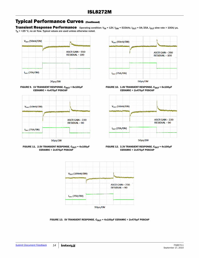
Transient Response Performance Operating condition: VIN = 12V, fSW = 533kHz, IOUT = 0A/25A, IOUT slew rate > 100A/µs, TA = +25°C, no air flow. Typical values are used unless otherwise noted.
FIGURE 9. 1V TRANSIENT RESPONSE. COUT = 8x100µF CERAMIC + 4x470µF POSCAP
FIGURE 10. 1.8V TRANSIENT RESPONSE. COUT = 6x100µF CERAMIC + 2x470µF POSCAP
FIGURE 11. 2.5V TRANSIENT RESPONSE. COUT = 4x100µF CERAMIC + 2x470µF POSCAP
FIGURE 12. 3.3V TRANSIENT RESPONSE. COUT = 4x100µF CERAMIC + 2x470µF POSCAP
FIGURE 13. 5V TRANSIENT RESPONSE. COUT = 4x100µF CERAMIC + 2x470µF POSCAP
Typical Performance Curves (Continued)
14 FN8670.1September 17, 2014
Submit Document Feedback
ISL8272M
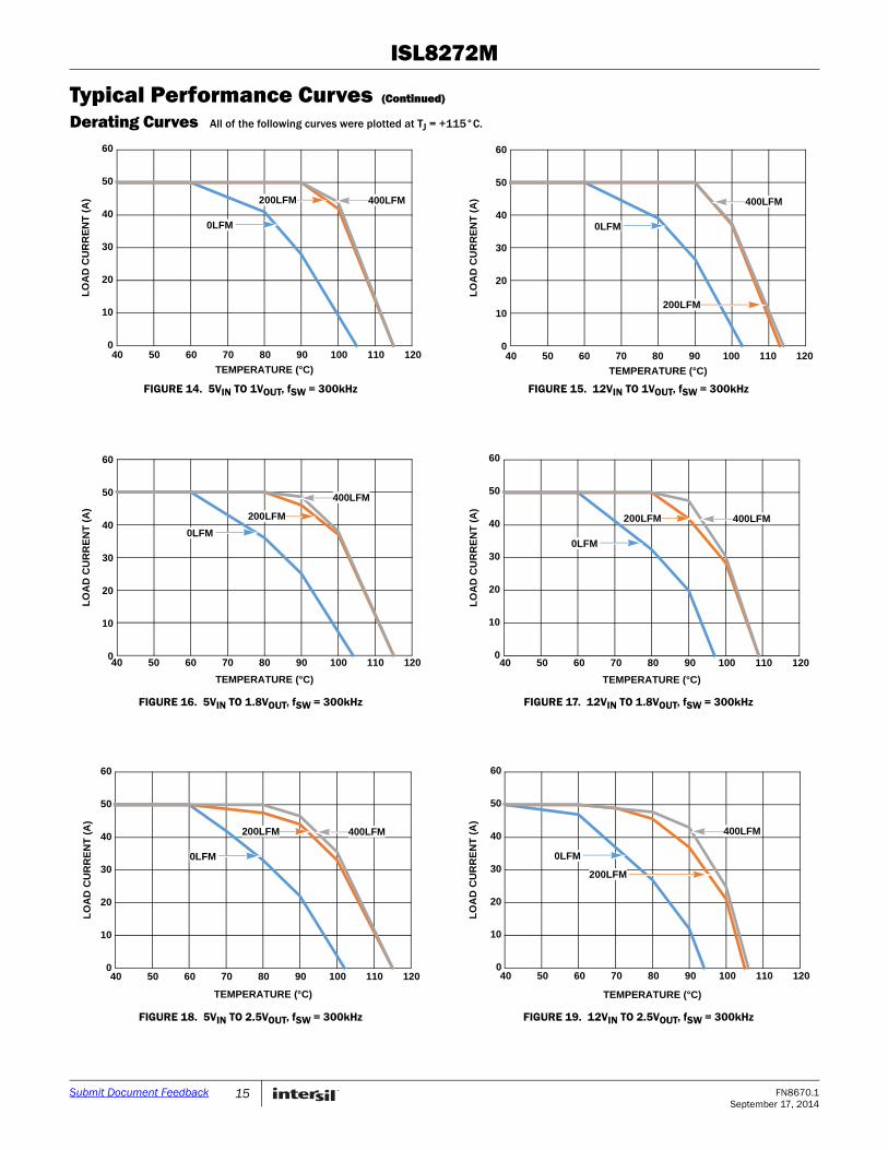
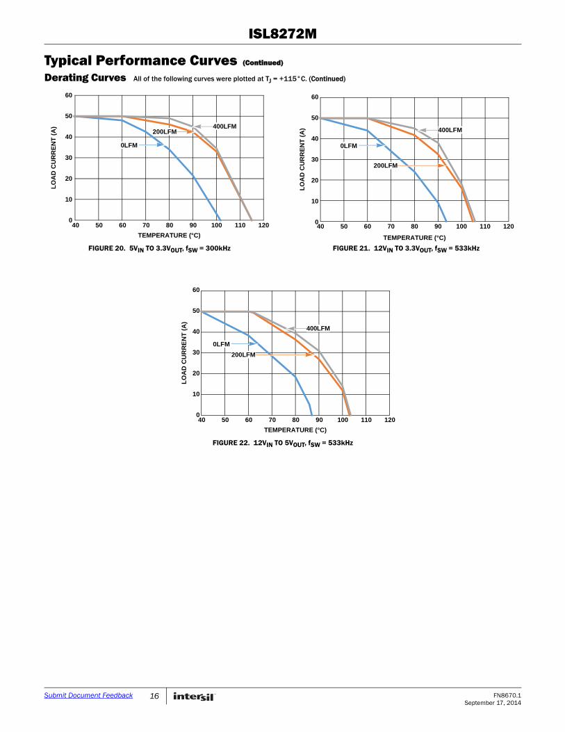
Derating Curves All of the following curves were plotted at TJ = +115°C.
FIGURE 14. 5VIN TO 1VOUT, fSW = 300kHz FIGURE 15. 12VIN TO 1VOUT, fSW = 300kHz
FIGURE 16. 5VIN TO 1.8VOUT, fSW = 300kHz FIGURE 17. 12VIN TO 1.8VOUT, fSW = 300kHz
FIGURE 18. 5VIN TO 2.5VOUT, fSW = 300kHz FIGURE 19. 12VIN TO 2.5VOUT, fSW = 300kHz
Typical Performance Curves (Continued)
0
10
20
30
40
50
60
40 50 60 70 80 90 100 110 120
TEMPERATURE (°C)
0LFM
200LFM 400LFM
LO
AD
CU
RR
EN
T (
A)
0
10
20
30
40
50
60
40 50 60 70 80 90 100 110 120
TEMPERATURE (°C)
0LFM
200LFM
400LFM
LO
AD
CU
RR
EN
T (
A)
40 50 60 70 80 90 100 110 120
TEMPERATURE (°C)
0LFM
200LFM
400LFM
LO
AD
CU
RR
EN
T (
A)
0
10
20
30
40
50
60
0
10
20
30
40
50
60
40 50 60 70 80 90 100 110 120
TEMPERATURE (°C)
0LFM
200LFM 400LFM
LO
AD
CU
RR
EN
T (
A)
0
10
20
30
40
50
60
40 50 60 70 80 90 100 110 120
TEMPERATURE (°C)
0LFM
200LFM 400LFM
LO
AD
CU
RR
EN
T (
A)
0
10
20
30
40
50
60
40 50 60 70 80 90 100 110 120
TEMPERATURE (°C)
0LFM
200LFM
400LFM
LO
AD
CU
RR
EN
T (
A)
15 FN8670.1September 17, 2014
Submit Document Feedback
ISL8272M
Derating Curves All of the following curves were plotted at TJ = +115°C. (Continued)
FIGURE 20. 5VIN TO 3.3VOUT, fSW = 300kHz FIGURE 21. 12VIN TO 3.3VOUT, fSW = 533kHz
FIGURE 22. 12VIN TO 5VOUT, fSW = 533kHz
Typical Performance Curves (Continued)
0
10
20
30
40
50
60
40 50 60 70 80 90 100 110 120
TEMPERATURE (°C)
0LFM
200LFM400LFM
LO
AD
CU
RR
EN
T (
A)
0
10
20
30
40
50
60
40 50 60 70 80 90 100 110 120
TEMPERATURE (°C)
0LFM
200LFM
400LFM
LO
AD
CU
RR
EN
T (
A)
0
10
20
30
40
50
60
40 50 60 70 80 90 100 110 120
TEMPERATURE (°C)
0LFM
200LFM
400LFM
LO
AD
CU
RR
EN
T (
A)
16 FN8670.1September 17, 2014
Submit Document Feedback
ISL8272M
Functional DescriptionSMBus CommunicationsThe ISL8272M provides a PMBus digital interface that enables the user to configure all aspects of the module operation as well as monitor the input and output parameters. The ISL8272M can be used with any SMBus host device. In addition, the module is compatible with PMBus™ Power System Management Protocol Specification Parts I and II version 1.2. The ISL8272M accepts most standard PMBus commands. When configuring the device with PMBus commands, it is recommended that the enable pin is tied to SGND.
The SMBus device address is the only parameter that must be set by external pins. All other device parameters can be set with PMBus commands.
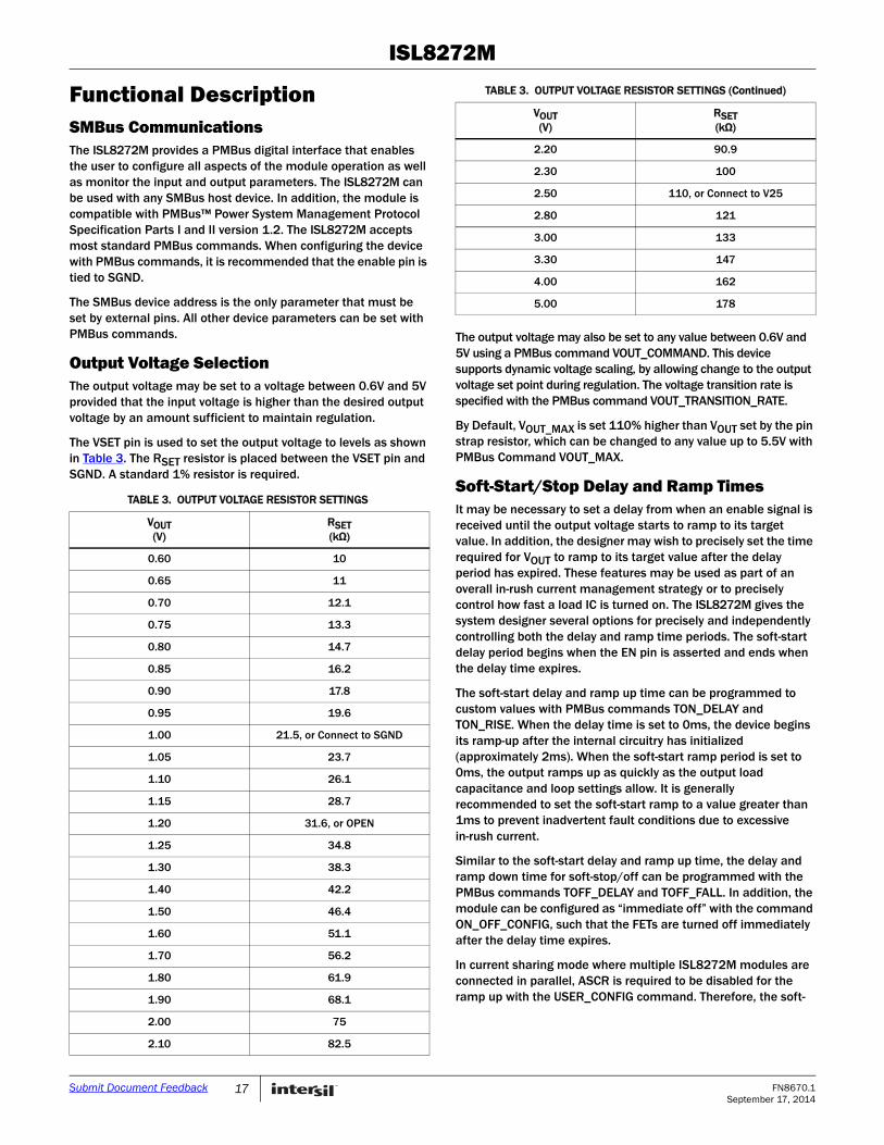
Output Voltage Selection The output voltage may be set to a voltage between 0.6V and 5V provided that the input voltage is higher than the desired output voltage by an amount sufficient to maintain regulation.
The VSET pin is used to set the output voltage to levels as shown in Table 3. The RSET resistor is placed between the VSET pin and SGND. A standard 1% resistor is required.
The output voltage may also be set to any value between 0.6V and 5V using a PMBus command VOUT_COMMAND. This device supports dynamic voltage scaling, by allowing change to the output voltage set point during regulation. The voltage transition rate is specified with the PMBus command VOUT_TRANSITION_RATE.
By Default, VOUT_MAX is set 110% higher than VOUT set by the pin strap resistor, which can be changed to any value up to 5.5V with PMBus Command VOUT_MAX.
Soft-Start/Stop Delay and Ramp TimesIt may be necessary to set a delay from when an enable signal is received until the output voltage starts to ramp to its target value. In addition, the designer may wish to precisely set the time required for VOUT to ramp to its target value after the delay period has expired. These features may be used as part of an overall in-rush current management strategy or to precisely control how fast a load IC is turned on. The ISL8272M gives the system designer several options for precisely and independently controlling both the delay and ramp time periods. The soft-start delay period begins when the EN pin is asserted and ends when the delay time expires.
The soft-start delay and ramp up time can be programmed to custom values with PMBus commands TON_DELAY and TON_RISE. When the delay time is set to 0ms, the device begins its ramp-up after the internal circuitry has initialized (approximately 2ms). When the soft-start ramp period is set to 0ms, the output ramps up as quickly as the output load capacitance and loop settings allow. It is generally recommended to set the soft-start ramp to a value greater than 1ms to prevent inadvertent fault conditions due to excessive in-rush current.
Similar to the soft-start delay and ramp up time, the delay and ramp down time for soft-stop/off can be programmed with the PMBus commands TOFF_DELAY and TOFF_FALL. In addition, the module can be configured as “immediate off” with the command ON_OFF_CONFIG, such that the FETs are turned off immediately after the delay time expires.
In current sharing mode where multiple ISL8272M modules are connected in parallel, ASCR is required to be disabled for the ramp up with the USER_CONFIG command. Therefore, the soft-
TABLE 3. OUTPUT VOLTAGE RESISTOR SETTINGS
VOUT (V)
RSET (kΩ)
0.60 10
0.65 11
0.70 12.1
0.75 13.3
0.80 14.7
0.85 16.2
0.90 17.8
0.95 19.6
1.00 21.5, or Connect to SGND
1.05 23.7
1.10 26.1
1.15 28.7
1.20 31.6, or OPEN
1.25 34.8
1.30 38.3
1.40 42.2
1.50 46.4
1.60 51.1
1.70 56.2
1.80 61.9
1.90 68.1
2.00 75
2.10 82.5
2.20 90.9
2.30 100
2.50 110, or Connect to V25
2.80 121
3.00 133
3.30 147
4.00 162
5.00 178
TABLE 3. OUTPUT VOLTAGE RESISTOR SETTINGS (Continued)
VOUT (V)
RSET (kΩ)
17 FN8670.1September 17, 2014
Submit Document Feedback
ISL8272M
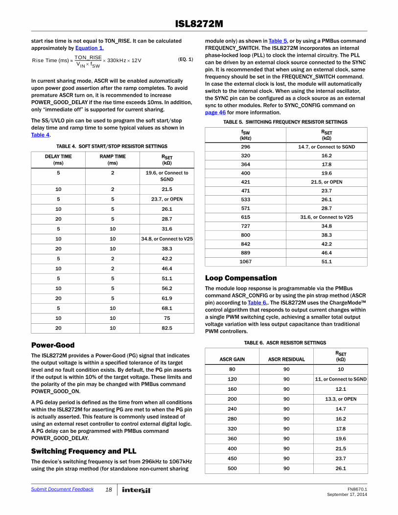
start rise time is not equal to TON_RISE. It can be calculated approximately by Equation 1.
In current sharing mode, ASCR will be enabled automatically upon power good assertion after the ramp completes. To avoid premature ASCR turn on, it is recommended to increase POWER_GOOD_DELAY if the rise time exceeds 10ms. In addition, only “immediate off” is supported for current sharing.
The SS/UVLO pin can be used to program the soft start/stop delay time and ramp time to some typical values as shown in Table 4.
Power-GoodThe ISL8272M provides a Power-Good (PG) signal that indicates the output voltage is within a specified tolerance of its target level and no fault condition exists. By default, the PG pin asserts if the output is within 10% of the target voltage. These limits and the polarity of the pin may be changed with PMBus command POWER_GOOD_ON.
A PG delay period is defined as the time from when all conditions within the ISL8272M for asserting PG are met to when the PG pin is actually asserted. This feature is commonly used instead of using an external reset controller to control external digital logic. A PG delay can be programmed with PMBus command POWER_GOOD_DELAY.
Switching Frequency and PLLThe device’s switching frequency is set from 296kHz to 1067kHz using the pin strap method (for standalone non-current sharing
module only) as shown in Table 5, or by using a PMBus command FREQUENCY_SWITCH. The ISL8272M incorporates an internal phase-locked loop (PLL) to clock the internal circuitry. The PLL can be driven by an external clock source connected to the SYNC pin. It is recommended that when using an external clock, same frequency should be set in the FREQUENCY_SWITCH command. In case the external clock is lost, the module will automatically switch to the internal clock. When using the internal oscillator, the SYNC pin can be configured as a clock source as an external sync to other modules. Refer to SYNC_CONFIG command on page 46 for more information.
Loop CompensationThe module loop response is programmable via the PMBus command ASCR_CONFIG or by using the pin strap method (ASCR pin) according to Table 6,. The ISL8272M uses the ChargeMode™ control algorithm that responds to output current changes within a single PWM switching cycle, achieving a smaller total output voltage variation with less output capacitance than traditional PWM controllers.
TABLE 4. SOFT START/STOP RESISTOR SETTINGS
DELAY TIME(ms)
RAMP TIME(ms)
RSET (kΩ)
5 2 19.6, or Connect to SGND
10 2 21.5
5 5 23.7, or OPEN
10 5 26.1
20 5 28.7
5 10 31.6
10 10 34.8, or Connect to V25
20 10 38.3
5 2 42.2
10 2 46.4
5 5 51.1
10 5 56.2
20 5 61.9
5 10 68.1
10 10 75
20 10 82.5
Rise Time (ms)TON_RISEVIN fSW
------------------------------- 330kHz 12V (EQ. 1)
TABLE 5. SWITCHING FREQUENCY RESISTOR SETTINGS
fSW (kHz)
RSET (kΩ)
296 14.7, or Connect to SGND
320 16.2
364 17.8
400 19.6
421 21.5, or OPEN
471 23.7
533 26.1
571 28.7
615 31.6, or Connect to V25
727 34.8
800 38.3
842 42.2
889 46.4
1067 51.1
TABLE 6. ASCR RESISTOR SETTINGS
ASCR GAIN ASCR RESIDUALRSET (kΩ)
80 90 10
120 90 11, or Connect to SGND
160 90 12.1
200 90 13.3, or OPEN
240 90 14.7
280 90 16.2
320 90 17.8
360 90 19.6
400 90 21.5
450 90 23.7
500 90 26.1
18 FN8670.1September 17, 2014
Submit Document Feedback
ISL8272M
Input Undervoltage Lockout (UVLO)The input undervoltage lockout (UVLO) prevents the ISL8272M from operating when the input falls below a preset threshold, indicating the input supply is out of its specified range. The UVLO threshold (VUVLO) can be set between 4.18V and 16V by using a PMBus command VIN_UV_FAULT_LIMIT. Using the pin strap method (SS/UVLO pin) as shown in Table 7 allows to set the VUVLO to two typical values.
Fault response to an input undervoltage fault can be programmed with PMBus command VIN_UV_FAULT_RESPONSE. If the input undervoltage fault retry is enabled, the module will shut down immediately once the input voltage falls below VUVLO, and then check the input voltage every 70ms. If the input voltage rises above the input undervoltage warning level, the module will restart. The input undervoltage warning is 1.05*VUVLO by default and can be programmed with the PMBus command VIN_UV_WARN_LIMIT.
SMBus Module Address SelectionEach module must have its own unique serial address to distinguish between other devices on the bus. The module address is set by connecting a resistor between the SA pin and SGND. Table 8 lists the available module addresses.
Output Overvoltage ProtectionThe ISL8272M offers an internal output overvoltage protection circuit that can be used to protect sensitive load circuitry from being subjected to a voltage higher than its prescribed limits. A hardware comparator is used to compare the actual output voltage (seen at the VSENP, VSENN pins) to a threshold set to 15% higher than the target output voltage (the default setting). Fault threshold can be programmed to a desired level with PMBus command VOUT_OV_FAULT_LIMIT. If the VSENP voltage exceeds this threshold, module will initiate an immediate shutdown without retry. 70ms continuous retry can be enabled with the PMBus command VOUT_OV_FAULT_RESPONSE.
550 90 28.7
600 90 31.6
700 90 34.8
800 90 38.3
80 100 42.2
120 100 46.4
160 100 51.1
200 100 56.2
240 100 61.9
280 100 68.1
320 100 75
360 100 82.5
400 100 90.9
450 100 100
500 100 110, or Connect to V25
550 100 121
600 100 133
700 100 147
800 100 162
TABLE 7. UVLO RESISTOR SETTINGS
UVLO (V)
RSET (kΩ)
4.5 OPEN
4.5 Connect to V25
4.5 Connect to SGND
4.5 19.6, 21.5, 23.7, 26.1, 28.7, 31.6, 34.8, 38.3
10.8 42.2, 46.4, 51.1, 56.2, 61.9, 68.1, 75, 82.5,
TABLE 6. ASCR RESISTOR SETTINGS (Continued)
ASCR GAIN ASCR RESIDUALRSET (kΩ)
TABLE 8. SMBus ADDRESS RESISTOR SELECTION
RSA (kΩ)
SMBus ADDRESS
10 19h
11 1Ah
12.1 1Bh
13.3 1Ch
14.7 1Dh
16.2 1Eh
17.8 1Fh
19.6 20h
21.5 21h
23.7 22h
26.1 23h
28.7 24h
31.6 25h
34.8, or connect to SGND 26h
38.3 27h
42.2, or Open 28h
46.4 29h
51.1 2Ah
56.2 2Bh
61.9 2Ch
68.1 2Dh
75 2Eh
82.5 2Fh
90.9 30h
100 31h
110 32h
121 33h
133 34h
147 35h
162 36h
178 37h
19 FN8670.1September 17, 2014
Submit Document Feedback
ISL8272M
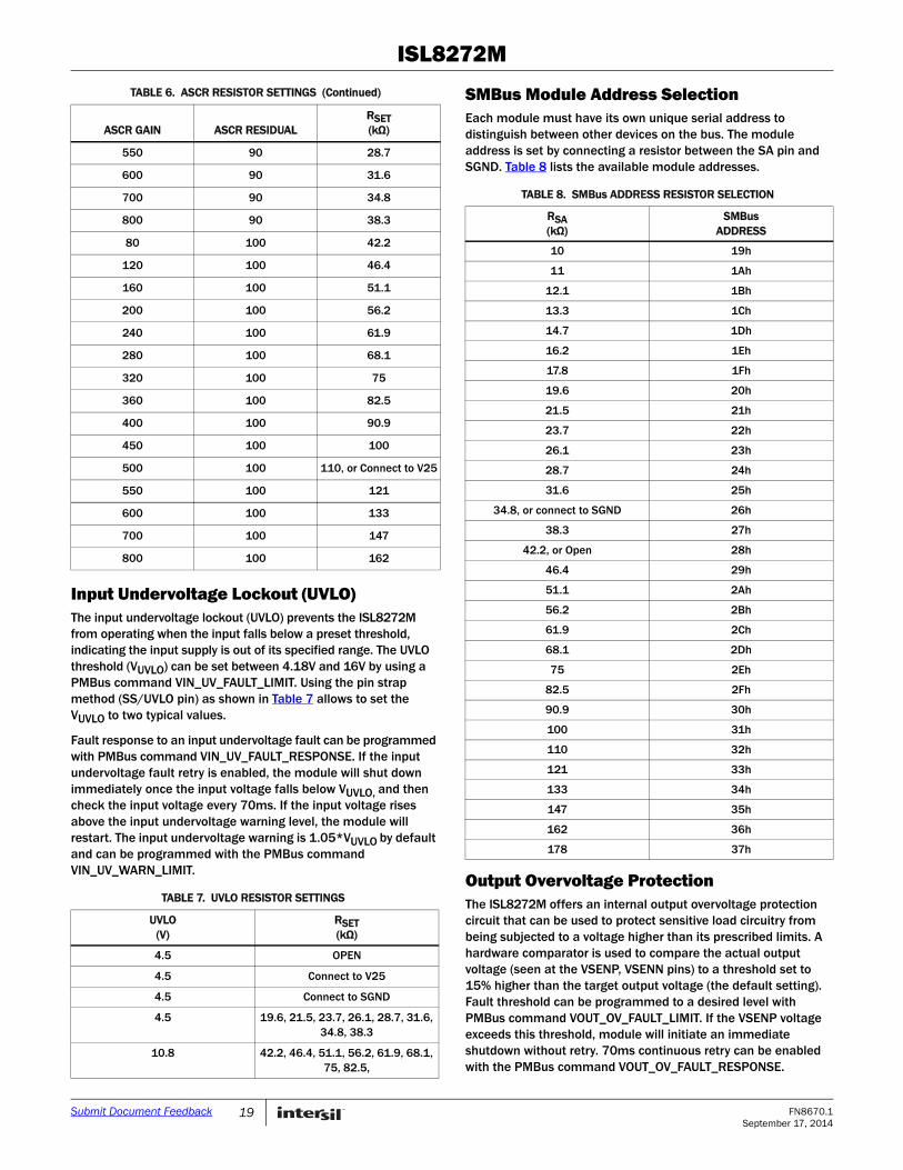
Internal to module, two 22Ω resistors are populated from VOUT to VSENP and SGND to VSENN to protect from overvoltage conditions in case of open at voltage sensing pins and differential remote sense traces due to assembly error. As long as differential remote sense traces have low resistance, VOUT regulation accuracy is not sacrificed.
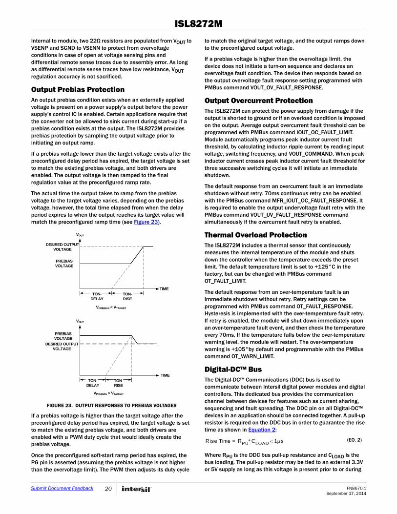
Output Prebias ProtectionAn output prebias condition exists when an externally applied voltage is present on a power supply’s output before the power supply’s control IC is enabled. Certain applications require that the converter not be allowed to sink current during start-up if a prebias condition exists at the output. The ISL8272M provides prebias protection by sampling the output voltage prior to initiating an output ramp.
If a prebias voltage lower than the target voltage exists after the preconfigured delay period has expired, the target voltage is set to match the existing prebias voltage, and both drivers are enabled. The output voltage is then ramped to the final regulation value at the preconfigured ramp rate.
The actual time the output takes to ramp from the prebias voltage to the target voltage varies, depending on the prebias voltage, however, the total time elapsed from when the delay period expires to when the output reaches its target value will match the preconfigured ramp time (see Figure 23).
If a prebias voltage is higher than the target voltage after the preconfigured delay period has expired, the target voltage is set to match the existing prebias voltage, and both drivers are enabled with a PWM duty cycle that would ideally create the prebias voltage.
Once the preconfigured soft-start ramp period has expired, the PG pin is asserted (assuming the prebias voltage is not higher than the overvoltage limit). The PWM then adjusts its duty cycle
to match the original target voltage, and the output ramps down to the preconfigured output voltage.
If a prebias voltage is higher than the overvoltage limit, the device does not initiate a turn-on sequence and declares an overvoltage fault condition. The device then responds based on the output overvoltage fault response setting programmed with PMBus command VOUT_OV_FAULT_RESPONSE.
Output Overcurrent ProtectionThe ISL8272M can protect the power supply from damage if the output is shorted to ground or if an overload condition is imposed on the output. Average output overcurrent fault threshold can be programmed with PMBus command IOUT_OC_FAULT_LIMIT. Module automatically programs peak inductor current fault threshold, by calculating inductor ripple current by reading input voltage, switching frequency, and VOUT_COMMAND. When peak inductor current crosses peak inductor current fault threshold for three successive switching cycles it will initiate an immediate shutdown.
The default response from an overcurrent fault is an immediate shutdown without retry. 70ms continuous retry can be enabled with the PMBus command MFR_IOUT_OC_FAULT_RESPONSE. It is required to enable the output undervoltage fault retry with the PMBus command VOUT_UV_FAULT_RESPONSE command simultaneously if the overcurrent fault retry is enabled.
Thermal Overload ProtectionThe ISL8272M includes a thermal sensor that continuously measures the internal temperature of the module and shuts down the controller when the temperature exceeds the preset limit. The default temperature limit is set to +125°C in the factory, but can be changed with PMBus command OT_FAULT_LIMIT.
The default response from an over-temperature fault is an immediate shutdown without retry. Retry settings can be programmed with PMBus command OT_FAULT_RESPONSE. Hysteresis is implemented with the over-temperature fault retry. If retry is enabled, the module will shut down immediately upon an over-temperature fault event, and then check the temperature every 70ms. If the temperature falls below the over-temperature warning level, the module will restart. The over-temperature warning is +105°by default and programmable with the PMBus command OT_WARN_LIMIT.
Digital-DC™ BusThe Digital-DC™ Communications (DDC) bus is used to communicate between Intersil digital power modules and digital controllers. This dedicated bus provides the communication channel between devices for features such as current sharing, sequencing and fault spreading. The DDC pin on all Digital-DC™ devices in an application should be connected together. A pull-up resistor is required on the DDC bus in order to guarantee the rise time as shown in Equation 2:
Where RPU is the DDC bus pull-up resistance and CLOAD is the bus loading. The pull-up resistor may be tied to an external 3.3V or 5V supply as long as this voltage is present prior to or during
FIGURE 23. OUTPUT RESPONSES TO PREBIAS VOLTAGES
DESIRED OUTPUT VOLTAGE
PREBIAS VOLTAGE
VOUT
TIME
TON- DELAY
TON-RISE
DESIRED OUTPUT VOLTAGE
PREBIAS VOLTAGE
VOUT
TIME
VPREBIAS < VTARGET
VPREBIAS > VTARGET
TON-RISE
TON- DELAY
Rise Time RPUCLOAD 1s= (EQ. 2)
20 FN8670.1September 17, 2014
Submit Document Feedback
ISL8272M
device power-up. In principle, each device connected to the DDC bus presents approximately 10pF of capacitive loading, and each inch of FR4 PCB trace introduces approximately 2pF. The ideal design uses a central pull-up resistor that is well-matched to the total load capacitance.
Active Current SharingParalleling multiple ISL8272M modules can be used to increase the output current capability of a single power rail. By connecting the DDC and SYNC pins of each module together and configuring the modules as a current sharing rail, the units will share the current equally within a few percent.
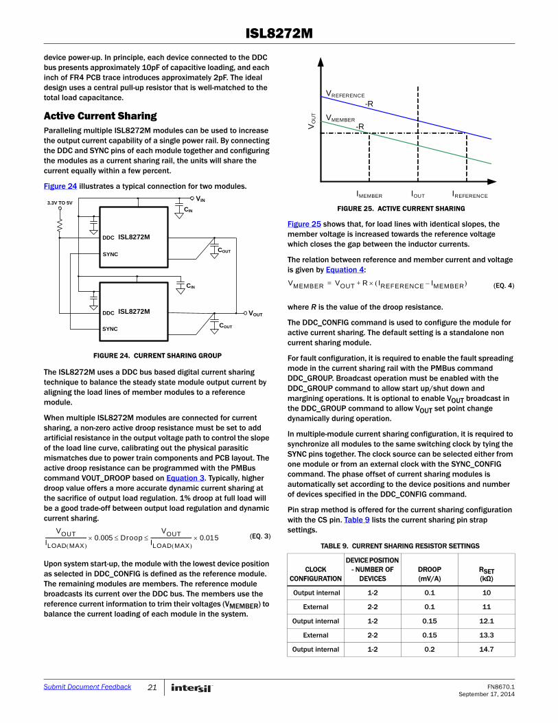
Figure 24 illustrates a typical connection for two modules.
The ISL8272M uses a DDC bus based digital current sharing technique to balance the steady state module output current by aligning the load lines of member modules to a reference module.
When multiple ISL8272M modules are connected for current sharing, a non-zero active droop resistance must be set to add artificial resistance in the output voltage path to control the slope of the load line curve, calibrating out the physical parasitic mismatches due to power train components and PCB layout. The active droop resistance can be programmed with the PMBus command VOUT_DROOP based on Equation 3. Typically, higher droop value offers a more accurate dynamic current sharing at the sacrifice of output load regulation. 1% droop at full load will be a good trade-off between output load regulation and dynamic current sharing.
Upon system start-up, the module with the lowest device position as selected in DDC_CONFIG is defined as the reference module. The remaining modules are members. The reference module broadcasts its current over the DDC bus. The members use the reference current information to trim their voltages (VMEMBER) to balance the current loading of each module in the system.
Figure 25 shows that, for load lines with identical slopes, the member voltage is increased towards the reference voltage which closes the gap between the inductor currents.
The relation between reference and member current and voltage is given by Equation 4:
where R is the value of the droop resistance.
The DDC_CONFIG command is used to configure the module for active current sharing. The default setting is a standalone non current sharing module.
For fault configuration, it is required to enable the fault spreading mode in the current sharing rail with the PMBus command DDC_GROUP. Broadcast operation must be enabled with the DDC_GROUP command to allow start up/shut down and margining operations. It is optional to enable VOUT broadcast in the DDC_GROUP command to allow VOUT set point change dynamically during operation.
In multiple-module current sharing configuration, it is required to synchronize all modules to the same switching clock by tying the SYNC pins together. The clock source can be selected either from one module or from an external clock with the SYNC_CONFIG command. The phase offset of current sharing modules is automatically set according to the device positions and number of devices specified in the DDC_CONFIG command.
Pin strap method is offered for the current sharing configuration with the CS pin. Table 9 lists the current sharing pin strap settings.
ISL8272M
VOUTISL8272M
VIN
COUT
CIN
COUT
CIN
DDC
DDC
3.3V TO 5V
SYNC
SYNC
FIGURE 24. CURRENT SHARING GROUP
VOUTILOAD MAX ---------------------------------- 0.005 Droop
VOUTILOAD MAX ---------------------------------- 0.01 5 (EQ. 3)
TABLE 9. CURRENT SHARING RESISTOR SETTINGS
CLOCK CONFIGURATION
DEVICE POSITION - NUMBER OF
DEVICESDROOP (mV/A)
RSET(kΩ)
Output internal 1-2 0.1 10
External 2-2 0.1 11
Output internal 1-2 0.15 12.1
External 2-2 0.15 13.3
Output internal 1-2 0.2 14.7
-R
-R
VREFERENCE
VMEMBER
IMEMBER IREFERENCEIOUT
VO
UT
FIGURE 25. ACTIVE CURRENT SHARING
(EQ. 4)VMEMBER VOUT R IREFERENCE IMEMBER– +=
21 FN8670.1September 17, 2014
Submit Document Feedback
ISL8272M
Phase SpreadingWhen multiple point-of-load converters share a common DC input supply, it is desirable to adjust the clock phase offset of each device, such that not all devices start to switch simultaneously. Setting each converter to start its switching cycle at a different point in time, can dramatically reduce input capacitance requirements and efficiency losses. Since the peak current drawn from the input supply is effectively spread out over a period of time, the peak current drawn at any given moment is reduced, and the power losses proportional to the IRMS
2 are reduced dramatically.
To enable phase spreading, all converters must be synchronized to the same switching clock. The phase offset of each device may also be set to any value between 0° and 360° in 22.5° increments with the PMBus command INTERLEAVE. The internal two phases of the module always maintain a phase difference of 180°.
Fault SpreadingDigital-DC modules and devices can be configured to broadcast a fault event over the DDC bus to the other devices in the group with PMBus command DDC_GROUP. When a nondestructive fault occurs, the device shuts down and broadcasts the fault event over the DDC bus. The other devices on the DDC bus shutdown simultaneously, if configured to do so, and attempt to restart.
Output SequencingA group of Digital-DC modules or devices may be configured to power-up in a predetermined sequence. This feature is especially useful when powering advanced processors (FPGAs and ASICs) that require one supply to reach its operating voltage prior to another supply reaching its operating voltage in order to avoid latch-up. Multi-device sequencing can be achieved by configuring each device with PMBus command SEQUENCE. Multiple device sequencing is configured by issuing PMBus commands to assign the preceding device in the sequencing chain as well as the device that follows in the sequencing chain.
The Enable pins of all devices in a sequencing group must be tied together and driven high to initiate a sequenced turn-on of the group. Enable must be driven low to initiate a sequenced turnoff of the group. It is recommend to enable fault spreading with the PMBus command DDC_GROUP within a sequencing group.
Monitoring Via SMBusA system controller can monitor a wide variety of different ISL8272M system parameters with PMBus commands:
• READ_VIN
• READ_VOUT
• READ_IOUT
• READ_INTERNAL_TEMP
• READ_DUTY_CYCLE
• READ_FREQEUNCY
• READ_VMON
Snapshot Parameter CaptureThe ISL8272M offers a special feature to capture parametric data and some fault status following a fault. Detail description is provided in “PMBus Commands Description” on page 29 under PMBus command SNAPSHOT and SNAPSHOT_CONTROL.
Nonvolatile Memory The ISL8272M has internal nonvolatile memory where user configurations are stored. Integrated security measures ensure that the user can only restore the module to a level that has been made available to them. During the initialization process, the ISL8272M checks for stored values contained in its internal non-volatile memory.
Modules are shipped with factory defaults configuration and most settings can be overwritten with PMBus Commands and can be stored in nonvolatile memory with PMBus command STORE_USER_ALL.
External 2-2 0.2 16.2
Output internal 1-2 0.25 17.8
External 2-2 0.25 19.6
Output internal 1-2 0.3 21.5
External 2-2 0.3 23.7
Output internal 1-3 0.07 26.1
External 2-3 0.07 28.7
External 3-3 0.07 31.6
Output internal 1-3 0.1 34.8
External 2-3 0.1 38.3
External 3-3 0.1 42.2
Output internal 1-3 0.13 46.4
External 2-3 0.13 51.1
External 3-3 0.13 56.2
Output internal 1-3 0.16 61.9
External 2-3 0.16 68.1
External 3-3 0.16 75
Output internal 1-3 0.2 82.5
External 2-3 0.2 90.9
External 3-3 0.2 100
Internal only 1-1 0 Connect to SGND (for immediate
off)
Internal only 1-1 0 OPEN (for soft off)
TABLE 9. CURRENT SHARING RESISTOR SETTINGS (Continued)
CLOCK CONFIGURATION
DEVICE POSITION - NUMBER OF
DEVICESDROOP (mV/A)
RSET(kΩ)
22 FN8670.1September 17, 2014
Submit Document Feedback
ISL8272M
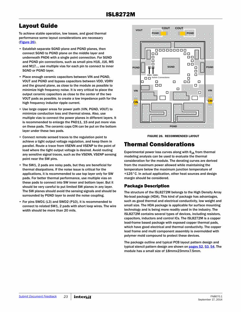
Layout GuideTo achieve stable operation, low losses, and good thermal performance some layout considerations are necessary (Figure 26).
• Establish separate SGND plane and PGND planes, then connect SGND to PGND plane on the middle layer and underneath PAD6 with a single point connection. For SGND and PGND pin connections, such as small pins H16, J16, M5 and M17..., use multiple vias for each pin to connect to inner SGND or PGND layer.
• Place enough ceramic capacitors between VIN and PGND, VOUT and PGND and bypass capacitors between VDD, VDRV and the ground plane, as close to the module as possible to minimize high frequency noise. It is very critical to place the output ceramic capacitors as close to the center of the two VOUT pads as possible, to create a low impedance path for the high frequency inductor ripple current.
• Use large copper areas for power path (VIN, PGND, VOUT) to minimize conduction loss and thermal stress. Also, use multiple vias to connect the power planes in different layers. It is recommended to enlarge the PAD11, 15 and put more vias on these pads. The ceramic caps CIN can be put on the bottom layer under these two pads.
• Connect remote sensed traces to the regulation point to achieve a tight output voltage regulation, and keep them in parallel. Route a trace from VSENN and VSENP to the point of load where the tight output voltage is desired. Avoid routing any sensitive signal traces, such as the VSENN, VSENP sensing point near the SW pins.
• The SW1, 2 pads are noisy pads, but they are beneficial for thermal dissipations. If the noise issue is critical for the applications, it is recommended to use top layer only for SW pads. For better thermal performance, use multiple vias on these pads to connect into SW inner and bottom layer. But it should be very careful to put limited SW planes in any layer. The SW planes should avoid the sensing signals and should be surrounded by PGND layer to avoid the noise coupling.
• For pins SWD1 (L3) and SWD2 (P10), it is recommended to connect to related SW1, 2 pads with short loop wires. The wire width should be more than 20 mils.
Thermal ConsiderationsExperimental power loss curves along with θJA from thermal modeling analysis can be used to evaluate the thermal consideration for the module. The derating curves are derived from the maximum power allowed while maintaining the temperature below the maximum junction temperature of +125°C. In actual application, other heat sources and design margin should be considered.
Package Description The structure of the ISL8272M belongs to the High Density Array No-lead package (HDA). This kind of package has advantages, such as good thermal and electrical conductivity, low weight and small size. The HDA package is applicable for surface mounting technology and is being more readily used in the industry. The ISL8272M contains several types of devices, including resistors, capacitors, inductors and control ICs. The ISL8272M is a copper lead-frame based package with exposed copper thermal pads, which have good electrical and thermal conductivity. The copper lead frame and multi component assembly is overmolded with polymer mold compound to protect these devices.
The package outline and typical PCB layout pattern design and typical stencil pattern design are shown on pages 52, 53, 54. The module has a small size of 18mmx23mmx7.5mm.
FIGURE 26. RECOMMENDED LAYOUT
PGND
VIN VIN
PGND PGND
VOUT
SGND
VSEN+VSEN-
Kelvin Connections
CIN CIN
PGND PGND
COUT COUT
23 FN8670.1September 17, 2014
Submit Document Feedback
ISL8272M
PCB Layout Pattern DesignThe bottom of ISL8272M is a lead-frame footprint, which is attached to the PCB by surface mounting process. The PCB layout pattern is shown on page 54. The PCB layout pattern is essentially 1:1 with the HDA exposed pad and I/O termination dimensions. The thermal lands on the PCB layout should match 1:1 with the package exposed die pads.
Thermal ViasA grid of 1.0mm to 1.2mm pitch thermal vias, which drops down and connects to buried copper plane(s), should be placed under the thermal land. The vias should be about 0.3mm to 0.33mm in diameter with the barrel plated to about 1.0 ounce copper. Although adding more vias (by decreasing via pitch) will improve the thermal performance, diminishing returns will be seen as more and more vias are added. Simply use as many vias as practical for the thermal land size and your board design rules allow.
Stencil Pattern DesignReflowed solder joints on the perimeter I/O lands should have about a 50µm to 75µm (2mil to 3mil) standoff height. The solder paste stencil design is the first step in developing optimized, reliable solder joins. Stencil aperture size to land size ratio should typically be 1:1. The aperture width may be reduced slightly to help prevent solder bridging between adjacent I/O lands. To reduce solder paste volume on the larger thermal lands, it is recommended that an array of smaller apertures be used instead of one large aperture. It is recommended that the stencil printing area cover 50% to 80% of the PCB layout pattern. A typical solder stencil pattern is shown on page 53. The gap width between pad to pad is 0.6mm. The user should consider the symmetry of the whole stencil pattern when designing its pads. A laser cut, stainless steel stencil with electropolished trapezoidal walls is recommended. Electropolishing “smooths” the aperture walls
resulting in reduced surface friction and better paste release which reduces voids. Using a Trapezoidal Section Aperture (TSA) also promotes paste release and forms a “brick like” paste deposit that assists in firm component placement. A 0.1mm to 0.15mm stencil thickness is recommended for this large pitch (1.3mm) HDA.
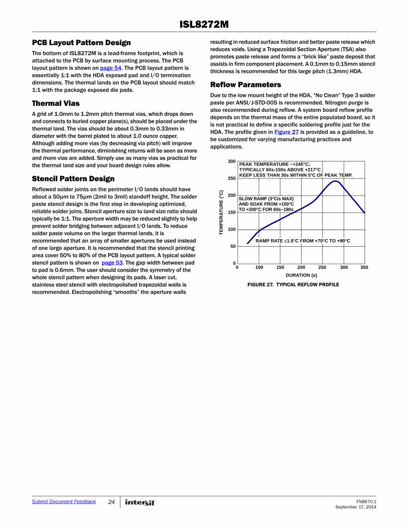
Reflow ParametersDue to the low mount height of the HDA, “No Clean” Type 3 solder paste per ANSI/J-STD-005 is recommended. Nitrogen purge is also recommended during reflow. A system board reflow profile depends on the thermal mass of the entire populated board, so it is not practical to define a specific soldering profile just for the HDA. The profile given in Figure 27 is provided as a guideline, to be customized for varying manufacturing practices and applications.
FIGURE 27. TYPICAL REFLOW PROFILE
0 300100 150 200 250 3500
50
100
150
200
250
300
TE
MP
ER
AT
UR
E (
°C)
DURATION (s)
SLOW RAMP (3°C/s MAX)AND SOAK FROM +150°CTO +200°C FOR 60s~180s
RAMP RATE 1.5°C FROM +70°C TO +90°C
PEAK TEMPERATURE ~+245°C; TYPICALLY 60s-150s ABOVE +217°CKEEP LESS THAN 30s WITHIN 5°C OF PEAK TEMP.
24 FN8670.1September 17, 2014
Submit Document Feedback
ISL8272M
PMBus Command SummaryCOMMAND
CODECOMMAND
NAME DESCRIPTION TYPEDATA
FORMATDEFAULT
VALUEDEFAULT SETTING PAGE
01h OPERATION Sets Enable, Disable and VOUT Margin modes.
R/W BYTE BIT 29
02h ON_OFF_CONFIG Configures the EN pin and PMBus commands to turn the unit ON/OFF
R/W BYTE BIT 16h Hardware Enable, Soft Off
29
03h CLEAR_FAULTS Clears fault indications. SEND BYTE 29
15h STORE_USER_ALL Stores all PMBus values written since last restore at user level.
SEND BYTE 29
16h RESTORE_USER_ALL Restores PMBus settings that were stored using STORE_USER_ALL.
SEND BYTE 30
20h VOUT_MODE Preset to defined data format of VOUT commands.
READ BYTE BIT 13h Linear Mode, Exponent = -13
30
21h VOUT_COMMAND Sets the nominal value of the output voltage.
R/W WORD L16u Pin Strap 30
23h VOUT_CAL_OFFSET Applies a fixed offset voltage to the VOUT_COMMAND.
R/W WORD L16s 0000h 0V 30
24h VOUT_MAX Sets the maximum possible value of VOUT. 110% of pin strap VOUT.
R/W WORD L16u 1.1*VOUT Pin Strap
30
25h VOUT_MARGIN_HIGH Sets the value of the VOUT during a margin high.
R/W WORD L16u 1.05*VOUT Pin Strap
30
26h VOUT_MARGIN_LOW Sets the value of the VOUT during a margin low.
R/W WORD L16u 0.95*VOUT Pin Strap
31
27h VOUT_TRANSITION_RATE Sets the transition rate during margin or other change of VOUT.
R/W WORD L11 BA00h 1V/ms 31
28h VOUT_DROOP Sets the loadline (V/I Slope) resistance for the rail.
R/W WORD L11 Pin Strap 31
33h FREQUENCY_SWITCH Sets the switching frequency. R/W WORD L11 Pin Strap 31
37h INTERLEAVE Configures a phase offset between devices sharing a SYNC clock.
R/W WORD BIT 0000h 31
38h IOUT_CAL_GAIN Sense resistance for inductor DCR current sensing.
R/W WORD L11 B370h 0.86mΩ 32
39h IOUT_CAL_OFFSET Sets the current-sense offset. R/W WORD L11 0000h 0A 32
40h VOUT_OV_FAULT_LIMIT Sets the VOUT overvoltage fault threshold.
R/W WORD L16u 1.15*VOUT Pin Strap
32
41h VOUT_OV_FAULT_RESPONSE Configures the VOUT overvoltage fault response.
R/W BYTE BIT 80h Disable andNo Retry
32
42h VOUT_OV_WARN_LIMIT Sets the VOUT overvoltage warn threshold.
R/W WORD L16u 1.10*VOUT Pin Strap
32
43h VOUT_UV_WARN_LIMIT Sets the VOUT undervoltage warn threshold.
R/W WORD L16u 0.9 * VOUT Pin Strap
32
44h VOUT_UV_FAULT_LIMIT Sets the VOUT undervoltage fault threshold.
R/W WORD L16u 0.85*VOUT Pin Strap
33
45h VOUT_UV_FAULT_RESPONSE Configures the VOUT undervoltage fault response.
R/W BYTE BIT 80h Disable andNo Retry
33
46h IOUT_OC_FAULT_LIMIT Sets the IOUT average overcurrent fault threshold.
R/W WORD L11 E3C0h 60A 33
4Bh IOUT_UC_FAULT_LIMIT Sets the IOUT average undercurrent fault threshold.
R/W WORD L11 E440h -60A 33
4Fh OT_FAULT_LIMIT Sets the over-temperature fault threshold.
R/W WORD L11 EBE8h +125°C 33
50h OT_FAULT_RESPONSE Configures the over-temperature fault response.
R/W BYTE BIT 80h Disable andNo Retry
34
25 FN8670.1September 17, 2014
Submit Document Feedback
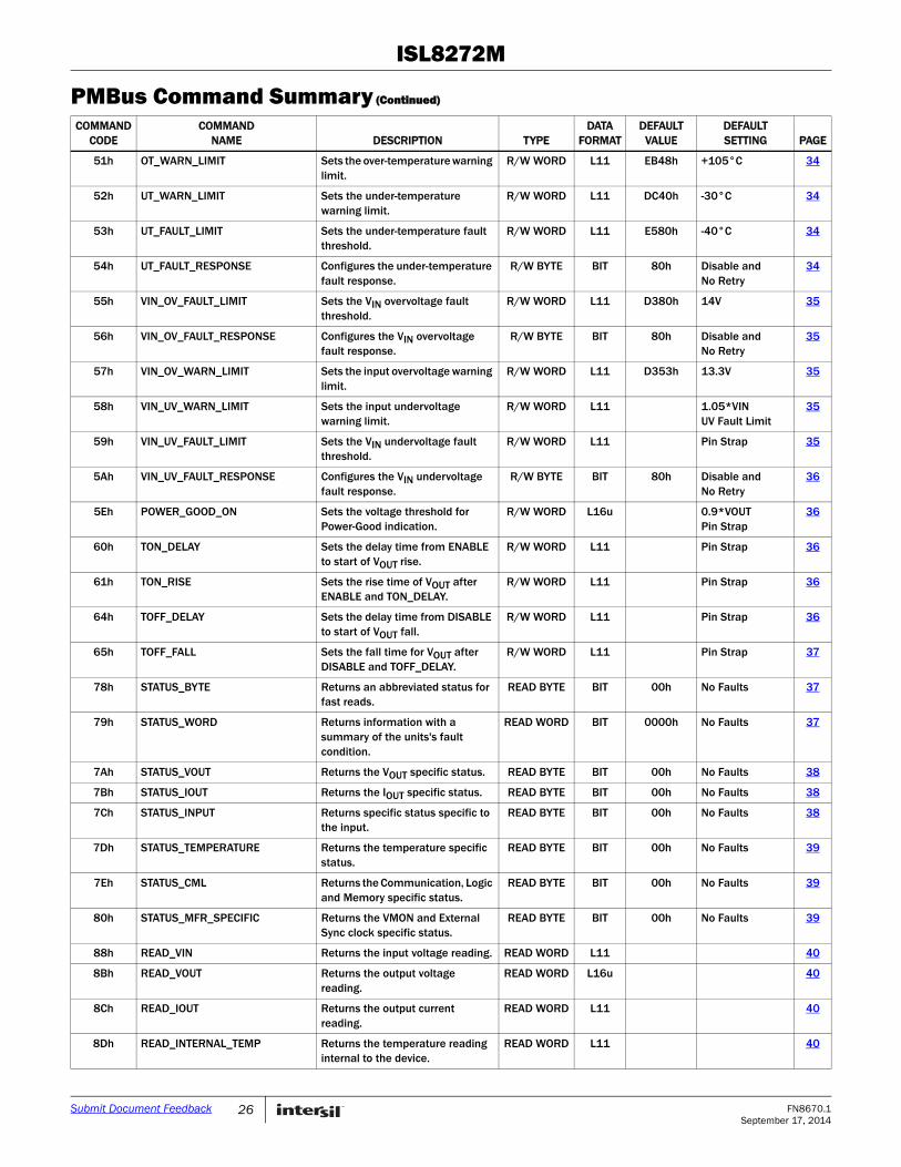
ISL8272M
51h OT_WARN_LIMIT Sets the over-temperature warning limit.
R/W WORD L11 EB48h +105°C 34
52h UT_WARN_LIMIT Sets the under-temperature warning limit.
R/W WORD L11 DC40h -30°C 34
53h UT_FAULT_LIMIT Sets the under-temperature fault threshold.
R/W WORD L11 E580h -40°C 34
54h UT_FAULT_RESPONSE Configures the under-temperature fault response.
R/W BYTE BIT 80h Disable andNo Retry
34
55h VIN_OV_FAULT_LIMIT Sets the VIN overvoltage fault threshold.
R/W WORD L11 D380h 14V 35
56h VIN_OV_FAULT_RESPONSE Configures the VIN overvoltage fault response.
R/W BYTE BIT 80h Disable andNo Retry
35
57h VIN_OV_WARN_LIMIT Sets the input overvoltage warning limit.
R/W WORD L11 D353h 13.3V 35
58h VIN_UV_WARN_LIMIT Sets the input undervoltage warning limit.
R/W WORD L11 1.05*VIN UV Fault Limit
35
59h VIN_UV_FAULT_LIMIT Sets the VIN undervoltage fault threshold.
R/W WORD L11 Pin Strap 35
5Ah VIN_UV_FAULT_RESPONSE Configures the VIN undervoltage fault response.
R/W BYTE BIT 80h Disable andNo Retry
36
5Eh POWER_GOOD_ON Sets the voltage threshold for Power-Good indication.
R/W WORD L16u 0.9*VOUT Pin Strap
36
60h TON_DELAY Sets the delay time from ENABLE to start of VOUT rise.
R/W WORD L11 Pin Strap 36
61h TON_RISE Sets the rise time of VOUT after ENABLE and TON_DELAY.
R/W WORD L11 Pin Strap 36
64h TOFF_DELAY Sets the delay time from DISABLE to start of VOUT fall.
R/W WORD L11 Pin Strap 36
65h TOFF_FALL Sets the fall time for VOUT after DISABLE and TOFF_DELAY.
R/W WORD L11 Pin Strap 37
78h STATUS_BYTE Returns an abbreviated status for fast reads.
READ BYTE BIT 00h No Faults 37
79h STATUS_WORD Returns information with a summary of the units's fault condition.
READ WORD BIT 0000h No Faults 37
7Ah STATUS_VOUT Returns the VOUT specific status. READ BYTE BIT 00h No Faults 38
7Bh STATUS_IOUT Returns the IOUT specific status. READ BYTE BIT 00h No Faults 38
7Ch STATUS_INPUT Returns specific status specific to the input.
READ BYTE BIT 00h No Faults 38
7Dh STATUS_TEMPERATURE Returns the temperature specific status.
READ BYTE BIT 00h No Faults 39
7Eh STATUS_CML Returns the Communication, Logic and Memory specific status.
READ BYTE BIT 00h No Faults 39
80h STATUS_MFR_SPECIFIC Returns the VMON and External Sync clock specific status.
READ BYTE BIT 00h No Faults 39
88h READ_VIN Returns the input voltage reading. READ WORD L11 40
8Bh READ_VOUT Returns the output voltage reading.
READ WORD L16u 40
8Ch READ_IOUT Returns the output current reading.
READ WORD L11 40
8Dh READ_INTERNAL_TEMP Returns the temperature reading internal to the device.
READ WORD L11 40
PMBus Command Summary (Continued)
COMMAND CODE
COMMAND NAME DESCRIPTION TYPE
DATAFORMAT
DEFAULT VALUE
DEFAULT SETTING PAGE
26 FN8670.1September 17, 2014
Submit Document Feedback
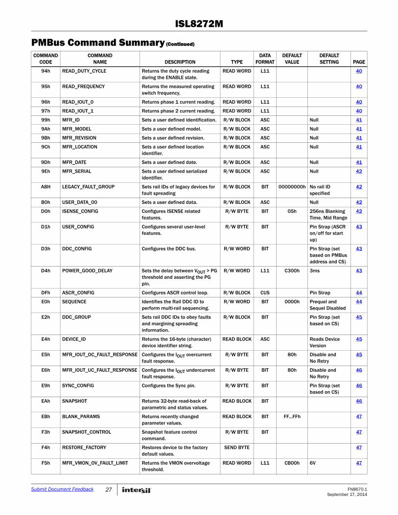
ISL8272M
94h READ_DUTY_CYCLE Returns the duty cycle reading during the ENABLE state.
READ WORD L11 40
95h READ_FREQUENCY Returns the measured operating switch frequency.
READ WORD L11 40
96h READ_IOUT_0 Returns phase 1 current reading. READ WORD L11 40
97h READ_IOUT_1 Returns phase 2 current reading. READ WORD L11 40
99h MFR_ID Sets a user defined identification. R/W BLOCK ASC Null 41
9Ah MFR_MODEL Sets a user defined model. R/W BLOCK ASC Null 41
9Bh MFR_REVISION Sets a user defined revision. R/W BLOCK ASC Null 41
9Ch MFR_LOCATION Sets a user defined location identifier.
R/W BLOCK ASC Null 41
9Dh MFR_DATE Sets a user defined date. R/W BLOCK ASC Null 41
9Eh MFR_SERIAL Sets a user defined serialized identifier.
R/W BLOCK ASC Null 42
A8H LEGACY_FAULT_GROUP Sets rail IDs of legacy devices for fault spreading
R/W BLOCK BIT 00000000h No rail ID specified
42
B0h USER_DATA_00 Sets a user defined data. R/W BLOCK ASC Null 42
D0h ISENSE_CONFIG Configures ISENSE related features.
R/W BYTE BIT 05h 256ns Blanking Time, Mid Range
42
D1h USER_CONFIG Configures several user-level features.
R/W BYTE BIT Pin Strap (ASCR on/off for start up)
43
D3h DDC_CONFIG Configures the DDC bus. R/W WORD BIT Pin Strap (set based on PMBus address and CS)
43
D4h POWER_GOOD_DELAY Sets the delay between VOUT > PG threshold and asserting the PG pin.
R/W WORD L11 C300h 3ms 43
DFh ASCR_CONFIG Configures ASCR control loop. R/W BLOCK CUS Pin Strap 44
E0h SEQUENCE Identifies the Rail DDC ID to perform multi-rail sequencing.
R/W WORD BIT 0000h Prequel and Sequel Disabled
44
E2h DDC_GROUP Sets rail DDC IDs to obey faults and margining spreading information.
R/W BLOCK BIT Pin Strap (set based on CS)
45
E4h DEVICE_ID Returns the 16-byte (character) device identifier string.
READ BLOCK ASC Reads Device Version
45
E5h MFR_IOUT_OC_FAULT_RESPONSE Configures the IOUT overcurrent fault response.
R/W BYTE BIT 80h Disable andNo Retry
45
E6h MFR_IOUT_UC_FAULT_RESPONSE Configures the IOUT undercurrent fault response.
R/W BYTE BIT 80h Disable andNo Retry
46
E9h SYNC_CONFIG Configures the Sync pin. R/W BYTE BIT Pin Strap (set based on CS)
46
EAh SNAPSHOT Returns 32-byte read-back of parametric and status values.
READ BLOCK BIT 46
EBh BLANK_PARAMS Returns recently changed parameter values.
READ BLOCK BIT FF...FFh 47
F3h SNAPSHOT_CONTROL Snapshot feature control command.
R/W BYTE BIT 47
F4h RESTORE_FACTORY Restores device to the factory default values.
SEND BYTE 47
F5h MFR_VMON_OV_FAULT_LIMIT Returns the VMON overvoltage threshold.
READ WORD L11 CB00h 6V 47
PMBus Command Summary (Continued)
COMMAND CODE
COMMAND NAME DESCRIPTION TYPE
DATAFORMAT
DEFAULT VALUE
DEFAULT SETTING PAGE
27 FN8670.1September 17, 2014
Submit Document Feedback
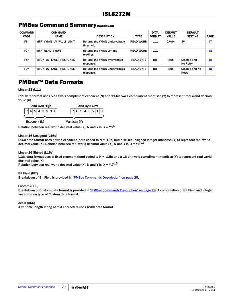
ISL8272M
PMBus™ Data FormatsLinear-11 (L11)
L11 data format uses 5-bit two’s compliment exponent (N) and 11-bit two’s compliment mantissa (Y) to represent real world decimal value (X).
Relation between real world decimal value (X), N and Y is: X = Y·2N
Linear-16 Unsigned (L16u) L16u data format uses a fixed exponent (hard-coded to N = -13h) and a 16-bit unsigned integer mantissa (Y) to represent real world decimal value (X). Relation between real world decimal value (X), N and Y is: X = Y·2-13
Linear-16 Signed (L16s) L16s data format uses a fixed exponent (hard-coded to N = -13h) and a 16-bit two’s compliment mantissa (Y) to represent real world decimal value (X). Relation between real world decimal value (X), N and Y is: X = Y·2-13
Bit Field (BIT)Breakdown of Bit Field is provided in “PMBus Commands Description” on page 29.
Custom (CUS)Breakdown of Custom data format is provided in “PMBus Commands Description” on page 29. A combination of Bit Field and integer are common type of Custom data format.
ASCII (ASC)A variable length string of text characters uses ASCII data format.
F6h MFR_VMON_UV_FAULT_LIMIT Returns the VMON undervoltage threshold.
READ WORD L11 CA00h 4V 47
F7h MFR_READ_VMON Returns the VMON voltage reading.
READ WORD L11 48
F8h VMON_OV_FAULT_RESPONSE Returns the VMON overvoltage response.
READ BYTE BIT 80h Disable andNo Retry
48
F9h VMON_UV_FAULT_RESPONSE Returns the VMON undervoltage response.
READ BYTE BIT 80h Disable and No Retry
48
PMBus Command Summary (Continued)
COMMAND CODE
COMMAND NAME DESCRIPTION TYPE
DATAFORMAT
DEFAULT VALUE
DEFAULT SETTING PAGE
Data Byte High Data Byte Low
Exponent (N) Mantissa (Y)
7 6 5 4 3 2 1 0 7 6 5 4 3 2 1 0
28 FN8670.1September 17, 2014
Submit Document Feedback
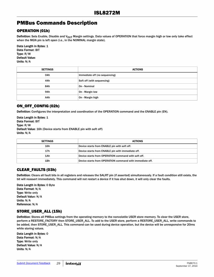
ISL8272M
PMBus Commands DescriptionOPERATION (01h)Definition: Sets Enable, Disable and VOUT Margin settings. Data values of OPERATION that force margin high or low only take effect when the MGN pin is left open (i.e., in the NOMINAL margin state).
Data Length in Bytes: 1Data Format: BITType: R/WDefault Value:Units: N/A
ON_OFF_CONFIG (02h)Definition: Configures the interpretation and coordination of the OPERATION command and the ENABLE pin (EN).
Data Length in Bytes: 1Data Format: BITType: R/WDefault Value: 16h (Device starts from ENABLE pin with soft off)Units: N/A
CLEAR_FAULTS (03h)Definition: Clears all fault bits in all registers and releases the SALRT pin (if asserted) simultaneously. If a fault condition still exists, the bit will reassert immediately. This command will not restart a device if it has shut down, it will only clear the faults.
Data Length in Bytes: 0 ByteData Format: N/AType: Write only Default Value: N/AUnits: N/A Reference: N/A
STORE_USER_ALL (15h)Definition: Stores all PMBus settings from the operating memory to the nonvolatile USER store memory. To clear the USER store, perform a RESTORE_FACTORY then STORE_USER_ALL. To add to the USER store, perform a RESTORE_USER_ALL, write commands to be added, then STORE_USER_ALL. This command can be used during device operation, but the device will be unresponsive for 20ms while storing values.
Data Length in Bytes: 0Data Format: N/AType: Write onlyDefault Value: N/AUnits: N/A
SETTINGS ACTIONS
04h Immediate off (no sequencing)
44h Soft off (with sequencing)
84h On - Nominal
94h On - Margin low
A4h On - Margin high
SETTINGS ACTIONS
16h Device starts from ENABLE pin with soft off.
17h Device starts from ENABLE pin with immediate off.
1Ah Device starts from OPERATION command with soft off.
1Bh Device starts from OPERATION command with immediate off.
29 FN8670.1September 17, 2014
Submit Document Feedback
ISL8272M
RESTORE_USER_ALL (16h)Definition: Restores all PMBus settings from the USER store memory to the operating memory. Command performed at power-up. Security level is changed to Level 1 following this command. This command can be used during device operation, but the device will be unresponsive for 20ms while storing values.
Data Length in Bytes: 0Data Format: N/AType: Write onlyDefault Value: N/AUnits: N/A
VOUT_MODE (20h)Definition: Reports the VOUT mode and provides the exponent used in calculating several VOUT settings. Fixed with linear mode with default exponent (N) = -13 Data Length in Bytes: 1Data Format: BITType: Read-onlyDefault Value: 13h (Linear Mode, N = -13)Units: N/A
VOUT_COMMAND (21h)Definition: This command sets or reports the target output voltage. This command cannot set a value higher than either VOUT_MAX or 110% of the pin strap VOUT setting.Data Length in Bytes: 2Data Format: L16uType: R/WDefault Value: Pin strap settingUnits: VoltsRange: 0V to VOUT_MAX
VOUT_CAL_OFFSET (23h)Definition: The VOUT_CAL_OFFSET command is used to apply a fixed offset voltage to the output voltage command value. This command is typically used by the user to calibrate a device in the application circuit. Data Length in Bytes: 2Data Format: L16sType: R/WDefault Value: 0000hUnits: Volts
VOUT_MAX (24h)Definition: The VOUT_ MAX command sets an upper limit on the output voltage the unit can command regardless of any other commands or combinations. The intent of this command is to provide a safeguard against a user accidentally setting the output voltage to a possibly destructive level rather than to be the primary output overprotection. Default value can be changed via PMBus. Data Length in Bytes: 2Data Format: L16uType: R/WDefault Value: 1.10xVOUT_COMMAND pin strap settingUnits: VoltsRange: 0V to 5.5V
VOUT_MARGIN_HIGH (25h)Definition: Sets the value of the VOUT during a margin high. This VOUT_MARGIN_HIGH command loads the unit with the voltage to which the output is to be changed when the OPERATION command or MGN pin is set to “Margin High”. Data Length in Bytes: 2Data Format: L16uType: R/WDefault value: 1.05 x VOUT_COMMAND pin strap settingUnits: VRange: 0V to VOUT_MAX
30 FN8670.1September 17, 2014
Submit Document Feedback
ISL8272M
VOUT_MARGIN_LOW (26h)Definition: Sets the value of the VOUT during a margin low. This VOUT_MARGIN_LOW command loads the unit with the voltage to which the output is to be changed when the OPERATION command or MGN pin is set to “Margin Low”. Data Length in Bytes: 2Data Format: L16uType: R/WDefault value: 0.95 x VOUT_COMMAND pin strap setting Units: VRange: 0V to VOUT_MAX
VOUT_TRANSITION_RATE (27h)Definition: This command sets the rate at which the output should change voltage when the device receives the VOUT_COMMAND or an OPERATION command (Margin High, Margin Low) that causes the output voltage to change. The maximum possible positive value of the two data bytes indicates that the device should make the transition as quickly as possible.Data Length in Bytes: 2Data Format: L11Type: R/WDefault value: BA00h (1.0 V/ms)Units: V/msRange: 0.1 to 4V/ms
VOUT_DROOP (28h)Definition: The VOUT_DROOP sets the effective load line (V/I slope) for the rail in which the device is used. It is the rate, in mV/A at which the output voltage decreases (or increases) with increasing (or decreasing) output current for use with Adaptive Voltage Positioning schemes or multi-module current sharing. In current sharing configuration, VOUT_DROOP set in each module stands for the droop seen by the load.Data Length in Bytes: 2Data Format: L11Type: R/WDefault value: Pin strap settingUnits: mV/ARange: 0 to 40mV/A
FREQUENCY_SWITCH (33h)Definition: Sets the switching frequency of the device. Initial default value is defined by a pin strap and this value can be overridden by writing this command via PMBus. If an external SYNC is utilized, this value should be set as close as possible to the external clock value. The output must be disabled when writing this command.Data Length in Bytes: 2Data Format: L11Type: R/WDefault Value: Pin strap settingUnits: kHzRange: 300kHz to 1066kHz
INTERLEAVE (37h)Definition: Configures the phase offset of a device that is sharing a common SYNC clock with other devices. The phase offset of each device can be set to any value between 0° and 360° in 22.5° increments. The internal two phases of the module always maintain a phase difference of 180°.Data Length in Bytes: 2Data Format: BITType: R/WDefault Value: 0000hUnits: N/A
BITS PURPOSE VALUE DESCRIPTION
15:4 Reserved 0 Reserved
3:0 Position in Group 0 to 15 Sets position of the device's rail within the group.
31 FN8670.1September 17, 2014
Submit Document Feedback
ISL8272M
IOUT_CAL_GAIN (38h)Definition: Sets the effective impedance across the current sense circuit for use in calculating output current at +25°C.Data Length in Bytes: 2Data Format: L11Type: R/WDefault Value: B370h (0.86mΩ)Units: mΩ
IOUT_CAL_OFFSET (39h)Definition: Used to null out any offsets in the output current sensing circuit, and to compensate for delayed measurements of current ramp due to Isense blanking time.Data Length in Bytes: 2Data Format: L11Type: R/WDefault Value: 0000h (0A)Units: A
VOUT_OV_FAULT_LIMIT (40h)Definition: Sets the VOUT overvoltage fault threshold.Data Length in Bytes: 2Data Format: L16uType: R/WDefault Value: 1.15xVOUT_COMMAND pin strap settingUnits: VRange: 0V to VOUT_MAX
VOUT_OV_FAULT_RESPONSE (41h)Definition: Configures the VOUT overvoltage fault response. Note that the device cannot be set to ignore this fault mode.Data Length in Bytes: 1Data Format: BITType: R/WDefault Value: 80h (Disable and no retry)Units: N/A
VOUT_OV_WARN_LIMIT (42h)Definition: Sets the VOUT overvoltage warning threshold. Power-good signal is pulled low when output voltage goes higher than this threshold. Data Length in Bytes: 2Data Format: L16uType: R/WDefault Value: 1.10xVOUT_COMMAND pin strap settingUnits: VRange: 0V to VOUT_MAX
VOUT_UV_WARN_LIMIT (43h)Definition: Sets the VOUT undervoltage warning threshold. Power-good signal is pulled low when output voltage goes lower than this threshold.Data Length in Bytes: 2Data Format: L16uType: R/WDefault Value: 0.90xVOUT_COMMAND pin strap settingUnits: VRange: 0V to VOUT_MAX
SETTINGS ACTIONS
80h Disable with no retry.
BFh Disable and continuous retry with 70ms delay.
32 FN8670.1September 17, 2014
Submit Document Feedback
ISL8272M
VOUT_UV_FAULT_LIMIT (44h)Definition: Sets the VOUT undervoltage fault threshold. This fault is masked during ramp or when disabled.Data Length in Bytes: 2Data Format: L16uType: R/WDefault Value: 0.85xVOUT_COMMAND pin strap settingUnits: VRange: 0V to VOUT_MAX
VOUT_UV_FAULT_RESPONSE (45h)Definition: Configures the VOUT undervoltage fault response. Data Length in Bytes: 1Data Format: BITType: R/WDefault Value: 80h (Disable, no retry)Units: N/A
IOUT_OC_FAULT_LIMIT (46h)Definition: Sets the IOUT average overcurrent fault threshold. Device will automatically calculate peak inductor overcurrent fault limit for each phase based on the equation: IOUT(PEAK OC LIMIT)=(0.5*IOUT_OC_FAULT_LIMIT+0.5*IRIPPLE(P-P))*120%. A hard bound of 42A is applied to the peak overcurrent fault limit per phase.Data Length in Bytes: 2
Data Format: L11Type: R/WDefault Value: E3C0h (60A)Units: ARange: -100 to 100A
IOUT_UC_FAULT_LIMIT (4Bh)Definition: Sets the IOUT average undercurrent fault threshold. Device will automatically calculate valley inductor undercurrent fault limit for each phase based on the equation: IOUT(VALLEY UC LIMIT)=(0.5*IOUT_UC_FAULT_LIMIT-0.5*IRIPPLE(P-P))*120%. A hard bound of -42A is applied to the valley undercurrent fault limit per phase.Data Length in Bytes: 2Data Format: L11Type: R/WDefault Value: -1xIOUT_OC_FAULT_LIMITUnits: ARange: -100 to 100A
OT_FAULT_LIMIT (4Fh)Definition: The OT_FAULT_LIMIT command sets the temperature at which the device should indicate an over-temperature fault. Note that the temperature must drop below OT_WARN_LIMIT to clear this fault.Data Length in Bytes: 2Data Format: L11Type: R/WDefault Value: EBE8h (+125˚C)Units: CelsiusRange: 0°C to +175°C
SETTINGS ACTIONS
80h Disable with no retry.
BFh Disable and continuous retry with 70ms delay.
33 FN8670.1September 17, 2014
Submit Document Feedback
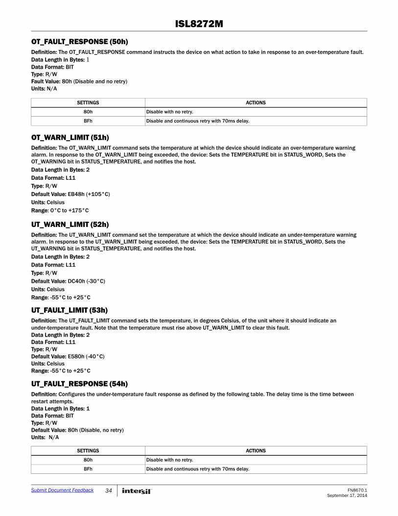
ISL8272M
OT_FAULT_RESPONSE (50h) Definition: The OT_FAULT_RESPONSE command instructs the device on what action to take in response to an over-temperature fault. Data Length in Bytes: 1Data Format: BITType: R/WFault Value: 80h (Disable and no retry)Units: N/A
OT_WARN_LIMIT (51h)Definition: The OT_WARN_LIMIT command sets the temperature at which the device should indicate an over-temperature warning alarm. In response to the OT_WARN_LIMIT being exceeded, the device: Sets the TEMPERATURE bit in STATUS_WORD, Sets the OT_WARNING bit in STATUS_TEMPERATURE, and notifies the host.Data Length in Bytes: 2Data Format: L11Type: R/WDefault Value: EB48h (+105°C)Units: CelsiusRange: 0°C to +175°C
UT_WARN_LIMIT (52h)Definition: The UT_WARN_LIMIT command set the temperature at which the device should indicate an under-temperature warning alarm. In response to the UT_WARN_LIMIT being exceeded, the device: Sets the TEMPERATURE bit in STATUS_WORD, Sets the UT_WARNING bit in STATUS_TEMPERATURE, and notifies the host.Data Length in Bytes: 2Data Format: L11Type: R/WDefault Value: DC40h (-30°C)Units: CelsiusRange: -55°C to +25°C
UT_FAULT_LIMIT (53h)Definition: The UT_FAULT_LIMIT command sets the temperature, in degrees Celsius, of the unit where it should indicate an under-temperature fault. Note that the temperature must rise above UT_WARN_LIMIT to clear this fault.Data Length in Bytes: 2Data Format: L11Type: R/WDefault Value: E580h (-40°C)Units: CelsiusRange: -55°C to +25°C
UT_FAULT_RESPONSE (54h)Definition: Configures the under-temperature fault response as defined by the following table. The delay time is the time between restart attempts.Data Length in Bytes: 1Data Format: BITType: R/WDefault Value: 80h (Disable, no retry)Units: N/A
SETTINGS ACTIONS
80h Disable with no retry.
BFh Disable and continuous retry with 70ms delay.
SETTINGS ACTIONS
80h Disable with no retry.
BFh Disable and continuous retry with 70ms delay.
34 FN8670.1September 17, 2014
Submit Document Feedback
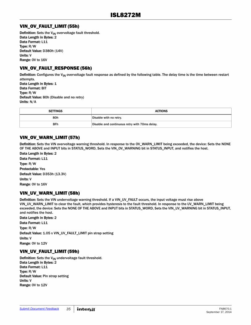
ISL8272M
VIN_OV_FAULT_LIMIT (55h)Definition: Sets the VIN overvoltage fault threshold.Data Length in Bytes: 2Data Format: L11Type: R/WDefault Value: D380h (14V)Units: VRange: 0V to 16V
VIN_OV_FAULT_RESPONSE (56h)Definition: Configures the VIN overvoltage fault response as defined by the following table. The delay time is the time between restart attempts.Data Length in Bytes: 1Data Format: BITType: R/WDefault Value: 80h (Disable and no retry)Units: N/A
VIN_OV_WARN_LIMIT (57h)Definition: Sets the VIN overvoltage warning threshold. In response to the OV_WARN_LIMIT being exceeded, the device: Sets the NONE OF THE ABOVE and INPUT bits in STATUS_WORD, Sets the VIN_OV_WARNING bit in STATUS_INPUT, and notifies the host.Data Length in Bytes: 2Data Format: L11Type: R/WProtectable: YesDefault Value: D353h (13.3V)Units: VRange: 0V to 16V
VIN_UV_WARN_LIMIT (58h)Definition: Sets the VIN undervoltage warning threshold. If a VIN_UV_FAULT occurs, the input voltage must rise above VIN_UV_WARN_LIMIT to clear the fault, which provides hysteresis to the fault threshold. In response to the UV_WARN_LIMIT being exceeded, the device: Sets the NONE OF THE ABOVE and INPUT bits in STATUS_WORD, Sets the VIN_UV_WARNING bit in STATUS_INPUT, and notifies the host.Data Length in Bytes: 2Data Format: L11Type: R/WDefault Value: 1.05 x VIN_UV_FAULT_LIMIT pin strap settingUnits: VRange: 0V to 12V
VIN_UV_FAULT_LIMIT (59h)Definition: Sets the VIN undervoltage fault threshold. Data Length in Bytes: 2Data Format: L11Type: R/WDefault Value: Pin strap settingUnits: VRange: 0V to 12V
SETTINGS ACTIONS
80h Disable with no retry.
BFh Disable and continuous retry with 70ms delay.
35 FN8670.1September 17, 2014
Submit Document Feedback
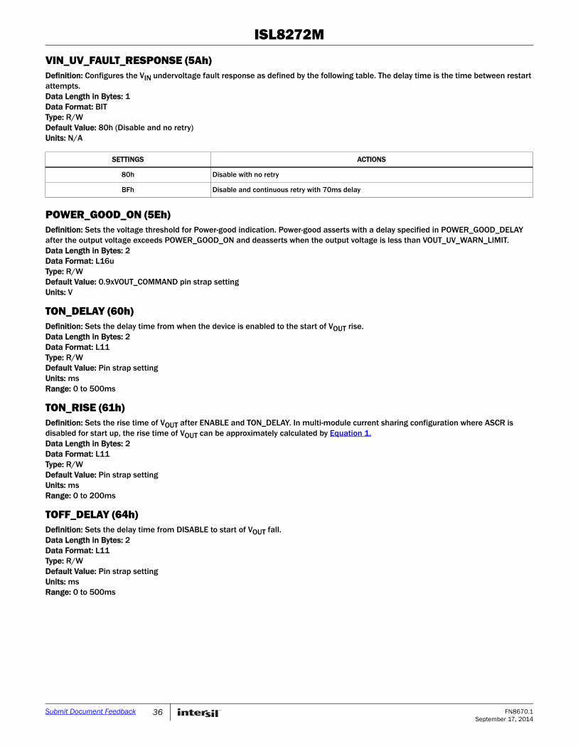
ISL8272M
VIN_UV_FAULT_RESPONSE (5Ah)Definition: Configures the VIN undervoltage fault response as defined by the following table. The delay time is the time between restart attempts.Data Length in Bytes: 1Data Format: BITType: R/WDefault Value: 80h (Disable and no retry)Units: N/A
POWER_GOOD_ON (5Eh)Definition: Sets the voltage threshold for Power-good indication. Power-good asserts with a delay specified in POWER_GOOD_DELAY after the output voltage exceeds POWER_GOOD_ON and deasserts when the output voltage is less than VOUT_UV_WARN_LIMIT.Data Length in Bytes: 2Data Format: L16uType: R/WDefault Value: 0.9xVOUT_COMMAND pin strap settingUnits: V
TON_DELAY (60h)Definition: Sets the delay time from when the device is enabled to the start of VOUT rise. Data Length in Bytes: 2Data Format: L11Type: R/WDefault Value: Pin strap settingUnits: msRange: 0 to 500ms
TON_RISE (61h)Definition: Sets the rise time of VOUT after ENABLE and TON_DELAY. In multi-module current sharing configuration where ASCR is disabled for start up, the rise time of VOUT can be approximately calculated by Equation 1.Data Length in Bytes: 2Data Format: L11Type: R/WDefault Value: Pin strap settingUnits: msRange: 0 to 200ms
TOFF_DELAY (64h)Definition: Sets the delay time from DISABLE to start of VOUT fall. Data Length in Bytes: 2Data Format: L11Type: R/WDefault Value: Pin strap settingUnits: msRange: 0 to 500ms
SETTINGS ACTIONS
80h Disable with no retry
BFh Disable and continuous retry with 70ms delay
36 FN8670.1September 17, 2014
Submit Document Feedback
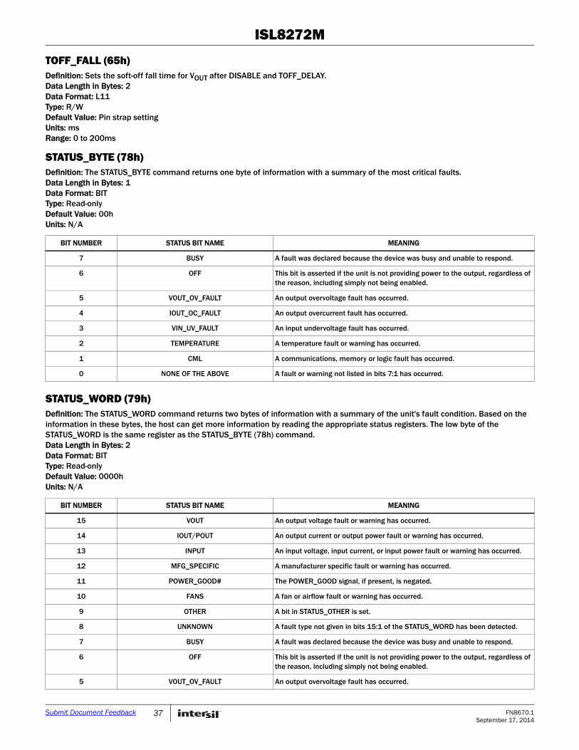
ISL8272M
TOFF_FALL (65h)Definition: Sets the soft-off fall time for VOUT after DISABLE and TOFF_DELAY. Data Length in Bytes: 2Data Format: L11Type: R/WDefault Value: Pin strap settingUnits: msRange: 0 to 200ms
STATUS_BYTE (78h)Definition: The STATUS_BYTE command returns one byte of information with a summary of the most critical faults.Data Length in Bytes: 1Data Format: BITType: Read-onlyDefault Value: 00h Units: N/A
STATUS_WORD (79h)Definition: The STATUS_WORD command returns two bytes of information with a summary of the unit's fault condition. Based on the information in these bytes, the host can get more information by reading the appropriate status registers. The low byte of the STATUS_WORD is the same register as the STATUS_BYTE (78h) command.Data Length in Bytes: 2Data Format: BITType: Read-onlyDefault Value: 0000hUnits: N/A
BIT NUMBER STATUS BIT NAME MEANING
7 BUSY A fault was declared because the device was busy and unable to respond.
6 OFF This bit is asserted if the unit is not providing power to the output, regardless of the reason, including simply not being enabled.
5 VOUT_OV_FAULT An output overvoltage fault has occurred.
4 IOUT_OC_FAULT An output overcurrent fault has occurred.
3 VIN_UV_FAULT An input undervoltage fault has occurred.
2 TEMPERATURE A temperature fault or warning has occurred.
1 CML A communications, memory or logic fault has occurred.
0 NONE OF THE ABOVE A fault or warning not listed in bits 7:1 has occurred.
BIT NUMBER STATUS BIT NAME MEANING
15 VOUT An output voltage fault or warning has occurred.
14 IOUT/POUT An output current or output power fault or warning has occurred.
13 INPUT An input voltage, input current, or input power fault or warning has occurred.
12 MFG_SPECIFIC A manufacturer specific fault or warning has occurred.
11 POWER_GOOD# The POWER_GOOD signal, if present, is negated.
10 FANS A fan or airflow fault or warning has occurred.
9 OTHER A bit in STATUS_OTHER is set.
8 UNKNOWN A fault type not given in bits 15:1 of the STATUS_WORD has been detected.
7 BUSY A fault was declared because the device was busy and unable to respond.
6 OFF This bit is asserted if the unit is not providing power to the output, regardless of the reason, including simply not being enabled.
5 VOUT_OV_FAULT An output overvoltage fault has occurred.
37 FN8670.1September 17, 2014
Submit Document Feedback
ISL8272M
STATUS_VOUT (7Ah)Definition: The STATUS_VOUT command returns one data byte with the status of the output voltage.Data Length in Bytes: 1Data Format: BITType: Read-onlyDefault Value: 00hUnits: N/A
STATUS_IOUT (7Bh)Definition: The STATUS_IOUT command returns one data byte with the status of the output current.Data Length in Bytes: 1Data Format: BITType: Read-onlyDefault Value: 00hUnits: N/A
STATUS_INPUT (7Ch)Definition: The STATUS_INPUT command returns input voltage and input current status information.Data Length in Bytes: 1Data Format: BITType: Read-onlyDefault Value: 00hUnits: N/A
4 IOUT_OC_FAULT An output overcurrent fault has occurred.
3 VIN_UV_FAULT An input undervoltage fault has occurred.
2 TEMPERATURE A temperature fault or warning has occurred.
1 CML A communications, memory or logic fault has occurred.
0 NONE OF THE ABOVE A fault or warning not listed in bits 7:1 has occurred.
BIT NUMBER STATUS BIT NAME MEANING
7 VOUT_OV_FAULT Indicates an output overvoltage fault.
6 VOUT_OV_WARNING Indicates an output overvoltage warning.
5 VOUT_UV_WARNING Indicates an output undervoltage warning.
4 VOUT_UV_FAULT Indicates an output undervoltage fault.
3:0 N/A These bits are not used.
BIT NUMBER STATUS BIT NAME MEANING
7 IOUT_OC_FAULT An output overcurrent fault has occurred.
6 IOUT_OC_LV_FAULT An output overcurrent and low voltage fault has occurred.
5 IOUT_OC_WARNING An output overcurrent warning has occurred.
4 IOUT_UC_FAULT An output undercurrent fault has occurred.
3:0 N/A These bits are not used.
BIT NUMBER STATUS BIT NAME MEANING
7 VIN_OV_FAULT An input overvoltage fault has occurred.
6 VIN_OV_WARNING An input overvoltage warning has occurred.
5 VIN_UV_WARNING An input undervoltage warning has occurred.
4 VIN_UV_FAULT An input undervoltage fault has occurred.
3:0 N/A These bits are not used.
BIT NUMBER STATUS BIT NAME MEANING
38 FN8670.1September 17, 2014
Submit Document Feedback
ISL8272M
STATUS_TEMP (7Dh)Definition: The STATUS_TEMP command returns one byte of information with a summary of any temperature related faults or warnings.Data Length in Bytes: 1Data Format: BITType: Read-onlyDefault Value: 00hUnits: N/A
STATUS_CML (7Eh)Definition: The STATUS_CML command returns one byte of information with a summary of any Communications, Logic and/or Memory errors.Data Length in Bytes: 1Data Format: BITType: Read-onlyDefault Value: 00hUnits: N/A
STATUS_MFR_SPECIFIC (80h)Definition: The STATUS_MFR_SPECIFIC command returns one byte of information providing the status of the device's voltage monitoring and clock synchronization faults. VMON OV/UV warnings are set at ±10% of the VMON_FAULT commands.Data Length in Bytes: 1Data Format: BITType: Read onlyDefault value: 00hUnits: N/A
BIT NUMBER STATUS BIT NAME MEANING
7 OT_FAULT An over-temperature fault has occurred.
6 OT_WARNING An over-temperature warning has occurred.
5 UT_WARNING An under-temperature warning has occurred.
4 UT_FAULT An under-temperature fault has occurred.
3:0 N/A These bits are not used.
BIT NUMBER MEANING
7 Invalid or unsupported PMBus command was received.
6 The PMBus command was sent with invalid or unsupported data.
5 packet error was detected in the PMBus command.
4:2 Not Used
1 A PMBus command tried to write to a read-only or protected command, or a communication fault other than the ones listed in this table has occurred.
0 Not Used
BIT NUMBER FIELD NAME MEANING
7:6 Reserved
5 VMON UV Warning The voltage on the VMON pin has dropped 10% below the level set by VMON_UV_FAULT_LIMIT.
4 VMON OV Warning The voltage on the VMON pin has risen 10% above the level set by VMON_OV_FAULT_LIMIT.
3 External Switching Period Fault Loss of external clock synchronization has occurred.
2 Reserved
1 VMON UV Fault The voltage on the VMON pin has dropped below the level set by VMON_UV_FAULT_LIMIT.
0 VMON OV Fault The voltage on the VMON pin has risen above the level set by VMON_OV_FAULT_LIMIT.
39 FN8670.1September 17, 2014
Submit Document Feedback
ISL8272M
READ_VIN (88h)Definition: Returns the input voltage reading. Data Length in Bytes: 2Data Format: L11Type: Read-onlyUnits: V
READ_VOUT (8Bh)Definition: Returns the output voltage reading.Data Length in Bytes: 2Data Format: L16uType: Read-onlyUnits: V
READ_IOUT (8Ch)Definition: Returns the output current reading. Data Length in Bytes: 2Data Format: L11Type: Read-onlyDefault Value: N/AUnits: A
READ_INTERNAL_TEMP (8Dh)Definition: Returns the controller junction temperature reading from internal temperature sensor. Data Length in Bytes: 2Data Format: L11Type: Read-onlyUnits: °C
READ_DUTY_CYCLE (94h)Definition: Reports the actual duty cycle of the converter during the enable state. Data Length in Bytes: 2Data Format: L11Type: Read onlyUnits: %
READ_FREQUENCY (95h)Definition: Reports the actual switching frequency of the converter during the enable state. Data Length in Bytes: 2Data Format: L11Type: Read onlyUnits: kHz
READ_IOUT_0 (96h)Definition: Returns the Phase 1 current reading. Data Length in Bytes: 2Data Format: L11Type: Read-onlyDefault Value: N/AUnits: A
READ_IOUT_1 (97h)Definition: Returns the Phase 2 current reading. Data Length in Bytes: 2Data Format: L11Type: Read-onlyDefault Value: N/AUnits: A
40 FN8670.1September 17, 2014
Submit Document Feedback
ISL8272M
MFR_ID (99h)Definition: MFR_ID sets user defined identification. The sum total of characters in MFR_ID, MFR_MODEL, MFR_REVISION, MFR_LOCATION, MFR_DATE, MFR_SERIAL and USER_DATA_00 plus one byte per command cannot exceed 128 characters. This limitation includes multiple writes of this command before a STORE command. To clear multiple writes, perform a RESTORE, write this command then perform a STORE/RESTORE.Data Length in Bytes: user definedData Format: ASCIIType: Block R/WDefault Value: nullUnits: N/A
MFR_MODEL (9Ah)Definition: MFR_MODEL sets a user defined model. The sum total of characters in MFR_ID, MFR_MODEL, MFR_REVISION, MFR_LOCATION, MFR_DATE, MFR_SERIAL and USER_DATA_00 plus one byte per command cannot exceed 128 characters. This limitation includes multiple writes of this command before a STORE command. To clear multiple writes, perform a RESTORE, write this command then perform a STORE/RESTORE.Data Length in Bytes: user defined Data Format: ASCType: Block R/WDefault Value: nullUnits: N/A
MFR_REVISION (9Bh)Definition: MFR_REVISION sets a user defined revision. The sum total of characters in MFR_ID, MFR_MODEL, MFR_REVISION, MFR_LOCATION, MFR_DATE, MFR_SERIAL and USER_DATA_00 plus one byte per command cannot exceed 128 characters. This limitation includes multiple writes of this command before a STORE command. To clear multiple writes, perform a RESTORE, write this command then perform a STORE/RESTORE.Data Length in Bytes: user defined Data Format: ASCType: Block R/WDefault Value: nullUnits: N/A
MFR_LOCATION (9Ch)Definition: MFR_LOCATION sets a user defined location identifier. The sum total of characters in MFR_ID, MFR_MODEL, MFR_REVISION, MFR_LOCATION, MFR_DATE, MFR_SERIAL and USER_DATA_00 plus one byte per command cannot exceed 128 characters. This limitation includes multiple writes of this command before a STORE command. To clear multiple writes, perform a RESTORE, write this command then perform a STORE/RESTORE.Data Length in Bytes: user definedData Format: ASCType: Block R/WDefault Value: nullUnits: N/A
MFR_DATE (9Dh)Definition: MFR_DATE sets a user defined date. The sum total of characters in MFR_ID, MFR_MODEL, MFR_REVISION, MFR_LOCATION, MFR_DATE, MFR_SERIAL and USER_DATA_00 plus one byte per command cannot exceed 128 characters. This limitation includes multiple writes of this command before a STORE command. To clear multiple writes, perform a RESTORE, write this command then perform a STORE/RESTORE.Data Length in Bytes: user definedData Format: ASCType: Block R/WDefault Value: nullUnits: N/AReference: N/A
41 FN8670.1September 17, 2014
Submit Document Feedback
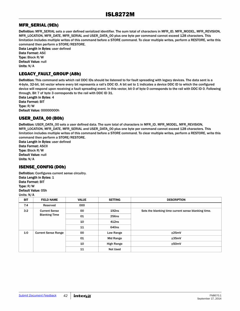
ISL8272M
MFR_SERIAL (9Eh)Definition: MFR_SERIAL sets a user defined serialized identifier. The sum total of characters in MFR_ID, MFR_MODEL, MFR_REVISION, MFR_LOCATION, MFR_DATE, MFR_SERIAL and USER_DATA_00 plus one byte per command cannot exceed 128 characters. This limitation includes multiple writes of this command before a STORE command. To clear multiple writes, perform a RESTORE, write this command then perform a STORE/RESTORE.Data Length in Bytes: user definedData Format: ASCType: Block R/WDefault Value: nullUnits: N/A
LEGACY_FAULT_GROUP (A8h)Definition: This command sets which rail DDC IDs should be listened to for fault spreading with legacy devices. The data sent is a 4-byte, 32-bit, bit vector where every bit represents a rail’s DDC ID. A bit set to 1 indicates a device DDC ID to which the configured device will respond upon receiving a fault spreading event. In this vector, bit 0 of byte 0 corresponds to the rail with DDC ID 0. Following through, Bit 7 of byte 3 corresponds to the rail with DDC ID 31.Data Length in Bytes: 4Data Format: BITType: R/WDefault Value: 00000000h
USER_DATA_00 (B0h)Definition: USER_DATA_00 sets a user defined data. The sum total of characters in MFR_ID, MFR_MODEL, MFR_REVISION, MFR_LOCATION, MFR_DATE, MFR_SERIAL and USER_DATA_00 plus one byte per command cannot exceed 128 characters. This limitation includes multiple writes of this command before a STORE command. To clear multiple writes, perform a RESTORE, write this command then perform a STORE/RESTORE.Data Length in Bytes: user definedData Format: ASCIIType: Block R/WDefault Value: nullUnits: N/A
ISENSE_CONFIG (D0h)Definition: Configures current sense circuitry.Data Length in Bytes: 1Data Format: BITType: R/WDefault Value: 05hUnits: N/A
BIT FIELD NAME VALUE SETTING DESCRIPTION
7:4 Reserved 000
3:2 Current Sense Blanking Time
00 192ns Sets the blanking time current sense blanking time.
01 256ns
10 412ns
11 640ns
1:0 Current Sense Range 00 Low Range ±25mV
01 Mid Range ±35mV
10 High Range ±50mV
11 Not Used
42 FN8670.1September 17, 2014
Submit Document Feedback
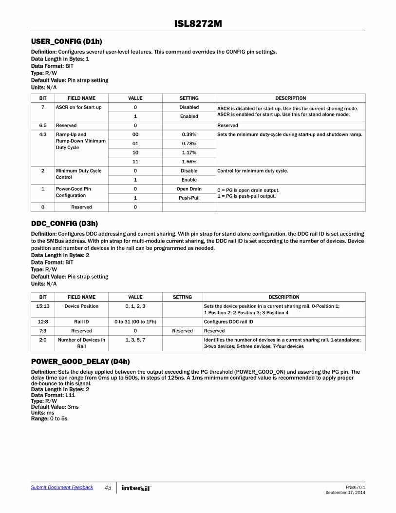
ISL8272M
USER_CONFIG (D1h)Definition: Configures several user-level features. This command overrides the CONFIG pin settings.Data Length in Bytes: 1Data Format: BITType: R/WDefault Value: Pin strap settingUnits: N/A
DDC_CONFIG (D3h)Definition: Configures DDC addressing and current sharing. With pin strap for stand alone configuration, the DDC rail ID is set according to the SMBus address. With pin strap for multi-module current sharing, the DDC rail ID is set according to the number of devices. Device position and number of devices in the rail can be programmed as needed.Data Length in Bytes: 2Data Format: BITType: R/WDefault Value: Pin strap settingUnits: N/A
POWER_GOOD_DELAY (D4h)Definition: Sets the delay applied between the output exceeding the PG threshold (POWER_GOOD_ON) and asserting the PG pin. The delay time can range from 0ms up to 500s, in steps of 125ns. A 1ms minimum configured value is recommended to apply proper de-bounce to this signal. Data Length in Bytes: 2Data Format: L11Type: R/WDefault Value: 3msUnits: ms Range: 0 to 5s
BIT FIELD NAME VALUE SETTING DESCRIPTION
7 ASCR on for Start up 0 Disabled ASCR is disabled for start up. Use this for current sharing mode.ASCR is enabled for start up. Use this for stand alone mode.1 Enabled
6:5 Reserved 0 Reserved
4:3 Ramp-Up and Ramp-Down Minimum Duty Cycle
00 0.39% Sets the minimum duty-cycle during start-up and shutdown ramp.
01 0.78%
10 1.17%
11 1.56%
2 Minimum Duty Cycle Control
0 Disable Control for minimum duty cycle.
1 Enable
1 Power-Good Pin Configuration
0 Open Drain 0 = PG is open drain output.1 = PG is push-pull output.1 Push-Pull
0 Reserved 0
BIT FIELD NAME VALUE SETTING DESCRIPTION
15:13 Device Position 0, 1, 2, 3 Sets the device position in a current sharing rail. 0-Position 1; 1-Position 2; 2-Position 3; 3-Position 4
12:8 Rail ID 0 to 31 (00 to 1Fh) Configures DDC rail ID
7:3 Reserved 0 Reserved Reserved
2:0 Number of Devices in Rail
1, 3, 5, 7 Identifies the number of devices in a current sharing rail. 1-standalone; 3-two devices; 5-three devices; 7-four devices
43 FN8670.1September 17, 2014
Submit Document Feedback
ISL8272M
ASCR_CONFIG (DFh)Definition: Allows user configuration of ASCR settings. ASCR Gain is analogous to bandwidth, ASCR Residual is analogous to damping. To improve load transient response performance, increase ASCR Gain. To lower transient response overshoot, increase ASCR Residual. Increasing ASCR gain can result in increased PWM jitter and should be evaluated in the application circuit. Excessive ASCR gain can lead to excessive output voltage ripple. Increasing ASCR Residual to improve transient response damping can result in slower recovery times, but will not affect the peak output voltage deviation. Typical ASCR Gain settings range from 50 to 1000, and ASCR Residual settings range from 10 to 100.
Data Length in Bytes: 4Data Format: CUSType: R/WDefault Value: Pin strap setting
SEQUENCE (E0h)Definition: Identifies the Rail DDC ID of the prequel and sequel rails when performing multi-rail sequencing. The device will enable its output when its EN or OPERATION enable states, as defined by ON_OFF_CONFIG, is set and the prequel device has issued a Power-Good event on the DDC bus. The device will disable its output (using the programmed delay values) when the sequel device has issued a Power-Down event on the DDC bus.
The data field is a two-byte value. The most-significant byte contains the 5-bit Rail DDC ID of the prequel device. The least-significant byte contains the 5-bit Rail DDC ID of the sequel device. The most significant bit of each byte contains the enable of the prequel or sequel mode. This command overrides the corresponding sequence configuration set by the CONFIG pin settings.Data Length in Bytes: 2Data Format: BITType: R/WDefault Value: 0000h (Prequel and Sequel disabled)
BIT PURPOSE DATA Format VALUE DESCRIPTION
31:25 Unused 0000000h Unused
24 ASCR Enable BIT1 Enable
0 Disable
23:16 ASCR Residual Setting Integer ASCR residual
15:0 ASCR Gain Setting Integer ASCR gain
BIT FIELD NAME VALUE SETTING DESCRIPTION
15Prequel Enable 0 Disable Disable, no prequel preceding this rail.
1 Enable Enable, prequel to this rail is defined by bits 12:8.
14:13 Reserved 0 Reserved Reserved
12:8 Prequel Rail DDC ID 0-31 DDC ID Set to the DDC ID of the prequel rail.
7Sequel Enable 0 Disable Disable, no sequel following this rail.
1 Enable Enable, sequel to this rail is defined by bits 4:0.
6:5 Reserved 0 Reserved Reserved
4:0 Sequel Rail DDC ID 0-31 DDC ID Set to the DDC ID of the sequel rail.
44 FN8670.1September 17, 2014
Submit Document Feedback
ISL8272M
DDC_GROUP (E2h)Definition: This command configures fault spreading group ID and enable, broadcast OPERATION group ID and enable, and broadcast VOUT_COMMAND group ID and enable.Data Length in Bytes: 3Data Format: BITType: R/WDefault Value: Pin strap setting (Ignore BROADCAST VOUT_COMMAND, OPERATION and fault for stand alone operation. Enable BROADCAST VOUT_COMMAND, OPERATION and fault for current sharing)
DEVICE_ID (E4h)Definition: Returns the 16-byte (character) device identifier string.Data Length in Bytes: 16Data Format: ASCIIType: Block ReadDefault Value: Part number/Die revision/Firmware revision
MFR_IOUT_OC_FAULT_RESPONSE (E5h)Definition: Configures the IOUT overcurrent fault response as defined by the following table. The command format is the same as the PMBus standard fault responses except that it sets the overcurrent status bit in STATUS_IOUT.Data Length in Bytes: 1Data Format: BITType: R/WDefault Value: 80h (Disable, and no retry)Units: N/A
BITS PURPOSE VALUE DESCRIPTION
23:22 Reserved 0 Reserved
21BROADCAST_VOUT_COMMAND Response 1 Responds to BROADCAST_VOUT_COMMAND with same Group ID.
0 Ignores BROADCAST_VOUT_COMMAND.
20:16 BROADCAST_VOUT_COMMAND Group ID 0-31d Group ID sent as data for broadcast BROADCAST_VOUT_COMMAND events.
15:14 Reserved 0 Reserved
13 BROADCAST_OPERATION Response 1 Responds to BROADCAST_OPERATION with same Group ID.
0 Ignores BROADCAST_OPERATION.
12:8 BROADCAST_OPERATION Group ID 0-31d Group ID sent as data for broadcast BROADCAST_OPERATION events.
7:6 Reserved 0 Reserved
5
POWER_FAIL Response 1 Responds to POWER_FAIL events with same Group ID by shutting down immediately.
0 Responds to POWER_FAIL events with same Group ID with sequenced shutdown.
4:0 POWER_FAIL group ID 0-31d Group ID sent as data for broadcast POWER_FAIL events.
SETTINGS ACTIONS
80h Disable with no retry.
BFh Disable and continuous retry with 70ms delay.
45 FN8670.1September 17, 2014
Submit Document Feedback
ISL8272M
MFR_IOUT_UC_FAULT_RESPONSE (E6h)Definition: Configures the IOUT undercurrent fault response as defined by the following table. The command format is the same as the PMBus standard fault responses except that it sets the undercurrent status bit in STATUS_IOUT.Data Length in Bytes: 1Data Format: BITType: R/WDefault Value: 80h (Disable and no retry)Units: N/A
SYNC_CONFIG (E9h)Definition: This command is used to set options for SYNC output configurations. Data Length in Bytes: 1Data Format: BITType: R/WDefault Value: Pin strap setting
SNAPSHOT (EAh)Definition: The SNAPSHOT command is a 32-byte read-back of parametric and status values. It allows monitoring and status data to be stored to flash following a fault condition. In case of a fault, last updated values are stored to the flash memory. When SNAPSHOT STATUS bit is set stored, device will no longer automatically capture parametric and status values following fault till stored data are erased. Use SNAPSHOT_CONTROL command to erase store data and clear the status bit before next ramp up. Data erased is not allowed when module is enabled. Data Length in Bytes: 32Data Format: Bit fieldType: Block Read
SETTINGS ACTIONS
80h Disable with no retry.
BFh Disable and continuous retry with 70ms delay.
SETTINGS ACTIONS
00h Use Internal clock. Clock frequency is set by pin strap or PMBus command.
02h Use internal clock and output internal clock.
04h Use external clock.
BYTE NUMBER VALUE PMBUS COMMAND FORMAT
31:23 Reserved Reserved 00h
22Flash Memory Status ByteFF - Not Stored00 - Stored
N/A BIT
21 Manufacturer Specific Status Byte STATUS_MFR_SPECIFIC (80h) Byte
20 CML Status Byte STATUS_CML (7Eh) Byte
19 Temperature Status Byte STATUS_TEMPERATURE (7Dh) Byte
18 Input Status Byte STATUS_INPUT (7Ch) Byte
17 IOUT Status Byte STATUS_IOUT (7Bh) Byte
16 VOUT Status Byte STATUS_VOUT (7Ah) Byte
15:14 Switching Frequency READ_FREQUENCY (95h) L11
13:12 Reserved Reserved 00h
11:10 Internal Temperature READ_INTERNAL_TEMP (8Dh) L11
9:8 Duty Cycle READ_DUTY_CYCLE (94h) L11
7:6 Highest Measured Output Current N/A L11
46 FN8670.1September 17, 2014
Submit Document Feedback
ISL8272M
BLANK_PARAMS (EBh)Definition: Returns a 16-byte string indicating which parameter values were either retrieved by the last RESTORE operation or have been written since that time. Reading BLANK_PARAMS immediately after a restore operation allows the user to determine which parameters are stored in that store. A one indicates the parameter is not present in the store and has not been written since the RESTORE operation. Data Length in Bytes: 16Data Format: BITType: Block ReadDefault Value: FF…FFh
SNAPSHOT_CONTROL (F3h)Definition: Writing a 01h will cause the device to copy the current SNAPSHOT values from NVRAM to the 32-byte SNAPSHOT command parameter. Writing a 02h will cause the device to write the current SNAPSHOT values to NVRAM, 03h will erase all SNAPSHOT values from NVRAM. Write (02h) and Erase (03h) may only be used when the device is disabled. All other values will be ignored.Data Length in Bytes: 1Data Format: Bit fieldType: R/W byte
RESTORE_FACTORY (F4h)Definition: Restores the device to the hard-coded Factory default values and pin strap definitions. The device retains the DEFAULT and USER stores for restoring. Security level is changed to Level 1 following this command.Data Length in Bytes: 0Data Format: N/AType: Write onlyDefault Value: N/AUnits: N/A
MFR_VMON_OV_FAULT_LIMIT (F5h)Definition: Reads the VMON OV fault threshold. Data Length in Bytes: 2Data Format: L11Type: Read onlyDefault Value: CB00h (6V)Units: VRange: 4V to 6V
MFR_VMON_UV_FAULT_LIMIT (F6h)Definition: Reads the VMON UV fault threshold Data Length in Bytes: 2Data Format: L11Type: Read onlyDefault Value: CA00h (4V)Units: VRange: 4V to 6V
5:4 Output Current READ_IOUT (8Ch) L11
3:2 Output Voltage READ_VOUT (8Bh) L16u
1:0 Input Voltage READ_VIN (88h) L11
VALUE DESCRIPTION
01h Read SNAPSHOT values from NV RAM
02h Write SNAPSHOT values to NV RAM
03h Erase SNAPSHOT values stored in NV RAM.
BYTE NUMBER VALUE PMBUS COMMAND FORMAT
47 FN8670.1September 17, 2014
Submit Document Feedback
ISL8272M
MFR_READ_VMON (F7h) Definition: Reads the VMON voltage. Data Length in Bytes: 2Data Format: L11Type: Read onlyDefault Value: N/AUnits: VRange: 4V to 6V
VMON_OV_FAULT_RESPONSE (F8h)Definition: Reads the VMON OV fault response Data Length in Bytes: 1Data Format: BITType: Read onlyDefault Value: 80h (Disable and no retry)Units:
VMON_UV_FAULT_RESPONSE (F9h)Definition: Reads the VMON UV fault response, which follows VIN_UV_FAULT_RESPONSEData Length in Bytes: 1Data Format: BITType: Read onlyDefault Value: 80h (Disable and no retry)Units: V
48 FN8670.1September 17, 2014
Submit Document Feedback
ISL8272M
Intersil products are manufactured, assembled and tested utilizing ISO9001 quality systems as notedin the quality certifications found at www.intersil.com/en/support/qualandreliability.html
Intersil products are sold by description only. Intersil Corporation reserves the right to make changes in circuit design, software and/or specifications at any time without notice. Accordingly, the reader is cautioned to verify that data sheets are current before placing orders. Information furnished by Intersil is believed to be accurate and reliable. However, no responsibility is assumed by Intersil or its subsidiaries for its use; nor for any infringements of patents or other rights of third parties which may result from its use. No license is granted by implication or otherwise under any patent or patent rights of Intersil or its subsidiaries.
For information regarding Intersil Corporation and its products, see www.intersil.com
For additional products, see www.intersil.com/en/products.html
Firmware Revision History
About IntersilIntersil Corporation is a leading provider of innovative power management and precision analog solutions. The company's products address some of the largest markets within the industrial and infrastructure, mobile computing and high-end consumer markets.
For the most updated datasheet, application notes, related documentation and related parts, please see the respective product information page found at www.intersil.com.
You may report errors or suggestions for improving this datasheet by visiting www.intersil.com/ask.
Reliability reports are also available from our website at www.intersil.com/support
Datasheet Revision HistoryThe revision history provided is for informational purposes only and is believed to be accurate, but not warranted. Please go to web to make sure you have the latest revision.
DATE REVISION CHANGE
September 17, 2014 FN8670.1 Removed the words “in forced CCM Mode” from 2nd paragraph on page 1, which read “The ISL8272M operated in forced CCM Mode with the ChargeMode™ control architecture,...
September 12, 2014 FN8670.0 Initial Release.
TABLE 10. ISL8272M NOMENCLATURE GUIDE
FIRMWARE REVISION CODE CHANGE DESCRIPTION NOTE
ISL8272-000-FC01 Initial Release
49 FN8670.1September 17, 2014
Submit Document Feedback
ISL8272M
50
FN8
67
0.1
September 17
, 2014
Subm
it Docum
ent Feedback
Package Outline DrawingY58.18x2358 I/O 18mmx23mmx7.5mm CUSTOM HDA MODULE
Rev 0, 8/14
1518 1617 1314 1112
ABAC
UVWYAA
NPRT
6910 78 45 23
HJKLM
DEFG
ABC
1
TERMINAL TIP
7.50 MAX
MAX 0.025
SEATING PLANE
SIDE VIEW
C
42 x 0.60 ± 0.05
TOP VIEW
18.00
DETAIL A
0.20 REF
0.20 REF
0.10 C
(9x11.5)INDEX AREATERMINAL #A1
0.10 C 2X2X
23.00
AB
0.10 C A B
3
3 0.05 C
42 x 0.60 ± 0.05
2
2
1.00
1.00
0.10 C
0.08 C
Represents the basic land grid pitch.
3.
2.
All dimensions are in millimeters.1.
NOTES:
Dimensioning and tolerancing per ASME Y14.5-2009.
Tolerance for exposed PAD edge location dimension on
4.
5.
These 42 I/Os are centered in a fixed row and column matrixat 1.0mm pitch BSC.
page 3 is ±0.1mm.
DATUM APIN A1 INDICATORC = 0.35
SEE DETAIL A
DATUM B
16.00
17.20
22.60 ± 0.15
0.10 C A BM
0.40 REF
0.10 C A BM
12.00
BOTTOM VIEW
ISL8272M
51FN
86
70
.1Septem
ber 17, 2
014S
ubmit D
ocument Feedback
9.70
2.90
3.6
0
2.0
0
5.4
0
7.0
0
4.00
6.5
0
8.6
0
0.2
00
.80
6.6
0
7.2
0
2.6
0
8.50
6.4
0
2.90
5.10
2.4
0
1.8
0
4.4
0
4.6
0
6.0
0
0.4
0
8.6
0
6.00
8.10
9.309.70
11.30
3.8
03
.00
1.2
0
8.10
9.30
11.30
5.2
0
6.306.00
4.003.30
0.0
0
9.10
6.2
0
7.2
0
2.00
5.705.506.306.50
8.8
0
7.8
0
2.702.30
1.70 1.300.70
0.701.30
1.702.30
5.8
05
.20
4.8
04
.20
3.8
03.
20
9.30
8.70
5.304.70
3.30
4.303.702.70
0.300.30
7.306.70
9.70
11.30
7.70
2.30
1.00
8.2
0
6.8
0
2.00
5.50
6.50
9.10
7.2
0
9.30
4.30
4.705.30
5.70
3.70
0.000.70
1.30
7.306.70
7.8
0
8.8
0
9.70
7.70
6.30
11.30
6.2
0
4.8
04
.20
3.8
03
.20
1.8
02.
20
2.8
0
5.2
05
.80
0.5
0
0.5
0
2.8
02
.20
1.2
00
.80
0.8
01
.20
0.2
00.
20
1.8
0
1.60 (2X)
2.10 (2X)
1.10 (2X)
5.30 (2X)
5.60
7.40
6.40
1.40 (2X)
4.40
6.20
0.605.60
4.00 (2X)
4.20
2.00 (2X)
0.80 (2X)
2.20
1.10
5.00 (2X)
2.20
3.50 (2X)
2.60
4.80 (2X)
1.60 (2X)
1.00 (2X)
3.60
8.40 (2X)
3.40
1.00 (2X)
1.30
2.30
4.60
4.40
1.60 (2X)
SIZE DETAILS FOR THE 16 EXPOSED PADS
BOTTOM VIEW
8.00 (2X)
TERMINAL AND PAD EDGE DETAILS
ISL8272M
52
FN8
67
0.1
September 17
, 2014
Subm
it Docum
ent Feedback
C = 0.35mm
8.30
7.3
06.
706.
24
5.50
5.1
84.
504.
12
3.50
3.0
62.
502.
001.
500.
951.
00
0.5
00.
50
1.9
5
1.0
01.
502.
002.
50.
3.06
3.5
04.
124.
50
5.18
5.5
06.
246.
70
7.3
0
8.3
0
10.50
8.978.44
7.377.167.006.00
4.904.50
3.753.10
2.60
1.00
0.00
1.001.65
3.53
4.55
6.566.93
7.548.03
8.468.90
9.349.73
10.73
7.10
8.20
8.1
27
.31
8.1
87
.50
6.8
26
.08
5.6
8
4.8
7
5.6
35
.28
5.0
34
.48
4.4
33
.83
3.6
83
.23
10.74
2.8
02
.88
2.6
32
.03
1.4
10
.79
4.5
94
.57
4.0
13
.97
3.4
43
.37
2.8
62
.77
2.3
02
.17
1.7
11
.57
0.5
0
6.2
0
5.1
65
.17
5.7
45
.77
6.3
06
.37
6.9
77
.59
8.2
1
10.50
9.769.34
8.908.46
7.997.54
6.916.56
10.50
4.55
3.533.00
2.00
1.00
0.00
1.00
2.002.60
3.00
3.754.00
4.905.00
5.906.00
7.007.167.37
8.00
8.979.00
1.5
72.
43
3.29
4.13
0.7
1
STENCIL OPENING CENTER POSITION (FOR REFERENCE)
6.4
9
1.0
9
Stencil opening center position
ISL8272M
53
FN8
67
0.1
September 17
, 2014
Subm
it Docum
ent Feedback
11.1
5
9.70
8.29
7.73
6.72
6.60
5.72
8.10
5.28
4.40
3.723.293.10
2.29
1.29
0.29
0.29
0.72
1.72
2.72
4.15
6.15
7.38
7.95
8.45
8.83
9.20
9.85
11.1
5
9.7
0
8.9
8
8.6
0
8.1
0
7.5
3
6.9
8
6.4
5
4.9
5
3.2
9
2.2
9
1.2
9
0.7
2
2.1
0
2.7
2
3.2
5
4.2
54
.29
5.4
0
6.2
96
.65
7.8
88
.25
9.0
0
9.8
5
3.523.794.22
5.22
6.30
7.10
8.70
5.78
4.58
3.793.52
2.79
2.46
1.551.60
1.22
0.300.15
1.15
0.60
0.60
2.22
2.79
7.907.75
6.84
6.796.696.22
5.795.63
4.794.734.58
3.67
3.222.612.602.461.791.551.401.301.220.79
0.22
0.22
0.79
1.40
2.222.61
3.22
3.67
4.21
4.73
5.63
6.30
6.84
7.75
8.70
1.79
4.785.22
5.79
6.69
7.10
7.90
4.05
4.554.80
5.60
6.55
7.77
8.65
5.95
4.23
3.153.08
2.402.08
1.351.48
1.33
1.65
1.03
2.55
3.60
8.45
7.64
7.086.826.656.406.01
5.20
4.65
4.00
3.453.202.85
2.402.151.80
1.18
0.55
0.35
1.06
2.102.50
2.94
3.23
3.80
4.45
5.55
6.506.75
7.35
7.97
1.93
4.354.80
6.106.156.60
7.82
7.927.79
7.757.557.23
6.97
6.16
5.755.40
5.85
5.355.254.95
4.204.15
3.353.00
2.25
2.552.793.00
3.603.754.20
5.385.40
6.857.20
8.45
6.00
5.53
4.95
4.38
3.65
2.65
1.951.80
1.21
0.850.70
0.30
11.1
5
9.2
9
8.7
2
7.72
6.6
56
.60
5.7
2
8.1
0
4.7
24.4
0
3.7
3
3.1
0
2.48
2.1
5
4.1
5
6.1
5
7.4
0
8.1
08
.50
9.1
5
9.8
5
11.1
5
9.7
0
8.9
88
.65
7.9
57
.55
6.9
8
4.9
5
3.0
5
1.1
5
2.1
0
3.25
3.88
4.2
5
5.4
0
6.2
9
7.73
8.25
9.00
9.8
5
10.3
01
0.15
9.3
0
8.8
3
7.1
3
6.4
5
4.0
0
5.1
35
.29
6.53
9.70
STENCIL OPENING EDGE POSITION (FOR REFERENCE)
Stencil opening edge
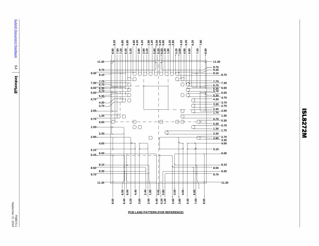
ISL8272M
54
FN8
67
0.1
September 17
, 2014
Subm
it Docum
ent Feedback
9.70
3.6
0
6.5
0
2.30
1.00
8.2
0
6.8
0
2.00
5.50
6.50
9.10
7.2
0
6.2
0
8.6
0
8.50
6.4
0
2.90
5.10
4.4
0
6.0
0
8.10
9.30
11.30
5.2
0
6.306.00
4.00
4.8
04
.20
3.8
03
.20
9.30
4.304.70
5.30
5.70
3.70
0.000.70
1.30
5.2
05
.80
7.306.70
7.8
0
8.8
0
9.70
7.70
6.30
11.30
2.0
0
5.4
0
7.0
0
0.2
00
.80
6.6
0
2.6
0
2.4
0
1.8
0
4.6
0
0.4
0
8.6
0
3.8
0
3.0
0
1.2
0
0.0
0
9.10
7.2
0
2.00
2.90
5.10
4.00
8.50
5.705.50
6.30 6.50
6.00
8.10
9.309.70
11.30
8.8
0
7.8
0
3.302.70
2.301.70
1.300.70
0.701.30
1.702.30
9.30
8.70
5.304.70
3.30
4.303.702.70
0.300.30
7.306.70
9.70
11.30
7.70
0.5
0
6.2
0
0.5
0
5.8
05
.20
4.8
04
.20
3.8
03
.20
2.8
0.2
.20
.
1.2
00
.80
0.8
01
.20
1.8
02
.20
0.2
00
.20
2.8
0
1.8
0
PCB LAND PATTERN (FOR REFERENCE)
PCB layout pattern