See Datasheet PDF - TI.com · 22uF 1.8V / 1A 10uF 2.2µH TPS62161 VIN EN AGND PGND SW VOS PG FB...
40
22uF 1.8V / 1A 10uF 2.2μH TPS62161 VIN EN AGND PGND SW VOS PG FB 100k (3 .. 17)V Product Folder Order Now Technical Documents Tools & Software Support & Community Reference Design An IMPORTANT NOTICE at the end of this data sheet addresses availability, warranty, changes, use in safety-critical applications, intellectual property matters and other important disclaimers. PRODUCTION DATA. TPS62160, TPS62161, TPS62162, TPS62163 SLVSAM2E – NOVEMBER 2011 – REVISED MAY 2017 TPS6216x 3-V to 17-V, 1-A Step-Down Converters with DCS-Control™ 1 1 Features 1• DCS-Control™ Topology • Input Voltage Range from 3 V to 17 V • Up to 1-A Output Current • Adjustable Output Voltage From 0.9 V to 6 V • Fixed Output Voltage Versions • Seamless Power Save Mode Transition • Typically 17-μA Quiescent Current • Power Good Output • 100% Duty Cycle Mode • Short Circuit Protection • Over Temperature Protection • Pin to Pin Compatible With TPS62170 and TPS62125 • Available in 3.00 mm x 3.00 mm 8-Pin VSSOP and 2.00 mm × 2.00 mm 8-Pin WSON Packages • Create a Custom Design using the TPS62160 with the WEBENCH® Power Designer 2 Applications • Standard 12-V Rail Supplies • POL Supply From Single or Multiple Li-Ion Battery • LDO Replacement • Embedded Systems • Digital Still Camera, Video • Mobile PCs, Tablet-PCs, Modems 3 Description The TPS6216x device family are easy to use synchronous step-down DC/DC converters optimized for applications with high power density. A high switching frequency of typically 2.25 MHz allows the use of small inductors and provides fast transient response as well as high output voltage accuracy by utilization of the DCS-Control™ topology. With its wide operating input voltage range of 3 V to 17 V, the devices are ideally suited for systems powered from either a Li-Ion or other battery as well as from 12-V intermediate power rails. It supports up to 1-A continuous output current at output voltages between 0.9 V and 6 V (with 100% duty cycle mode). Power sequencing is also possible by configuring the enable and open-drain power good pins. In power save mode, the devices show quiescent current of about 17 μA from VIN. Power save mode, entered automatically and seamlessly if the load is small, maintains high efficiency over the entire load range. In shutdown mode, the device is turned off and shutdown current consumption is less than 2 μA. The device, available in adjustable and fixed output voltage versions, is packaged in an 8-pin WSON package measuring 2.00 mm × 2.00 mm (DSG) or 8- pin VSSOP package measuring 3.00 mm x 3.00 mm (DGK). Device Information (1) PART NUMBER PACKAGE BODY SIZE (NOM) TPS6216x WSON (8) 2.00 mm x 2.00 mm TPS62160 VSSOP (8) 3.00 mm x 3.00 mm (1) For all available packages, see the orderable addendum at the end of the datasheet. Typical Application Schematic Efficiency vs Output Current
Transcript of See Datasheet PDF - TI.com · 22uF 1.8V / 1A 10uF 2.2µH TPS62161 VIN EN AGND PGND SW VOS PG FB...

22uF
1.8V / 1A
10uF
2.2µH
TPS62161
VIN
EN
AGND
PGND
SW
VOS
PG
FB
100k
(3 .. 17)V
Product
Folder
Order
Now
Technical
Documents
Tools &
Software
Support &Community
ReferenceDesign
An IMPORTANT NOTICE at the end of this data sheet addresses availability, warranty, changes, use in safety-critical applications,intellectual property matters and other important disclaimers. PRODUCTION DATA.
TPS62160, TPS62161, TPS62162, TPS62163SLVSAM2E –NOVEMBER 2011–REVISED MAY 2017
TPS6216x 3-V to 17-V, 1-A Step-Down Converters with DCS-Control™
1
1 Features1• DCS-Control™ Topology• Input Voltage Range from 3 V to 17 V• Up to 1-A Output Current• Adjustable Output Voltage From 0.9 V to 6 V• Fixed Output Voltage Versions• Seamless Power Save Mode Transition• Typically 17-µA Quiescent Current• Power Good Output• 100% Duty Cycle Mode• Short Circuit Protection• Over Temperature Protection• Pin to Pin Compatible With TPS62170 and
TPS62125• Available in 3.00 mm x 3.00 mm 8-Pin VSSOP
and 2.00 mm × 2.00 mm 8-Pin WSON Packages• Create a Custom Design using the TPS62160 with
the WEBENCH® Power Designer
2 Applications• Standard 12-V Rail Supplies• POL Supply From Single or Multiple Li-Ion Battery• LDO Replacement• Embedded Systems• Digital Still Camera, Video• Mobile PCs, Tablet-PCs, Modems
3 DescriptionThe TPS6216x device family are easy to usesynchronous step-down DC/DC converters optimizedfor applications with high power density. A highswitching frequency of typically 2.25 MHz allows theuse of small inductors and provides fast transientresponse as well as high output voltage accuracy byutilization of the DCS-Control™ topology.
With its wide operating input voltage range of 3 V to17 V, the devices are ideally suited for systemspowered from either a Li-Ion or other battery as wellas from 12-V intermediate power rails. It supports upto 1-A continuous output current at output voltagesbetween 0.9 V and 6 V (with 100% duty cycle mode).
Power sequencing is also possible by configuring theenable and open-drain power good pins.
In power save mode, the devices show quiescentcurrent of about 17 μA from VIN. Power save mode,entered automatically and seamlessly if the load issmall, maintains high efficiency over the entire loadrange. In shutdown mode, the device is turned offand shutdown current consumption is less than 2 μA.
The device, available in adjustable and fixed outputvoltage versions, is packaged in an 8-pin WSONpackage measuring 2.00 mm × 2.00 mm (DSG) or 8-pin VSSOP package measuring 3.00 mm x 3.00 mm(DGK).
Device Information(1)
PART NUMBER PACKAGE BODY SIZE (NOM)TPS6216x WSON (8) 2.00 mm x 2.00 mmTPS62160 VSSOP (8) 3.00 mm x 3.00 mm
(1) For all available packages, see the orderable addendum atthe end of the datasheet.
Typical Application Schematic Efficiency vs Output Current

2
TPS62160, TPS62161, TPS62162, TPS62163SLVSAM2E –NOVEMBER 2011–REVISED MAY 2017 www.ti.com
Product Folder Links: TPS62160 TPS62161 TPS62162 TPS62163
Submit Documentation Feedback Copyright © 2011–2017, Texas Instruments Incorporated
Table of Contents1 Features .................................................................. 12 Applications ........................................................... 13 Description ............................................................. 14 Revision History..................................................... 25 Device Voltage Options......................................... 46 Pin Configuration and Functions ......................... 47 Specifications......................................................... 5
7.1 Absolute Maximum Ratings ...................................... 57.2 ESD Ratings ............................................................ 57.3 Recommended Operating Conditions....................... 57.4 Thermal Information ................................................. 57.5 Electrical Characteristics........................................... 67.6 Typical Characteristics .............................................. 7
8 Detailed Description .............................................. 88.1 Overview ................................................................... 88.2 Functional Block Diagrams ....................................... 88.3 Feature Description................................................... 98.4 Device Functional Modes........................................ 11
9 Application and Implementation ........................ 13
9.1 Application Information............................................ 139.2 Typical Application ................................................. 139.3 System Examples ................................................... 23
10 Power Supply Recommendations ..................... 2511 Layout................................................................... 26
11.1 Layout Guidelines ................................................. 2611.2 Layout Example .................................................... 2611.3 Thermal Considerations ........................................ 27
12 Device and Documentation Support ................. 2812.1 Custom Design With WEBENCH® Tools ............. 2812.2 Device Support .................................................... 2812.3 Documentation Support ........................................ 2812.4 Related Links ........................................................ 2812.5 Community Resources.......................................... 2812.6 Trademarks ........................................................... 2912.7 Electrostatic Discharge Caution............................ 2912.8 Glossary ................................................................ 29
13 Mechanical, Packaging, and OrderableInformation ........................................................... 29
4 Revision HistoryNOTE: Page numbers for previous revisions may differ from page numbers in the current version.
Changes from Revision D (October 2014) to Revision E Page
• Added link to WEBENCH® Designer .................................................................................................................................... 1• Added "SW (AC), less than 10ns" specification to Absolute Maximum Ratings table ........................................................... 5• Changed TJ MAX spec from "125" to "150" ........................................................................................................................... 5• Added IQ and ISD specifications .............................................................................................................................................. 6• Added 125°C plot line in Figure 1 and Figure 4 Typical Characteristics graphic entities. .................................................... 7
Changes from Revision C (September 2013) to Revision D Page
• Added Device Information and ESD Ratings tables, Feature Description section, Device Functional Modes,Application and Implementation section, Power Supply Recommendations section, Layout section, Device andDocumentation Support section, and Mechanical, Packaging, and Orderable Information section....................................... 1
Changes from Revision B (August 2013) to Revision C Page
• Changed 50mV/μs to 50mV/s in Enable / Shutdown (EN) section ....................................................................................... 9
Changes from Revision A (March 2012) to Revision B Page
• Added note to Terminal Functions.......................................................................................................................................... 4• Changed Equation 13........................................................................................................................................................... 25• Added diode to Figure 41 ..................................................................................................................................................... 25

3
TPS62160, TPS62161, TPS62162, TPS62163www.ti.com SLVSAM2E –NOVEMBER 2011–REVISED MAY 2017
Product Folder Links: TPS62160 TPS62161 TPS62162 TPS62163
Submit Documentation FeedbackCopyright © 2011–2017, Texas Instruments Incorporated
Changes from Original (November 2011) to Revision A Page
• Changed data sheet from mixed status to production data.................................................................................................... 1• Added VSSOP-8 package to Features................................................................................................................................... 1• Added 8-pin VSSOP package to Description ......................................................................................................................... 1• Added DGK package pinout ................................................................................................................................................... 4• Added DGK package to Thermal Information ....................................................................................................................... 5• Changed Table 2 .................................................................................................................................................................. 14
1
2
3
4
8
7
6
5
PGND
VIN
EN
AGND
PG
SW
VOS
FB
PG
SW
VOS
FB
Exposed
Thermal
Pad
PGND
VIN
EN
AGND
7
6
2
3
1
4
8
5
4
TPS62160, TPS62161, TPS62162, TPS62163SLVSAM2E –NOVEMBER 2011–REVISED MAY 2017 www.ti.com
Product Folder Links: TPS62160 TPS62161 TPS62162 TPS62163
Submit Documentation Feedback Copyright © 2011–2017, Texas Instruments Incorporated
(1) Contact the factory to check availability of other fixed output voltage versions.
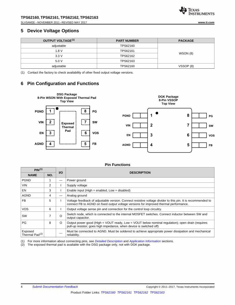
5 Device Voltage Options
OUTPUT VOLTAGE (1) PART NUMBER PACKAGEadjustable TPS62160
WSON (8)1.8 V TPS621613.3 V TPS621625.0 V TPS62163
adjustable TPS62160 VSSOP (8)
6 Pin Configuration and Functions
DSG Package8-Pin WSON With Exposed Thermal Pad
Top ViewDGK Package8-Pin VSSOP
Top View
SPACE
(1) For more information about connecting pins, see Detailed Description and Application Information sections.(2) The exposed thermal pad is available with the DSG package only, not with DGK package.
Pin FunctionsPIN (1)
I/O DESCRIPTIONNAME NO.
PGND 1 — Power groundVIN 2 I Supply voltageEN 3 I Enable input (High = enabled, Low = disabled)AGND 4 — Analog groundFB 5 I Voltage feedback of adjustable version. Connect resistive voltage divider to this pin. It is recommended to
connect FB to AGND on fixed output voltage versions for improved thermal performance.VOS 6 I Output voltage sense pin and connection for the control loop circuitry.
SW 7 O Switch node, which is connected to the internal MOSFET switches. Connect inductor between SW andoutput capacitor.
PG 8 O Output power good (High = VOUT ready, Low = VOUT below nominal regulation); open drain (requirespull-up resistor; goes high impedance, when device is switched off)
ExposedThermal Pad (2) — Must be connected to AGND. Must be soldered to achieve appropriate power dissipation and mechanical
reliability.

5
TPS62160, TPS62161, TPS62162, TPS62163www.ti.com SLVSAM2E –NOVEMBER 2011–REVISED MAY 2017
Product Folder Links: TPS62160 TPS62161 TPS62162 TPS62163
Submit Documentation FeedbackCopyright © 2011–2017, Texas Instruments Incorporated
(1) Stresses beyond those listed under Absolute Maximum Ratings may cause permanent damage to the device. These are stress ratingsonly, which do not imply functional operation of the device at these or any other conditions beyond those indicated under RecommendedOperating Conditions. Exposure to absolute-maximum-rated conditions for extended periods may affect device reliability.
(2) All voltages are with respect to network ground terminal.(3) While switching.
7 Specifications
7.1 Absolute Maximum Ratings (1)
MIN MAX UNIT
Pin voltage range (2)
VIN –0.3 20 VEN, SW (DC) –0.3 VIN + 0.3
VSW (AC), less than 10ns (3) –2 24.5FB, PG, VOS –0.3 7 V
Power good sink current PG 10 mAOperating junction temperature, TJ –40 150 °CStorage temperature, Tstg –65 150 °C
(1) JEDEC document JEP155 states that 500-V HBM allows safe manufacturing with a standard ESD control process.(2) JEDEC document JEP157 states that 250-V CDM allows safe manufacturing with a standard ESD control process.
7.2 ESD RatingsVALUE UNIT
V(ESD) Electrostatic dischargeHuman body model (HBM), per ANSI/ESDA/JEDEC JS-001, all pins (1) ±2000
VCharged device model (CDM), per JEDEC specification JESD22-C101,all pins (2) ±500
7.3 Recommended Operating ConditionsMIN NOM MAX UNIT
Supply Voltage, VIN 3 17 VOutput Voltage, VOUT 0.9 6 VOperating junction temperature, TJ –40 125 °C
(1) For more information about traditional and new thermal metrics, see the Semiconductor and IC Package Thermal Metrics applicationreport, SPRA953.
7.4 Thermal Information
THERMAL METRIC (1)TPS6216X
UNITDSG (WSON) DGK (VSSOP)8 PINS 8 PINS
RθJA Junction-to-ambient thermal resistance 61.8 184.3 °C/WRθJC(top) Junction-to-case (top) thermal resistance 61.3 74.6 °C/WRθJB Junction-to-board thermal resistance 15.5 105.8 °C/WψJT Junction-to-top characterization parameter 0.4 13.3 °C/WψJB Junction-to-board characterization parameter 15.4 104.2 °C/WRθJC(bot) Junction-to-case (bottom) thermal resistance 8.6 — °C/W

6
TPS62160, TPS62161, TPS62162, TPS62163SLVSAM2E –NOVEMBER 2011–REVISED MAY 2017 www.ti.com
Product Folder Links: TPS62160 TPS62161 TPS62162 TPS62163
Submit Documentation Feedback Copyright © 2011–2017, Texas Instruments Incorporated
(1) The device is still functional down to under voltage lockout (see parameter VUVLO).(2) Current into VIN pin.(3) This is the static current limit. It can be temporarily higher in applications due to internal propagation delay (see Current Limit and Short
Circuit Protection section).(4) This is the voltage regulated at the FB pin.(5) This is the accuracy provided by the device itself (line and load regulation effects are not included). For fixed voltage versions, the
(internal) resistive feedback divider is included.(6) Line and load regulation are depending on external component selection and layout (see Figure 18 and Figure 19).
7.5 Electrical CharacteristicsOver junction temperature range (TJ = –40°C to +125°C), typical values at VIN = 12 V and TJ = 25°C (unless otherwise noted)
PARAMETER TEST CONDITIONS MIN TYP MAX UNITSUPPLYVIN Input voltage range (1) 3 17 V
IQ Operating quiescent currentEN = High, IOUT = 0 mA,device not switching
17 30µA
TJ = -40°C to +85°C 17 25ISD Shutdown current (2) EN = Low
1.5 25µA
TJ = -40°C to +85°C 1.5 4
VUVLOUndervoltage lockoutthreshold
Falling input voltage 2.6 2.7 2.82 VHysteresis 180 mV
TSD
Thermal shutdowntemperature Rising temperature 160
°CThermal shutdown hysteresis Falling temperature 20
CONTROL (EN, PG)
VEN_HHigh level input thresholdvoltage (EN) 0.9 0.6 V
VEN_L Low level input thresholdvoltage (EN)
0.56 0.3 V
ILKG_EN Input leakage current (EN) EN = VIN or GND 0.01 1 µA
VTH_PGPower good thresholdvoltage
Rising (%VOUT) 92% 95% 98%Falling (%VOUT) 87% 90% 93%
VOL_PGPower good output lowvoltage IPG = –2 mA 0.07 0.3 V
ILKG_PG Input leakage current (PG) VPG = 1.8 V 1 400 nAPOWER SWITCH
RDS(ON)
High-side MOSFET ON-resistance
VIN ≥ 6 V 300 600mΩ
VIN = 3 V 430
Low-side MOSFET ON-resistance
VIN ≥ 6 V 120 200mΩ
VIN = 3 V 165
ILIMFHigh-side MOSFET forwardcurrent limit (3)
VIN = 12 V, TJ = 25°C 1.45 1.95 2.45 A
OUTPUTVREF Internal reference voltage (4) 0.8 VILKG_FB Pin leakage current (FB) TPS62160, VFB = 1.2 V 5 400 nA
VOUT
Output voltage range(TPS62160) VIN ≥ VOUT 0.9 6.0 V
Initial output voltageaccuracy (5)
PWM mode operation, VIN ≥ VOUT + 1 V –3% 3%Power save mode operation, COUT = 22 µF –3.5% 4%
DC output voltage loadregulation (6) VIN = 12 V, VOUT = 3.3 V, PWM mode operation 0.05 %/A
DC output voltage lineregulation (6)
3 V ≤ VIN ≤ 17 V, VOUT = 3.3 V, IOUT = 0.5 A, PWM modeoperation 0.02 %/V
0.0
50.0
100.0
150.0
200.0
250.0
300.0
350.0
400.0
450.0
500.0
550.0
600.0
3.0 6.0 9.0 12.0 15.0 18.0
−40°C
−20°C
25°C
85°C
125°C
Input Voltage (V)
RD
Son
Hig
h−S
ide
(mΩ
)
G001
0.0
25.0
50.0
75.0
100.0
125.0
150.0
175.0
200.0
225.0
250.0
3.0 6.0 9.0 12.0 15.0 18.0 20.0
−40°C
−20°C
25°C
85°C125°C
Input Voltage (V)
RD
Son
Low
−S
ide
(mΩ
)
G001
7
TPS62160, TPS62161, TPS62162, TPS62163www.ti.com SLVSAM2E –NOVEMBER 2011–REVISED MAY 2017
Product Folder Links: TPS62160 TPS62161 TPS62162 TPS62163
Submit Documentation FeedbackCopyright © 2011–2017, Texas Instruments Incorporated
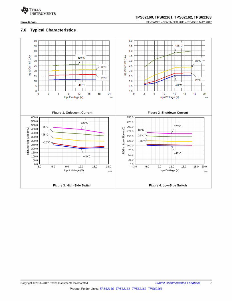
7.6 Typical Characteristics
Figure 1. Quiescent Current Figure 2. Shutdown Current
Figure 3. High-Side Switch Figure 4. Low-Side Switch
control logic
Soft
start
Thermal
ShtdwnUVLO PG control
power
control
error
amplifier
gate
drive
HS lim
LS lim
VINPG
PGNDAGND
comp
comp
+
_timer tON
DCS - ControlTM
direct control
&
compensation
comparator
ramp
SWEN*
VOS
FB
*This pin is connected to a pull down resistor internally
(see Detailed Description section).
8
TPS62160, TPS62161, TPS62162, TPS62163SLVSAM2E –NOVEMBER 2011–REVISED MAY 2017 www.ti.com
Product Folder Links: TPS62160 TPS62161 TPS62162 TPS62163
Submit Documentation Feedback Copyright © 2011–2017, Texas Instruments Incorporated
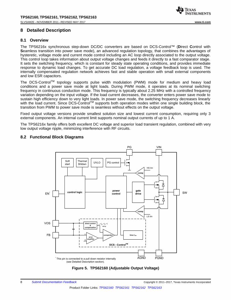
8 Detailed Description
8.1 OverviewThe TPS6216x synchronous step-down DC/DC converters are based on DCS-Control™ (Direct Control withSeamless transition into power save mode), an advanced regulation topology, that combines the advantages ofhysteretic, voltage mode and current mode control including an AC loop directly associated to the output voltage.This control loop takes information about output voltage changes and feeds it directly to a fast comparator stage.It sets the switching frequency, which is constant for steady state operating conditions, and provides immediateresponse to dynamic load changes. To get accurate DC load regulation, a voltage feedback loop is used. Theinternally compensated regulation network achieves fast and stable operation with small external componentsand low ESR capacitors.
The DCS-ControlTM topology supports pulse width modulation (PWM) mode for medium and heavy loadconditions and a power save mode at light loads. During PWM mode, it operates at its nominal switchingfrequency in continuous conduction mode. This frequency is typically about 2.25 MHz with a controlled frequencyvariation depending on the input voltage. If the load current decreases, the converter enters power save mode tosustain high efficiency down to very light loads. In power save mode, the switching frequency decreases linearlywith the load current. Since DCS-ControlTM supports both operation modes within one single building block, thetransition from PWM to power save mode is seamless without effects on the output voltage.
Fixed output voltage versions provide smallest solution size and lowest current consumption, requiring only 3external components. An internal current limit supports nominal output currents of up to 1 A.
The TPS6216x family offers both excellent DC voltage and superior load transient regulation, combined with verylow output voltage ripple, minimizing interference with RF circuits.
8.2 Functional Block Diagrams
Figure 5. TPS62160 (Adjustable Output Voltage)

control logic
Soft
start
Thermal
ShtdwnUVLO PG control
power
control
error
amplifier
gate
drive
HS lim
LS lim
VINPG
PGNDAGND
comp
comp
+
_timer tON
DCS - ControlTM
direct control
&
compensation
comparator
ramp
SWEN*
VOS
FB*
*This pin is connected to a pull down resistor internally
(see Detailed Description section).
9
TPS62160, TPS62161, TPS62162, TPS62163www.ti.com SLVSAM2E –NOVEMBER 2011–REVISED MAY 2017
Product Folder Links: TPS62160 TPS62161 TPS62162 TPS62163
Submit Documentation FeedbackCopyright © 2011–2017, Texas Instruments Incorporated
Functional Block Diagrams (continued)
Figure 6. TPS62161/TPS62162/TPS62163 (Fixed Output Voltage)
8.3 Feature Description
8.3.1 Enable and Shutdown (EN)When enable (EN) is set high, the device starts operation.
Shutdown is forced if EN is pulled low with a shutdown current of typically 1.5 µA. During shutdown, the internalpower MOSFETs as well as the entire control circuitry are turned off. The internal resistive divider pulls down theoutput voltage smoothly. If the EN pin is low, an internal pull-down resistor of about 400 kΩ is connected andkeeps it low, to avoid bouncing.
Connecting the EN pin to an appropriate output signal of another power rail provides sequencing of multiplepower rails.
8.3.2 Current Limit and Short Circuit ProtectionThe TPS6216x devices are protected against heavy load and short circuit events. At heavy loads, the currentlimit determines the maximum output current. If the current limit is reached, the high-side FET is turned off.Avoiding shoot through current, the low-side FET is switched on to allow the inductor current to decrease. Thehigh-side FET turns on again, only if the current in the low-side FET decreases below the low-side current limitthreshold of typically 1.2 A.
The output current of the device is limited by the current limit (see Electrical Characteristics). Due to internalpropagation delay, the actual current can exceed the static current limit during that time. The dynamic currentlimit is calculated as follows:
space

( )ns
L
VVII OUTIN
LIMFtyppeak 30)( ×-
+=
PD
L
LIMFtyppeak tL
VII ×+=)(
10
TPS62160, TPS62161, TPS62162, TPS62163SLVSAM2E –NOVEMBER 2011–REVISED MAY 2017 www.ti.com
Product Folder Links: TPS62160 TPS62161 TPS62162 TPS62163
Submit Documentation Feedback Copyright © 2011–2017, Texas Instruments Incorporated
Feature Description (continued)
where• ILIMF is the static current limit, specified in Electrical Characteristics• L is the inductor value• VL is the voltage across the inductor• tPD is the internal propagation delay (1)
space
The dynamic high-side switch peak current is calculated as follows:
space
(2)
space
Take care with the current limit, if the input voltage is high and very small inductances are used.
8.3.3 Power Good (PG)The TPS6216x has a built in power good (PG) function to indicate whether the output voltage has reached itsappropriate level or not. The PG signal can be used for startup sequencing of multiple rails. The PG pin is anopen-drain output that requires a pull-up resistor (to any voltage below 7 V). It can sink 2 mA of current andmaintain its specified logic low level. It is high impedance when the device is turned off due to EN, UVLO orthermal shutdown. If not used, the PG pin should be connected to GND but may be left floating.
space
Table 1. Power Good Pin Logic Table
Device StatePG Logic Status
High Impedance Low
Enable (EN=High)VFB ≥ VTH_PG √VFB ≤ VTH_PG √
Shutdown (EN=Low) √UVLO 0.7 V < VIN < VUVLO √Thermal Shutdown TJ > TSD √Power Supply Removal VIN < 0.7 V √
space
8.3.4 Undervoltage Lockout (UVLO)If the input voltage drops, the under voltage lockout prevents misoperation of the device by switching off both thepower FETs. The under voltage lockout threshold is set typically to 2.7 V. The device is fully operational forvoltages above the UVLO threshold and turns off if the input voltage trips the threshold. The converter startsoperation again once the input voltage exceeds the threshold by a hysteresis of typically 180 mV.
8.3.5 Thermal ShutdownThe junction temperature (TJ) of the device is monitored by an internal temperature sensor. If TJ exceeds 160°C(typical), the device goes into thermal shut down. Both the high-side and low-side power FETs are turned off andPG goes high impedance. When TJ decreases below the hysteresis amount, the converter resumes normaloperation, beginning with soft start. To avoid unstable conditions, a hysteresis of typically 20°C is implementedon the thermal shut down temperature.
ON
OUTIN
peakLPSM tL
VVI ×
-
=
)()(
nsV
Vt
IN
OUT
ON420×=
11
TPS62160, TPS62161, TPS62162, TPS62163www.ti.com SLVSAM2E –NOVEMBER 2011–REVISED MAY 2017
Product Folder Links: TPS62160 TPS62161 TPS62162 TPS62163
Submit Documentation FeedbackCopyright © 2011–2017, Texas Instruments Incorporated
8.4 Device Functional Modes
8.4.1 Soft StartThe internal soft start circuitry controls the output voltage slope during startup. This avoids excessive inrushcurrent and ensures a controlled output voltage rise time. It also prevents unwanted voltage drops from high-impedance power sources or batteries. When EN is set to start device operation, the device starts switching aftera delay of about 50 µs and VOUT rises with a slope of about 25 mV/µs. See Figure 30 and Figure 31 for typicalstartup operation.
The TPS6216x can start into a pre-biased output. During monotonic pre-biased startup, the low-side MOSFET isnot allowed to turn on until the device's internal ramp sets an output voltage above the pre-bias voltage.
8.4.2 Pulse Width Modulation (PWM) OperationThe TPS6216x operates with pulse width modulation in continuous conduction mode (CCM) with a nominalswitching frequency of about 2.25 MHz. The frequency variation in PWM is controlled and depends on VIN, VOUTand the inductance. The device operates in PWM mode as long the output current is higher than half theinductor's ripple current. To maintain high efficiency at light loads, the device enters power save mode at theboundary to discontinuous conduction mode (DCM). This happens if the output current becomes smaller thanhalf the inductor's ripple current.
8.4.3 Power Save Mode OperationThe TPS6216x's built in power save mode is entered seamlessly, if the load current decreases. This secures ahigh efficiency in light load operation. The device remains in power save mode as long as the inductor current isdiscontinuous.
In power save mode the switching frequency decreases linearly with the load current maintaining high efficiency.The transition into and out of power save mode happens within the entire regulation scheme and is seamless inboth directions.
The TPS6216x includes a fixed on-time circuitry. This on-time, in steady-state operation, is estimated as:
space
(3)
space
For very small output voltages, the on-time increases beyond the result of Equation 3, to stay above an absoluteminimum on-time, tON(min), which is around 80 ns, to limit switching losses. The peak inductor current in PSM isapproximated by:
space
(4)
space
When VIN decreases to typically 15% above VOUT, the TPS6216x does not enter power save mode, regardless ofthe load current. The device maintains output regulation in PWM mode.
8.4.4 100% Duty-Cycle OperationThe duty cycle of the buck converter is given by D = VOUT/VIN and increases as the input voltage comes close tothe output voltage. In this case, the device starts 100% duty cycle operation turning on the high-side switch100% of the time. The high-side switch stays turned on as long as the output voltage is below the internalsetpoint. This allows the conversion of small input to output voltage differences, such as for longest operationtime of battery-powered applications. In 100% duty cycle mode, the low-side FET is switched off.
The minimum input voltage to maintain output voltage regulation, depending on the load current and the outputvoltage level, is calculated as:

( )L)on(DSOUT(min)OUT(min)IN RRIVV ++=
12
TPS62160, TPS62161, TPS62162, TPS62163SLVSAM2E –NOVEMBER 2011–REVISED MAY 2017 www.ti.com
Product Folder Links: TPS62160 TPS62161 TPS62162 TPS62163
Submit Documentation Feedback Copyright © 2011–2017, Texas Instruments Incorporated
Device Functional Modes (continued)space
where• IOUT is the output current• RDS(on) is the RDS(on) of the high-side FET• RL is the DC resistance of the inductor used (5)

C1
VIN
TPS62160
VIN
EN
AGND
PGND
SW
VOS
PG
FB
C2
2.2µH
R1
R2
R3
VOUT
13
TPS62160, TPS62161, TPS62162, TPS62163www.ti.com SLVSAM2E –NOVEMBER 2011–REVISED MAY 2017
Product Folder Links: TPS62160 TPS62161 TPS62162 TPS62163
Submit Documentation FeedbackCopyright © 2011–2017, Texas Instruments Incorporated
9 Application and Implementation
NOTEInformation in the following applications sections is not part of the TI componentspecification, and TI does not warrant its accuracy or completeness. TI’s customers areresponsible for determining suitability of components for their purposes. Customers shouldvalidate and test their design implementation to confirm system functionality.
9.1 Application InformationThe TPS6216x device family are easy to use synchronous step-down DC/DC converters optimized forapplications with high power density. A high switching frequency of typically 2.25 MHz allows the use of smallinductors and provides fast transient response as well as high output voltage accuracy by utilization of the DCS-Control™ topology. With its wide operating input voltage range of 3 V to 17 V, the devices are ideally suited forsystems powered from either a Li-Ion or other battery as well as from 12-V intermediate power rails. It supportsup to 1-A continuous output current at output voltages between 0.9 V and 6 V (with 100% duty cycle mode).
9.2 Typical ApplicationSPACE
Figure 7. TPS62160 Adjustable Power Supply
space
9.2.1 Design RequirementsThe design guideline provides a component selection to operate the device within the Recommended OperatingConditions.
9.2.2 Detailed Design Procedure
9.2.2.1 Custom Design with WEBENCH® ToolsClick here to create a custom design using the TPS62160 device with the WEBENCH® Power Designer.1. Start by entering your VIN, VOUT, and IOUT requirements.2. Optimize your design for key parameters like efficiency, footprint and cost using the optimizer dial and
compare this design with other possible solutions from Texas Instruments.3. The WEBENCH Power Designer provides you with a customized schematic along with a list of materials with
real time pricing and component availability.4. In most cases, you will also be able to:
– Run electrical simulations to see important waveforms and circuit performance– Run thermal simulations to understand the thermal performance of your board– Export your customized schematic and layout into popular CAD formats– Print PDF reports for the design, and share your design with colleagues
5. Get more information about WEBENCH tools at www.ti.com/WEBENCH.
2
III
(m ax)L(m ax)OUT(m ax)L
D+=
÷ø
öçè
æ-= 1
0.8V
VRR
OUT21
14
TPS62160, TPS62161, TPS62162, TPS62163SLVSAM2E –NOVEMBER 2011–REVISED MAY 2017 www.ti.com
Product Folder Links: TPS62160 TPS62161 TPS62162 TPS62163
Submit Documentation Feedback Copyright © 2011–2017, Texas Instruments Incorporated
Typical Application (continued)
(1) The values in the table are nominal values. Variations of typically ±20% due to tolerance, saturation and DC bias are assumed.(2) This LC combination is the standard value and recommended for most applications.
9.2.2.2 Programming the Output VoltageWhile the output voltage of the TPS62160 is adjustable, the TPS62161/TPS62162/TPS62163 are programmed tofixed output voltages. For fixed output versions, the FB pin is pulled down internally and may be left floating. It isrecommended to connect it to AGND to improve thermal resistance. The adjustable version can be programmedfor output voltages from 0.9 V to 6 V by using a resistive divider from VOUT to AGND. The voltage at the FB pinis regulated to 800 mV. The value of the output voltage is set by the selection of the resistive divider fromEquation 6. It is recommended to choose resistor values which allow a current of at least 2 µA, meaning thevalue of R2 should not exceed 400 kΩ. Lower resistor values are recommended for highest accuracy and mostrobust design. For applications requiring lowest current consumption, the use of fixed output voltage versions isrecommended.
spacing
(6)
spacing
If the FB pin becomes open, the device clamps the output voltage at the VOS pin to about 7.4 V.
9.2.2.3 External Component SelectionThe external components have to fulfill the needs of the application, but also the stability criteria of the devicescontrol loop. The TPS6216x is optimized to work within a range of external components. The LC output filter'sinductance and capacitance have to be considered together, creating a double pole, responsible for the cornerfrequency of the converter (see Output Filter and Loop Stability section). Table 2 can be used to simplify theoutput filter component selection. Checked cells represent combinations that are proven for stability by simulationand lab test. Further combinations should be checked for each individual application.
space
Table 2. Recommended LC Output Filter Combinations (1)
4.7µF 10µF 22µF 47µF 100µF 200µF 400µF1µH
2.2µH √ √ (2) √ √ √3.3µH √ √ √ √4.7µH
space
More detailed information on further LC combinations can be found in SLVA463.
9.2.2.4 Inductor SelectionThe inductor selection is affected by several effects like inductor ripple current, output ripple voltage, PWM-to-PSM transition point and efficiency. In addition, the inductor selected has to be rated for appropriate saturationcurrent and DC resistance (DCR). Equation 7 and Equation 8 calculate the maximum inductor current understatic load conditions.
spacing
(7)
spacing
spacing

LPSMloadII D=
2
1
)(
÷÷÷÷÷
ø
ö
ççççç
è
æ
×
-
×=DSW
IN
OUT
OUTLfL
V
V
VI(min)
(max)
(max)
1
15
TPS62160, TPS62161, TPS62162, TPS62163www.ti.com SLVSAM2E –NOVEMBER 2011–REVISED MAY 2017
Product Folder Links: TPS62160 TPS62161 TPS62162 TPS62163
Submit Documentation FeedbackCopyright © 2011–2017, Texas Instruments Incorporated
(1) See the Third-Party Products Disclaimer.(2) IRMS at 40°C rise or ISAT at 30% drop.
where• IL(max) is the maximum inductor current• ΔIL is the peak-to-peak inductor ripple current• L(min) is the minimum effective inductor value• fSW is the actual PWM switching frequency (8)
spacing
Calculating the maximum inductor current using the actual operating conditions gives the minimum saturationcurrent of the inductor needed. A margin of about 20% is recommended to add. A larger inductor value is alsouseful to get lower ripple current, but increases the transient response time and size as well. The followinginductors have been used with the TPS6216x and are recommended for use:
Table 3. List of Inductors (1)
Type Inductance [µH] Current [A] (2) Dimensions [L x B x H] mm ManufacturerVLF3012ST-2R2M1R4 2.2 µH, ±20% 1.9 A 3.0 x 2.8 x 1.2 TDKVLF302512MT-2R2M 2.2 µH, ±20% 1.9 A 3.0 x 2.5 x 1.2 TDK
VLS252012T-2R2M1R3 2.2 uH, ±20% 1.3 A 2.5 x 2.0 x 1.2 TDKXFL3012-222MEC 2.2 µH, ±20% 1.9 A 3.0 x 3.0 x 1.2 CoilcraftXFL3012-332MEC 3.3 µH, ±20% 1.6 A 3.0 x 3.0 x 1.2 CoilcraftLPS3015-332ML_ 3.3 uH, ±20% 1.4 A 3.0 x 3.0 x 1.4 CoilcraftNR3015T-2R2M 2.2 uH, ±20% 1.5 A 3.0 x 3.0 x 1.5 Taiyo Yuden
744025003 3.3 uH, ±20% 1.5 A 2.8 x 2.8 x 2.8 WuerthPSI25201B-2R2MS 2.2 uH, ±20% 1.3 A 2.0 x 2.5 x 1.2 Cyntec
The TPS6216x can operate with an inductor as low as 2.2 µH. However, for applications with low input voltages,3.3 µH is recommended to allow the full output current. The inductor value also determines the load current atwhich Power Save Mode is entered:
spacing
(9)
spacing
Using Equation 8, this current level is adjusted by changing the inductor value.
9.2.2.5 Capacitor Selection
9.2.2.5.1 Output Capacitor
The recommended value for the output capacitor is 22 uF. The architecture of the TPS6216x allows the use oftiny ceramic output capacitors with low equivalent series resistance (ESR). These capacitors provide low outputvoltage ripple and are recommended. To keep its low resistance up to high frequencies and to get narrowcapacitance variation with temperature, it is recommended to use an X7R or X5R dielectric. Using a higher valuecan have some advantages like smaller voltage ripple and a tighter DC output accuracy in power save mode(see SLVA463).
Note: In power save mode, the output voltage ripple depends on the output capacitance, its ESR and the peakinductor current. Using ceramic capacitors provides small ESR and low ripple.
÷÷ø
öççè
æ+×
×=
21
11
252
1
RRpFf pole
p
pFRf zero
252
1
1××
=
p
CLf LC
×
=
p2
1
16
TPS62160, TPS62161, TPS62162, TPS62163SLVSAM2E –NOVEMBER 2011–REVISED MAY 2017 www.ti.com
Product Folder Links: TPS62160 TPS62161 TPS62162 TPS62163
Submit Documentation Feedback Copyright © 2011–2017, Texas Instruments Incorporated
9.2.2.5.2 Input Capacitor
For most applications, 10 µF is sufficient and is recommended, though a larger value reduces input current ripplefurther. The input capacitor buffers the input voltage for transient events and also decouples the converter fromthe supply. A low ESR multilayer ceramic capacitor is recommended for best filtering and should be placedbetween VIN and PGND as close as possible to those pins.
spacing
NOTEDC bias effect: High capacitance ceramic capacitors have a DC bias effect, which has astrong influence on the final effective capacitance. Therefore the right capacitor value hasto be chosen carefully. Package size and voltage rating in combination with dielectricmaterial are responsible for differences between the rated capacitor value and theeffective capacitance.
spacing
9.2.2.6 Output Filter and Loop StabilityThe devices of the TPS6216x family are internally compensated to be stable with L-C filter combinationscorresponding to a corner frequency calculated with Equation 10:
spacing
(10)
spacing
Proven nominal values for inductance and ceramic capacitance are given in Table 2 and are recommended foruse. Different values may work, but care has to be taken on the loop stability which is affected. More informationincluding a detailed L-C stability matrix is found in SLVA463.
The TPS6216X devices, both fixed and adjustable versions, include an internal 25 pF feed forward capacitor,connected between the VOS and FB pins. This capacitor impacts the frequency behavior and sets a pole andzero in the control loop with the resistors of the feedback divider, per Equation 11 and Equation 12:
spacing
(11)
spacing
spacing
(12)
spacing
Though the TPS6216x devices are stable without the pole and zero being in a particular location, adjusting theirlocation to the specific needs of the application can provide better performance in power save mode and/orimproved transient response. An external feed-forward capacitor can also be added. A more detailed discussionon the optimization for stability versus transient response can be found in SLVA289 and SLVA466.
If using ceramic capacitors, the DC bias effect has to be considered. The DC bias effect results in a drop ineffective capacitance as the voltage across the capacitor increases (see NOTE in Input Capacitor section).
9.2.2.7 TPS6216x Components ListTable 4 shows the list of components for the Application Curves.
17
TPS62160, TPS62161, TPS62162, TPS62163www.ti.com SLVSAM2E –NOVEMBER 2011–REVISED MAY 2017
Product Folder Links: TPS62160 TPS62161 TPS62162 TPS62163
Submit Documentation FeedbackCopyright © 2011–2017, Texas Instruments Incorporated
Table 4. List of ComponentsREFERENCE DESCRIPTION MANUFACTURER
IC 17 V, 1 A Step-Down Converter, WSON TPS62160DSG, Texas InstrumentsL1 2.2 µH, 1.4 A, 3 mm x 2.8 mm x 1.2 mm VLF3012ST-2R2M1R4, TDKC1 10 µF, 25 V, Ceramic, 0805 StandardC2 22 µF, 6.3 V, Ceramic, 0805 StandardR1 depending on VOUT
R2 depending on VOUT
R3 100 kΩ, Chip, 0603, 1/16 W, 1% Standard
0.0
10.0
20.0
30.0
40.0
50.0
60.0
70.0
80.0
90.0
100.0
0.0001 0.001 0.01 0.1 1
VIN=5V
VIN=12V
VIN=17V
Output Current (A)
Effic
ien
cy (
%)
G001
0.0
10.0
20.0
30.0
40.0
50.0
60.0
70.0
80.0
90.0
100.0
4 5 6 7 8 9 10 11 12 13 14 15 16 17
IOUT=1mA IOUT=10mAIOUT=100mA
IOUT=1A
Input Voltage (V)
Effic
ien
cy (
%)
G001
0.0
10.0
20.0
30.0
40.0
50.0
60.0
70.0
80.0
90.0
100.0
0.0001 0.001 0.01 0.1 1
VIN=6V
VIN=12V
VIN=17V
Output Current (A)
Effi
cien
cy (
%)
VOUT=5.0VL=2.2uH (VLF3012ST)Cout=22uF
G001
0.0
10.0
20.0
30.0
40.0
50.0
60.0
70.0
80.0
90.0
100.0
7 8 9 10 11 12 13 14 15 16 17
IOUT=1mA
IOUT=10mA
IOUT=100mA
IOUT=1A
Input Voltage (V)
Effi
cien
cy (
%)
VOUT=5.0VL=2.2uH (VLF3012ST)Cout=22uF
G001
0.0
10.0
20.0
30.0
40.0
50.0
60.0
70.0
80.0
90.0
100.0
0.0001 0.001 0.01 0.1 1
VIN=6V
VIN=12V
VIN=17V
Output Current (A)
Effic
ien
cy (
%)
G001
0.0
10.0
20.0
30.0
40.0
50.0
60.0
70.0
80.0
90.0
100.0
7 8 9 10 11 12 13 14 15 16 17
IOUT=1mA
IOUT=10mA
IOUT=100mA
IOUT=1A
Input Voltage (V)
Effic
ien
cy (
%)
G001
18
TPS62160, TPS62161, TPS62162, TPS62163SLVSAM2E –NOVEMBER 2011–REVISED MAY 2017 www.ti.com
Product Folder Links: TPS62160 TPS62161 TPS62162 TPS62163
Submit Documentation Feedback Copyright © 2011–2017, Texas Instruments Incorporated
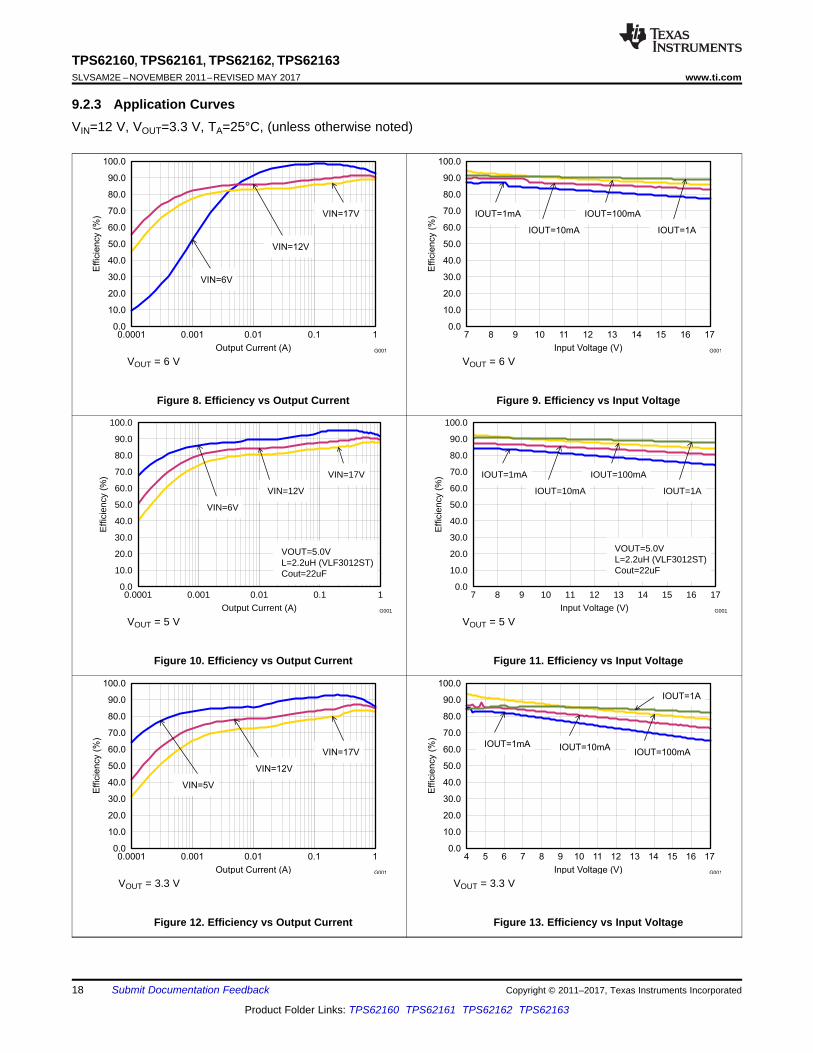
9.2.3 Application CurvesVIN=12 V, VOUT=3.3 V, TA=25°C, (unless otherwise noted)
VOUT = 6 V
Figure 8. Efficiency vs Output Current
VOUT = 6 V
Figure 9. Efficiency vs Input Voltage
VOUT = 5 V
Figure 10. Efficiency vs Output Current
VOUT = 5 V
Figure 11. Efficiency vs Input Voltage
VOUT = 3.3 V
Figure 12. Efficiency vs Output Current
VOUT = 3.3 V
Figure 13. Efficiency vs Input Voltage

3.20
3.25
3.30
3.35
0.0001 0.001 0.01 0.1 1
VIN=5V VIN=12VVIN=17V
Output Current (A)
Ou
tpu
t V
olta
ge
(V
)
G001
3.20
3.25
3.30
3.35
4 7 10 13 16
IOUT=1mA IOUT=10mA
IOUT=100mA IOUT=1A
Input Voltage (V)
Ou
tpu
t V
olta
ge
(V
)
G001
0.0
10.0
20.0
30.0
40.0
50.0
60.0
70.0
80.0
90.0
100.0
0.0001 0.001 0.01 0.1 1
VIN=5V
VIN=12V
VIN=17V
Output Current (A)
Effic
ien
cy (
%)
G001
0.0
10.0
20.0
30.0
40.0
50.0
60.0
70.0
80.0
90.0
100.0
3 4 5 6 7 8 9 10 11 12 13 14 15 16 17
IOUT=1mA
IOUT=10mAIOUT=100mA IOUT=1A
Input Voltage (V)
Effic
ien
cy (
%)
G001
0.0
10.0
20.0
30.0
40.0
50.0
60.0
70.0
80.0
90.0
100.0
0.0001 0.001 0.01 0.1 1
VIN=5V
VIN=12V
VIN=17V
Output Current (A)
Effic
ien
cy (
%)
G001
0.0
10.0
20.0
30.0
40.0
50.0
60.0
70.0
80.0
90.0
100.0
3 4 5 6 7 8 9 10 11 12 13 14 15 16 17
IOUT=1mAIOUT=10mA
IOUT=100mA
IOUT=500mA
Input Voltage (V)
Effic
ien
cy (
%)
G001
19
TPS62160, TPS62161, TPS62162, TPS62163www.ti.com SLVSAM2E –NOVEMBER 2011–REVISED MAY 2017
Product Folder Links: TPS62160 TPS62161 TPS62162 TPS62163
Submit Documentation FeedbackCopyright © 2011–2017, Texas Instruments Incorporated
VOUT = 1.8 V
Figure 14. Efficiency vs Output Current
VOUT = 1.8 V
Figure 15. Efficiency vs Input Voltage
VOUT = 0.9 V
Figure 16. Efficiency vs Output Current
VOUT = 0.9 V
Figure 17. Efficiency vs Input Voltage
Figure 18. Output Voltage Accuracy (Load Regulation) Figure 19. Output Voltage Accuracy (Line Regulation)
0
0.01
0.02
0.03
0.04
0.05
0 0.1 0.2 0.3 0.4 0.5 0.6 0.7 0.8 0.9 1
VIN=5V
VIN=12V
VIN=17V
Output Current (A)
Ou
tpu
t V
olta
ge
Rip
ple
(V
)
G000
0
0.5
1
1.5
2
2.5
3
4 5 6 7 8 9 10 11 12 13 14 15 16 17
−40°C 25°C
85°C
Input Voltage (V)
Ou
tpu
t C
urr
en
t (A
)
G000
0
0.5
1
1.5
2
2.5
3
3.5
4
0 0.1 0.2 0.3 0.4 0.5 0.6 0.7 0.8 0.9 1
Output Current (A)
Sw
itch
ing
Fre
qu
en
cy (
MH
z)
G000
0
0.5
1
1.5
2
2.5
3
3.5
4
4 6 8 10 12 14 16 18
IOUT=0.5A
IOUT=1A
Input Voltage (V)
Sw
itch
ing
Fre
qu
en
cy (
MH
z)
G000
20
TPS62160, TPS62161, TPS62162, TPS62163SLVSAM2E –NOVEMBER 2011–REVISED MAY 2017 www.ti.com
Product Folder Links: TPS62160 TPS62161 TPS62162 TPS62163
Submit Documentation Feedback Copyright © 2011–2017, Texas Instruments Incorporated
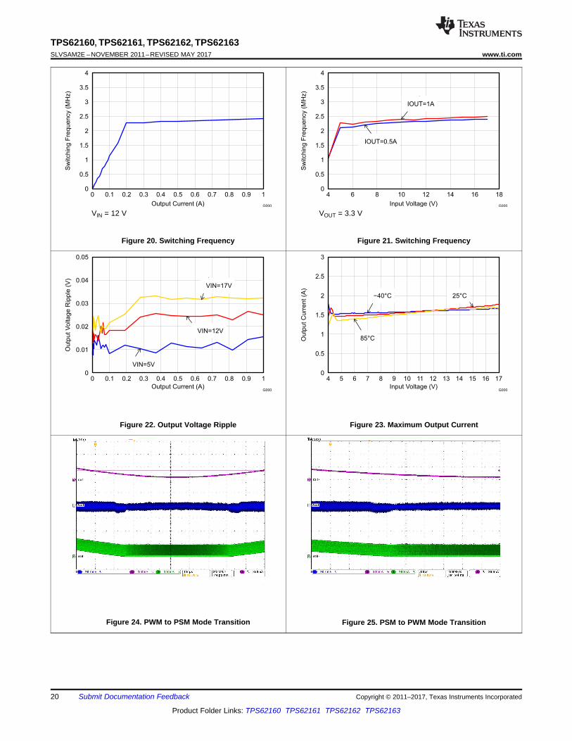
VIN = 12 V
Figure 20. Switching Frequency
VOUT = 3.3 V
Figure 21. Switching Frequency
Figure 22. Output Voltage Ripple Figure 23. Maximum Output Current
Figure 24. PWM to PSM Mode Transition Figure 25. PSM to PWM Mode Transition

21
TPS62160, TPS62161, TPS62162, TPS62163www.ti.com SLVSAM2E –NOVEMBER 2011–REVISED MAY 2017
Product Folder Links: TPS62160 TPS62161 TPS62162 TPS62163
Submit Documentation FeedbackCopyright © 2011–2017, Texas Instruments Incorporated
Figure 26. Load Transient Response in PWM Mode(500 mA to 1 A)
Figure 27. Load Transient Response from Power SaveMode (100 mA to 500 mA)
Figure 28. Load Transient Response in PWM Mode(500 mA to 1 A), Rising Edge
Figure 29. Load Transient Response in PWM Mode(500 mA to 1 A), Falling Edge
Figure 30. Startup with IOUT = 100 mA Figure 31. Startup with IOUT = 1 A

22
TPS62160, TPS62161, TPS62162, TPS62163SLVSAM2E –NOVEMBER 2011–REVISED MAY 2017 www.ti.com
Product Folder Links: TPS62160 TPS62161 TPS62162 TPS62163
Submit Documentation Feedback Copyright © 2011–2017, Texas Instruments Incorporated
IOUT = 66 mA
Figure 32. Typical Operation in Power Save Mode
IOUT = 1 A
Figure 33. Typical Operation in PWM Mode

22uF
1.8V / 1A
10uF
2.2µH
TPS62161
VIN
EN
AGND
PGND
SW
VOS
PG
FB
100k
(3 .. 17)V
22uF
2.5V / 1A
10uF
2.2µH(3 .. 17)V
TPS62160
390k
180k
VIN
EN
AGND
PGND
SW
VOS
PG
FB
100k
22uF
3.3V / 1A
10uF
2.2µH
TPS62162
VIN
EN
AGND
PGND
SW
VOS
PG
FB
100k
(3.3 .. 17)V
22uF
5V / 1A
10uF
2.2µH
TPS62163
VIN
EN
AGND
PGND
SW
VOS
PG
FB
100k
(5 .. 17)V
23
TPS62160, TPS62161, TPS62162, TPS62163www.ti.com SLVSAM2E –NOVEMBER 2011–REVISED MAY 2017
Product Folder Links: TPS62160 TPS62161 TPS62162 TPS62163
Submit Documentation FeedbackCopyright © 2011–2017, Texas Instruments Incorporated
9.3 System Examples
9.3.1 1-A Power SupplyThe following example circuits show various TPS6216x devices and input voltages that provide a 1-A powersupply with output voltage options.
space
space
Figure 34. 5 V / 1 A Power Supply
space
space
Figure 35. 3.3 V / 1 A Power Supply
space
space
Figure 36. 2.5 V / 1 A Power Supply
space
space
Figure 37. 1.8 V / 1 A Power Supply
22uF10uF
2.2µH(3 .. 17)V
TPS62160
51k
200k
VIN
EN
AGND
PGND
SW
VOS
PG
FB
100k
1V / 1A
22uF10uF
2.2µH(3 .. 17)V
TPS62160
75k
150k
VIN
EN
AGND
PGND
SW
VOS
PG
FB
100k
1.2V / 1A
22uF10uF
2.2µH(3 .. 17)V
TPS62160
130k
150k
VIN
EN
AGND
PGND
SW
VOS
PG
FB
100k
1.5V / 1A
24
TPS62160, TPS62161, TPS62162, TPS62163SLVSAM2E –NOVEMBER 2011–REVISED MAY 2017 www.ti.com
Product Folder Links: TPS62160 TPS62161 TPS62162 TPS62163
Submit Documentation Feedback Copyright © 2011–2017, Texas Instruments Incorporated
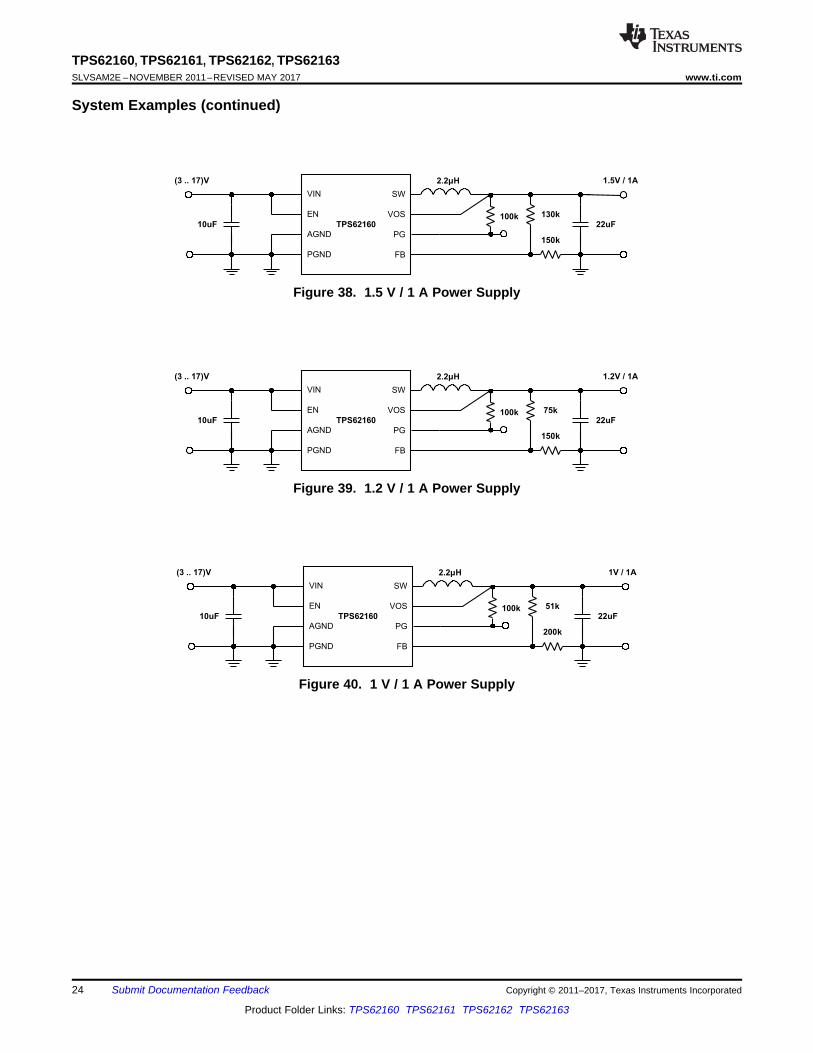
System Examples (continued)space
space
Figure 38. 1.5 V / 1 A Power Supply
space
space
Figure 39. 1.2 V / 1 A Power Supply
space
space
Figure 40. 1 V / 1 A Power Supply
22uF10uF
2.2µH(3 .. 12)V
TPS62160
680k
130k
VIN
EN
AGND
PGND
SW
VOS
PG
FB
100k
-5V
10uF
maxINOUTIN VVV £+
25
TPS62160, TPS62161, TPS62162, TPS62163www.ti.com SLVSAM2E –NOVEMBER 2011–REVISED MAY 2017
Product Folder Links: TPS62160 TPS62161 TPS62162 TPS62163
Submit Documentation FeedbackCopyright © 2011–2017, Texas Instruments Incorporated
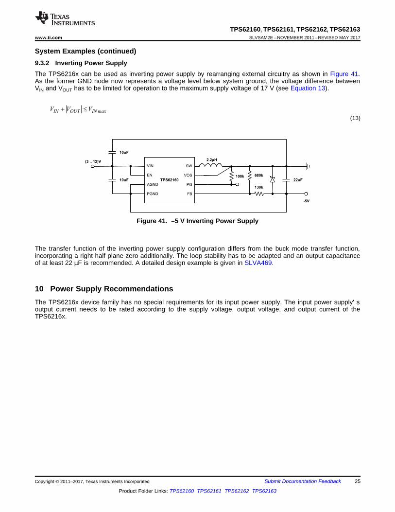
System Examples (continued)9.3.2 Inverting Power SupplyThe TPS6216x can be used as inverting power supply by rearranging external circuitry as shown in Figure 41.As the former GND node now represents a voltage level below system ground, the voltage difference betweenVIN and VOUT has to be limited for operation to the maximum supply voltage of 17 V (see Equation 13).
space
(13)
space
Figure 41. –5 V Inverting Power Supply
space
The transfer function of the inverting power supply configuration differs from the buck mode transfer function,incorporating a right half plane zero additionally. The loop stability has to be adapted and an output capacitanceof at least 22 µF is recommended. A detailed design example is given in SLVA469.
space
10 Power Supply RecommendationsThe TPS6216x device family has no special requirements for its input power supply. The input power supply' soutput current needs to be rated according to the supply voltage, output voltage, and output current of theTPS6216x.
VIN
GND VOUT
L1
R2 R1
C2
AGND
PG
VOS
C1
AGND
EN
VIN
PGND
SW
FB
26
TPS62160, TPS62161, TPS62162, TPS62163SLVSAM2E –NOVEMBER 2011–REVISED MAY 2017 www.ti.com
Product Folder Links: TPS62160 TPS62161 TPS62162 TPS62163
Submit Documentation Feedback Copyright © 2011–2017, Texas Instruments Incorporated
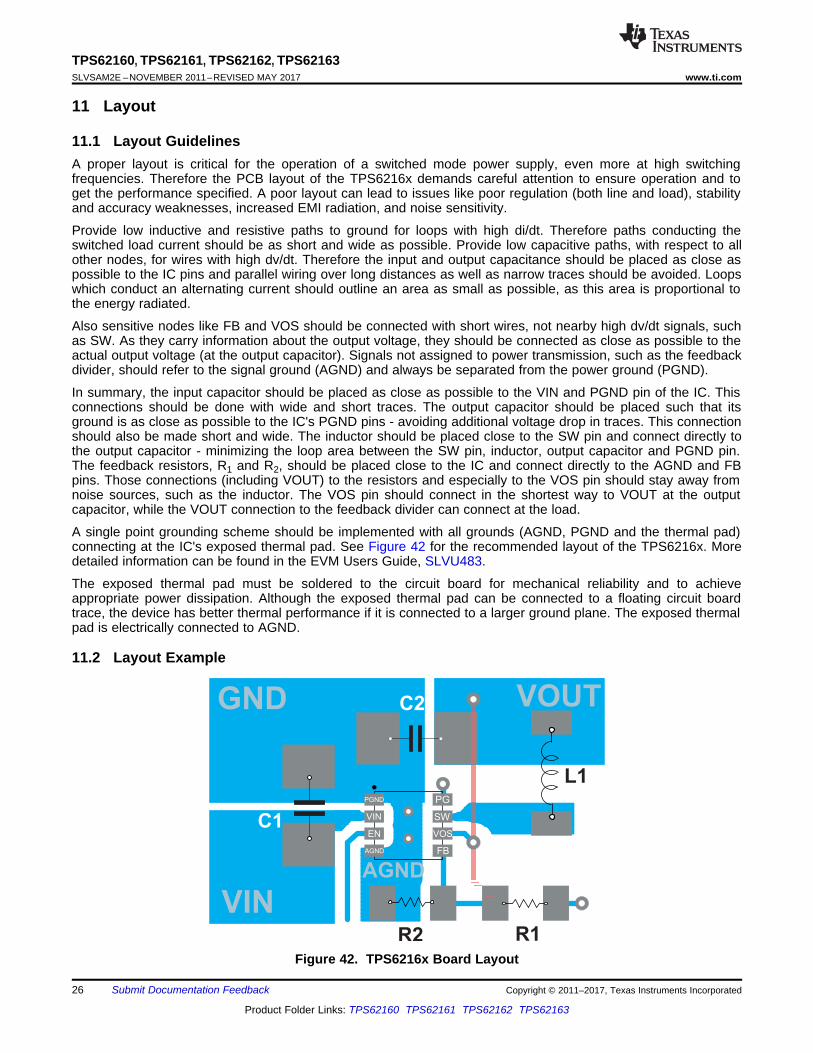
11 Layout
11.1 Layout GuidelinesA proper layout is critical for the operation of a switched mode power supply, even more at high switchingfrequencies. Therefore the PCB layout of the TPS6216x demands careful attention to ensure operation and toget the performance specified. A poor layout can lead to issues like poor regulation (both line and load), stabilityand accuracy weaknesses, increased EMI radiation, and noise sensitivity.
Provide low inductive and resistive paths to ground for loops with high di/dt. Therefore paths conducting theswitched load current should be as short and wide as possible. Provide low capacitive paths, with respect to allother nodes, for wires with high dv/dt. Therefore the input and output capacitance should be placed as close aspossible to the IC pins and parallel wiring over long distances as well as narrow traces should be avoided. Loopswhich conduct an alternating current should outline an area as small as possible, as this area is proportional tothe energy radiated.
Also sensitive nodes like FB and VOS should be connected with short wires, not nearby high dv/dt signals, suchas SW. As they carry information about the output voltage, they should be connected as close as possible to theactual output voltage (at the output capacitor). Signals not assigned to power transmission, such as the feedbackdivider, should refer to the signal ground (AGND) and always be separated from the power ground (PGND).
In summary, the input capacitor should be placed as close as possible to the VIN and PGND pin of the IC. Thisconnections should be done with wide and short traces. The output capacitor should be placed such that itsground is as close as possible to the IC's PGND pins - avoiding additional voltage drop in traces. This connectionshould also be made short and wide. The inductor should be placed close to the SW pin and connect directly tothe output capacitor - minimizing the loop area between the SW pin, inductor, output capacitor and PGND pin.The feedback resistors, R1 and R2, should be placed close to the IC and connect directly to the AGND and FBpins. Those connections (including VOUT) to the resistors and especially to the VOS pin should stay away fromnoise sources, such as the inductor. The VOS pin should connect in the shortest way to VOUT at the outputcapacitor, while the VOUT connection to the feedback divider can connect at the load.
A single point grounding scheme should be implemented with all grounds (AGND, PGND and the thermal pad)connecting at the IC's exposed thermal pad. See Figure 42 for the recommended layout of the TPS6216x. Moredetailed information can be found in the EVM Users Guide, SLVU483.
The exposed thermal pad must be soldered to the circuit board for mechanical reliability and to achieveappropriate power dissipation. Although the exposed thermal pad can be connected to a floating circuit boardtrace, the device has better thermal performance if it is connected to a larger ground plane. The exposed thermalpad is electrically connected to AGND.
11.2 Layout Example
Figure 42. TPS6216x Board Layout

27
TPS62160, TPS62161, TPS62162, TPS62163www.ti.com SLVSAM2E –NOVEMBER 2011–REVISED MAY 2017
Product Folder Links: TPS62160 TPS62161 TPS62162 TPS62163
Submit Documentation FeedbackCopyright © 2011–2017, Texas Instruments Incorporated
11.3 Thermal ConsiderationsImplementation of integrated circuits in low-profile and fine-pitch surface-mount packages typically requiresspecial attention to power dissipation. Many system-dependent issues such as thermal coupling, airflow, addedheat sinks and convection surfaces, and the presence of other heat-generating components affect the power-dissipation limits of a given component.
Three basic approaches for enhancing thermal performance are listed below:• Improving the power dissipation capability of the PCB design• Improving the thermal coupling of the component to the PCB by soldering the exposed thermal pad• Introducing airflow in the system
For more details on how to use the thermal parameters, see the application reports Thermal Characteristics ofLinear and Logic Packages Using JEDEC PCB Designs, SZZA017 and Semiconductor and IC Package ThermalMetrics, SPRA953.
The TPS6216x is designed for a maximum operating junction temperature (TJ) of 125°C. Therefore the maximumoutput power is limited by the power losses that can be dissipated over the actual thermal resistance, given bythe package and the surrounding PCB structures. If the thermal resistance of the package is given, the size ofthe surrounding copper area and a proper thermal connection of the IC can reduce the thermal resistance. Toget an improved thermal behavior, TI recommends to use top layer metal to connect the device with wide andthick metal lines. Internal ground layers can connect to vias directly under the IC for improved thermalperformance.
If short circuit or overload conditions are present, the device is protected by limiting internal power dissipation.

28
TPS62160, TPS62161, TPS62162, TPS62163SLVSAM2E –NOVEMBER 2011–REVISED MAY 2017 www.ti.com
Product Folder Links: TPS62160 TPS62161 TPS62162 TPS62163
Submit Documentation Feedback Copyright © 2011–2017, Texas Instruments Incorporated
12 Device and Documentation Support
12.1 Custom Design With WEBENCH® ToolsClick here to create a custom design using the TPS62160 device with the WEBENCH® Power Designer.1. Start by entering the input voltage (VIN), output voltage (VOUT), and output current (IOUT) requirements.2. Optimize the design for key parameters such as efficiency, footprint, and cost using the optimizer dial.3. Compare the generated design with other possible solutions from Texas Instruments.
The WEBENCH Power Designer provides a customized schematic along with a list of materials with real-timepricing and component availability.
In most cases, these actions are available:• Run electrical simulations to see important waveforms and circuit performance• Run thermal simulations to understand board thermal performance• Export customized schematic and layout into popular CAD formats• Print PDF reports for the design, and share the design with colleagues
Get more information about WEBENCH tools at www.ti.com/WEBENCH.
12.2 Device Support
12.2.1 Third-Party Products DisclaimerTI'S PUBLICATION OF INFORMATION REGARDING THIRD-PARTY PRODUCTS OR SERVICES DOES NOTCONSTITUTE AN ENDORSEMENT REGARDING THE SUITABILITY OF SUCH PRODUCTS OR SERVICESOR A WARRANTY, REPRESENTATION OR ENDORSEMENT OF SUCH PRODUCTS OR SERVICES, EITHERALONE OR IN COMBINATION WITH ANY TI PRODUCT OR SERVICE.
12.3 Documentation Support
12.3.1 Related DocumentationFor related documentation see the following:• Optimizing the TPS62130/40/50/60/70 Output Filter, SLVA463• Optimizing Transient Response of Internally Compensated dc-dc Converters With Feedforward Capacitor,
SLVA289• Using a Feedforward Capacitor to Improve Stability and Bandwidth of TPS62130/40/50/60/70, SLVA466• Thermal Characteristics of Linear and Logic Packages Using JEDEC PCB Designs, SZZA017
12.4 Related LinksThe table below lists quick access links. Categories include technical documents, support and communityresources, tools and software, and quick access to sample or buy.
Table 5. Related Links
PARTS PRODUCT FOLDER SAMPLE & BUY TECHNICALDOCUMENTS
TOOLS &SOFTWARE
SUPPORT &COMMUNITY
TPS62160 Click here Click here Click here Click here Click hereTPS62161 Click here Click here Click here Click here Click hereTPS62162 Click here Click here Click here Click here Click hereTPS62163 Click here Click here Click here Click here Click here
12.5 Community ResourcesThe following links connect to TI community resources. Linked contents are provided "AS IS" by the respectivecontributors. They do not constitute TI specifications and do not necessarily reflect TI's views; see TI's Terms ofUse.
29
TPS62160, TPS62161, TPS62162, TPS62163www.ti.com SLVSAM2E –NOVEMBER 2011–REVISED MAY 2017
Product Folder Links: TPS62160 TPS62161 TPS62162 TPS62163
Submit Documentation FeedbackCopyright © 2011–2017, Texas Instruments Incorporated
Community Resources (continued)TI E2E™ Online Community TI's Engineer-to-Engineer (E2E) Community. Created to foster collaboration
among engineers. At e2e.ti.com, you can ask questions, share knowledge, explore ideas and helpsolve problems with fellow engineers.
Design Support TI's Design Support Quickly find helpful E2E forums along with design support tools andcontact information for technical support.
12.6 TrademarksDCS-Control, E2E are trademarks of Texas Instruments.WEBENCH is a registered trademark of Texas Instruments.All other trademarks are the property of their respective owners.
12.7 Electrostatic Discharge CautionThese devices have limited built-in ESD protection. The leads should be shorted together or the device placed in conductive foamduring storage or handling to prevent electrostatic damage to the MOS gates.
12.8 GlossarySLYZ022 — TI Glossary.
This glossary lists and explains terms, acronyms, and definitions.
13 Mechanical, Packaging, and Orderable InformationThe following pages include mechanical, packaging, and orderable information. This information is the mostcurrent data available for the designated devices. This data is subject to change without notice and revision ofthis document. For browser-based versions of this data sheet, refer to the left-hand navigation.

PACKAGE OPTION ADDENDUM
www.ti.com 30-May-2017
Addendum-Page 1
PACKAGING INFORMATION
Orderable Device Status(1)
Package Type PackageDrawing
Pins PackageQty
Eco Plan(2)
Lead/Ball Finish(6)
MSL Peak Temp(3)
Op Temp (°C) Device Marking(4/5)
Samples
TPS62160DGKR ACTIVE VSSOP DGK 8 2500 Green (RoHS& no Sb/Br)
CU NIPDAUAG Level-1-260C-UNLIM -40 to 125 62160
TPS62160DGKT ACTIVE VSSOP DGK 8 250 Green (RoHS& no Sb/Br)
CU NIPDAUAG Level-1-260C-UNLIM -40 to 125 62160
TPS62160DSGR ACTIVE WSON DSG 8 3000 Green (RoHS& no Sb/Br)
CU NIPDAU Level-2-260C-1 YEAR -40 to 125 QTV
TPS62160DSGT ACTIVE WSON DSG 8 250 Green (RoHS& no Sb/Br)
CU NIPDAU Level-2-260C-1 YEAR -40 to 125 QTV
TPS62161DSGR ACTIVE WSON DSG 8 3000 Green (RoHS& no Sb/Br)
CU NIPDAU Level-2-260C-1 YEAR -40 to 125 QUB
TPS62161DSGT ACTIVE WSON DSG 8 250 Green (RoHS& no Sb/Br)
CU NIPDAU Level-2-260C-1 YEAR -40 to 125 QUB
TPS62162DSGR ACTIVE WSON DSG 8 3000 Green (RoHS& no Sb/Br)
CU NIPDAU Level-2-260C-1 YEAR -40 to 125 QUC
TPS62162DSGT ACTIVE WSON DSG 8 250 Green (RoHS& no Sb/Br)
CU NIPDAU Level-2-260C-1 YEAR -40 to 125 QUC
TPS62163DSGR ACTIVE WSON DSG 8 3000 Green (RoHS& no Sb/Br)
CU NIPDAU Level-2-260C-1 YEAR -40 to 125 QUD
TPS62163DSGT ACTIVE WSON DSG 8 250 Green (RoHS& no Sb/Br)
CU NIPDAU Level-2-260C-1 YEAR -40 to 125 QUD
(1) The marketing status values are defined as follows:ACTIVE: Product device recommended for new designs.LIFEBUY: TI has announced that the device will be discontinued, and a lifetime-buy period is in effect.NRND: Not recommended for new designs. Device is in production to support existing customers, but TI does not recommend using this part in a new design.PREVIEW: Device has been announced but is not in production. Samples may or may not be available.OBSOLETE: TI has discontinued the production of the device.
(2) RoHS: TI defines "RoHS" to mean semiconductor products that are compliant with the current EU RoHS requirements for all 10 RoHS substances, including the requirement that RoHS substancedo not exceed 0.1% by weight in homogeneous materials. Where designed to be soldered at high temperatures, "RoHS" products are suitable for use in specified lead-free processes. TI mayreference these types of products as "Pb-Free".RoHS Exempt: TI defines "RoHS Exempt" to mean products that contain lead but are compliant with EU RoHS pursuant to a specific EU RoHS exemption.Green: TI defines "Green" to mean the content of Chlorine (Cl) and Bromine (Br) based flame retardants meet JS709B low halogen requirements of <=1000ppm threshold. Antimony trioxide basedflame retardants must also meet the <=1000ppm threshold requirement.
(3) MSL, Peak Temp. - The Moisture Sensitivity Level rating according to the JEDEC industry standard classifications, and peak solder temperature.
PACKAGE OPTION ADDENDUM
www.ti.com 30-May-2017
Addendum-Page 2
(4) There may be additional marking, which relates to the logo, the lot trace code information, or the environmental category on the device.
(5) Multiple Device Markings will be inside parentheses. Only one Device Marking contained in parentheses and separated by a "~" will appear on a device. If a line is indented then it is a continuationof the previous line and the two combined represent the entire Device Marking for that device.
(6) Lead/Ball Finish - Orderable Devices may have multiple material finish options. Finish options are separated by a vertical ruled line. Lead/Ball Finish values may wrap to two lines if the finishvalue exceeds the maximum column width.
Important Information and Disclaimer:The information provided on this page represents TI's knowledge and belief as of the date that it is provided. TI bases its knowledge and belief on informationprovided by third parties, and makes no representation or warranty as to the accuracy of such information. Efforts are underway to better integrate information from third parties. TI has taken andcontinues to take reasonable steps to provide representative and accurate information but may not have conducted destructive testing or chemical analysis on incoming materials and chemicals.TI and TI suppliers consider certain information to be proprietary, and thus CAS numbers and other limited information may not be available for release.
In no event shall TI's liability arising out of such information exceed the total purchase price of the TI part(s) at issue in this document sold by TI to Customer on an annual basis.
OTHER QUALIFIED VERSIONS OF TPS62160, TPS62162 :
• Automotive: TPS62160-Q1, TPS62162-Q1
NOTE: Qualified Version Definitions:
• Automotive - Q100 devices qualified for high-reliability automotive applications targeting zero defects

TAPE AND REEL INFORMATION
*All dimensions are nominal
Device PackageType
PackageDrawing
Pins SPQ ReelDiameter
(mm)
ReelWidth
W1 (mm)
A0(mm)
B0(mm)
K0(mm)
P1(mm)
W(mm)
Pin1Quadrant
TPS62160DGKR VSSOP DGK 8 2500 330.0 12.4 5.3 3.4 1.4 8.0 12.0 Q1
TPS62160DGKT VSSOP DGK 8 250 180.0 12.4 5.3 3.4 1.4 8.0 12.0 Q1
TPS62160DSGR WSON DSG 8 3000 178.0 8.4 2.25 2.25 1.0 4.0 8.0 Q2
TPS62160DSGT WSON DSG 8 250 178.0 8.4 2.25 2.25 1.0 4.0 8.0 Q2
TPS62161DSGR WSON DSG 8 3000 180.0 8.4 2.3 2.3 1.15 4.0 8.0 Q2
TPS62161DSGT WSON DSG 8 250 180.0 8.4 2.3 2.3 1.15 4.0 8.0 Q2
TPS62162DSGR WSON DSG 8 3000 180.0 8.4 2.3 2.3 1.15 4.0 8.0 Q2
TPS62162DSGT WSON DSG 8 250 180.0 8.4 2.3 2.3 1.15 4.0 8.0 Q2
TPS62163DSGR WSON DSG 8 3000 180.0 8.4 2.3 2.3 1.15 4.0 8.0 Q2
TPS62163DSGT WSON DSG 8 250 180.0 8.4 2.3 2.3 1.15 4.0 8.0 Q2
PACKAGE MATERIALS INFORMATION
www.ti.com 23-Nov-2017
Pack Materials-Page 1
*All dimensions are nominal
Device Package Type Package Drawing Pins SPQ Length (mm) Width (mm) Height (mm)
TPS62160DGKR VSSOP DGK 8 2500 367.0 367.0 35.0
TPS62160DGKT VSSOP DGK 8 250 210.0 185.0 35.0
TPS62160DSGR WSON DSG 8 3000 205.0 200.0 33.0
TPS62160DSGT WSON DSG 8 250 205.0 200.0 33.0
TPS62161DSGR WSON DSG 8 3000 210.0 185.0 35.0
TPS62161DSGT WSON DSG 8 250 210.0 185.0 35.0
TPS62162DSGR WSON DSG 8 3000 210.0 185.0 35.0
TPS62162DSGT WSON DSG 8 250 210.0 185.0 35.0
TPS62163DSGR WSON DSG 8 3000 210.0 185.0 35.0
TPS62163DSGT WSON DSG 8 250 210.0 185.0 35.0
PACKAGE MATERIALS INFORMATION
www.ti.com 23-Nov-2017
Pack Materials-Page 2


www.ti.com
PACKAGE OUTLINE
C
SEE OPTIONALTERMINAL 8X 0.3
0.2
1.6 0.12X1.5
0.9 0.1
6X 0.5
8X 0.40.2
0.050.00
0.8 MAX
A 2.11.9
B
2.11.9
0.30.2
0.40.2
(0.2) TYP
WSON - 0.8 mm max heightDSG0008APLASTIC SMALL OUTLINE - NO LEAD
4218900/B 09/2017
PIN 1 INDEX AREA
SEATING PLANE
0.08 C
1
4 5
8
PIN 1 ID0.1 C A B0.05 C
THERMAL PADEXPOSED
9
NOTES: 1. All linear dimensions are in millimeters. Any dimensions in parenthesis are for reference only. Dimensioning and tolerancing per ASME Y14.5M. 2. This drawing is subject to change without notice. 3. The package thermal pad must be soldered to the printed circuit board for thermal and mechanical performance.
SCALE 5.500
OPTIONAL TERMINALTYPICAL

www.ti.com
EXAMPLE BOARD LAYOUT
0.07 MINALL AROUND
0.07 MAXALL AROUND
8X (0.25)
(1.6)
(1.9)
6X (0.5)
(0.9) ( 0.2) VIATYP
(0.55)
8X (0.5)
(R0.05) TYP
WSON - 0.8 mm max heightDSG0008APLASTIC SMALL OUTLINE - NO LEAD
4218900/B 09/2017
SYMM
1
45
8
LAND PATTERN EXAMPLESCALE:20X
SYMM 9
NOTES: (continued) 4. This package is designed to be soldered to a thermal pad on the board. For more information, see Texas Instruments literature number SLUA271 (www.ti.com/lit/slua271).5. Vias are optional depending on application, refer to device data sheet. If any vias are implemented, refer to their locations shown on this view. It is recommended that vias under paste be filled, plugged or tented.
SOLDER MASKOPENINGSOLDER MASK
METAL UNDER
SOLDER MASKDEFINED
METALSOLDER MASKOPENING
SOLDER MASK DETAILS
NON SOLDER MASKDEFINED
(PREFERRED)

www.ti.com
EXAMPLE STENCIL DESIGN
(R0.05) TYP
8X (0.25)
8X (0.5)
(0.9)
(0.7)
(1.9)
(0.45)
6X (0.5)
WSON - 0.8 mm max heightDSG0008APLASTIC SMALL OUTLINE - NO LEAD
4218900/B 09/2017
NOTES: (continued) 6. Laser cutting apertures with trapezoidal walls and rounded corners may offer better paste release. IPC-7525 may have alternate design recommendations.
SOLDER PASTE EXAMPLEBASED ON 0.125 mm THICK STENCIL
EXPOSED PAD 9:
87% PRINTED SOLDER COVERAGE BY AREA UNDER PACKAGESCALE:25X
SYMM
1
45
8
METAL
SYMM9


IMPORTANT NOTICE
Texas Instruments Incorporated (TI) reserves the right to make corrections, enhancements, improvements and other changes to itssemiconductor products and services per JESD46, latest issue, and to discontinue any product or service per JESD48, latest issue. Buyersshould obtain the latest relevant information before placing orders and should verify that such information is current and complete.TI’s published terms of sale for semiconductor products (http://www.ti.com/sc/docs/stdterms.htm) apply to the sale of packaged integratedcircuit products that TI has qualified and released to market. Additional terms may apply to the use or sale of other types of TI products andservices.Reproduction of significant portions of TI information in TI data sheets is permissible only if reproduction is without alteration and isaccompanied by all associated warranties, conditions, limitations, and notices. TI is not responsible or liable for such reproduceddocumentation. Information of third parties may be subject to additional restrictions. Resale of TI products or services with statementsdifferent from or beyond the parameters stated by TI for that product or service voids all express and any implied warranties for theassociated TI product or service and is an unfair and deceptive business practice. TI is not responsible or liable for any such statements.Buyers and others who are developing systems that incorporate TI products (collectively, “Designers”) understand and agree that Designersremain responsible for using their independent analysis, evaluation and judgment in designing their applications and that Designers havefull and exclusive responsibility to assure the safety of Designers' applications and compliance of their applications (and of all TI productsused in or for Designers’ applications) with all applicable regulations, laws and other applicable requirements. Designer represents that, withrespect to their applications, Designer has all the necessary expertise to create and implement safeguards that (1) anticipate dangerousconsequences of failures, (2) monitor failures and their consequences, and (3) lessen the likelihood of failures that might cause harm andtake appropriate actions. Designer agrees that prior to using or distributing any applications that include TI products, Designer willthoroughly test such applications and the functionality of such TI products as used in such applications.TI’s provision of technical, application or other design advice, quality characterization, reliability data or other services or information,including, but not limited to, reference designs and materials relating to evaluation modules, (collectively, “TI Resources”) are intended toassist designers who are developing applications that incorporate TI products; by downloading, accessing or using TI Resources in anyway, Designer (individually or, if Designer is acting on behalf of a company, Designer’s company) agrees to use any particular TI Resourcesolely for this purpose and subject to the terms of this Notice.TI’s provision of TI Resources does not expand or otherwise alter TI’s applicable published warranties or warranty disclaimers for TIproducts, and no additional obligations or liabilities arise from TI providing such TI Resources. TI reserves the right to make corrections,enhancements, improvements and other changes to its TI Resources. TI has not conducted any testing other than that specificallydescribed in the published documentation for a particular TI Resource.Designer is authorized to use, copy and modify any individual TI Resource only in connection with the development of applications thatinclude the TI product(s) identified in such TI Resource. NO OTHER LICENSE, EXPRESS OR IMPLIED, BY ESTOPPEL OR OTHERWISETO ANY OTHER TI INTELLECTUAL PROPERTY RIGHT, AND NO LICENSE TO ANY TECHNOLOGY OR INTELLECTUAL PROPERTYRIGHT OF TI OR ANY THIRD PARTY IS GRANTED HEREIN, including but not limited to any patent right, copyright, mask work right, orother intellectual property right relating to any combination, machine, or process in which TI products or services are used. Informationregarding or referencing third-party products or services does not constitute a license to use such products or services, or a warranty orendorsement thereof. Use of TI Resources may require a license from a third party under the patents or other intellectual property of thethird party, or a license from TI under the patents or other intellectual property of TI.TI RESOURCES ARE PROVIDED “AS IS” AND WITH ALL FAULTS. TI DISCLAIMS ALL OTHER WARRANTIES ORREPRESENTATIONS, EXPRESS OR IMPLIED, REGARDING RESOURCES OR USE THEREOF, INCLUDING BUT NOT LIMITED TOACCURACY OR COMPLETENESS, TITLE, ANY EPIDEMIC FAILURE WARRANTY AND ANY IMPLIED WARRANTIES OFMERCHANTABILITY, FITNESS FOR A PARTICULAR PURPOSE, AND NON-INFRINGEMENT OF ANY THIRD PARTY INTELLECTUALPROPERTY RIGHTS. TI SHALL NOT BE LIABLE FOR AND SHALL NOT DEFEND OR INDEMNIFY DESIGNER AGAINST ANY CLAIM,INCLUDING BUT NOT LIMITED TO ANY INFRINGEMENT CLAIM THAT RELATES TO OR IS BASED ON ANY COMBINATION OFPRODUCTS EVEN IF DESCRIBED IN TI RESOURCES OR OTHERWISE. IN NO EVENT SHALL TI BE LIABLE FOR ANY ACTUAL,DIRECT, SPECIAL, COLLATERAL, INDIRECT, PUNITIVE, INCIDENTAL, CONSEQUENTIAL OR EXEMPLARY DAMAGES INCONNECTION WITH OR ARISING OUT OF TI RESOURCES OR USE THEREOF, AND REGARDLESS OF WHETHER TI HAS BEENADVISED OF THE POSSIBILITY OF SUCH DAMAGES.Unless TI has explicitly designated an individual product as meeting the requirements of a particular industry standard (e.g., ISO/TS 16949and ISO 26262), TI is not responsible for any failure to meet such industry standard requirements.Where TI specifically promotes products as facilitating functional safety or as compliant with industry functional safety standards, suchproducts are intended to help enable customers to design and create their own applications that meet applicable functional safety standardsand requirements. Using products in an application does not by itself establish any safety features in the application. Designers mustensure compliance with safety-related requirements and standards applicable to their applications. Designer may not use any TI products inlife-critical medical equipment unless authorized officers of the parties have executed a special contract specifically governing such use.Life-critical medical equipment is medical equipment where failure of such equipment would cause serious bodily injury or death (e.g., lifesupport, pacemakers, defibrillators, heart pumps, neurostimulators, and implantables). Such equipment includes, without limitation, allmedical devices identified by the U.S. Food and Drug Administration as Class III devices and equivalent classifications outside the U.S.TI may expressly designate certain products as completing a particular qualification (e.g., Q100, Military Grade, or Enhanced Product).Designers agree that it has the necessary expertise to select the product with the appropriate qualification designation for their applicationsand that proper product selection is at Designers’ own risk. Designers are solely responsible for compliance with all legal and regulatoryrequirements in connection with such selection.Designer will fully indemnify TI and its representatives against any damages, costs, losses, and/or liabilities arising out of Designer’s non-compliance with the terms and provisions of this Notice.
Mailing Address: Texas Instruments, Post Office Box 655303, Dallas, Texas 75265Copyright © 2017, Texas Instruments Incorporated