
3-A Step-Down Regulator with Integrated Switcher datasheet ... · 16 pgnd 5 sw en 1 12 vdd 15 pgnd...
28
TPS53311 13 VIN 14 VIN 6 7 5 SW SW SW V IN 2.9 V to 6 V V IN V DD 2.9 V to 3.5 V Output All MLCCs 4 3 10 9 PGD C BST PGD FB COMP 12 11 2 VDD AGND SYNC 1 8 EN PS 15 PGND 16 PGND Pad VBST EN SYNC Copyright © 2016, Texas Instruments Incorporated Product Folder Sample & Buy Technical Documents Tools & Software Support & Community Reference Design An IMPORTANT NOTICE at the end of this data sheet addresses availability, warranty, changes, use in safety-critical applications, intellectual property matters and other important disclaimers. PRODUCTION DATA. TPS53311 SLUSA41B – JUNE 2010 – REVISED SEPTEMBER 2016 TPS53311 3-A Step-Down Regulator With Integrated Switcher 1 1 Features 1• 95.5% Maximum Efficiency • Continuous 3-A Output Current • Supports All MLCC Output Capacitor • SmoothPWM™ Auto-Skip Eco-mode™ for Light- Load Efficiency • Voltage Mode Control • Supports Master-Slave Interleaved Operation • Synchronization up to ±20% of Nominal Frequency • Conversion Voltage Range From 2.9 V to 6 V • Soft-Stop Output Discharge During Disable • Adjustable Output Voltage Ranging From 0.6 V to 0.84 V × V IN • Overcurrent, Overvoltage, and Overtemperature Protection • Small, 3 mm × 3 mm, 16-Pin VQFN Package • Open-Drain Power Good Indication • Internal Boot Strap Switch • Low R DS(on) , 24 mΩ With 3.3-V Input and 19-mΩ With 5-V Input • Supports Prebias Start-Up Functionality 2 Applications • 5-V Step-Down Rail • 3.3-V Step-Down Rail 3 Description The TPS53311 provides a fully integrated 3-V to 5-V V IN integrated synchronous FET converter solution with 16 total components, in 200 mm 2 of PCB area. Due to the low R DS(on) and TI Proprietary SmoothPWM™ skip mode of operation, it enables 95.5% peak efficiency, and over 90% efficiency at loads as light as 100 mA. It requires only two 22-μF ceramic output capacitors for a power-dense, 3-A solution. The TPS53311 features a 1.1-MHz switching frequency, SKIP mode operation support, prebias start-up, internal soft start, output soft discharge, internal VBST switch, power good, EN/input UVLO, overcurrent, overvoltage, undervoltage, and overtemperature protections and all ceramic output capacitor support. It supports supply voltage from 2.9 V to 3.5 V and conversion voltage from 2.9 V to 6 V, and output voltage is adjustable from 0.6 V to 0.84 V × V IN . The TPS53311 is available in the 3 mm × 3 mm 16-pin VQFN package (Green RoHs compliant and Pb free) and operates between –40°C and 85°C. Device Information (1) PART NUMBER PACKAGE BODY SIZE (NOM) TPS53311 VQFN (16) 3.00 mm × 3.00 mm (1) For all available packages, see the orderable addendum at the end of the data sheet. Typical Application Circuit
Transcript of 3-A Step-Down Regulator with Integrated Switcher datasheet ... · 16 pgnd 5 sw en 1 12 vdd 15 pgnd...

TPS53311
13
VIN
14
VIN
6 75
SW SW SW
VIN
2.9 V to 6 VVIN
VDD
2.9 V to 3.5 V
Output All MLCCs
4
3
10
9
PGD
CBST
PGD
FB
COMP
12
11
2
VDD
AGND
SYNC
1
8
EN
PS
15
PGND
16
PGND Pad
VBST
EN
SYNC
Copyright © 2016, Texas Instruments Incorporated
Product
Folder
Sample &Buy
Technical
Documents
Tools &
Software
Support &Community
ReferenceDesign
An IMPORTANT NOTICE at the end of this data sheet addresses availability, warranty, changes, use in safety-critical applications,intellectual property matters and other important disclaimers. PRODUCTION DATA.
TPS53311SLUSA41B –JUNE 2010–REVISED SEPTEMBER 2016
TPS53311 3-A Step-Down Regulator With Integrated Switcher
1
1 Features1• 95.5% Maximum Efficiency• Continuous 3-A Output Current• Supports All MLCC Output Capacitor• SmoothPWM™ Auto-Skip Eco-mode™ for Light-
Load Efficiency• Voltage Mode Control• Supports Master-Slave Interleaved Operation• Synchronization up to ±20% of Nominal
Frequency• Conversion Voltage Range From 2.9 V to 6 V• Soft-Stop Output Discharge During Disable• Adjustable Output Voltage Ranging From
0.6 V to 0.84 V × VIN
• Overcurrent, Overvoltage, and OvertemperatureProtection
• Small, 3 mm × 3 mm, 16-Pin VQFN Package• Open-Drain Power Good Indication• Internal Boot Strap Switch• Low RDS(on), 24 mΩ With 3.3-V Input and 19-mΩ
With 5-V Input• Supports Prebias Start-Up Functionality
2 Applications• 5-V Step-Down Rail• 3.3-V Step-Down Rail
3 DescriptionThe TPS53311 provides a fully integrated 3-V to 5-VVIN integrated synchronous FET converter solutionwith 16 total components, in 200 mm2 of PCB area.Due to the low RDS(on) and TI ProprietarySmoothPWM™ skip mode of operation, it enables95.5% peak efficiency, and over 90% efficiency atloads as light as 100 mA. It requires only two 22-µFceramic output capacitors for a power-dense, 3-Asolution.
The TPS53311 features a 1.1-MHz switchingfrequency, SKIP mode operation support, prebiasstart-up, internal soft start, output soft discharge,internal VBST switch, power good, EN/input UVLO,overcurrent, overvoltage, undervoltage, andovertemperature protections and all ceramic outputcapacitor support. It supports supply voltage from2.9 V to 3.5 V and conversion voltage from 2.9 V to6 V, and output voltage is adjustable from 0.6 V to0.84 V × VIN.
The TPS53311 is available in the 3 mm × 3 mm16-pin VQFN package (Green RoHs compliant andPb free) and operates between –40°C and 85°C.
Device Information(1)
PART NUMBER PACKAGE BODY SIZE (NOM)TPS53311 VQFN (16) 3.00 mm × 3.00 mm
(1) For all available packages, see the orderable addendum atthe end of the data sheet.
Typical Application Circuit

2
TPS53311SLUSA41B –JUNE 2010–REVISED SEPTEMBER 2016 www.ti.com
Product Folder Links: TPS53311
Submit Documentation Feedback Copyright © 2010–2016, Texas Instruments Incorporated
Table of Contents1 Features .................................................................. 12 Applications ........................................................... 13 Description ............................................................. 14 Revision History..................................................... 25 Pin Configuration and Functions ......................... 36 Specifications......................................................... 4
6.1 Absolute Maximum Ratings ...................................... 46.2 ESD Ratings.............................................................. 46.3 Recommended Operating Conditions....................... 46.4 Thermal Information .................................................. 56.5 Electrical Characteristics........................................... 56.6 Typical Characteristics .............................................. 7
7 Detailed Description .............................................. 97.1 Overview ................................................................... 97.2 Functional Block Diagram ......................................... 97.3 Feature Description................................................... 9
7.4 Device Functional Modes........................................ 118 Application and Implementation ........................ 13
8.1 Application Information............................................ 138.2 Typical Application .................................................. 13
9 Power Supply Recommendations ...................... 1910 Layout................................................................... 19
10.1 Layout Guidelines ................................................. 1910.2 Layout Example .................................................... 19
11 Device and Documentation Support ................. 2011.1 Documentation Support ........................................ 2011.2 Receiving Notification of Documentation Updates 2011.3 Community Resources.......................................... 2011.4 Trademarks ........................................................... 2011.5 Electrostatic Discharge Caution............................ 2011.6 Glossary ................................................................ 20
12 Mechanical, Packaging, and OrderableInformation ........................................................... 20
4 Revision HistoryNOTE: Page numbers for previous revisions may differ from page numbers in the current version.
Changes from Revision A (March 2011) to Revision B Page
• Added ESD Ratings table, Feature Description section, Device Functional Modes, Application and Implementationsection, Power Supply Recommendations section, Layout section, Device and Documentation Support section, andMechanical, Packaging, and Orderable Information section .................................................................................................. 1
• Deleted Ordering Information table; see POA at the end of the data sheet........................................................................... 1• Added Thermal Information table ........................................................................................................................................... 5• Deleted Package Dissipation Ratings table............................................................................................................................ 5• Changed value of component R2 in Typical Application Circuit Diagram From: 4.02 kΩ To: 2.67 kΩ ................................ 13• Changed value of component VOUT on TPS53311 Master in Master and Slave Configuration Schematic From: 1.2 V
To: 1.5 V ............................................................................................................................................................................... 17• Changed value of component R2 on TPS53311 Master in Master and Slave Configuration Schematic From: 4.02 kΩ
To: 2.67 kΩ ........................................................................................................................................................................... 17• Changed value of component VOUT on TPS53311 Slave in Master and Slave Configuration Schematic From: 1.5 V
To: 1.2 V ............................................................................................................................................................................... 17• Changed value of component R12 on TPS53311 Slave in Master and Slave Configuration Schematic From: 2.67 kΩ
To: 4.02 kΩ ........................................................................................................................................................................... 17
Changes from Original (June 2010) to Revision A Page
• Added bullets to Features....................................................................................................................................................... 1• Changed Description for clarity .............................................................................................................................................. 1• Changed Absolute Maximum Ratings output voltage (SW pin DC) minimum from 0.3 V to –1 V (typographical error) ....... 4• Added information regarding DE mode in Master/Slave Operation and Synchronization section ....................................... 11• Changed value of component C2 in Typical Application Circuit Diagram to 2.2 nF (typographical error) ........................... 13• Changed component labels and values in Master/Slave Configuration Schematic (typographical error) ........................... 17
16P
GN
D5
SW
1EN 12 VDD
15P
GN
D6
SW
2SYNC 11 AGND
14V
IN7
SW
3PGD 10 FB
13V
IN8
PS
4VBST 9 COMP
Not to scale
3
TPS53311www.ti.com SLUSA41B –JUNE 2010–REVISED SEPTEMBER 2016
Product Folder Links: TPS53311
Submit Documentation FeedbackCopyright © 2010–2016, Texas Instruments Incorporated
(1) B = Bidirectional, G = Ground, I = Input, O = Output, P = Supply
5 Pin Configuration and Functions
RGT Package16-Pin VQFN
Top View
Pin FunctionsPIN
TYPE (1) DESCRIPTIONNO. NAME1 EN I Enable. Internally pulled up to VDD with a 1.35-MΩ resistor.
2 SYNC B Synchronization signal for input interleaving. Master SYNC pin sends out 180° out-of-phase signal toslave SYNC. SYNC frequency must be within ±20% of slave nominal frequency.
3 PGD O Power good output flag. Open drain output. Pull up to an external rail through a resistor.4 VBST P Supply input for high-side MOSFET (bootstrap terminal). Connect capacitor from this pin to SW terminal.5 SW B Output inductor connection to integrated power devices.6 SW B Output inductor connection to integrated power devices.7 SW B Output inductor connection to integrated power devices.
8 PS I
Mode configuration pin (with 10 µA current):Connecting to ground: Forced CCM slave.Pulled high or floating (internal pulled high): Forced CCM master.Connect with 24.3 kΩ to GND: DE slave.Connect with 57.6 kΩ to GND: HEF mode.Connect with 105 kΩ to GND: reserved mode.Connect with 174 kΩ to GND: DE master.
9 COMP O Error amplifier compensation terminal. Type III compensation method is recommended for stability.10 FB I Voltage feedback. Also used for OVP, UVP, and PGD determination.11 AGND G Device analog ground terminal.12 VDD P Input bias supply for analog functions.13 VIN P Gate driver supply and power conversion voltage.14 VIN P Gate driver supply and power conversion voltage.15 PGND P IC power GND terminal.16 PGND P IC power GND terminal.

4
TPS53311SLUSA41B –JUNE 2010–REVISED SEPTEMBER 2016 www.ti.com
Product Folder Links: TPS53311
Submit Documentation Feedback Copyright © 2010–2016, Texas Instruments Incorporated
(1) Stresses beyond those listed under Absolute Maximum Ratings may cause permanent damage to the device. These are stress ratingsonly, which do not imply functional operation of the device at these or any other conditions beyond those indicated under RecommendedOperating Conditions. Exposure to absolute-maximum-rated conditions for extended periods may affect device reliability.
6 Specifications
6.1 Absolute Maximum Ratingsover operating free-air temperature range (unless otherwise noted) (1)
MIN MAX UNIT
Input voltage
VIN, EN –0.3 7
VVBST –0.3 17VBST(with respect to SW) –0.3 7FB, PS, VDD –0.3 3.7
Output voltage
SWDC –1 7
VPulse < 20 ns, E = 5 µJ –3 10
PGD –0.3 7COMP, SYNC –0.3 3.7PGND –0.3 0.3
Operating temperature, TA –40 85 °CJunction temperature, TJ –40 150 °CStorage temperature, Tstg –55 150 °C
(1) JEDEC document JEP155 states that 500-V HBM allows safe manufacturing with a standard ESD control process.(2) JEDEC document JEP157 states that 250-V CDM allows safe manufacturing with a standard ESD control process.
6.2 ESD RatingsVALUE UNIT
V(ESD) Electrostatic dischargeHuman-body model (HBM), per ANSI/ESDA/JEDEC JS-001 (1) ±2000
VCharged-device model (CDM), per JEDEC specification JESD22-C101 (2) ±500
6.3 Recommended Operating Conditionsover operating free-air temperature range (unless otherwise noted)
MIN NOM MAX UNIT
Input voltage
VIN 2.9 6
V
VDD 2.9 3.3 3.5VBST –0.1 13.5VBST(with respect to SW) –0.1 6EN –0.1 6FB, PS –0.1 3.5
Output voltage
SW –1 6.5
VPGD –0.1 6COMP, SYNC –0.1 3.5PGND –0.1 0.1
Junction temperature, TJ –40 125 °C

5
TPS53311www.ti.com SLUSA41B –JUNE 2010–REVISED SEPTEMBER 2016
Product Folder Links: TPS53311
Submit Documentation FeedbackCopyright © 2010–2016, Texas Instruments Incorporated
(1) For more information about traditional and new thermal metrics, see the Semiconductor and IC Package Thermal Metrics applicationreport.
6.4 Thermal Information
THERMAL METRIC (1)TPS53311
UNITRGT (VQFN)16 PINS
RθJA Junction-to-ambient thermal resistance 42.8 °C/WRθJC(top) Junction-to-case (top) thermal resistance 51.3 °C/WRθJB Junction-to-board thermal resistance 16 °C/WψJT Junction-to-top characterization parameter 0.7 °C/WψJB Junction-to-board characterization parameter 16 °C/WRθJC(bot) Junction-to-case (bottom) thermal resistance 4.4 °C/W
(1) Ensured by design. Not production tested.
6.5 Electrical Characteristicsover recommended free-air temperature range, VIN = 3.3 V, VVDD = 3.3 V, PGND = GND (unless otherwise noted)
PARAMETER TEST CONDITIONS MIN TYP MAX UNITSUPPLY: VOLTAGE, CURRENTS, AND UVLOVIN VIN supply voltage Nominal input voltage 2.9 6 VIVINSDN VIN shutdown current EN = LO 3 µAVUVLO VIN UVLO threshold Ramp up, EN = HI 2.8 VVUVLOHYS VIN UVLO hysteresis VIN UVLO Hysteresis 130 mVVDD Internal circuitry supply voltage Nominal 3.3-V input voltage 2.9 3.3 3.5 VIDDSDN VDD shut down current EN = LO 5 µAIDD Standby current EN = HI, no switching 2.2 3.5 mAVDDUVLO 3.3-V UVLO threshold Ramp up, EN = HI 2.8 VVDDUVLOHYS 3.3-V UVLO hysteresis 75 mVVOLTAGE FEEDBACK LOOP: VREF AND ERROR AMPLIFIERVVREF VREF Internal precision reference voltage 0.6 V
TOLVREF VREF Tolerance0°C ≤ TA ≤ 85°C –1% 1%–40°C ≤ TA ≤ 85°C –1.25% 1.25%
UGBW (1) Unity gain bandwidth 14 MHzAOL
(1) Open loop gain 80 dBIFBINT FB input leakage current Sourced from FB pin 30 nA
IEAMAX(1) Output sinking and sourcing
current CCOMP = 20 pF 5 mA
SR (1) Slew rate 5 V/µsOCP: OVER CURRENT AND ZERO CROSSING
IOCPL Overcurrent limit on upper FETWhen IOUT exceeds this threshold for 4consecutive cycles. VIN = 3.3 V,VOUT = 1.5 V with 1-µH inductor, TA = 25°C
4.2 4.5 4.8 A
IOCPHOne time overcurrent latch offon the lower FET
Immediately shut down when sensed currentreach this value. VIN = 3.3 V,VOUT = 1.5 V with 1-µH inductor, TA = 25°C
4.8 5.1 5.5 A
VZXOFF(1) Zero crossing comparator
internal offset PGND – SW, SKIP mode –4.5 –3 –1.5 mV
PROTECTION: OVP, UVP, PGD, AND INTERNAL THERMAL SHUTDOWN
VOVPOvervoltage protectionthreshold voltage Measured at FB wrt. VREF 114% 117% 120%
VUVPUndervoltage protectionthreshold voltage Measured at FB wrt. VREF 80% 83% 86%
VPGDL PGD low threshold Measured at FB wrt. VREF 80% 83% 86%

6
TPS53311SLUSA41B –JUNE 2010–REVISED SEPTEMBER 2016 www.ti.com
Product Folder Links: TPS53311
Submit Documentation Feedback Copyright © 2010–2016, Texas Instruments Incorporated
Electrical Characteristics (continued)over recommended free-air temperature range, VIN = 3.3 V, VVDD = 3.3 V, PGND = GND (unless otherwise noted)
PARAMETER TEST CONDITIONS MIN TYP MAX UNIT
(2) See PS pin description for levels.
VPGDU PGD upper threshold Measured at FB wrt. VREF 114% 117% 120%
VINMINPGMinimum VIN voltage for validPGD at start up.
Measured at VIN with 1-mA (or 2-mA) sinkcurrent on PGD pin at start up 1 V
THSD (1) Thermal shutdown Latch off controller, attempt soft-stop 130 140 150 °CTHSDHYS
(1) Thermal Shutdown hysteresis Controller restarts after temperature has dropped 40 °CLOGIC PINS: I/O VOLTAGE AND CURRENTVPGPD PGD pulldown voltage Pulldown voltage with 4-mA sink current 0.2 0.4 VIPGLK PGD leakage current Hi-Z leakage current, apply 3.3-V in off state –2 0 2 µARENPU Enable pullup resistor 1.35 MΩ
VENH EN logic high threshold 1.1 1.18 1.3 VVENHYS EN hysteresis 0.18 0.24 V
PSTHS PS mode threshold voltage
Level 1 to level 2 (2) 0.12
VLevel 2 to level 3 0.4Level 3 to level 4 0.8Level 4 to level 5 1.4Level 5 to level 6 2.2
IPS PS source 10-µA pullup current when enabled 8 10 12 µAfSYNCSL Slave SYNC frequency range Versus nominal switching frequency –20% 20%PWSYNC SYNC low pulse width 110 nsISYNC SYNC pin sink current 10 µAVSYNCTHS
(1) SYNC threshold Falling edge 1 VVSYNCHYS
(1) SYNC hysteresis 0.5 VBOOT STRAP: VOLTAGE AND LEAKAGE CURRENTIVBSTLK VBST leakage current VIN = 3.3 V, VVBST = 6.6 V, TA = 25°C 1 µATIMERS: SS, FREQUENCY, RAMP, ON TIME AND I/O TIMINGtSS_1 Delay after EN asserting EN = HI, master or HEF mode 0.2 mstSS_2 Delay after EN asserting EN = HI, slave waiting time 0.5 mstSS_3 Soft-start ramp-up time Rising from VSS = 0 V to VSS = 0.6 V 0.4 ms
tPGDENDLY PGD startup delay time Rising from VSS = 0 V to VSS = 0.6 V,from VSS reaching 0.6 V to VPGD going high 0.4 ms
tOVPDLYOvervoltage protection delaytime Time from FB out of 20% of VREF to OVP fault 1.0 1.7 2.5 µs
tUVPDLYUndervoltage protection delaytime Time from FB out of –20% of VREF to UVP fault 11 µs
fSW Switching frequency control Forced CCM mode 0.99 1.1 1.21 MHzRamp amplitude (1) 2.9 V < VIN < 6 V VIN/4 V
tMIN(off) Minimum OFF timeFCCM mode or DE mode 100 140
nsHEF mode 175 250
DMAX Maximum duty cycleFCCM mode and DE mode, fSW = 1.1 MHz,0°C ≤ TA ≤ 85°C 84% 89%
HEF mode, fSW = 1.1 MHz, 0°C ≤ TA ≤ 85°C 75% 81%
RSFTSTPSoft-discharge transistorresistance VEN = Low, VIN = 3.3 V, VOUT = 0.5 V 60 Ω

–40 –10 20 65 80 12535
TA
– Ambient Temperature – °C
0.590
0.580
0.585
0.620
0.610
0.615
0.605
0.595
0.600
VF
B–
Feed
back
Vo
ltag
e–
V
–25 5 50 95 110 0– 0.5
0.5 1.0 2.0 2.5 3.01.5
0.5
0.3
0.1
– 0.1
Output Current (A)
Ou
tpu
tV
olt
ag
eC
han
ge
(%)
VIN
= 5.0 V
VIN
= 3.3 V
– 0.3
0 0.5 1.0 2.0 2.5 3.01.5
IOUT
– Output Current – A
Skip Mode
VIN
= 5 V
84
80
82
96
92
94
90
86
88
h–
Eff
icie
ncy
–%
VOUT
= 2.5 V
VOUT
= 1.8 V
VOUT
= 1.5 V
VOUT
= 1.2 V
0 0.5 1.0 2.0 2.5 3.01.5
IOUT
– Output Current – A
84
80
82
96
92
94
90
86
88
h–
Eff
icie
ncy
–%
VOUT
= 2.5 V
VOUT
= 1.5 V
VOUT
= 1.2 V
VOUT
= 1.8 V
FCCM Mode
VIN
= 5 V
0
84
800.5 1.0 2.0 2.5 3.01.5
82
96
92
94
90
86
88
VOUT
= 2.5 V
VOUT
= 1.8 V
VOUT
= 1.5 V
VOUT
= 1.2 V
IOUT
– Output Current – A
h–
Eff
icie
ncy
–%
Skip Mode
VIN
= 3.3 V
VOUT
= 2.5 V
VOUT
= 1.8 V
VOUT
= 1.5 V
VOUT
= 1.2 V
FCCM Mode
VIN
= 3.3 V
0
84
800.5 1.0 2.0 2.5 3.01.5
82
96
92
94
90
86
88
IOUT
– Output Current – A
7
TPS53311www.ti.com SLUSA41B –JUNE 2010–REVISED SEPTEMBER 2016
Product Folder Links: TPS53311
Submit Documentation FeedbackCopyright © 2010–2016, Texas Instruments Incorporated
6.6 Typical CharacteristicsInductor IN06142 (1 µH, 5.4 mΩ) is used.
Figure 1. Efficiency vs Output Current,Skip Mode, VIN = 3.3 V
Figure 2. Efficiency vs Output Current,FCCM, VIN = 3.3 V
Figure 3. Efficiency vs Output Current,Skip Mode, VIN = 5 V
Figure 4. Efficiency vs Output Current,FCCM, VIN = 5 V
Figure 5. Feedback Voltage vs Ambient Temperature Figure 6. Output Voltage Change vs Output Current

HEF Mode
VIN
= 3.3 V
IOUT
= 0 A
EN (5 V/div)
VOUT
(1 V/div)
PGD (5 V/div)
t – Time – 4 ms/div
20
30
40
50
60
70
80
90
0.0 0.5 1.0 1.5 2.0 2.5 3.0
Output Current (A)
Tem
pera
ture
(C)
No Air Flow
VIN
= 5 V @
VOUT
= 0.6 V
VOUT
= 1.2 V
VOUT
= 1.8 V
VOUT
= 2.5 V
VOUT
= 3.3 V
VIN
= 3.3 V @
VOUT
= 0.6 V
VOUT
= 1.2 V
VOUT
= 1.8 V
VOUT
= 2.5 V
HEF Mode
VIN
= 3.3 V
IOUT
= 0 A
EN (5 V/div)
VOUT
(1 V/div)
PGD (5 V/div)
t – Time – 200 ms/div
HEF Mode
VIN
= 3.3 V
IOUT
= 0 A
EN (5 V/div)
VOUT
(1 V/div)
PGD (5 V/div)
t – Time – 200 ms/div
0.5 V pre-biased
0.0110
0.1 1.0 10
10 k
1000
100
Output Current (A)
Fre
qu
en
cy
(kH
z)
VIN
= 3.3 V
FCCM
HEF
DE
Mode
0.0110
0.1 1.0 10
10 k
1000
100
Output Current (A)
Fre
qu
en
cy
(kH
z)
VIN
= 5.0 V
FCCM
HEF
DE
Mode
8
TPS53311SLUSA41B –JUNE 2010–REVISED SEPTEMBER 2016 www.ti.com
Product Folder Links: TPS53311
Submit Documentation Feedback Copyright © 2010–2016, Texas Instruments Incorporated
Typical Characteristics (continued)Inductor IN06142 (1 µH, 5.4 mΩ) is used.
Figure 7. Frequency vs Output Currentat VIN = 3.3 V
Figure 8. Frequency vs Output Currentat VIN = 5 V
Figure 9. Normal Start-Up Waveform Figure 10. Prebias Start-Up Waveform
Figure 11. Soft-Stop Waveform Figure 12. Safe Operating Area
4
7
15
12
10
9
12
FB
COMP
SYNC
VBST
SW
PGND
VDD
TPS53311
EN
38
PS PGD
11
AGND
13
VIN
14
VIN
16 PGND
6 SW
UV/OV
Threshold
Generation
0.6 V +
+
+
+
0.6 V
SS
Enable
ControlOSC
Mode
Scanner
E/A
UV
OVControl
Logic
PWM
LL One-Shot
Overtemp
VOUT Discharge
0.6 V–17%
+PWM
Ramp
VIN UVLO
XCON
HDRV
LDRV
OCP Logic
VDD UVLO
0.6 V+17%5 SW
Copyright © 2016, Texas Instruments Incorporated
9
TPS53311www.ti.com SLUSA41B –JUNE 2010–REVISED SEPTEMBER 2016
Product Folder Links: TPS53311
Submit Documentation FeedbackCopyright © 2010–2016, Texas Instruments Incorporated
7 Detailed Description
7.1 OverviewThe TPS53311 is a high-efficiency switching regulator with two integrated N-channel MOSFETs and is capableof delivering up to 3 A of load current. The TPS53311 provides output voltage between 0.6 V and 0.84 × VIN from2.9-V to 6-V wide input voltage range.
This device employs five operation modes to fit various application requirements. The master and slave modeenables a two-phase interleaved operation to reduce input ripple. The skip mode operation provides reducedpower loss and increases the efficiency at light load. The unique, patented PWM modulator enables smooth lightload to heavy load transition while maintaining fast load transient.
7.2 Functional Block Diagram
7.3 Feature Description
7.3.1 Soft StartThe soft-start function reduces the inrush current during the start-up sequence. A slow-rising reference voltage isgenerated by the soft-start circuitry and sent to the input of the error amplifier. When the soft-start ramp voltageis less than 600 mV, the error amplifier uses this ramp voltage as the reference. When the ramp voltage reaches600 mV, the error amplifier switches to a fixed 600-mV reference. The typical soft-start time is 400 µs.

10
TPS53311SLUSA41B –JUNE 2010–REVISED SEPTEMBER 2016 www.ti.com
Product Folder Links: TPS53311
Submit Documentation Feedback Copyright © 2010–2016, Texas Instruments Incorporated
Feature Description (continued)7.3.2 Power GoodThe TPS53311 monitors the voltage on the FB pin. If the FB voltage is between 83% and 117% of the referencevoltage, the power good signal remains high. If the FB voltage falls outside of these limits, the internal open-drainoutput pulls the power good pin (PGD) low.
During start-up, the input voltage must be higher than 1 V to have valid power good logic, and the power goodsignal is delayed for 400 µs after the FB voltage falls to within the power good limits. There is also 10-µs delayduring the shutdown sequence.
7.3.3 Undervoltage Lockout (UVLO) FunctionThe TPS53311 provides undervoltage lockout (UVLO) protection for both power input (VIN) and bias input (VDD)voltage. If either of them is lower than the UVLO threshold voltage minus the hysteresis, the device shuts off.When the voltage rises above the threshold voltage, the device restarts. The typical UVLO rising threshold is2.8 V for both VIN and VVDD. A hysteresis voltage of 130 mV for VIN and 75 mV for VVDD is also provided toprevent glitch.
7.3.4 Overcurrent ProtectionThe TPS53311 continuously monitors the current flowing through the high-side and the low-side MOSFETs. Ifthe current through the high-side FET exceeds 4.5 A, the high-side FET turns off and the low-side FET turns onuntil the next PWM cycle. An overcurrent (OC) counter starts to increment each occurrence of an overcurrentevent. The converter shuts down immediately when the OC counter reaches four. The OC counter resets if thedetected current is less 4.5 A after an OC event.
Another set of overcurrent circuitry monitors the current flowing through low-side FET. If the current through thelow-side FET exceeds 5.1 A, the overcurrent protection is enabled and immediately turns off both the high-sideand the low-side FETs and shuts down the converter. The device is fully protected against overcurrent duringboth on-time and off-time. This protection is latched. See TPS53310 data sheet, 3-A Step-Down Regulator withIntegrated Switcher (SLUSA68), for information on hiccup overcurrent protection.
7.3.5 Overvoltage ProtectionThe TPS53311 monitors the voltage divided feedback voltage to detect overvoltage and undervoltage conditions.When the feedback voltage is greater than 117% of the reference, the high-side MOSFET turns off and the low-side MOSFET turns on. The output voltage then drops until it reaches the undervoltage threshold. At that pointthe low-side MOSFET turns off and the device enters a high-impedance state.
7.3.6 Undervoltage ProtectionWhen the feedback voltage is lower than 83% of the reference voltage, the undervoltage protection timer starts.If the feedback voltage remains lower than the undervoltage threshold voltage after 10 µs, the device turns offboth the high-side and the low-side MOSFETs and goes into a high-impedance state. This protection is latched.
7.3.7 Overtemperature ProtectionThe TPS53311 continuously monitors the die temperature. If the die temperature exceeds the threshold value(140°C typical), the device shuts off. When the device temperature falls to 40°C below the overtemperaturethreshold, it restarts and returns to normal operation.
7.3.8 Output DischargeWhen the enable pin is low, the TPS53311 discharges the output capacitors through an internal MOSFET switchbetween SW and PGND while high-side and low-side MOSFETs remain off. The typical discharge switch-onresistance is 60 Ω. This function is disabled when VIN is less than 1 V.

11
TPS53311www.ti.com SLUSA41B –JUNE 2010–REVISED SEPTEMBER 2016
Product Folder Links: TPS53311
Submit Documentation FeedbackCopyright © 2010–2016, Texas Instruments Incorporated
Feature Description (continued)7.3.9 Master and Slave Operation and SynchronizationTwo TPS53311 can operate interleaved when configured as master and slave. The SYNC pins of the twodevices are connected together for synchronization. In CCM, the master device sends the 180° out-of-phasepulse to the slave device through the SYNC pin, which determines the leading edge of the PWM pulse. If theslave device does not receive the SYNC pulse from the master device or if the SYNC connection is brokenduring operation, the slave device continues to operate using its own internal clock.
In DE mode, the master and slave switching node does not synchronize to each other if either one of them isoperating in DCM. When both master and slave enters CCM, the switching nodes of master and slavesynchronize to each other.
The SYNC pin of the slave device can also connect to external clock source within ±20% of the 1.1-MHzswitching frequency. The falling edge of the SYNC triggers the rising edge of the PWM signal.
7.4 Device Functional Modes
7.4.1 Operation ModeThe TPS53311 offers five operation modes determined by the PS pin connections listed in Table 1.
Table 1. Operation Mode Selection
PS PIN CONNECTION OPERATION MODE AUTO-SKIP AT LIGHT LOAD MASTER AND SLAVESUPPORT
GND FCCM Slave — Slave24.3 kΩ to GND DE Slave Yes Slave57.6 kΩ to GND HEF Mode Yes —174 kΩ to GND DE Master Yes Master
Floating or pulled to VDD FCCM Master — Master
In forced continuous conduction mode (FCCM), the high-side FET is ON during the on-time and the low-side FETis ON during the off-time. The switching is synchronized to the internal clock thus the switching frequency isfixed.
In diode emulation mode (DE), the high-side FET is ON during the on-time and low-side FET is ON during theoff-time until the inductor current reaches zero. An internal zero-crossing comparator detects the zero crossing ofinductor current from positive to negative. When the inductor current reaches zero, the comparator sends asignal to the logic control and turns off the low-side FET.
When the load is increased, the inductor current is always positive and the zero-crossing comparator does notsend a zero-crossing signal. The converter enters into continuous conduction mode (CCM) when no zero-crossing is detected for two consecutive PWM pulses. The switching synchronizes to the internal clock and theswitching frequency is fixed.
In high-efficiency mode (HEF), the operation is the same as diode emulation mode at light load. However, theconverter does not synchronize to the internal clock during CCM. Instead, the PWM modulator determines theswitching frequency.
7.4.2 Light Load OperationIn skip modes (DE and HEF) when the load current is less than one-half of the inductor peak current, theinductor current becomes negative by the end of off-time. During light load operation, the low-side MOSFET isturned off when the inductor current reaches zero. The energy delivered to the load per switching cycle isincreased compared to the normal PWM mode operation and the switching frequency is reduced. The switchingloss is reduced, thereby improving efficiency.
In both DE and HEF mode, the switching frequency is reduced in discontinuous conduction mode (DCM). Whenthe load current is 0 A, the minimum switching frequency is reached. The difference between VVBST and VSWmust be maintained at a value higher than 2.4 V.

12
TPS53311SLUSA41B –JUNE 2010–REVISED SEPTEMBER 2016 www.ti.com
Product Folder Links: TPS53311
Submit Documentation Feedback Copyright © 2010–2016, Texas Instruments Incorporated
7.4.3 Forced Continuous Conduction ModeWhen the PS pin is grounded or greater than 2.2 V, the TPS53311 is operating in forced continuous conductionmode in both light-load and heavy-load conditions. In this mode, the switching frequency remains constant overthe entire load range, making it suitable for applications that need tight control of switching frequency at a cost oflower efficiency at light load.

12
11
2
VDD
AGND
SYNC
TPS53311
1
8
EN
PS
4
3
VBST
PGD
10FB
L1
1 mH
9COMP
15
PGND
16
PGND
13
VIN
14
VIN
6 75
SW SW SW
EN
SYNC
C8
1 mF
R6
2.2 WC6
0.1 mF
VIN
C2 2.2 nF
R4
4.02 kW
C3
100 pF
C1
2.2 nF
R3
20 WPGD
R5
57.6 kW
C4
0.1 mFVIN
Output all MLCCs
C5
22 mF
COUT
3 x 22 mF
R1
4.02 kW
R2
2.67 kW
R7
20 kW
Copyright © 2016, Texas Instruments Incorporated
13
TPS53311www.ti.com SLUSA41B –JUNE 2010–REVISED SEPTEMBER 2016
Product Folder Links: TPS53311
Submit Documentation FeedbackCopyright © 2010–2016, Texas Instruments Incorporated
8 Application and Implementation
NOTEInformation in the following applications sections is not part of the TI componentspecification, and TI does not warrant its accuracy or completeness. TI’s customers areresponsible for determining suitability of components for their purposes. Customers shouldvalidate and test their design implementation to confirm system functionality.
8.1 Application InformationThe TPS53311 device is a high-efficiency synchronous-buck converter. The device suits low-output voltagepoint-of-load applications with 3-A or lower output current in computing and similar digital consumer applications.
8.2 Typical ApplicationThis design example describes a voltage-mode, 3-A synchronous buck converter with integrated MOSFETs. TheTPS53311 device provides a fixed 1.5-V output at up to 3 A from a 3.3-V input bus.
Figure 13. Typical 3.3-V Input Application Circuit Diagram
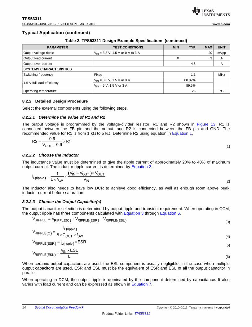
8.2.1 Design RequirementsTable 2 lists the parameters for this design example.
Table 2. TPS53311 Design Example SpecificationsPARAMETER TEST CONDITIONS MIN TYP MAX UNIT
INPUT CHARACTERISTICSInput voltage, VIN VIN 2.9 3.3 6 VMaximum input current VIN = 3.3 V, 1.5 V or 3 A 2.82 ANo load input current VIN = 3.3 V, 1.5 V or 0 A 40 mAOUTPUT CHARACTERISTICSOutput voltage, VO 1.485 1.5 1.515 V
Output voltage regulationLine regulation 0.1%Load regulation 1%
( )´
= IN
RIPPLE ESL
V ESLV
L
( ) ( )= ´RIPPLE ESR L rippleV I ESR
( )( )
=´ ´
L ripple
RIPPLE COUT SW
IV
8 C f
( ) ( ) ( )= + +RIPPLE RIPPLE C RIPPLE ESR RIPPLE ESLV V V V
( )( )- ´
= ´´ f
IN OUT OUTL ripple
SW IN
V V V1I
L V
OUT
0.6R2 R1
V 0.6= ´
-
14
TPS53311SLUSA41B –JUNE 2010–REVISED SEPTEMBER 2016 www.ti.com
Product Folder Links: TPS53311
Submit Documentation Feedback Copyright © 2010–2016, Texas Instruments Incorporated
Typical Application (continued)Table 2. TPS53311 Design Example Specifications (continued)
PARAMETER TEST CONDITIONS MIN TYP MAX UNITOutput voltage ripple VIN = 3.3 V, 1.5 V or 0 A to 3 A 20 mVppOutput load current 0 3 AOutput over current 4.5 ASYSTEMS CHARACTERISTICSSwitching frequency Fixed 1.1 MHz
1.5-V full load efficiencyVIN = 3.3 V, 1.5 V or 3 A 88.82%VIN = 5 V, 1.5 V or 3 A 89.5%
Operating temperature 25 °C
8.2.2 Detailed Design ProcedureSelect the external components using the following steps.
8.2.2.1 Determine the Value of R1 and R2The output voltage is programmed by the voltage-divider resistor, R1 and R2 shown in Figure 13. R1 isconnected between the FB pin and the output, and R2 is connected between the FB pin and GND. Therecommended value for R1 is from 1 kΩ to 5 kΩ. Determine R2 using equation in Equation 1.
(1)
8.2.2.2 Choose the InductorThe inductance value must be determined to give the ripple current of approximately 20% to 40% of maximumoutput current. The inductor ripple current is determined by Equation 2.
(2)
The inductor also needs to have low DCR to achieve good efficiency, as well as enough room above peakinductor current before saturation.
8.2.2.3 Choose the Output Capacitor(s)The output capacitor selection is determined by output ripple and transient requirement. When operating in CCM,the output ripple has three components calculated with Equation 3 through Equation 6.
(3)
(4)
(5)
(6)
When ceramic output capacitors are used, the ESL component is usually negligible. In the case when multipleoutput capacitors are used, ESR and ESL must be the equivalent of ESR and ESL of all the output capacitor inparallel.
When operating in DCM, the output ripple is dominated by the component determined by capacitance. It alsovaries with load current and can be expressed as shown in Equation 7.

( )´
=´
OUTIN ripple
SW IN
I DV
f C
=OUT
IN
VD
V
( ) ( )= ´ ´ -OUTIN rippleI I D 1 D
IL
VOUT
a x IL(ripple)
T1
VRIPPLE
a x T
IOUT
UDG-10055
( )
( )a =
ON DCM
ON CCM
t
t
( )( )( )
( )
a ´ -=
´ ´ ´
2
OUTL ripple
RIPPLE DCMOUT SW L ripple
I IV
2 C f I
15
TPS53311www.ti.com SLUSA41B –JUNE 2010–REVISED SEPTEMBER 2016
Product Folder Links: TPS53311
Submit Documentation FeedbackCopyright © 2010–2016, Texas Instruments Incorporated
where• α is the DCM on-time coefficient and can be expressed in Equation 8 (typical value 1.25) (7)
(8)
Figure 14. DCM VOUT Ripple Calculation
8.2.2.4 Choose the Input CapacitorThe selection of input capacitor must be determined by the ripple current requirement. The ripple currentgenerated by the converter needs to be absorbed by the input capacitors as well as the input source. The RMSripple current from the converter can be expressed in Equation 9.
where• D is the duty cycle and can be expressed as shown in Equation 10 (9)
(10)
To minimize the ripple current drawn from the input source, sufficient input decoupling capacitors must be placedclose to the device. TI recommends the ceramic capacitor because it provides low ESR and low ESL. The inputvoltage ripple can be calculated as shown in Equation 11 when the total input capacitance is determined.
(11)
8.2.2.5 Compensation DesignThe TPS53311 uses voltage mode control. To effectively compensate the power stage and ensure fast transientresponse, Type III compensation is typically used.
The control to output transfer function can be described in Equation 12.
= @´ p ´ ´æ ö´
´ p ´ ´ ç ÷+è ø
fP3
4 32 34
2 3
1 1
2 R CC C2 R
C C
=
´ p ´ ´
fP2
3 1
1
2 R C
=fP1 0
= @
´ p ´ + ´ ´ p ´ ´
fZ21 3 1 1 1
1 1
2 (R R ) C 2 R C
=
´ p ´ ´
fZ1
4 2
1
2 R C
( )( )
( ) ( )
+ ´ ´ + + ´ ´=
æ ö´´ ´ + ´ + ´ ´ ´ + ´ç ÷
+è ø
1 1 3 4 2EA
2 31 2 3 1 3 4
2 3
1 s C (R R ) 1 s R CG
C Cs R (C C ) 1 s C R 1 s R
C C
UDG-10057
Frequency
fZ1
fZ2
fP2
fP3
Gain
(dB
)R3
R1
C1
R2
R4 C2
C3
+COMP
VREF
UGD-10058
=
´ p ´ ´
fESR
OUT
1
2 ESR C
=
´ p ´ ´
fDP
OUT
1
2 L C
+ ´ ´= ´
æ ö+ ´ + ´ + + ´ ´ç ÷
+è ø
OUTCO
2OUT OUT
LOAD
1 s C ESRG 4
L1 s C (ESR DCR) s L C
DCR R
16
TPS53311SLUSA41B –JUNE 2010–REVISED SEPTEMBER 2016 www.ti.com
Product Folder Links: TPS53311
Submit Documentation Feedback Copyright © 2010–2016, Texas Instruments Incorporated
(12)
The output L-C filter introduces a double pole which can be calculated as shown in Equation 13.
(13)
The ESR zero can be calculated as shown in Equation 14.
(14)
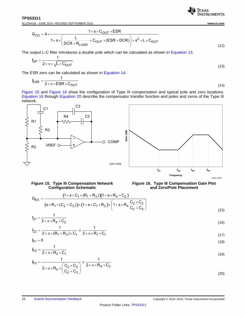
Figure 15 and Figure 16 show the configuration of Type III compensation and typical pole and zero locations.Equation 16 through Equation 20 describe the compensator transfer function and poles and zeros of the Type IIInetwork.
Figure 15. Type III Compensation NetworkConfiguration Schematic
Figure 16. Type III Compensation Gain Plotand Zero/Pole Placement
(15)
(16)
(17)
(18)
(19)
(20)

L1
12
11
2
VDD
AGND
SYNC
TPS53311
1
8
EN
PS
4
3
VBST
PGD
10FB
1 �H
9COMP
15
PGND
16
PGND
13
VIN
14
VIN
6 75
SW SW SW
EN _Master
C 81 �F
R 62.2 �
C 60.1 �F
VIN3.3 V
C2 2.2 nF R4
4.02 k �
C 3
100 pF
C12.2 nF
R320 �
PGD _Master
C40.1 �F VIN
Output all MLCCs
C 522 �F
C OUT3 x 22 �F
R1
4.02 k �
R22.67 k �
R720 k �
V OUT = 1.5 V
12
11
2
VDD
AGND
SYNC
TPS53311
1
8
EN
PS
4
3
VBST
PGD
10FB
L11
1 �H
9COMP
15
PGND
16
PGND
13
VIN
14
VIN
6 75
SW SW SW
EN _Slave
C 181 �F
R 162.2 �
C160.1 �F
C12 2.2 nF
R14
4.02 k �
C13 100 pF
C112.2 nFR13
20 �
PGD_Master
C140.1 �F VIN
Output all MLCCs
C 15
22 �F
C OUT3 x 22 �F
R 11
4.02 k �
R12
R1720 k �
VOUT =1.2VVIN
4.02 k �
Copyright © 2016, Texas Instruments Incorporated
17
TPS53311www.ti.com SLUSA41B –JUNE 2010–REVISED SEPTEMBER 2016
Product Folder Links: TPS53311
Submit Documentation FeedbackCopyright © 2010–2016, Texas Instruments Incorporated
The two zeros can be placed near the double pole frequency to cancel the response from the double pole. Onepole can be used to cancel ESR zero, and the other non-zero pole can be placed at half switching frequency toattenuate the high frequency noise and switching ripple. Suitable values can be selected to achieve acompromise between high phase margin and fast response. A phase margin higher than 45 degrees is requiredfor stable operation.
For DCM operation, a C3 between 56 pF and 150 pF is recommended for output capacitance between 20 µF to200 µF.
Figure 17 shows the master and slave configuration schematic for a design with a 3.3-V input.
Figure 17. Master and Slave Configuration Schematic

18
TPS53311SLUSA41B –JUNE 2010–REVISED SEPTEMBER 2016 www.ti.com
Product Folder Links: TPS53311
Submit Documentation Feedback Copyright © 2010–2016, Texas Instruments Incorporated
8.2.3 Application Curves
3.3 VIN, 1.5 V/3 AFigure 18. 1.5-V Output Ripple
3.3 VIN, 1.5 V/3 A and 1.2 V/3 AFigure 19. Master-Slave 180° Synchronization
5 VIN, 1.5 V/0 A-3 AFigure 20. 1.5-V Output Transient
3.3 VIN, 1.5 V/3 AFigure 21. 1.5-V Turnon Waveform
3.3 VIN, 1.5 V/3 AFigure 22. 1.5-V Turnoff Waveform

VIN
VIN
PGND
PGND
PS
SW
SW
SW
CO
MP
FB
AG
ND
VD
D
EN
SY
NC
PG
D
VB
ST
SW
GND Shape
GND Shape
VOUT
VIN Shape
GND Via
Etch under component
19
TPS53311www.ti.com SLUSA41B –JUNE 2010–REVISED SEPTEMBER 2016
Product Folder Links: TPS53311
Submit Documentation FeedbackCopyright © 2010–2016, Texas Instruments Incorporated
9 Power Supply RecommendationsThe TPS53311 device is designed to operate from an input voltage supply range from 2.9 V to 6 V (2.9 V to3.5 V biased). This input supply must be well regulated. Proper bypassing of input supplies and internalregulators is also critical for noise performance, as is PCB layout and grounding scheme. See therecommendations in Layout.
10 Layout
10.1 Layout GuidelinesGood layout is essential for stable power supply operation. Follow these guidelines for a clean PCB layout:• Separate the power ground and analog ground planes. Connect them together at one location.• Use four vias to connect the thermal pad to power ground.• Place VIN and VDD decoupling capacitors as close to the device as possible.• Use wide traces for VIN, VOUT, PGND and SW. These nodes carry high current and also serve as heat sinks.• Place feedback and compensation components as close to the device as possible.• Keep analog signals (FB, COMP) away from noisy signals (SW, SYNC, VBST).• See Using the TPS53311EVM-561, a 3-A Eco-mode™ Integrated Switcher With Master Slave (SLUU428) for
a layout example.
10.2 Layout Example
Figure 23. TPS533x Layout Example

20
TPS53311SLUSA41B –JUNE 2010–REVISED SEPTEMBER 2016 www.ti.com
Product Folder Links: TPS53311
Submit Documentation Feedback Copyright © 2010–2016, Texas Instruments Incorporated
11 Device and Documentation Support
11.1 Documentation Support
11.1.1 Related DocumentationFor related documentation see the following:• 3-A Step-Down Regulator with Integrated Switcher (SLUSA68)• Using the TPS53311EVM-561, a 3-A Eco-mode™ Integrated Switcher With Master Slave (SLUU428)
11.2 Receiving Notification of Documentation UpdatesTo receive notification of documentation updates, navigate to the device product folder on ti.com. In the upperright corner, click on Alert me to register and receive a weekly digest of any product information that haschanged. For change details, review the revision history included in any revised document.
11.3 Community ResourcesThe following links connect to TI community resources. Linked contents are provided "AS IS" by the respectivecontributors. They do not constitute TI specifications and do not necessarily reflect TI's views; see TI's Terms ofUse.
TI E2E™ Online Community TI's Engineer-to-Engineer (E2E) Community. Created to foster collaborationamong engineers. At e2e.ti.com, you can ask questions, share knowledge, explore ideas and helpsolve problems with fellow engineers.
Design Support TI's Design Support Quickly find helpful E2E forums along with design support tools andcontact information for technical support.
11.4 TrademarksSmoothPWM, Eco-mode, E2E are trademarks of Texas Instruments.All other trademarks are the property of their respective owners.
11.5 Electrostatic Discharge CautionThese devices have limited built-in ESD protection. The leads should be shorted together or the device placed in conductive foamduring storage or handling to prevent electrostatic damage to the MOS gates.
11.6 GlossarySLYZ022 — TI Glossary.
This glossary lists and explains terms, acronyms, and definitions.
12 Mechanical, Packaging, and Orderable InformationThe following pages include mechanical, packaging, and orderable information. This information is the mostcurrent data available for the designated devices. This data is subject to change without notice and revision ofthis document. For browser-based versions of this data sheet, refer to the left-hand navigation.

PACKAGE OPTION ADDENDUM
www.ti.com 11-Aug-2017
Addendum-Page 1
PACKAGING INFORMATION
Orderable Device Status(1)
Package Type PackageDrawing
Pins PackageQty
Eco Plan(2)
Lead/Ball Finish(6)
MSL Peak Temp(3)
Op Temp (°C) Device Marking(4/5)
Samples
TPS53311RGTR ACTIVE VQFN RGT 16 3000 Green (RoHS& no Sb/Br)
CU NIPDAU Level-2-260C-1 YEAR -40 to 85 3311
TPS53311RGTT ACTIVE VQFN RGT 16 250 Green (RoHS& no Sb/Br)
CU NIPDAU Level-2-260C-1 YEAR -40 to 85 3311
(1) The marketing status values are defined as follows:ACTIVE: Product device recommended for new designs.LIFEBUY: TI has announced that the device will be discontinued, and a lifetime-buy period is in effect.NRND: Not recommended for new designs. Device is in production to support existing customers, but TI does not recommend using this part in a new design.PREVIEW: Device has been announced but is not in production. Samples may or may not be available.OBSOLETE: TI has discontinued the production of the device.
(2) RoHS: TI defines "RoHS" to mean semiconductor products that are compliant with the current EU RoHS requirements for all 10 RoHS substances, including the requirement that RoHS substancedo not exceed 0.1% by weight in homogeneous materials. Where designed to be soldered at high temperatures, "RoHS" products are suitable for use in specified lead-free processes. TI mayreference these types of products as "Pb-Free".RoHS Exempt: TI defines "RoHS Exempt" to mean products that contain lead but are compliant with EU RoHS pursuant to a specific EU RoHS exemption.Green: TI defines "Green" to mean the content of Chlorine (Cl) and Bromine (Br) based flame retardants meet JS709B low halogen requirements of <=1000ppm threshold. Antimony trioxide basedflame retardants must also meet the <=1000ppm threshold requirement.
(3) MSL, Peak Temp. - The Moisture Sensitivity Level rating according to the JEDEC industry standard classifications, and peak solder temperature.
(4) There may be additional marking, which relates to the logo, the lot trace code information, or the environmental category on the device.
(5) Multiple Device Markings will be inside parentheses. Only one Device Marking contained in parentheses and separated by a "~" will appear on a device. If a line is indented then it is a continuationof the previous line and the two combined represent the entire Device Marking for that device.
(6) Lead/Ball Finish - Orderable Devices may have multiple material finish options. Finish options are separated by a vertical ruled line. Lead/Ball Finish values may wrap to two lines if the finishvalue exceeds the maximum column width.
Important Information and Disclaimer:The information provided on this page represents TI's knowledge and belief as of the date that it is provided. TI bases its knowledge and belief on informationprovided by third parties, and makes no representation or warranty as to the accuracy of such information. Efforts are underway to better integrate information from third parties. TI has taken andcontinues to take reasonable steps to provide representative and accurate information but may not have conducted destructive testing or chemical analysis on incoming materials and chemicals.TI and TI suppliers consider certain information to be proprietary, and thus CAS numbers and other limited information may not be available for release.
In no event shall TI's liability arising out of such information exceed the total purchase price of the TI part(s) at issue in this document sold by TI to Customer on an annual basis.

PACKAGE OPTION ADDENDUM
www.ti.com 11-Aug-2017
Addendum-Page 2

TAPE AND REEL INFORMATION
*All dimensions are nominal
Device PackageType
PackageDrawing
Pins SPQ ReelDiameter
(mm)
ReelWidth
W1 (mm)
A0(mm)
B0(mm)
K0(mm)
P1(mm)
W(mm)
Pin1Quadrant
TPS53311RGTR VQFN RGT 16 3000 330.0 12.4 3.3 3.3 1.1 8.0 12.0 Q2
TPS53311RGTR VQFN RGT 16 3000 330.0 12.4 3.3 3.3 1.1 8.0 12.0 Q2
TPS53311RGTT VQFN RGT 16 250 180.0 12.4 3.3 3.3 1.1 8.0 12.0 Q2
TPS53311RGTT VQFN RGT 16 250 180.0 12.5 3.3 3.3 1.1 8.0 12.0 Q2
PACKAGE MATERIALS INFORMATION
www.ti.com 11-Aug-2017
Pack Materials-Page 1

*All dimensions are nominal
Device Package Type Package Drawing Pins SPQ Length (mm) Width (mm) Height (mm)
TPS53311RGTR VQFN RGT 16 3000 367.0 367.0 35.0
TPS53311RGTR VQFN RGT 16 3000 338.0 355.0 50.0
TPS53311RGTT VQFN RGT 16 250 210.0 185.0 35.0
TPS53311RGTT VQFN RGT 16 250 338.0 355.0 50.0
PACKAGE MATERIALS INFORMATION
www.ti.com 11-Aug-2017
Pack Materials-Page 2


IMPORTANT NOTICE
Texas Instruments Incorporated (TI) reserves the right to make corrections, enhancements, improvements and other changes to itssemiconductor products and services per JESD46, latest issue, and to discontinue any product or service per JESD48, latest issue. Buyersshould obtain the latest relevant information before placing orders and should verify that such information is current and complete.TI’s published terms of sale for semiconductor products (http://www.ti.com/sc/docs/stdterms.htm) apply to the sale of packaged integratedcircuit products that TI has qualified and released to market. Additional terms may apply to the use or sale of other types of TI products andservices.Reproduction of significant portions of TI information in TI data sheets is permissible only if reproduction is without alteration and isaccompanied by all associated warranties, conditions, limitations, and notices. TI is not responsible or liable for such reproduceddocumentation. Information of third parties may be subject to additional restrictions. Resale of TI products or services with statementsdifferent from or beyond the parameters stated by TI for that product or service voids all express and any implied warranties for theassociated TI product or service and is an unfair and deceptive business practice. TI is not responsible or liable for any such statements.Buyers and others who are developing systems that incorporate TI products (collectively, “Designers”) understand and agree that Designersremain responsible for using their independent analysis, evaluation and judgment in designing their applications and that Designers havefull and exclusive responsibility to assure the safety of Designers' applications and compliance of their applications (and of all TI productsused in or for Designers’ applications) with all applicable regulations, laws and other applicable requirements. Designer represents that, withrespect to their applications, Designer has all the necessary expertise to create and implement safeguards that (1) anticipate dangerousconsequences of failures, (2) monitor failures and their consequences, and (3) lessen the likelihood of failures that might cause harm andtake appropriate actions. Designer agrees that prior to using or distributing any applications that include TI products, Designer willthoroughly test such applications and the functionality of such TI products as used in such applications.TI’s provision of technical, application or other design advice, quality characterization, reliability data or other services or information,including, but not limited to, reference designs and materials relating to evaluation modules, (collectively, “TI Resources”) are intended toassist designers who are developing applications that incorporate TI products; by downloading, accessing or using TI Resources in anyway, Designer (individually or, if Designer is acting on behalf of a company, Designer’s company) agrees to use any particular TI Resourcesolely for this purpose and subject to the terms of this Notice.TI’s provision of TI Resources does not expand or otherwise alter TI’s applicable published warranties or warranty disclaimers for TIproducts, and no additional obligations or liabilities arise from TI providing such TI Resources. TI reserves the right to make corrections,enhancements, improvements and other changes to its TI Resources. TI has not conducted any testing other than that specificallydescribed in the published documentation for a particular TI Resource.Designer is authorized to use, copy and modify any individual TI Resource only in connection with the development of applications thatinclude the TI product(s) identified in such TI Resource. NO OTHER LICENSE, EXPRESS OR IMPLIED, BY ESTOPPEL OR OTHERWISETO ANY OTHER TI INTELLECTUAL PROPERTY RIGHT, AND NO LICENSE TO ANY TECHNOLOGY OR INTELLECTUAL PROPERTYRIGHT OF TI OR ANY THIRD PARTY IS GRANTED HEREIN, including but not limited to any patent right, copyright, mask work right, orother intellectual property right relating to any combination, machine, or process in which TI products or services are used. Informationregarding or referencing third-party products or services does not constitute a license to use such products or services, or a warranty orendorsement thereof. Use of TI Resources may require a license from a third party under the patents or other intellectual property of thethird party, or a license from TI under the patents or other intellectual property of TI.TI RESOURCES ARE PROVIDED “AS IS” AND WITH ALL FAULTS. TI DISCLAIMS ALL OTHER WARRANTIES ORREPRESENTATIONS, EXPRESS OR IMPLIED, REGARDING RESOURCES OR USE THEREOF, INCLUDING BUT NOT LIMITED TOACCURACY OR COMPLETENESS, TITLE, ANY EPIDEMIC FAILURE WARRANTY AND ANY IMPLIED WARRANTIES OFMERCHANTABILITY, FITNESS FOR A PARTICULAR PURPOSE, AND NON-INFRINGEMENT OF ANY THIRD PARTY INTELLECTUALPROPERTY RIGHTS. TI SHALL NOT BE LIABLE FOR AND SHALL NOT DEFEND OR INDEMNIFY DESIGNER AGAINST ANY CLAIM,INCLUDING BUT NOT LIMITED TO ANY INFRINGEMENT CLAIM THAT RELATES TO OR IS BASED ON ANY COMBINATION OFPRODUCTS EVEN IF DESCRIBED IN TI RESOURCES OR OTHERWISE. IN NO EVENT SHALL TI BE LIABLE FOR ANY ACTUAL,DIRECT, SPECIAL, COLLATERAL, INDIRECT, PUNITIVE, INCIDENTAL, CONSEQUENTIAL OR EXEMPLARY DAMAGES INCONNECTION WITH OR ARISING OUT OF TI RESOURCES OR USE THEREOF, AND REGARDLESS OF WHETHER TI HAS BEENADVISED OF THE POSSIBILITY OF SUCH DAMAGES.Unless TI has explicitly designated an individual product as meeting the requirements of a particular industry standard (e.g., ISO/TS 16949and ISO 26262), TI is not responsible for any failure to meet such industry standard requirements.Where TI specifically promotes products as facilitating functional safety or as compliant with industry functional safety standards, suchproducts are intended to help enable customers to design and create their own applications that meet applicable functional safety standardsand requirements. Using products in an application does not by itself establish any safety features in the application. Designers mustensure compliance with safety-related requirements and standards applicable to their applications. Designer may not use any TI products inlife-critical medical equipment unless authorized officers of the parties have executed a special contract specifically governing such use.Life-critical medical equipment is medical equipment where failure of such equipment would cause serious bodily injury or death (e.g., lifesupport, pacemakers, defibrillators, heart pumps, neurostimulators, and implantables). Such equipment includes, without limitation, allmedical devices identified by the U.S. Food and Drug Administration as Class III devices and equivalent classifications outside the U.S.TI may expressly designate certain products as completing a particular qualification (e.g., Q100, Military Grade, or Enhanced Product).Designers agree that it has the necessary expertise to select the product with the appropriate qualification designation for their applicationsand that proper product selection is at Designers’ own risk. Designers are solely responsible for compliance with all legal and regulatoryrequirements in connection with such selection.Designer will fully indemnify TI and its representatives against any damages, costs, losses, and/or liabilities arising out of Designer’s non-compliance with the terms and provisions of this Notice.
Mailing Address: Texas Instruments, Post Office Box 655303, Dallas, Texas 75265Copyright © 2017, Texas Instruments Incorporated