LM43602 Datasheet - TI. · PDF filesw vin pgnd cboot vcc bias sync rt pgood en ss/trk fb sw...
49
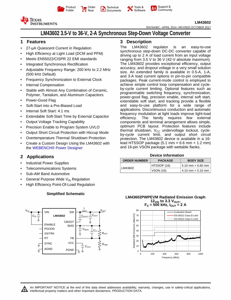
0 10 20 30 40 50 60 70 80 0 200 400 600 800 1000 Radiated EMI Emissions (dBμV/m) Frequency (MHz) Evaluation Board EN 55022 Class B Limit EN 55022 Class A Limit C001 C001 SW VIN PGND CBOOT VCC BIAS SYNC RT ENABLE SS/TRK AGND FB LM43602 V IN C OUT C BOOT C IN C VCC V OUT C BIAS R FBT R FBB C FF L PGOOD Product Folder Order Now Technical Documents Tools & Software Support & Community An IMPORTANT NOTICE at the end of this data sheet addresses availability, warranty, changes, use in safety-critical applications, intellectual property matters and other important disclaimers. PRODUCTION DATA. LM43602 SNVSA36C – APRIL 2014 – REVISED OCTOBER 2017 LM43602 3.5-V to 36-V, 2-A Synchronous Step-Down Voltage Converter 1 1 Features 1• 27-μA Quiescent Current in Regulation • High Efficiency at Light Load (DCM and PFM) • Meets EN55022/CISPR 22 EMI standards • Integrated Synchronous Rectification • Adjustable Frequency Range: 200 kHz to 2.2 MHz (500 kHz Default) • Frequency Synchronization to External Clock • Internal Compensation • Stable with Almost Any Combination of Ceramic, Polymer, Tantalum, and Aluminum Capacitors • Power-Good Flag • Soft-Start into a Pre-Biased Load • Internal Soft Start: 4.1 ms • Extendable Soft-Start Time by External Capacitor • Output Voltage Tracking Capability • Precision Enable to Program System UVLO • Output Short Circuit Protection with Hiccup Mode • Overtemperature Thermal Shutdown Protection • Create a Custom Design Using the LM43602 with the WEBENCH® Power Designer 2 Applications • Industrial Power Supplies • Telecommunications Systems • Sub-AM Band Automotive • General Purpose Wide V IN Regulation • High Efficiency Point-Of-Load Regulation space 3 Description The LM43602 regulator is an easy-to-use synchronous step-down DC-DC converter capable of driving up to 2 A of load current from an input voltage ranging from 3.5 V to 36 V (42-V absolute maximum). The LM43602 provides exceptional efficiency, output accuracy, and dropout voltage in a very small solution size. An extended family is available in 0.5-A, 1-A, and 3-A load current options in pin-to-pin compatible packages. Peak current-mode control is employed to achieve simple control loop compensation and cycle- by-cycle current limiting. Optional features such as programmable switching frequency, synchronization, power-good flag, precision enable, internal soft start, extendable soft start, and tracking provide a flexible and easy-to-use platform for a wide range of applications. Discontinuous conduction and automatic frequency modulation at light loads improve light-load efficiency. The family requires few external components and terminal arrangement allows simple, optimum PCB layout. Protection features include thermal shutdown, V CC undervoltage lockout, cycle- by-cycle current limit, and output short circuit protection. The LM43602 device is available in a 16- lead HTSSOP package (5.1 mm × 6.6 mm × 1.2 mm) and 16-pin VSON package with wettable flanks. Device Information ORDER NUMBER PACKAGE BODY SIZE LM43602 HTSSOP (16) 5.10 mm × 6.60 mm VSON (16) 4.10 mm × 5.10 mm Simplified Schematic LM43602PWPEVM Radiated Emission Graph 12 VIN to 3.3 V OUT , F S = 500 kHz, I OUT =2A
Transcript of LM43602 Datasheet - TI. · PDF filesw vin pgnd cboot vcc bias sync rt pgood en ss/trk fb sw...
0
10
20
30
40
50
60
70
80
0 200 400 600 800 1000
Rad
iate
d E
MI
Em
issi
ons
(dB
µV
/m)
Frequency (MHz)
Evaluation Board
EN 55022 Class B Limit
EN 55022 Class A Limit
C001
C001
SWVIN
PGND
CBOOT
VCC
BIAS
SYNC
RT
ENABLE
SS/TRK
AGND
FB
LM43602
VIN
COUTCBOOTCIN
CVCC
VOUT
CBIAS
RFBT
RFBB
CFF
L
PGOOD
Product
Folder
Order
Now
Technical
Documents
Tools &
Software
Support &Community
An IMPORTANT NOTICE at the end of this data sheet addresses availability, warranty, changes, use in safety-critical applications,intellectual property matters and other important disclaimers. PRODUCTION DATA.
LM43602SNVSA36C –APRIL 2014–REVISED OCTOBER 2017
LM43602 3.5-V to 36-V, 2-A Synchronous Step-Down Voltage Converter
1
1 Features1• 27-µA Quiescent Current in Regulation• High Efficiency at Light Load (DCM and PFM)• Meets EN55022/CISPR 22 EMI standards• Integrated Synchronous Rectification• Adjustable Frequency Range: 200 kHz to 2.2 MHz
(500 kHz Default)• Frequency Synchronization to External Clock• Internal Compensation• Stable with Almost Any Combination of Ceramic,
Polymer, Tantalum, and Aluminum Capacitors• Power-Good Flag• Soft-Start into a Pre-Biased Load• Internal Soft Start: 4.1 ms• Extendable Soft-Start Time by External Capacitor• Output Voltage Tracking Capability• Precision Enable to Program System UVLO• Output Short Circuit Protection with Hiccup Mode• Overtemperature Thermal Shutdown Protection• Create a Custom Design Using the LM43602 with
the WEBENCH® Power Designer
2 Applications• Industrial Power Supplies• Telecommunications Systems• Sub-AM Band Automotive• General Purpose Wide VIN Regulation• High Efficiency Point-Of-Load Regulation
space
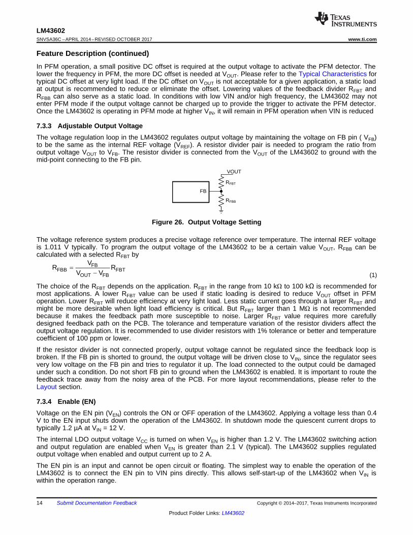
3 DescriptionThe LM43602 regulator is an easy-to-usesynchronous step-down DC-DC converter capable ofdriving up to 2 A of load current from an input voltageranging from 3.5 V to 36 V (42-V absolute maximum).The LM43602 provides exceptional efficiency, outputaccuracy, and dropout voltage in a very small solutionsize. An extended family is available in 0.5-A, 1-A,and 3-A load current options in pin-to-pin compatiblepackages. Peak current-mode control is employed toachieve simple control loop compensation and cycle-by-cycle current limiting. Optional features such asprogrammable switching frequency, synchronization,power-good flag, precision enable, internal soft start,extendable soft start, and tracking provide a flexibleand easy-to-use platform for a wide range ofapplications. Discontinuous conduction and automaticfrequency modulation at light loads improve light-loadefficiency. The family requires few externalcomponents and terminal arrangement allows simple,optimum PCB layout. Protection features includethermal shutdown, VCC undervoltage lockout, cycle-by-cycle current limit, and output short circuitprotection. The LM43602 device is available in a 16-lead HTSSOP package (5.1 mm × 6.6 mm × 1.2 mm)and 16-pin VSON package with wettable flanks.
Device InformationORDER NUMBER PACKAGE BODY SIZE
LM43602HTSSOP (16) 5.10 mm × 6.60 mmVSON (16) 4.10 mm × 5.10 mm
Simplified SchematicLM43602PWPEVM Radiated Emission Graph
12VIN to 3.3 VOUT,FS = 500 kHz, IOUT = 2 A
2
LM43602SNVSA36C –APRIL 2014–REVISED OCTOBER 2017 www.ti.com
Product Folder Links: LM43602
Submit Documentation Feedback Copyright © 2014–2017, Texas Instruments Incorporated
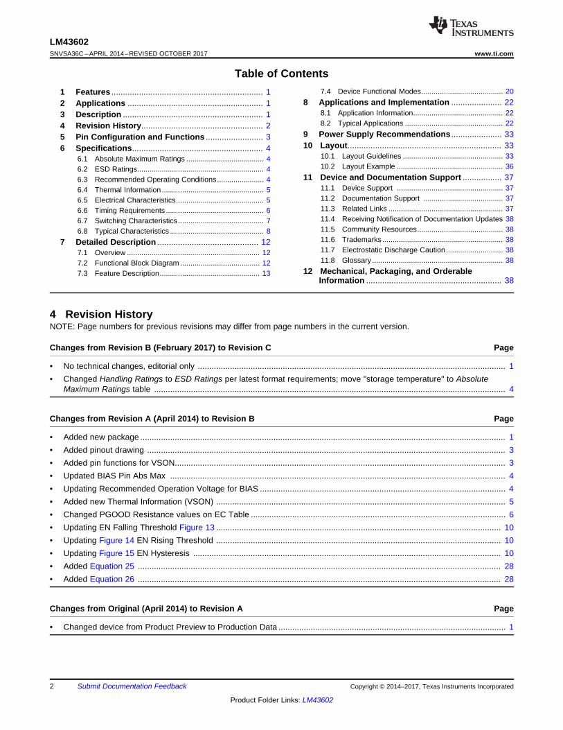
Table of Contents1 Features .................................................................. 12 Applications ........................................................... 13 Description ............................................................. 14 Revision History..................................................... 25 Pin Configuration and Functions ......................... 36 Specifications......................................................... 4
6.1 Absolute Maximum Ratings ...................................... 46.2 ESD Ratings.............................................................. 46.3 Recommended Operating Conditions....................... 46.4 Thermal Information .................................................. 56.5 Electrical Characteristics........................................... 56.6 Timing Requirements ................................................ 66.7 Switching Characteristics .......................................... 76.8 Typical Characteristics .............................................. 8
7 Detailed Description ............................................ 127.1 Overview ................................................................. 127.2 Functional Block Diagram ....................................... 127.3 Feature Description................................................. 13
7.4 Device Functional Modes........................................ 208 Applications and Implementation ...................... 22
8.1 Application Information............................................ 228.2 Typical Applications ................................................ 22
9 Power Supply Recommendations ...................... 3310 Layout................................................................... 33
10.1 Layout Guidelines ................................................. 3310.2 Layout Example .................................................... 36
11 Device and Documentation Support ................. 3711.1 Device Support .................................................... 3711.2 Documentation Support ....................................... 3711.3 Related Links ........................................................ 3711.4 Receiving Notification of Documentation Updates 3811.5 Community Resources.......................................... 3811.6 Trademarks ........................................................... 3811.7 Electrostatic Discharge Caution............................ 3811.8 Glossary ................................................................ 38
12 Mechanical, Packaging, and OrderableInformation ........................................................... 38
4 Revision HistoryNOTE: Page numbers for previous revisions may differ from page numbers in the current version.
Changes from Revision B (February 2017) to Revision C Page
• No technical changes, editorial only ...................................................................................................................................... 1• Changed Handling Ratings to ESD Ratings per latest format requirements; move "storage temperature" to Absolute
Maximum Ratings table ......................................................................................................................................................... 4
Changes from Revision A (April 2014) to Revision B Page
• Added new package ............................................................................................................................................................... 1• Added pinout drawing ............................................................................................................................................................ 3• Added pin functions for VSON................................................................................................................................................ 3• Updated BIAS Pin Abs Max .................................................................................................................................................. 4• Updating Recommended Operation Voltage for BIAS ........................................................................................................... 4• Added new Thermal Information (VSON) .............................................................................................................................. 5• Changed PGOOD Resistance values on EC Table ............................................................................................................... 6• Updating EN Falling Threshold Figure 13 ............................................................................................................................ 10• Updating Figure 14 EN Rising Threshold ............................................................................................................................ 10• Updating Figure 15 EN Hysteresis ...................................................................................................................................... 10• Added Equation 25 .............................................................................................................................................................. 28• Added Equation 26 .............................................................................................................................................................. 28
Changes from Original (April 2014) to Revision A Page
• Changed device from Product Preview to Production Data ................................................................................................... 1
SW
VIN
PGND
CBOOT
VCC
BIAS
SYNC
RT PGOOD
EN
SS/TRK
FB
SW PGND
VINPAD
1 16
2
3
4
5
6
8
7
9
15
14
13
12
11
10
SW
SW
VIN
PGND
CBOOT
VCC
BIAS
SYNC
RTPGOOD
EN
SS/TRK
AGND
FB
SW PGND
VINPAD
1 16
2
3
4
5
6
87
9
15
14
13
12
11
10
3
LM43602www.ti.com SNVSA36C –APRIL 2014–REVISED OCTOBER 2017
Product Folder Links: LM43602
Submit Documentation FeedbackCopyright © 2014–2017, Texas Instruments Incorporated
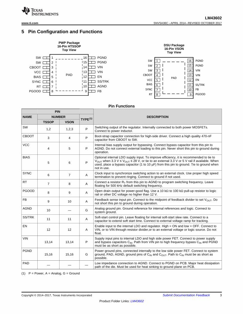
5 Pin Configuration and Functions
PWP Package16-Pin HTSSOP
Top ViewDSU Package16-Pin VSON
Top View
(1) P = Power, A = Analog, G = Ground
Pin FunctionsPIN
DESCRIPTIONNAME NUMBERTYPE (1)
TSSOP VSONSW 1,2 1,2,3 P Switching output of the regulator. Internally connected to both power MOSFETs.
Connect to power inductor.CBOOT 3 4 P Boot-strap capacitor connection for high-side driver. Connect a high quality 470-nF
capacitor from CBOOT to SW.VCC
4 5 PInternal bias supply output for bypassing. Connect bypass capacitor from this pin toAGND. Do not connect external loading to this pin. Never short this pin to ground duringoperation.
BIAS
5 6 P
Optional internal LDO supply input. To improve efficiency, it is recommended to tie toVOUT when 3.3 V ≤ VOUT ≤ 28 V, or tie to an external 3.3 V or 5 V rail if available. Whenused, place a bypass capacitor (1 to 10 µF) from this pin to ground. Tie to ground whennot in use.
SYNC 6 7 A Clock input to synchronize switching action to an external clock. Use proper high speedtermination to prevent ringing. Connect to ground if not used.
RT 7 8 A Connect a resistor RT from this pin to AGND to program switching frequency. Leavefloating for 500 kHz default switching frequency.
PGOOD 8 9 A Open drain output for power-good flag. Use a 10 kΩ to 100 kΩ pull-up resistor to logicrail or other DC voltage no higher than 12 V.
FB 9 10 A Feedback sense input pin. Connect to the midpoint of feedback divider to set VOUT. Donot short this pin to ground during operation.
AGND 10 — G Analog ground pin. Ground reference for internal references and logic. Connect tosystem ground.
SS/TRK 11 11 A Soft-start control pin. Leave floating for internal soft-start slew rate. Connect to acapacitor to extend soft start time. Connect to external voltage ramp for tracking.
EN12 12 A
Enable input to the internal LDO and regulator. High = ON and low = OFF. Connect toVIN, or to VIN through resistor divider,or to an external voltage or logic source. Do notfloat.
VIN13,14 13,14 P
Supply input pins to internal LDO and high side power FET. Connect to power supplyand bypass capacitors CIN. Path from VIN pin to high frequency bypass CIN and PGNDmust be as short as possible.
PGND15,16 15,16 G
Power ground pins, connected internally to the low side power FET. Connect to systemground, PAD, AGND, ground pins of CIN and COUT. Path to CIN must be as short aspossible.
PAD — — — Low impedance connection to AGND. Connect to PGND on PCB. Major heat dissipationpath of the die. Must be used for heat sinking to ground plane on PCB.
4
LM43602SNVSA36C –APRIL 2014–REVISED OCTOBER 2017 www.ti.com
Product Folder Links: LM43602
Submit Documentation Feedback Copyright © 2014–2017, Texas Instruments Incorporated
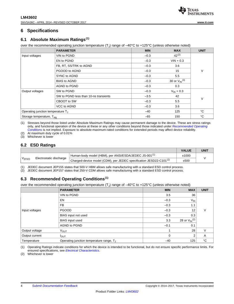
(1) Stresses beyond those listed under Absolute Maximum Ratings may cause permanent damage to the device. These are stress ratingsonly, and functional operation of the device at these or any other conditions beyond those indicated under Recommended OperatingConditions is not implied. Exposure to absolute-maximum-rated conditions for extended periods may affect device reliability.
(2) At maximum duty cycle of 0.01%(3) Whichever is lower
6 Specifications
6.1 Absolute Maximum Ratings (1)
over the recommended operating junction temperature (TJ) range of –40°C to +125°C (unless otherwise noted)PARAMETER MIN MAX UNIT
Input voltages VIN to PGND –0.3 42 (2)
V
EN to PGND –0.3 VIN + 0.3FB, RT, SS/TRK to AGND –0.3 3.6PGOOD to AGND –0.3 15SYNC to AGND –0.3 5.5BIAS to AGND –0.3 30 or VIN
(3)
AGND to PGND –0.3 0.3Output voltages SW to PGND –0.3 VIN + 0.3
VSW to PGND less than 10-ns transients –3.5 42CBOOT to SW –0.3 5.5VCC to AGND –0.3 3.6
Operating junction temperature TJ –40 125 °CStorage temperature, Tstg –65 150 °C
(1) JEDEC document JEP155 states that 500-V HBM allows safe manufacturing with a standard ESD control process.(2) JEDEC document JEP157 states that 250-V CDM allows safe manufacturing with a standard ESD control process.
6.2 ESD RatingsVALUE UNIT
V(ESD) Electrostatic dischargeHuman-body model (HBM), per ANSI/ESDA/JEDEC JS-001 (1) ±1000
VCharged-device model (CDM), per JEDEC specification JESD22-C101 (2) ±500
(1) Operating Ratings indicate conditions for which the device is intended to be functional, but do not ensure specific performance limits. Forensured specifications, see Electrical Characteristics.
(2) Whichever is lower
6.3 Recommended Operating Conditions (1)
over the recommended operating junction temperature (TJ) range of –40°C to +125°C (unless otherwise noted)PARAMETER MIN MAX UNIT
Input voltages
VIN to PGND 3.5 36
V
EN –0.3 VIN
FB –0.3 1.1PGOOD –0.3 12BIAS input not used –0.3 0.3BIAS input used 3.3 28 or VIN
(2)
AGND to PGND –0.1 0.1Output voltage VOUT 1 28 VOutput current IOUT 0 2 ATemperature Operating junction temperature range, TJ –40 125 °C
5
LM43602www.ti.com SNVSA36C –APRIL 2014–REVISED OCTOBER 2017
Product Folder Links: LM43602
Submit Documentation FeedbackCopyright © 2014–2017, Texas Instruments Incorporated
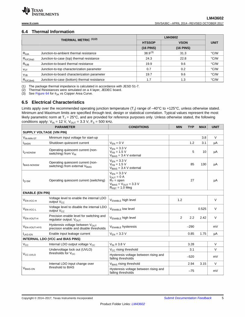
(1) The package thermal impedance is calculated in accordance with JESD 51-7.(2) Thermal Resistances were simulated on a 4 layer, JEDEC board.(3) See Figure 64 for θJA vs Copper Area Curve.
6.4 Thermal Information
THERMAL METRIC (1) (2) LM43602UNITHTSSOP VSON
(16 PINS) (16 PINS)RθJA Junction-to-ambient thermal resistance 38.9 (3) 31.3 °C/WRθJC(top) Junction-to-case (top) thermal resistance 24.3 22.8 °C/WRθJB Junction-to-board thermal resistance 19.9 9.6 °C/WψJT Junction-to-top characterization parameter 0.7 0.2 °C/WψJB Junction-to-board characterization parameter 19.7 9.6 °C/WRθJC(bot) Junction-to-case (bottom) thermal resistance 1.7 1.3 °C/W
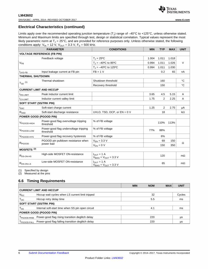
6.5 Electrical CharacteristicsLimits apply over the recommended operating junction temperature (TJ) range of –40°C to +125°C, unless otherwise stated.Minimum and Maximum limits are specified through test, design or statistical correlation. Typical values represent the mostlikely parametric norm at TJ = 25°C, and are provided for reference purposes only. Unless otherwise stated, the followingconditions apply: VIN = 12 V, VOUT = 3.3 V, FS = 500 kHz.
PARAMETER CONDITIONS MIN TYP MAX UNITSUPPLY VOLTAGE (VIN PIN)VIN-MIN-ST Minimum input voltage for start-up 3.8 VISHDN Shutdown quiescent current VEN = 0 V 1.2 3.1 µA
IQ-NONSWOperating quiescent current (non-switching) from VIN
VEN = 3.3 VVFB = 1.5 VVBIAS = 3.4 V external
5 10 µA
IBIAS-NONSWOperating quiescent current (non-switching) from external VBIAS
VEN = 3.3 VVFB = 1.5 VVBIAS = 3.4 V external
85 130 µA
IQ-SW Operating quiescent current (switching)
VEN = 3.3 VIOUT = 0 ART = openVBIAS = VOUT = 3.3 VRFBT = 1.0 Meg
27 µA
ENABLE (EN PIN)
VEN-VCC-HVoltage level to enable the internal LDOoutput VCC
VENABLE high level 1.2 V
VEN-VCC-LVoltage level to disable the internal LDOoutput VCC
VENABLE low level 0.525 V
VEN-VOUT-HPrecision enable level for switching andregulator output: VOUT
VENABLE high level 2 2.2 2.42 V
VEN-VOUT-HYSHysteresis voltage between VOUTprecision enable and disable thresholds VENABLE hysteresis –290 mV
ILKG-EN Enable input leakage current VEN = 3.3 V 0.85 1.75 µAINTERNAL LDO (VCC and BIAS PINS)VCC Internal LDO output voltage VCC VIN ≥ 3.8 V 3.28 V
VCC-UVLO
Undervoltage lock out (UVLO)thresholds for VCC
VCC rising threshold 3.1 VHysteresis voltage between rising andfalling thresholds –520 mV
VBIAS-ON
Internal LDO input change overthreshold to BIAS
VBIAS rising threshold 2.94 3.15 VHysteresis voltage between rising andfalling thresholds –75 mV
6
LM43602SNVSA36C –APRIL 2014–REVISED OCTOBER 2017 www.ti.com
Product Folder Links: LM43602
Submit Documentation Feedback Copyright © 2014–2017, Texas Instruments Incorporated
Electrical Characteristics (continued)Limits apply over the recommended operating junction temperature (TJ) range of –40°C to +125°C, unless otherwise stated.Minimum and Maximum limits are specified through test, design or statistical correlation. Typical values represent the mostlikely parametric norm at TJ = 25°C, and are provided for reference purposes only. Unless otherwise stated, the followingconditions apply: VIN = 12 V, VOUT = 3.3 V, FS = 500 kHz.
PARAMETER CONDITIONS MIN TYP MAX UNIT
(1) Specified by design(2) Measured at the pins
VOLTAGE REFERENCE (FB PIN)
VFB
Feedback voltage TJ = 25ºC 1.004 1.011 1.018VTJ = –40ºC to 85ºC 0.994 1.011 1.026
TJ = –40ºC to 125ºC 0.994 1.011 1.030ILKG-FB Input leakage current at FB pin FB = 1 V 0.2 65 nATHERMAL SHUTDOWN
TSD(1) Thermal shutdown Shutdown threshold 160 °C
Recovery threshold 150 °CCURRENT LIMIT AND HICCUPIHS-LIMIT Peak inductor current limit 3.65 4.5 5.15 AILS-LIMIT Inductor current valley limit 1.75 2 2.25 ASOFT START (SS/TRK PIN)ISSC Soft-start charge current 1.25 2 2.75 µARSSD Soft-start discharge resistance UVLO, TSD, OCP, or EN = 0 V 18 kΩPOWER GOOD (PGOOD PIN)
VPGOOD-HIGHPower-good flag overvoltage trippingthreshold
% of FB voltage 110% 113%
VPGOOD-LOWPower-good flag undervoltage trippingthreshold
% of FB voltage 77% 88%
VPGOOD-HYS Power-good flag recovery hysteresis % of FB voltage 6%
RPGOODPGOOD pin pulldown resistance whenpower bad
VEN = 3.3 V 69 150Ω
VEN = 0 V 150 350MOSFETS (2)
RDS-ON-HSHigh-side MOSFET ON-resistance IOUT = 1 A
VBIAS = VOUT = 3.3 V 120 mΩ
RDS-ON-LSLow-side MOSFET ON-resistance IOUT = 1 A
VBIAS = VOUT = 3.3 V 65 mΩ
6.6 Timing RequirementsMIN NOM MAX UNIT
CURRENT LIMIT AND HICCUPNOC Hiccup wait cycles when LS current limit tripped 32 CyclesTOC Hiccup retry delay time 5.5 msSOFT START (SS/TRK PIN)TSS Internal soft-start time when SS pin open circuit 4.1 msPOWER GOOD (PGOOD PIN)TPGOOD-RISE Power-good flag rising transition deglitch delay 220 µsTPGOOD-FALL Power-good flag falling transition deglitch delay 220 µs
7
LM43602www.ti.com SNVSA36C –APRIL 2014–REVISED OCTOBER 2017
Product Folder Links: LM43602
Submit Documentation FeedbackCopyright © 2014–2017, Texas Instruments Incorporated
(1) Specified by design
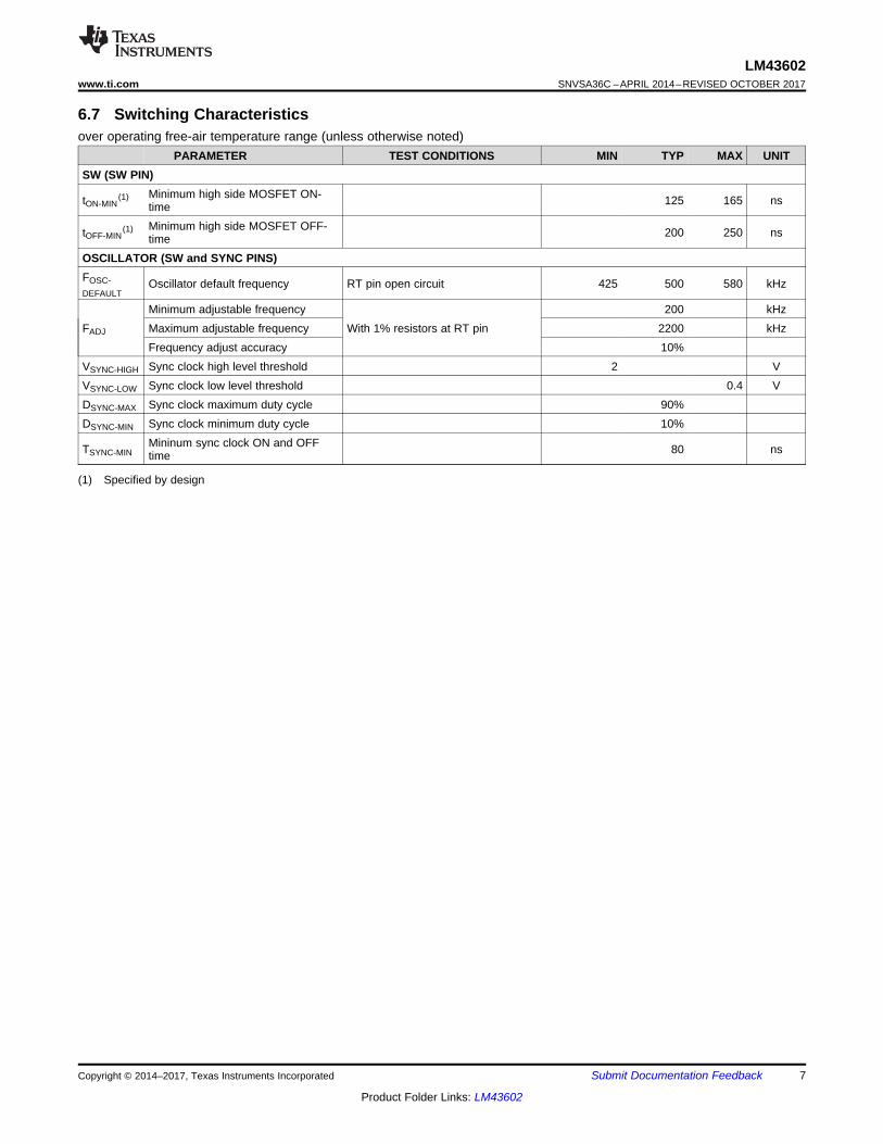
6.7 Switching Characteristicsover operating free-air temperature range (unless otherwise noted)
PARAMETER TEST CONDITIONS MIN TYP MAX UNITSW (SW PIN)
tON-MIN(1) Minimum high side MOSFET ON-
time 125 165 ns
tOFF-MIN(1) Minimum high side MOSFET OFF-
time 200 250 ns
OSCILLATOR (SW and SYNC PINS)FOSC-DEFAULT
Oscillator default frequency RT pin open circuit 425 500 580 kHz
FADJ
Minimum adjustable frequencyWith 1% resistors at RT pin
200 kHzMaximum adjustable frequency 2200 kHzFrequency adjust accuracy 10%
VSYNC-HIGH Sync clock high level threshold 2 VVSYNC-LOW Sync clock low level threshold 0.4 VDSYNC-MAX Sync clock maximum duty cycle 90%DSYNC-MIN Sync clock minimum duty cycle 10%
TSYNC-MINMininum sync clock ON and OFFtime 80 ns
40
50
60
70
80
90
100
0 0.5 1 1.5 2
Effi
cien
cy (
%)
Current (A)
12VIN
24VIN
C001
40
50
60
70
80
90
100
0.001 0.01 0.1 1
Effi
cien
cy (
%)
Current (A)
12VIN
24VIN
C001
40
50
60
70
80
90
100
0.001 0.01 0.1 1
Effi
cien
cy (
%)
Current (A)
5VIN
12VIN
24VIN
C001
40
50
60
70
80
90
100
0.001 0.01 0.1 1
Effi
cien
cy (
%)
Current (A)
12VIN
24VIN
C001
40
50
60
70
80
90
100
0.001 0.01 0.1 1
Effi
cien
cy (
%)
Current (A)
5VIN
12VIN
24VIN
C001
40
50
60
70
80
90
100
0 0.5 1 1.5 2
Effi
cien
cy (
%)
Current (A)
5VIN
12VIN
24VIN
C001
8
LM43602SNVSA36C –APRIL 2014–REVISED OCTOBER 2017 www.ti.com
Product Folder Links: LM43602
Submit Documentation Feedback Copyright © 2014–2017, Texas Instruments Incorporated
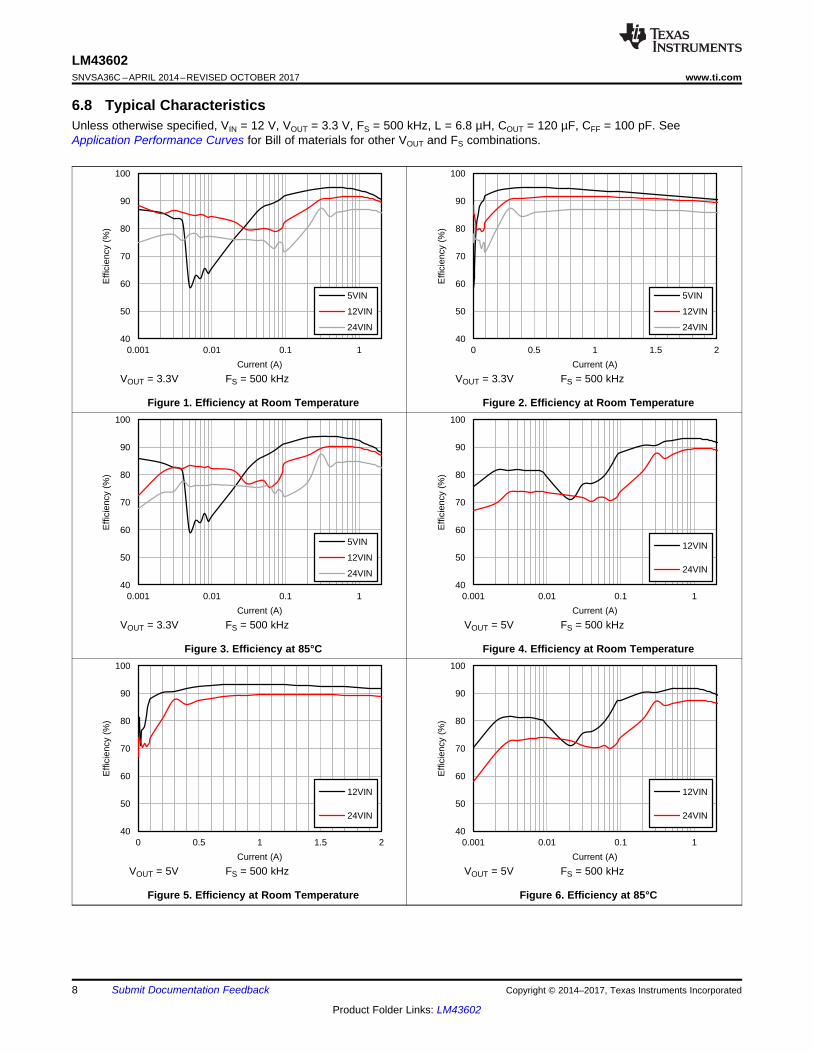
6.8 Typical CharacteristicsUnless otherwise specified, VIN = 12 V, VOUT = 3.3 V, FS = 500 kHz, L = 6.8 µH, COUT = 120 µF, CFF = 100 pF. SeeApplication Performance Curves for Bill of materials for other VOUT and FS combinations.
VOUT = 3.3V FS = 500 kHz
Figure 1. Efficiency at Room Temperature
VOUT = 3.3V FS = 500 kHz
Figure 2. Efficiency at Room Temperature
VOUT = 3.3V FS = 500 kHz
Figure 3. Efficiency at 85°C
VOUT = 5V FS = 500 kHz
Figure 4. Efficiency at Room Temperature
VOUT = 5V FS = 500 kHz
Figure 5. Efficiency at Room Temperature
VOUT = 5V FS = 500 kHz
Figure 6. Efficiency at 85°C
1000
10000
100000
1000000
3.5 3.7 3.9 4.1 4.3 4.5
FR
EQ
UE
NC
Y (
Hz)
VIN (V)
0.1A
0.5A
1A
1.5A
2A
C007
10000
100000
1000000
5.00 5.20 5.40 5.60 5.80 6.00 6.20 6.40 6.60 6.80 7.00
Fre
quen
cy (
Hz)
VIN (V)
0.1A
0.5A
1A
1.5A
2A
C007
2.9
3.0
3.1
3.2
3.3
3.4
3.5
3.5 3.7 3.9 4.1 4.3 4.5
VO
UT
(V
)
VIN (V)
0.1A
0.5A
1A
1.5A
2A
C007
4.0
4.2
4.4
4.6
4.8
5.0
5.2
5.4
5.00 5.20 5.40 5.60 5.80 6.00 6.20 6.40 6.60 6.80 7.00
VO
UT
(V
)
VIN (V)
0.1A 0.5A 1A 1.5A 2A
C007
3.20
3.22
3.24
3.26
3.28
3.30
3.32
3.34
3.36
3.38
3.40
0.001 0.01 0.1 1
VO
UT
(V
)
Current (A)
5VIN
12VIN
24VIN
C001
4.75
4.80
4.85
4.90
4.95
5.00
5.05
5.10
5.15
5.20
5.25
0.001 0.01 0.1 1
VO
UT
(V
)
Current (A)
8VIN
12VIN
24VIN
C004
9
LM43602www.ti.com SNVSA36C –APRIL 2014–REVISED OCTOBER 2017
Product Folder Links: LM43602
Submit Documentation FeedbackCopyright © 2014–2017, Texas Instruments Incorporated
Typical Characteristics (continued)Unless otherwise specified, VIN = 12 V, VOUT = 3.3 V, FS = 500 kHz, L = 6.8 µH, COUT = 120 µF, CFF = 100 pF. SeeApplication Performance Curves for Bill of materials for other VOUT and FS combinations.
VOUT = 3.3V FS = 500 kHz
Figure 7. VOUT Regulation
VOUT = 5V FS = 500 kHz
Figure 8. VOUT Regulation
VOUT = 3.3V FS = 500 kHz
Figure 9. Dropout Curve
VOUT = 5V FS = 500 kHz
Figure 10. Dropout Curve
VOUT = 3.3V FS = 500 kHz
Figure 11. Frequency vs VIN
VOUT = 5V FS = 500 kHz
Figure 12. Frequency vs VIN
3.600
3.700
3.800
3.900
4.000
4.100
4.200
±40 ±25 ±10 5 20 35 50 65 80 95 110 125
HS
Cur
rent
Lim
it (A
)
Temperature (deg C) C001
1.800
1.900
2.000
2.100
2.200
±40 ±25 ±10 5 20 35 50 65 80 95 110 125
LS C
urre
nt L
imit
(A)
Temperature (deg C) C001
250
260
270
280
290
300
310
±40 ±25 ±10 5 20 35 50 65 80 95 110 125
EN
Hys
tere
sis
(mV
)
Temperature (deg C) C001
1.000
1.005
1.010
1.015
1.020
±40 ±25 ±10 5 20 35 50 65 80 95 110 125
FB
Vol
tage
(V
)
Temperature (deg C) C001
1.600
1.650
1.700
1.750
1.800
1.850
1.900
1.950
2.000
±40 ±25 ±10 5 20 35 50 65 80 95 110 125
EN
Vol
tage
(V
)
Temperature (deg C) C001
1.900
1.950
2.000
2.050
2.100
2.150
2.200
±40 ±25 ±10 5 20 35 50 65 80 95 110 125
EN
Vol
tage
(V
)
Temperature (deg C) C001
10
LM43602SNVSA36C –APRIL 2014–REVISED OCTOBER 2017 www.ti.com
Product Folder Links: LM43602
Submit Documentation Feedback Copyright © 2014–2017, Texas Instruments Incorporated
Typical Characteristics (continued)Unless otherwise specified, VIN = 12 V, VOUT = 3.3 V, FS = 500 kHz, L = 6.8 µH, COUT = 120 µF, CFF = 100 pF. SeeApplication Performance Curves for Bill of materials for other VOUT and FS combinations.
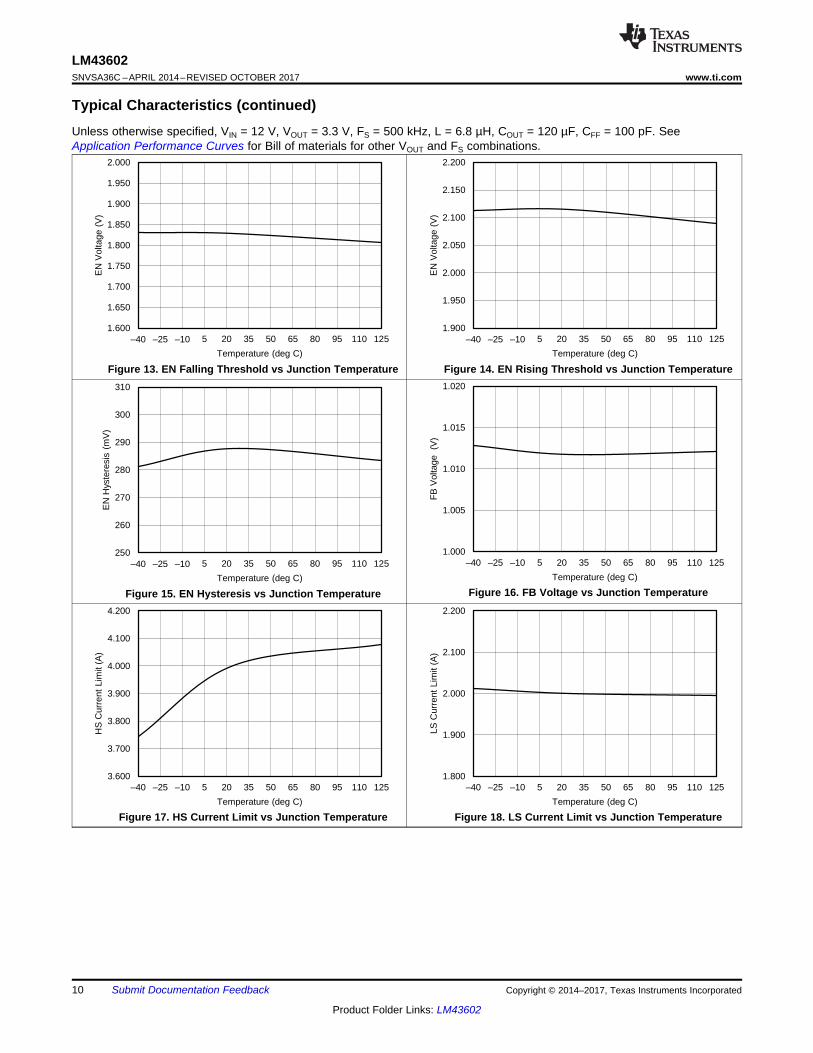
Figure 13. EN Falling Threshold vs Junction Temperature Figure 14. EN Rising Threshold vs Junction Temperature
Figure 15. EN Hysteresis vs Junction Temperature Figure 16. FB Voltage vs Junction Temperature
Figure 17. HS Current Limit vs Junction Temperature Figure 18. LS Current Limit vs Junction Temperature
86.0
87.0
88.0
89.0
90.0
91.0
92.0
±40 ±25 ±10 5 20 35 50 65 80 95 110 125
Per
cent
age
of F
B V
olta
ge
(%)
Temperature (deg C) C001
92.0
93.0
94.0
95.0
96.0
97.0
98.0
±40 ±25 ±10 5 20 35 50 65 80 95 110 125
Per
cent
age
of F
B V
olta
ge
(%)
Temperature (deg C) C001
109.0
109.5
110.0
110.5
111.0
111.5
112.0
±40 ±25 ±10 5 20 35 50 65 80 95 110 125
Per
cent
age
of F
B V
olta
ge
(%)
Temperature (deg C) C001
104.0
104.5
105.0
105.5
106.0
106.5
107.0
±40 ±25 ±10 5 20 35 50 65 80 95 110 125
Per
cent
age
of F
B V
olta
ge
(%)
Temperature (deg C) C001
90
100
110
120
130
140
150
160
170
180
190
±40 ±25 ±10 5 20 35 50 65 80 95 110 125
HS
Rds
-on
(m
)
Temperature (deg C) C001
40
45
50
55
60
65
70
75
80
85
90
±40 ±25 ±10 5 20 35 50 65 80 95 110 125
LS R
ds-o
n (m
)
Temperature (deg C) C001
11
LM43602www.ti.com SNVSA36C –APRIL 2014–REVISED OCTOBER 2017
Product Folder Links: LM43602
Submit Documentation FeedbackCopyright © 2014–2017, Texas Instruments Incorporated
Typical Characteristics (continued)Unless otherwise specified, VIN = 12 V, VOUT = 3.3 V, FS = 500 kHz, L = 6.8 µH, COUT = 120 µF, CFF = 100 pF. SeeApplication Performance Curves for Bill of materials for other VOUT and FS combinations.
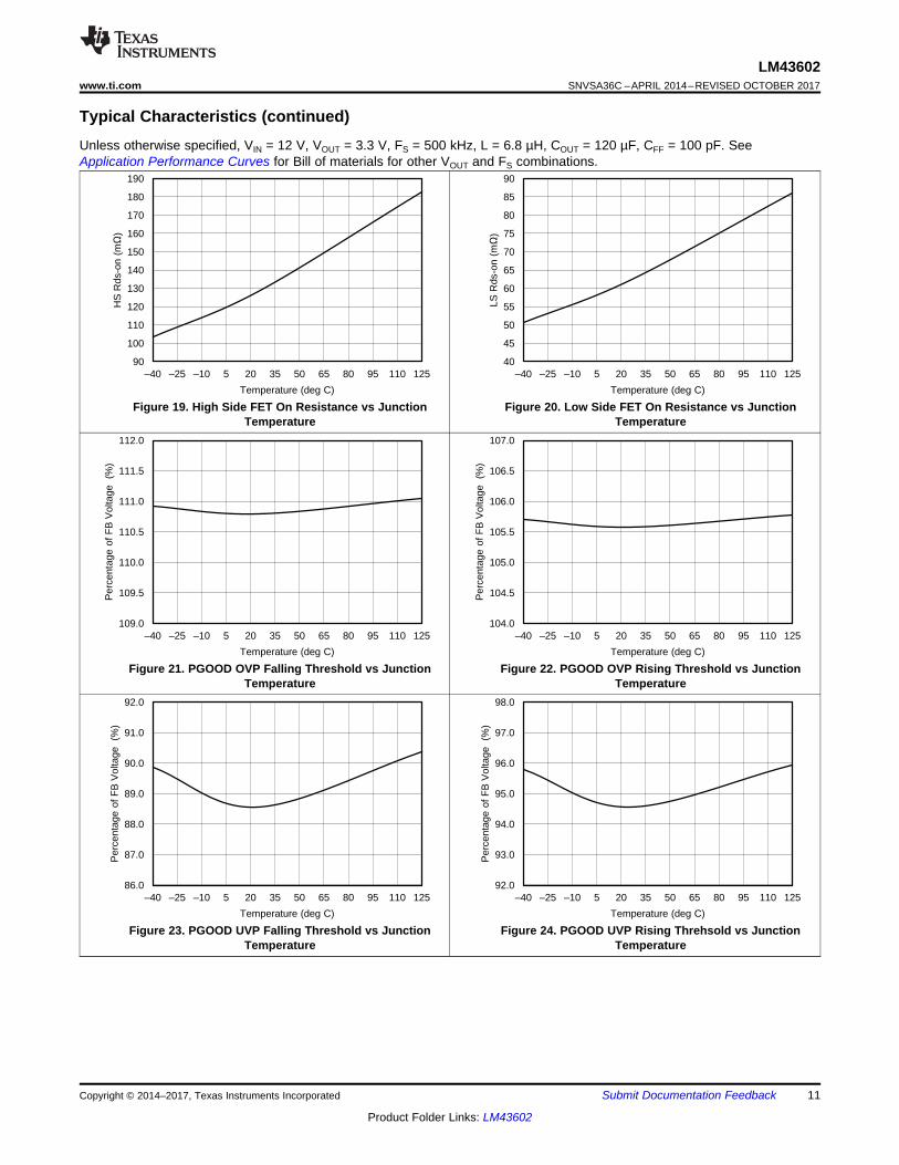
Figure 19. High Side FET On Resistance vs JunctionTemperature
Figure 20. Low Side FET On Resistance vs JunctionTemperature
Figure 21. PGOOD OVP Falling Threshold vs JunctionTemperature
Figure 22. PGOOD OVP Rising Threshold vs JunctionTemperature
Figure 23. PGOOD UVP Falling Threshold vs JunctionTemperature
Figure 24. PGOOD UVP Rising Threhsold vs JunctionTemperature
PrecisionEnable
VCC Enable
SlopeComp
LDO
HICCUP Detector
PFM Detector
TSD
Oscillator
PWM CONTROL LOGIC
Freq Foldback
Zero Cross
UVLO
CBOOT
VIN
BIAS
PGOOD
ENABLE
AGND
PGNDSYNC
VCC
SW
FB
HS I Sense
RT
ISSC
+±
LS I Sense
PGood
PGood
FB
SS/TRK
+
OV/UV Detector
REF EA
Internal SS
RC
CC
+ ±
12
LM43602SNVSA36C –APRIL 2014–REVISED OCTOBER 2017 www.ti.com
Product Folder Links: LM43602
Submit Documentation Feedback Copyright © 2014–2017, Texas Instruments Incorporated
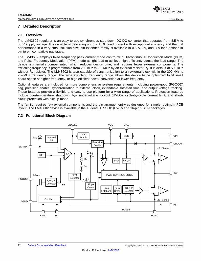
7 Detailed Description
7.1 OverviewThe LM43602 regulator is an easy to use synchronous step-down DC-DC converter that operates from 3.5 V to36 V supply voltage. It is capable of delivering up to 2 A DC load current with exceptional efficiency and thermalperformance in a very small solution size. An extended family is available in 0.5 A, 1A, and 3 A load options inpin to pin compatible packages.
The LM43602 employs fixed frequency peak current mode control with Discontinuous Conduction Mode (DCM)and Pulse Frequency Modulation (PFM) mode at light load to achieve high efficiency across the load range. Thedevice is internally compensated, which reduces design time, and requires fewer external components. Theswitching frequency is programmable from 200 kHz to 2.2 MHz by an external resistor RT. It is default at 500 kHzwithout RT resistor. The LM43602 is also capable of synchronization to an external clock within the 200-kHz to2.2-MHz frequency range. The wide switching frequency range allows the device to be optimized to fit smallboard space at higher frequency, or high efficient power conversion at lower frequency.
Optional features are included for more comprehensive system requirements, including power-good (PGOOD)flag, precision enable, synchronization to external clock, extendable soft-start time, and output voltage tracking.These features provide a flexible and easy to use platform for a wide range of applications. Protection featuresinclude overtemperature shutdown, VCC undervoltage lockout (UVLO), cycle-by-cycle current limit, and short-circuit protection with hiccup mode.
The family requires few external components and the pin arrangement was designed for simple, optimum PCBlayout. The LM43602 device is available in the 16-lead HTSSOP (PWP) and 16-pin VSON packages.
7.2 Functional Block Diagram
0
0
VIN
-VD1
tON
t
tIndu
ctor
Cur
rent
D = tON / TSW
VSW
tOFF
TSWiL
SW
Vol
tage
ûiLIOUT
ILPK
13
LM43602www.ti.com SNVSA36C –APRIL 2014–REVISED OCTOBER 2017
Product Folder Links: LM43602
Submit Documentation FeedbackCopyright © 2014–2017, Texas Instruments Incorporated
7.3 Feature Description
7.3.1 Fixed Frequency Peak Current-Mode Controlled Step-Down RegulatorThe following operating description of the LM43602 will refer to the Functional Block Diagram and to thewaveforms in Figure 25. The LM43602 is a step-down Buck regulator with both high-side (HS) switch and low-side (LS) switch (synchronous rectifier) integrated. The LM43602 supplies a regulated output voltage by turningon the HS and LS NMOS switches with controlled ON time. During the HS switch ON time, the SW pin voltageVSW swings up to approximately VIN, and the inductor current iL increases with a linear slope (VIN - VOUT) / L.When the HS switch is turned off by the control logic, the LS switch is turned on after a anti-shoot-through deadtime. Inductor current discharges through the LS switch with a slope of -VOUT / L. The control parameter of buckconverters are defined as Duty Cycle D = tON / TSW, where tON is the HS switch ON time and TSW is the switchingperiod. The regulator control loop maintains a constant output voltage by adjusting the duty cycle D. In an idealBuck converter, where losses are ignored, D is proportional to the output voltage and inversely proportional tothe input voltage: D = VOUT / VIN.
Figure 25. SW Node and Inductor Current Waveforms in Continuous Conduction Mode (CCM)
The LM43602 synchronous Buck converter employs peak current mode control topology. A voltage feedbackloop is used to get accurate DC voltage regulation by adjusting the peak current command based on voltageoffset. The peak inductor current is sensed from the HS switch and compared to the peak current to control theON time of the HS switch. The voltage feedback loop is internally compensated, which allows for fewer externalcomponents, makes it easy to design, and provides stable operation with almost any combination of outputcapacitors. The regulator operates with fixed switching frequency in Continuous Conduction Mode (CCM) andDiscontinuous Conduction Mode (DCM). At very light load, the LM43602 will operate in PFM to maintain highefficiency and the switching frequency will decrease with reduced load current.
7.3.2 Light Load OperationDCM operation is employed in the LM43602 when the inductor current valley reaches zero. The LM43602 will bein DCM when load current is less than half of the peak-to-peak inductor current ripple in CCM. In DCM, the LSswitch is turned off when the inductor current reaches zero. Switching loss is reduced by turning off the LS FETat zero current and the conduction loss is lowered by not allowing negative current conduction. Power conversionefficiency is higher in DCM than CCM under the same conditions.
In DCM, the HS switch ON time will reduce with lower load current. When either the minimum HS switch ON time(tON-MIN) or the minimum peak inductor current (IPEAK-MIN) is reached, the switching frequency will decrease tomaintain regulation. At this point, the LM43602 operates in PFM. In PFM, switching frequency is decreased bythe control loop when load current reduces to maintain output voltage regulation. Switching loss is furtherreduced in PFM operation due to less frequent switching actions.
FBFBB FBT
OUT FB
VR R
V V
FB
RFBT
RFBB
VOUT
14
LM43602SNVSA36C –APRIL 2014–REVISED OCTOBER 2017 www.ti.com
Product Folder Links: LM43602
Submit Documentation Feedback Copyright © 2014–2017, Texas Instruments Incorporated
Feature Description (continued)In PFM operation, a small positive DC offset is required at the output voltage to activate the PFM detector. Thelower the frequency in PFM, the more DC offset is needed at VOUT. Please refer to the Typical Characteristics fortypical DC offset at very light load. If the DC offset on VOUT is not acceptable for a given application, a static loadat output is recommended to reduce or eliminate the offset. Lowering values of the feedback divider RFBT andRFBB can also serve as a static load. In conditions with low VIN and/or high frequency, the LM43602 may notenter PFM mode if the output voltage cannot be charged up to provide the trigger to activate the PFM detector.Once the LM43602 is operating in PFM mode at higher VIN, it will remain in PFM operation when VIN is reduced
7.3.3 Adjustable Output VoltageThe voltage regulation loop in the LM43602 regulates output voltage by maintaining the voltage on FB pin ( VFB)to be the same as the internal REF voltage (VREF). A resistor divider pair is needed to program the ratio fromoutput voltage VOUT to VFB. The resistor divider is connected from the VOUT of the LM43602 to ground with themid-point connecting to the FB pin.
Figure 26. Output Voltage Setting
The voltage reference system produces a precise voltage reference over temperature. The internal REF voltageis 1.011 V typically. To program the output voltage of the LM43602 to be a certain value VOUT, RFBB can becalculated with a selected RFBT by
(1)
The choice of the RFBT depends on the application. RFBT in the range from 10 kΩ to 100 kΩ is recommended formost applications. A lower RFBT value can be used if static loading is desired to reduce VOUT offset in PFMoperation. Lower RFBT will reduce efficiency at very light load. Less static current goes through a larger RFBT andmight be more desirable when light load efficiency is critical. But RFBT larger than 1 MΩ is not recommendedbecause it makes the feedback path more susceptible to noise. Larger RFBT value requires more carefullydesigned feedback path on the PCB. The tolerance and temperature variation of the resistor dividers affect theoutput voltage regulation. It is recommended to use divider resistors with 1% tolerance or better and temperaturecoefficient of 100 ppm or lower.
If the resistor divider is not connected properly, output voltage cannot be regulated since the feedback loop isbroken. If the FB pin is shorted to ground, the output voltage will be driven close to VIN, since the regulator seesvery low voltage on the FB pin and tries to regulator it up. The load connected to the output could be damagedunder such a condition. Do not short FB pin to ground when the LM43602 is enabled. It is important to route thefeedback trace away from the noisy area of the PCB. For more layout recommendations, please refer to theLayout section.
7.3.4 Enable (EN)Voltage on the EN pin (VEN) controls the ON or OFF operation of the LM43602. Applying a voltage less than 0.4V to the EN input shuts down the operation of the LM43602. In shutdown mode the quiescent current drops totypically 1.2 µA at VIN = 12 V.
The internal LDO output voltage VCC is turned on when VEN is higher than 1.2 V. The LM43602 switching actionand output regulation are enabled when VEN is greater than 2.1 V (typical). The LM43602 supplies regulatedoutput voltage when enabled and output current up to 2 A.
The EN pin is an input and cannot be open circuit or floating. The simplest way to enable the operation of theLM43602 is to connect the EN pin to VIN pins directly. This allows self-start-up of the LM43602 when VIN iswithin the operation range.
SS SSC SSC I t u
VIN
ENABLE
RENT
RENB
15
LM43602www.ti.com SNVSA36C –APRIL 2014–REVISED OCTOBER 2017
Product Folder Links: LM43602
Submit Documentation FeedbackCopyright © 2014–2017, Texas Instruments Incorporated
Feature Description (continued)Many applications will benefit from the employment of an enable divider RENT and RENB in Figure 27 to establisha precision system UVLO level for the stage. System UVLO can be used for supplies operating from utility poweras well as battery power. It can be used for sequencing, ensuring reliable operation, or supply protection, suchas a battery. An external logic signal can also be used to drive EN input for system sequencing and protection.
Figure 27. System UVLO By Enable Dividers
7.3.5 VCC, UVLO and BIASThe LM43602 integrates an internal LDO to generate VCC for control circuitry and MOSFET drivers. The nominalvoltage for VCC is 3.2 V. The VCC pin is the output of the LDO must be properly bypassed. A high qualityceramic capacitor with 2.2 µF to 10 µF capacitance and 6.3 V or higher rated voltage should be placed as closeas possible to VCC and grounded to the exposed PAD and ground pins. The VCC output pin should not beloaded, left floating, or shorted to ground during operation. Shorting VCC to ground during operation may causedamage to the LM43602.
Under voltage lockout (UVLO) prevents the LM43602 from operating until the VCC voltage exceeds 3.15 V(typical). The VCC UVLO threshold has 575 mV of hysteresis (typically) to prevent undesired shuting down due totemperary VIN droops.
The internal LDO has two inputs: primary from VIN and secondary from BIAS input. The BIAS input powers theLDO when VBIAS is higher than the change-over threshold. Power loss of an LDO is calculated by ILDO * (VIN-LDO -VOUT-LDO). The higher the difference between the input and output voltages of the LDO, the more power lossoccur to supply the same output current. The BIAS input is designed to reduce the difference of the input andoutput voltages of the LDO to reduce power loss and improve LM43602 efficiency, especially at light load. It isrecommended to tie the BIAS pin to VOUT when VOUT ≥ 3.3 V. The BIAS pin should be grounded in applicationswith VOUT less than 3.3 V. BIAS input can also come from an external voltage source, if available, to reducepower loss. When used, a 1 µF to 10 µF high quality ceramic capacitor is recommended to bypass the BIAS pinto ground.
7.3.6 Soft-Start and Voltage Tracking (SS/TRK)The LM43602 has a flexible and easy to use start up rate control pin: SS/TRK. Soft-start feature is to preventinrush current impacting the LM43602 and its supply when power is first applied. Soft-start is achieved by slowlyramping up the target regulation voltage when the device is first enabled or powered up.
The simplest way to use the part is to leave the SS/TRK pin open circuit or floating. The LM43602 will employthe internal soft-start control ramp and start up to the regulated output voltage in 4.1 ms typically.
In applications with a large amount of output capacitors, or higher VOUT, or other special requirements the soft-start time can be extended by connecting an external capacitor CSS from SS/TRK pin to AGND. Extended soft-start time further reduces the supply current needed to charge up output capacitors and supply any outputloading. An internal current source (ISSC = 2.2 µA) charges CSS and generates a ramp from 0 V to VFB to controlthe ramp-up rate of the output voltage. For a desired soft start time tSS, the capacitance for CSS can be found by
(2)
The LM43602 is capable of start up into prebiased output conditions. When the inductor current reaches zero,the LS switch will be turned off to avoid negative current conduction. This operation mode is also called diodeemulation mode. It is built-in by the DCM operation in light loads. With prebiased output voltage, the LM43602will wait until the soft-start ramp allows regulation above the prebiased voltage and then follow the soft-start rampto regulation level.
Enable
Internal SS Ramp
Ext Tracking Signal to SS pin
VOUT
Enable
Internal SS Ramp
Ext Tracking Signal to SS pin
VOUT
SS/TRK
RTRT
RTRB
EXT RAMP
16
LM43602SNVSA36C –APRIL 2014–REVISED OCTOBER 2017 www.ti.com
Product Folder Links: LM43602
Submit Documentation Feedback Copyright © 2014–2017, Texas Instruments Incorporated
Feature Description (continued)When an external voltage ramp is applied to the SS/TRK pin, the LM43602 FB voltage follows the ramp if theramp magnitude is lower than the internal soft-start ramp. A resistor divider pair can be used on the externalcontrol ramp to the SS/TRK pin to program the tracking rate of the output voltage. The final voltage seen by theSS/TRK pin should not fall below 1.2 V to avoid abnormal operation.
Figure 28. Soft Start Tracking External Ramp
VOUT tracked to external voltage ramps has options of ramping up slower or faster than the internal voltage ramp.VFB always follows the lower potential of the internal voltage ramp and the voltage on the SS/TRK pin. Figure 29shows the case when VOUT ramps slower than the internal ramp, while Figure 30 shows when VOUT ramps fasterthan the internal ramp. Faster start up time may result in inductor current tripping current protection during start-up. Use with special care.
Figure 29. Tracking with Longer Start-up Time Than The Internal Ramp
Figure 30. Tracking with Shorter Start-up Time Than The Internal Ramp
7.3.7 Switching Frequency (RT) and Synchronization (SYNC)The switching frequency of the LM43602 can be programmed by the impedance RT from the RT pin to ground.The frequency is inversely proportional to the RT resistance. The RT pin can be left floating and the LM43602 willoperate at 500 kHz default switching frequency. The RT pin is not designed to be shorted to ground. For adesired frequency, typical RT resistance can be found by Equation 3. Table 1 gives typical RT values with a givenFS.
RT(kΩ) = 40200 / Freq (kHz) - 0.6 (3)
SYNC
RTERM
EXT CLOCK
0
50
100
150
200
250
0 500 1000 1500 2000 2500
RT
Res
ista
nce
(k
)
Switching Frequency (kHz) C008
17
LM43602www.ti.com SNVSA36C –APRIL 2014–REVISED OCTOBER 2017
Product Folder Links: LM43602
Submit Documentation FeedbackCopyright © 2014–2017, Texas Instruments Incorporated
Feature Description (continued)
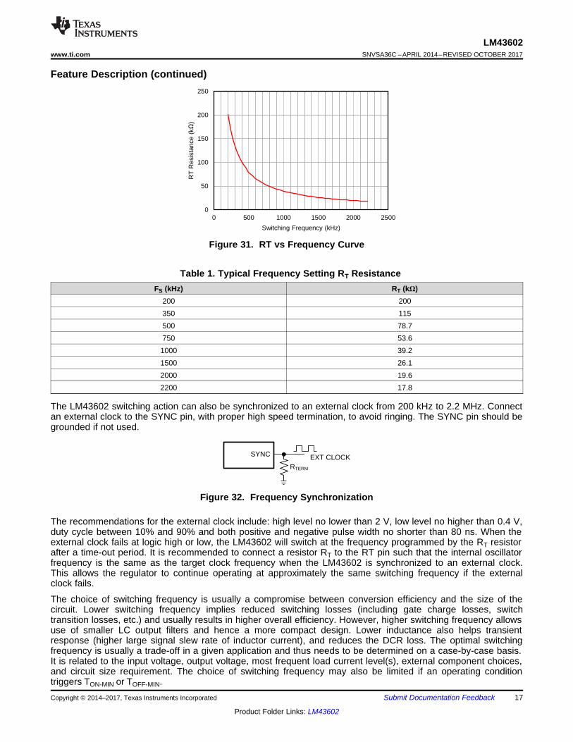
Figure 31. RT vs Frequency Curve
Table 1. Typical Frequency Setting RT ResistanceFS (kHz) RT (kΩ)
200 200350 115500 78.7750 53.61000 39.21500 26.12000 19.62200 17.8
The LM43602 switching action can also be synchronized to an external clock from 200 kHz to 2.2 MHz. Connectan external clock to the SYNC pin, with proper high speed termination, to avoid ringing. The SYNC pin should begrounded if not used.
Figure 32. Frequency Synchronization
The recommendations for the external clock include: high level no lower than 2 V, low level no higher than 0.4 V,duty cycle between 10% and 90% and both positive and negative pulse width no shorter than 80 ns. When theexternal clock fails at logic high or low, the LM43602 will switch at the frequency programmed by the RT resistorafter a time-out period. It is recommended to connect a resistor RT to the RT pin such that the internal oscillatorfrequency is the same as the target clock frequency when the LM43602 is synchronized to an external clock.This allows the regulator to continue operating at approximately the same switching frequency if the externalclock fails.
The choice of switching frequency is usually a compromise between conversion efficiency and the size of thecircuit. Lower switching frequency implies reduced switching losses (including gate charge losses, switchtransition losses, etc.) and usually results in higher overall efficiency. However, higher switching frequency allowsuse of smaller LC output filters and hence a more compact design. Lower inductance also helps transientresponse (higher large signal slew rate of inductor current), and reduces the DCR loss. The optimal switchingfrequency is usually a trade-off in a given application and thus needs to be determined on a case-by-case basis.It is related to the input voltage, output voltage, most frequent load current level(s), external component choices,and circuit size requirement. The choice of switching frequency may also be limited if an operating conditiontriggers TON-MIN or TOFF-MIN.
10000
100000
1000000
5.00 5.20 5.40 5.60 5.80 6.00 6.20 6.40 6.60 6.80 7.00
Fre
quen
cy (
Hz)
VIN (V)
0.1A
0.5A
1A
1.5A
2A
C007
18
LM43602SNVSA36C –APRIL 2014–REVISED OCTOBER 2017 www.ti.com
Product Folder Links: LM43602
Submit Documentation Feedback Copyright © 2014–2017, Texas Instruments Incorporated
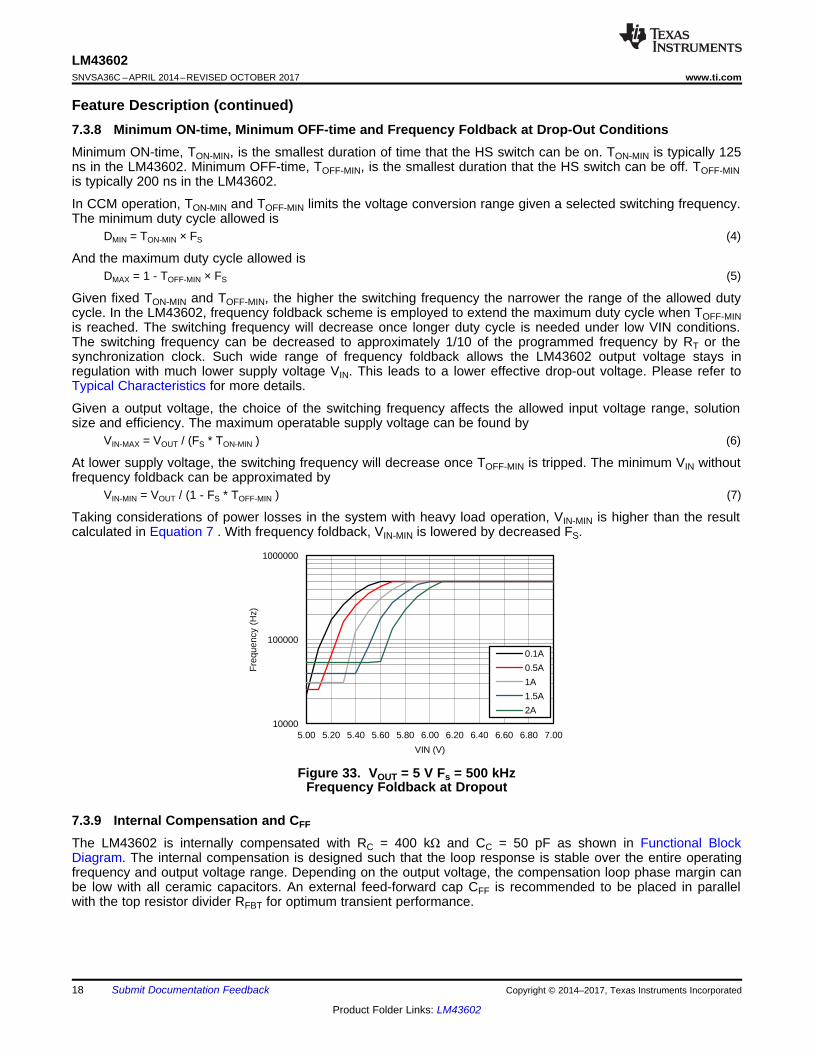
Feature Description (continued)7.3.8 Minimum ON-time, Minimum OFF-time and Frequency Foldback at Drop-Out ConditionsMinimum ON-time, TON-MIN, is the smallest duration of time that the HS switch can be on. TON-MIN is typically 125ns in the LM43602. Minimum OFF-time, TOFF-MIN, is the smallest duration that the HS switch can be off. TOFF-MINis typically 200 ns in the LM43602.
In CCM operation, TON-MIN and TOFF-MIN limits the voltage conversion range given a selected switching frequency.The minimum duty cycle allowed is
DMIN = TON-MIN × FS (4)
And the maximum duty cycle allowed isDMAX = 1 - TOFF-MIN × FS (5)
Given fixed TON-MIN and TOFF-MIN, the higher the switching frequency the narrower the range of the allowed dutycycle. In the LM43602, frequency foldback scheme is employed to extend the maximum duty cycle when TOFF-MINis reached. The switching frequency will decrease once longer duty cycle is needed under low VIN conditions.The switching frequency can be decreased to approximately 1/10 of the programmed frequency by RT or thesynchronization clock. Such wide range of frequency foldback allows the LM43602 output voltage stays inregulation with much lower supply voltage VIN. This leads to a lower effective drop-out voltage. Please refer toTypical Characteristics for more details.
Given a output voltage, the choice of the switching frequency affects the allowed input voltage range, solutionsize and efficiency. The maximum operatable supply voltage can be found by
VIN-MAX = VOUT / (FS * TON-MIN ) (6)
At lower supply voltage, the switching frequency will decrease once TOFF-MIN is tripped. The minimum VIN withoutfrequency foldback can be approximated by
VIN-MIN = VOUT / (1 - FS * TOFF-MIN ) (7)
Taking considerations of power losses in the system with heavy load operation, VIN-MIN is higher than the resultcalculated in Equation 7 . With frequency foldback, VIN-MIN is lowered by decreased FS.
Figure 33. VOUT = 5 V Fs = 500 kHzFrequency Foldback at Dropout
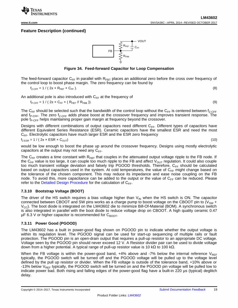
7.3.9 Internal Compensation and CFF
The LM43602 is internally compensated with RC = 400 kΩ and CC = 50 pF as shown in Functional BlockDiagram. The internal compensation is designed such that the loop response is stable over the entire operatingfrequency and output voltage range. Depending on the output voltage, the compensation loop phase margin canbe low with all ceramic capacitors. An external feed-forward cap CFF is recommended to be placed in parallelwith the top resistor divider RFBT for optimum transient performance.
FB
RFBT
RFBB
CFF
VOUT
19
LM43602www.ti.com SNVSA36C –APRIL 2014–REVISED OCTOBER 2017
Product Folder Links: LM43602
Submit Documentation FeedbackCopyright © 2014–2017, Texas Instruments Incorporated
Feature Description (continued)
Figure 34. Feed-forward Capacitor for Loop Compensation
The feed-forward capacitor CFF in parallel with RFBT places an additional zero before the cross over frequency ofthe control loop to boost phase margin. The zero frequency can be found by
fZ-CFF = 1 / ( 2π × RFBT × CFF ). (8)
An additional pole is also introduced with CFF at the frequency offP-CFF = 1 / ( 2π × CFF × ( RFBT // RFBB )). (9)
The CFF should be selected such that the bandwidth of the control loop without the CFF is centered between fZ-CFFand fP-CFF. The zero fZ-CFF adds phase boost at the crossover frequency and improves transient response. Thepole fP-CFF helps maintaining proper gain margin at frequency beyond the crossover.
Designs with different combinations of output capacitors need different CFF. Different types of capacitors havedifferent Equivalent Series Resistance (ESR). Ceramic capacitors have the smallest ESR and need the mostCFF. Electrolytic capacitors have much larger ESR and the ESR zero frequencyfZ-ESR = 1 / ( 2π × ESR × COUT) (10)
would be low enough to boost the phase up around the crossover frequency. Designs using mostly electrolyticcapacitors at the output may not need any CFF.
The CFF creates a time constant with RFBT that couples in the attenuated output voltage ripple to the FB node. Ifthe CFF value is too large, it can couple too much ripple to the FB and affect VOUT regulation. It could also coupletoo much transient voltage deviation and falsely trip PGOOD thresholds. Therefore, CFF should be calculatedbased on output capacitors used in the system. At cold temperatures, the value of CFF might change based onthe tolerance of the chosen component. This may reduce its impedance and ease noise coupling on the FBnode. To avoid this, more capacitance can be added to the output or the value of CFF can be reduced. Pleaserefer to the Detailed Design Procedure for the calculation of CFF.
7.3.10 Bootstrap Voltage (BOOT)The driver of the HS switch requires a bias voltage higher than VIN when the HS switch is ON. The capacitorconnected between CBOOT and SW pins works as a charge pump to boost voltage on the CBOOT pin to (VSW +VCC). The boot diode is integrated on the LM43602 die to minimize Bill-Of-Material (BOM). A synchronous switchis also integrated in parallel with the boot diode to reduce voltage drop on CBOOT. A high quality ceramic 0.47µF 6.3 V or higher capacitor is recommended for CBOOT.
7.3.11 Power Good (PGOOD)The LM43602 has a built in power-good flag shown on PGOOD pin to indicate whether the output voltage iswithin its regulation level. The PGOOD signal can be used for start-up sequencing of multiple rails or faultprotection. The PGOOD pin is an open-drain output that requires a pull-up resistor to an appropriate DC voltage.Voltage seen by the PGOOD pin should never exceed 12 V. A Resistor divider pair can be used to divide voltagedown from a higher potential. A typical range of pull-up resistor value is 10 kΩ to 100 kΩ.
When the FB voltage is within the power-good band, +4% above and -7% below the internal reference VREFtypically, the PGOOD switch will be turned off and the PGOOD voltage will be pulled up to the voltage leveldefined by the pull up resistor or divider. When the FB voltage is outside of the tolerance band, +10% above or-13% below VREF typically, the PGOOD switch will be turned on and the PGOOD pin voltage will be pulled low toindicate power bad. Both rising and falling edges of the power-good flag have a built-in 220 µs (typical) deglitchdelay.
20
LM43602SNVSA36C –APRIL 2014–REVISED OCTOBER 2017 www.ti.com
Product Folder Links: LM43602
Submit Documentation Feedback Copyright © 2014–2017, Texas Instruments Incorporated
Feature Description (continued)7.3.12 Over Current and Short Circuit ProtectionThe LM43602 is protected from over-current conditions by cycle-by-cycle current limiting on both peak and valleyof the inductor current. Hiccup mode will be activated if a fault condition persists to prevent over heating.
High-side MOSFET over-current protection is implemented by the nature of the Peak Current Mode control. TheHS switch current is sensed when the HS is turned on after a set blanking time. The HS switch current iscompared to the output of the Error Amplifier (EA) minus slope compensation every switching cycle. Please referto Functional Block Diagram for more details. The peak current of the HS switch is limited by the maximum EAoutput voltage minus the slope compensation at every switching cycle. The slope compensation magnitude at thepeak current is proportional to the duty cycle.
When the LS switch is turned on, the current going through it is also sensed and monitored. The LS switch willnot be turned OFF at the end of a switching cycle if its current is above the LS current limit ILS-LIMIT. The LSswitch will be kept ON so that inductor current keeps ramping down, until the inductor current ramps below theLS current limit. Then the LS switch will be turned OFF and the HS switch will be turned on after a dead time. Ifthe current of the LS switch is higher than the LS current limit for 32 consecutive cycles and the power-good flagis low, hiccup current protection mode will be activated. In hiccup mode, the regulator will be shutdown and keptoff for 5.5 ms typically before the LM43602 tries to start again. If over-current or short-circuit fault condition stillexist, hiccup will repeat until the fault condition is removed. Hiccup mode reduces power dissipation under severeover-current conditions, prevents over heating and potential damage to the device.
Hiccup is only activated when power-good flag is low. Under non-severe over-current conditions when VOUT hasnot fallen outside of the PGOOD tolerance band, the LM43602 will reduce the switching frequency and keep theinductor current valley clamped at the LS current limit level. This operation mode allows slight over currentoperation during load transients without tripping hiccup. If power-good flag becomes low, hiccup operation willstart after LS current limit is tripped 32 consecutive cycles.
7.3.13 Thermal ShutdownThermal shutdown is a built-in self protection to limit junction temperature and prevent damages due to overheating. Thermal shutdown turns off the device when the junction temperature exceeds 160°C typically toprevent further power dissipation and temperature rise. Junction temperature will reduce after thermal shutdown.The LM43602 will attempt to restart when the junction temperature drops to 150°C.
7.4 Device Functional Modes
7.4.1 Shutdown ModeThe EN pin provides electrical ON and OFF control for the LM43602. When VEN is below 0.4 V, the device is inshutdown mode. Both the internal LDO and the switching regulator are off. In shutdown mode the quiescentcurrent drops to 2.3 µA typically with VIN = 24 V. The LM43602 also employs under voltage lock out protection. IfVCC voltage is below the UVLO level, the output of the regulator will be turned off.
7.4.2 Stand-by ModeThe internal LDO has a lower enable threshold than the regulator. When VEN is above 1.2 V and below theprecision enable falling threshold (1.8 V typically), the internal LDO regulates the VCC voltage at 3.2 V. Theprecision enable circuitry is turned on once VCC is above the UVLO threshold. The switching action and voltageregulation are not enabled unless VEN rises above the precision enable threshold (2.1 V typically).
7.4.3 Active ModeThe LM43602 is in Active Mode when VEN is above the precision enable threshold and VCC is above its UVLOlevel. The simplest way to enable the LM43602 is to connect the EN pin to VIN. This allows self start-up of theLM43602 when the input voltage is in the operation range: 3.5 V to 36 V. Please refer to Enable (EN) and VCC,UVLO and BIAS for details on setting these operating levels.
In Active Mode, depending on the load current, the LM43602 will be in one of four modes:1. Continuous conduction mode (CCM) with fixed switching frequency when load current is above half of the
peak-to-peak inductor current ripple;
1000
10000
100000
1000000
0.001 0.01 0.1 1
Fre
quen
cy
(Hz)
Current (A)
8V 12V 24V 36V
C007
21
LM43602www.ti.com SNVSA36C –APRIL 2014–REVISED OCTOBER 2017
Product Folder Links: LM43602
Submit Documentation FeedbackCopyright © 2014–2017, Texas Instruments Incorporated
Device Functional Modes (continued)2. Discontinuous conduction mode (DCM) with fixed switching frequency when load current is lower than half of
the peak-to-peak inductor current ripple in CCM operation;3. Pulse Frequency Modulation (PFM) when switching frequency is decreased at very light load;4. Fold-back mode when switching frequency is decreased to maintain output regulation at lower supply voltage
VIN.
7.4.4 CCM ModeConstant Current Mode (CCM) operation is employed in the LM43602 when the load current is higher than halfof the peak-to-peak inductor current. In CCM peration, the frequency of operation is fixed unless the theminimum HS switch ON-time (TON_MIN) or OFF-time (TOFF_MIN) is exceeded. Output voltage ripple will be at aminimum in this mode and the maximum output current of 2 A can be supplied by the LM43602.
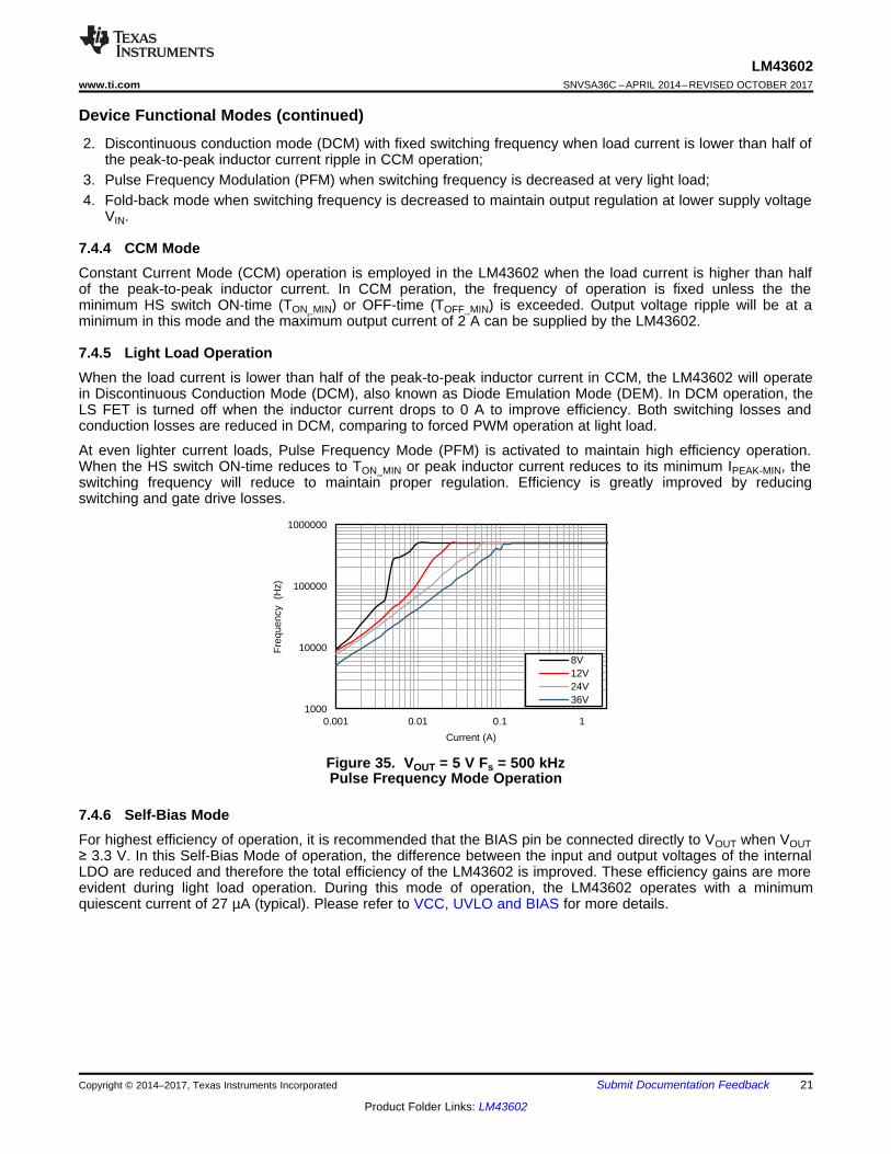
7.4.5 Light Load OperationWhen the load current is lower than half of the peak-to-peak inductor current in CCM, the LM43602 will operatein Discontinuous Conduction Mode (DCM), also known as Diode Emulation Mode (DEM). In DCM operation, theLS FET is turned off when the inductor current drops to 0 A to improve efficiency. Both switching losses andconduction losses are reduced in DCM, comparing to forced PWM operation at light load.
At even lighter current loads, Pulse Frequency Mode (PFM) is activated to maintain high efficiency operation.When the HS switch ON-time reduces to TON_MIN or peak inductor current reduces to its minimum IPEAK-MIN, theswitching frequency will reduce to maintain proper regulation. Efficiency is greatly improved by reducingswitching and gate drive losses.
Figure 35. VOUT = 5 V Fs = 500 kHzPulse Frequency Mode Operation
7.4.6 Self-Bias ModeFor highest efficiency of operation, it is recommended that the BIAS pin be connected directly to VOUT when VOUT≥ 3.3 V. In this Self-Bias Mode of operation, the difference between the input and output voltages of the internalLDO are reduced and therefore the total efficiency of the LM43602 is improved. These efficiency gains are moreevident during light load operation. During this mode of operation, the LM43602 operates with a minimumquiescent current of 27 µA (typical). Please refer to VCC, UVLO and BIAS for more details.
SWVIN
PGND
CBOOT
VCC
BIAS
SYNC
RT
ENABLE
SS/TRK
AGND
FB
LM43602
VIN
COUTCBOOTCIN
CVCC
VOUT
RFBT
RFBB
CFF
L
PGOOD
SWVIN
PGND
CBOOT
VCC
BIAS
SYNC
RT
ENABLE
SS/TRK
AGND
FB
LM43602
VIN
COUTCBOOTCIN
CVCC
VOUT
CBIAS
RFBT
RFBB
CFF
L
PGOOD
22
LM43602SNVSA36C –APRIL 2014–REVISED OCTOBER 2017 www.ti.com
Product Folder Links: LM43602
Submit Documentation Feedback Copyright © 2014–2017, Texas Instruments Incorporated
8 Applications and Implementation
8.1 Application InformationThe LM43602 is a step down DC-to-DC regulator. It is typically used to convert a higher DC voltage to a lowerDC voltage with a maximum output current of 2 A. The following design procedure can be used to selectcomponents for the LM43602. Alternately, the WEBENCH® software may be used to generate complete designs.When generating a design, the WEBENCH® software utilizes iterative design procedure and accessescomprehensive databases of components. Please go to ti.com for more details.
This section presents a simplified discussion of the design process.
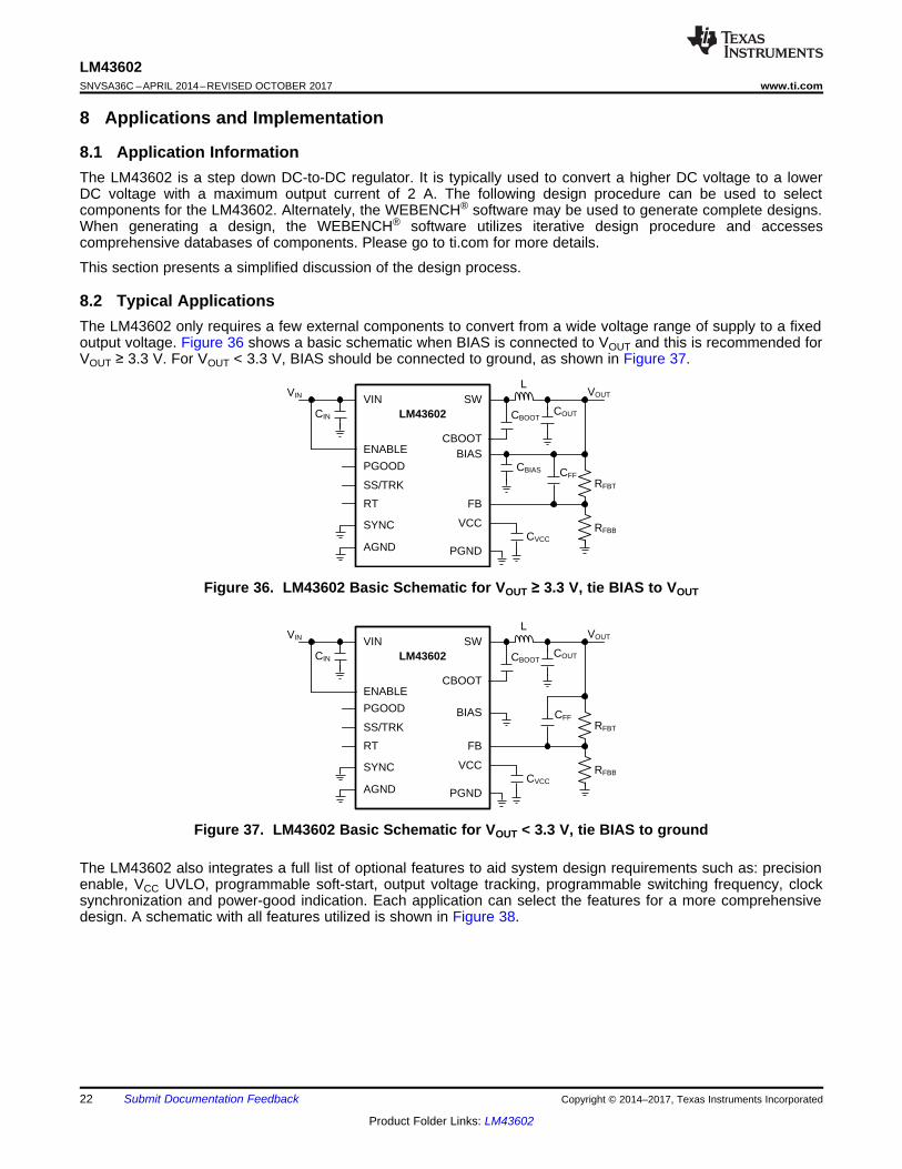
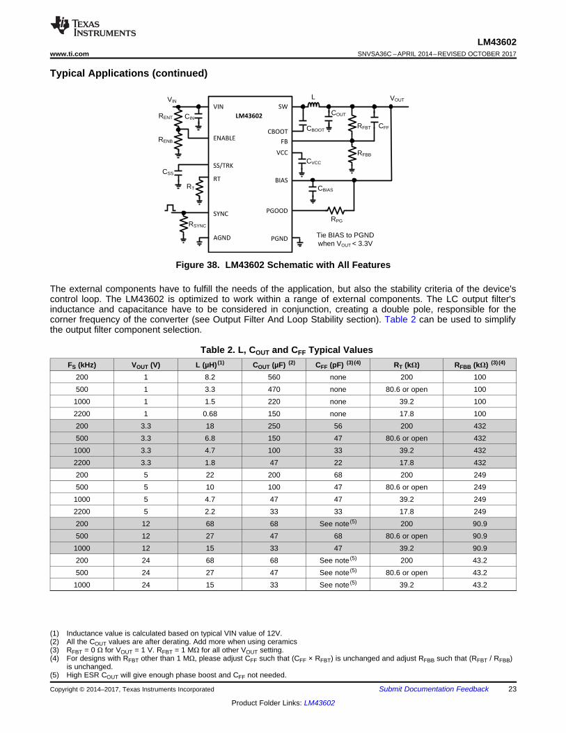
8.2 Typical ApplicationsThe LM43602 only requires a few external components to convert from a wide voltage range of supply to a fixedoutput voltage. Figure 36 shows a basic schematic when BIAS is connected to VOUT and this is recommended forVOUT ≥ 3.3 V. For VOUT < 3.3 V, BIAS should be connected to ground, as shown in Figure 37.
Figure 36. LM43602 Basic Schematic for VOUT ≥ 3.3 V, tie BIAS to VOUT
Figure 37. LM43602 Basic Schematic for VOUT < 3.3 V, tie BIAS to ground
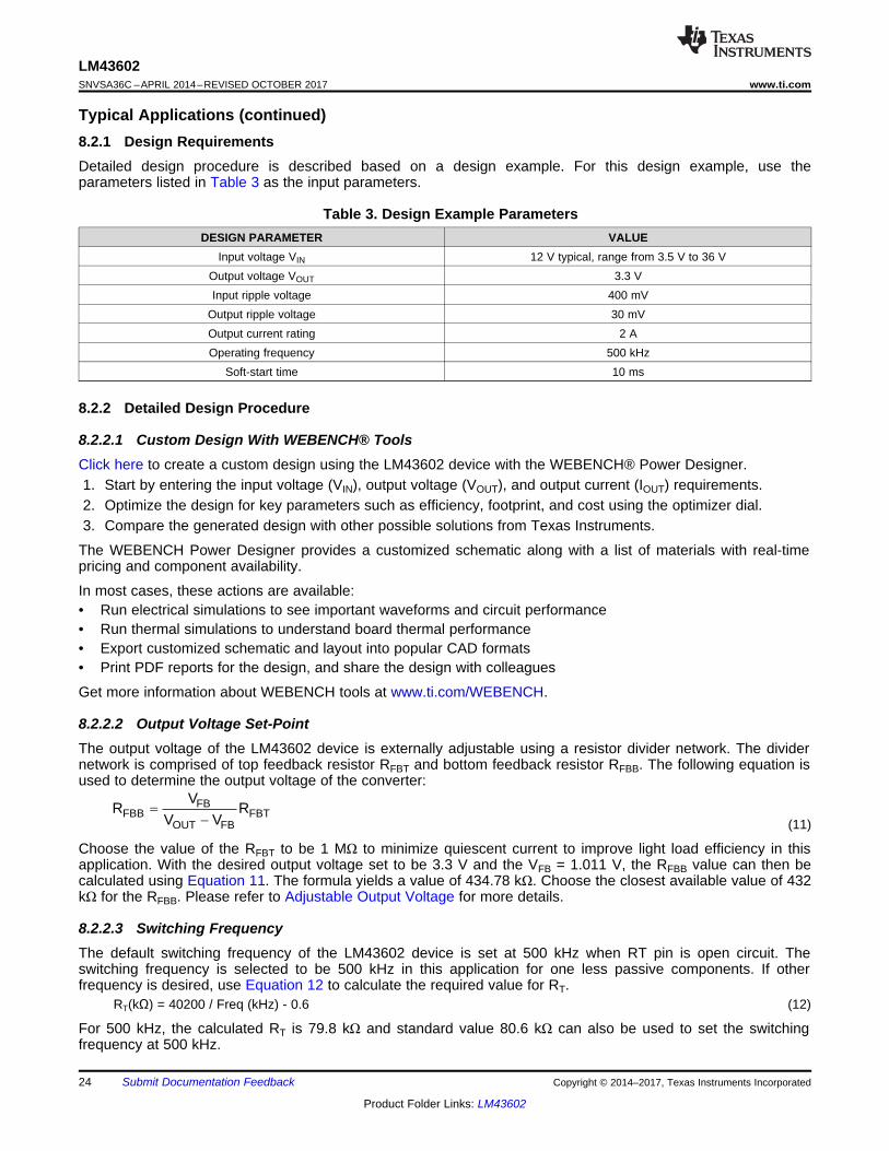
The LM43602 also integrates a full list of optional features to aid system design requirements such as: precisionenable, VCC UVLO, programmable soft-start, output voltage tracking, programmable switching frequency, clocksynchronization and power-good indication. Each application can select the features for a more comprehensivedesign. A schematic with all features utilized is shown in Figure 38.
SWVIN
PGND
CBOOT
VCC
BIAS
SYNC
RT
PGOOD
ENABLE
SS/TRK
AGND
FB
LM43602COUT
CBOOT
CIN
CVCC
CBIAS
RFBT
RFBB
CFF
L
CSS
RT
RSYNC
Tie BIAS to PGND when VOUT < 3.3V
VIN VOUT
RENT
RENB
RPG
23
LM43602www.ti.com SNVSA36C –APRIL 2014–REVISED OCTOBER 2017
Product Folder Links: LM43602
Submit Documentation FeedbackCopyright © 2014–2017, Texas Instruments Incorporated
Typical Applications (continued)
(1) Inductance value is calculated based on typical VIN value of 12V.(2) All the COUT values are after derating. Add more when using ceramics(3) RFBT = 0 Ω for VOUT = 1 V. RFBT = 1 MΩ for all other VOUT setting.(4) For designs with RFBT other than 1 MΩ, please adjust CFF such that (CFF × RFBT) is unchanged and adjust RFBB such that (RFBT / RFBB)
is unchanged.(5) High ESR COUT will give enough phase boost and CFF not needed.
Figure 38. LM43602 Schematic with All Features
The external components have to fulfill the needs of the application, but also the stability criteria of the device'scontrol loop. The LM43602 is optimized to work within a range of external components. The LC output filter'sinductance and capacitance have to be considered in conjunction, creating a double pole, responsible for thecorner frequency of the converter (see Output Filter And Loop Stability section). Table 2 can be used to simplifythe output filter component selection.
Table 2. L, COUT and CFF Typical ValuesFS (kHz) VOUT (V) L (µH) (1) COUT (µF) (2) CFF (pF) (3) (4) RT (kΩ) RFBB (kΩ) (3) (4)
200 1 8.2 560 none 200 100500 1 3.3 470 none 80.6 or open 100
1000 1 1.5 220 none 39.2 1002200 1 0.68 150 none 17.8 100200 3.3 18 250 56 200 432500 3.3 6.8 150 47 80.6 or open 432
1000 3.3 4.7 100 33 39.2 4322200 3.3 1.8 47 22 17.8 432200 5 22 200 68 200 249500 5 10 100 47 80.6 or open 249
1000 5 4.7 47 47 39.2 2492200 5 2.2 33 33 17.8 249200 12 68 68 See note (5) 200 90.9500 12 27 47 68 80.6 or open 90.9
1000 12 15 33 47 39.2 90.9200 24 68 68 See note (5) 200 43.2500 24 27 47 See note (5) 80.6 or open 43.2
1000 24 15 33 See note (5) 39.2 43.2
FBFBB FBT
OUT FB
VR R
V V
24
LM43602SNVSA36C –APRIL 2014–REVISED OCTOBER 2017 www.ti.com
Product Folder Links: LM43602
Submit Documentation Feedback Copyright © 2014–2017, Texas Instruments Incorporated
Typical Applications (continued)8.2.1 Design RequirementsDetailed design procedure is described based on a design example. For this design example, use theparameters listed in Table 3 as the input parameters.
Table 3. Design Example ParametersDESIGN PARAMETER VALUE
Input voltage VIN 12 V typical, range from 3.5 V to 36 VOutput voltage VOUT 3.3 VInput ripple voltage 400 mV
Output ripple voltage 30 mVOutput current rating 2 AOperating frequency 500 kHz
Soft-start time 10 ms
8.2.2 Detailed Design Procedure
8.2.2.1 Custom Design With WEBENCH® ToolsClick here to create a custom design using the LM43602 device with the WEBENCH® Power Designer.1. Start by entering the input voltage (VIN), output voltage (VOUT), and output current (IOUT) requirements.2. Optimize the design for key parameters such as efficiency, footprint, and cost using the optimizer dial.3. Compare the generated design with other possible solutions from Texas Instruments.
The WEBENCH Power Designer provides a customized schematic along with a list of materials with real-timepricing and component availability.
In most cases, these actions are available:• Run electrical simulations to see important waveforms and circuit performance• Run thermal simulations to understand board thermal performance• Export customized schematic and layout into popular CAD formats• Print PDF reports for the design, and share the design with colleagues
Get more information about WEBENCH tools at www.ti.com/WEBENCH.
8.2.2.2 Output Voltage Set-PointThe output voltage of the LM43602 device is externally adjustable using a resistor divider network. The dividernetwork is comprised of top feedback resistor RFBT and bottom feedback resistor RFBB. The following equation isused to determine the output voltage of the converter:
(11)
Choose the value of the RFBT to be 1 MΩ to minimize quiescent current to improve light load efficiency in thisapplication. With the desired output voltage set to be 3.3 V and the VFB = 1.011 V, the RFBB value can then becalculated using Equation 11. The formula yields a value of 434.78 kΩ. Choose the closest available value of 432kΩ for the RFBB. Please refer to Adjustable Output Voltage for more details.
8.2.2.3 Switching FrequencyThe default switching frequency of the LM43602 device is set at 500 kHz when RT pin is open circuit. Theswitching frequency is selected to be 500 kHz in this application for one less passive components. If otherfrequency is desired, use Equation 12 to calculate the required value for RT.
RT(kΩ) = 40200 / Freq (kHz) - 0.6 (12)
For 500 kHz, the calculated RT is 79.8 kΩ and standard value 80.6 kΩ can also be used to set the switchingfrequency at 500 kHz.
L
OUT
ir
I
'
u ud d
u u u u
IN OUT IN OUT
S L MAX S L MAX
(V V ) D (V V ) DL
0.4 F I 0.2 F I
u'
u
IN OUTL
S
(V V ) Di
L F
25
LM43602www.ti.com SNVSA36C –APRIL 2014–REVISED OCTOBER 2017
Product Folder Links: LM43602
Submit Documentation FeedbackCopyright © 2014–2017, Texas Instruments Incorporated
8.2.2.4 Input CapacitorsThe LM43602 device requires high frequency input decoupling capacitor(s) and a bulk input capacitor, dependingon the application. The typical recommended value for the high frequency decoupling capacitor is 4.7 µF to 10µF. A high-quality ceramic type X5R or X7R with sufficiency voltage rating is recommended. The voltage ratingmust be greater than the maximum input voltage. To compensate the derating of ceramic capactors, a voltagerating of twice the maximum input voltage is recommended. Additionally, some bulk capacitance can be required,especially if the LM43602 circuit is not located within approximately 5 cm from the input voltage source. Thiscapacitor is used to provide damping to the voltage spiking due to the lead inductance of the cable or trace. Thevalue for this capacitor is not critical but must be rated to handle the maximum input voltage including ripple. Forthis design, a 10 µF, X7R dielectric capacitor rated for 100 V is used for the input decoupling capacitor. Theequivalent series resistance (ESR) is approximately 3 mΩ, and the current-rating is 3 A. Include a capacitor witha value of 0.1 µF for high-frequency filtering and place it as close as possible to the device pins.
NOTEDC Bias effect: High capacitance ceramic capacitors have a DC Bias effect, which willhave a strong influence on the final effective capacitance. Therefore the right capacitorvalue has to be chosen carefully. Package size and voltage rating in combination withdielectric material are responsible for differences between the rated capacitor value andthe effective capacitance.
8.2.2.5 Inductor SelectionThe first criterion for selecting an output inductor is the inductance itself. In most buck converters, this value isbased on the desired peak-to-peak ripple current, ΔiL, that flows in the inductor along with the DC load current.As with switching frequency, the selection of the inductor is a tradeoff between size and cost. Higher inductancegives lower ripple current and hence lower output voltage ripple with the same output capacitors. Lowerinductance could result in smaller, less expensive component. An inductance that gives a ripple current of 20% to40% of the 2 A at the typical supply voltage is a good starting point. ΔIL = (1/5 to 2/5) x IOUT. The peak-to-peakinductor current ripple can be found by Equation 13 and the range of inductance can be found by Equation 14with the typical input voltage used as VIN.
(13)
(14)
D is the duty cycle of the converter which in a buck converter can be approximated as D = VIN/VOUT, assumingno loss power conversion. By calculating in terms of amperes, volts, and megahertz, the inductance value willcome out in micro henries. The inductor ripple current ratio is defined by:
(15)
The second criterion is the inductor saturation current rating. The inductor should be rated to handle themaximum load current plus the ripple current:
IL-PEAK = ILOAD-MAX + ΔiL/ 2 (16)
The LM43602 has both valley current limit and peak current limit. During an instantaneous short, the peakinductor current can be high due to a momentary increase in duty cycle. The inductor current rating should behigher than the HS current limit. It is advised to select an inductor with a larger core saturation margin andpreferably a softer roll off of the inductance value over load current.
c u
uS OUT
D 1ESR ( 0.5)
F C r
ª º§ ·
c c! u u u « »¨ ¸¨ ¸u u' « »© ¹¬ ¼
2
OUTS OUT OUT
1 rC (1 D ) D (1 r)
(F r V / I ) 12
26
LM43602SNVSA36C –APRIL 2014–REVISED OCTOBER 2017 www.ti.com
Product Folder Links: LM43602
Submit Documentation Feedback Copyright © 2014–2017, Texas Instruments Incorporated
In general, it is preferable to choose lower inductance in switching power supplies, because it usuallycorresponds to faster transient response, smaller DCR, and reduced size for more compact designs. But too lowof an inductance can generate too large of an inductor current ripple such that over current protection at the fullload could be falsely triggered. It also generates more conduction loss, since the RMS current is slightly higherrelative that with lower current ripple at the same DC current. Larger inductor current ripple also implies largeroutput voltage ripple with the same output capacitors. With peak current mode control, it is not recommended tohave too small of an inductor current ripple. A larger peak current ripple improves the comparator signal to noiseratio.
Once the inductance is determined, the type of inductor must be selected. Ferrite designs have very low corelosses and are preferred at high switching frequencies, so design goals can concentrate on copper loss andpreventing saturation. Ferrite core material saturates hard, which means that inductance collapses abruptly whenthe peak design current is exceeded. The ‘hard’ saturation results in an abrupt increase in inductor ripple currentand consequent output voltage ripple. Do not allow the core to saturate!
For the design example, a standard 6.8 μH inductor from Wurth, Coiltronics, or Vishay can be used for the 3.3 Voutput with plenty of current rating margin.
8.2.2.6 Output Capacitor SelectionThe device is designed to be used with a wide variety of LC filters. It is generally desired to use as little outputcapacitance as possible to keep cost and size down. The output capacitor (s), COUT, should be chosen withcare since it directly affects the steady state output voltage ripple, loop stability and the voltage over/undershootduring load current transients.
The output voltage ripple is essentially composed of two parts. One is caused by the inductor current ripple goingthrough the Equivalent Series Resistance (ESR) of the output capacitors:
ΔVOUT-ESR =ΔiL×ESR (17)
The other is caused by the inductor current ripple charging and discharging the output capacitors:ΔVOUT-C =ΔiL/ ( 8 × FS × COUT ) (18)
The two components in the voltage ripple are not in phase, so the actual peak-to-peak ripple is smaller than thesum of the two peaks.
Output capacitance is usually limited by transient performance specifications if the system requires tight voltageregulation in the presence of large current steps and fast slew rates. When a fast large load transient happens,output capacitors provide the required charge before the inductor current can slew to the appropriate level. Theinitial output voltage step is equal to the load current step multiplied by the ESR. VOUT continues to droop untilthe control loop response increases or decreases the inductor current to supply the load. To maintain a smallover- or undershoot during a transient, small ESR and large capacitance are desired. But these also come withhigher cost and size. Thus, the motivation is to seek a fast control loop response to reduce the output voltagedeviation.
For a given input and output requirement, the following inequality gives an approximation for an absoluteminimum output cap required:
(19)
Along with this for the same requirement, the max ESR should be calculated as per the following inequality
(20)
where
r = Ripple ratio of the inductor ripple current (ΔIL / IOUT)
ΔVOUT = Target output voltage undershoot
D’ = 1 – Duty cycle
FS = Switching Frequency
SS SSC SSC I t u
uS u
FFx FBT FBT FBB
1 1C
2 f R (R / /R )
ux
OUT OUT
4.35f
V C
27
LM43602www.ti.com SNVSA36C –APRIL 2014–REVISED OCTOBER 2017
Product Folder Links: LM43602
Submit Documentation FeedbackCopyright © 2014–2017, Texas Instruments Incorporated
IOUT = Load Current
A general guide line for COUT range is that COUT should be larger than the minimum required output capacitancecalculated by Equation 19, and smaller than 10 times the minimum required output capacitance or 1 mF. Inapplications with VOUT less than 3.3 V, it is critical that low ESR output capacitors are selected. This will limitpotential output voltage overshoots as the input voltage falls below the device normal operating range. Tooptimize the transient behavior a feed-forward capacitor could be added in parallel with the upper feedbackresistor. For this design example, three 47 µF,10 V, X7R ceramic capacitors are used in parallel.
8.2.2.7 Feed-Forward CapacitorThe LM43602 is internally compensated and the internal R-C values are 400 kΩ and 50 pF respectively.Depending on the VOUT and frequency FS, if the output capacitor COUT is dominated by low ESR (ceramic types)capacitors, it could result in low phase margin. To improve the phase boost an external feedforward capacitorCFF can be added in parallel with RFBT. CFF is chosen such that phase margin is boosted at the crossoverfrequency without CFF. A simple estimation for the crossover frequency without CFF (fx) is shown in Equation 21,assuming COUT has very small ESR.
(21)
The following equation for CFF was tested:
(22)
This equation indicates that the crossover frequency is geometrically centered on the zero and pole frequenciescaused by the CFF capacitor.
For designs with higher ESR, CFF is not neeed when COUT has very high ESR and CFF calculated fromEquation 22 should be reduced with medium ESR. Table 2 can be used as a quick starting point.
For the application in this design example, a 100 pF COG capacitor is selected.
8.2.2.8 Bootstrap CapacitorsEvery LM43602 design requires a bootstrap capacitor, CBOOT. The recommended bootstrap capacitor is 0.47 μFand rated at 6.3 V or higher. The bootstrap capacitor is located between the SW pin and the CBOOT pin. Thebootstrap capacitor must be a high-quality ceramic type with X7R or X5R grade dielectric for temperaturestability.
8.2.2.9 VCC CapacitorThe VCC pin is the output of an internal LDO for LM43602. The input for this LDO comes from either VIN orBIAS (please refer to Functional Block Diagram for LM43602). To insure stability of the part, place a minimum of2.2 µF, 10 V capacitor from this pin to ground.
8.2.2.10 BIAS CapacitorsFor an output voltage of 3.3 V and greater, the BIAS pin can be connected to the output in order to increase lightload efficiency. This pin is an input for the VCC LDO. When BIAS is not connected, the input for the VCC LDOwill be internally connected into VIN. Since this is an LDO, the voltage differences between the input and outputwill affect the efficiency of the LDO. If necessary, a capacitor with a value of 1 μF can be added close to theBIAS pin as an input capacitor for the LDO.
8.2.2.11 Soft-Start CapacitorsThe user can left the SS/TRK pin floating and the LM43602 will implement a soft start time of 4.1 ms typically. Inorder to use an external soft start capacitor, the capacitor should be sized such that the soft start time will belonger than 4.1 ms. Use the following equation in order to calculate the soft start capacitor value:
(23)
Where,
28
LM43602SNVSA36C –APRIL 2014–REVISED OCTOBER 2017 www.ti.com
Product Folder Links: LM43602
Submit Documentation Feedback Copyright © 2014–2017, Texas Instruments Incorporated
CSS = Soft start capacitor value (µF)
ISS = Soft start charging current (µA)
tSS = Desired soft start time (s)
For the desired soft start time of 10 ms and soft start charging current of 2.0 µA, the equation above yield a softstart capacitor value of 0.020 µF.
8.2.2.12 Under Voltage Lockout Set-PointThe undervoltage lockout (UVLO) is adjusted using the external voltage divider network of RENT and RENB. RENTis connected between VIN and the EN pin of the LM43602 device. RENB is connected between the EN pin andthe GND pin. The UVLO has two thresholds, one for power up when the input voltage is rising and one for powerdown or brown outs when the input voltage is falling. The following equation can be used to determine the VIN(UVLO) level.
VIN-UVLO-RISING = VENH × (RENB + RENT) / RENB (24)
The EN rising threshold (VENH) for LM43602 is set to be 2.2 V (typical). Choose the value of RENB to be 1 MΩ tominimize input current from the supply. If the desired VIN UVLO level is at 5.0 V, then the value of RENT can becalculated using the equation below:
RENT = (VIN-UVLO-RISING / VENH -1) × RENB (25)
The above equation yields a value of 1.27 MΩ. The resulting falling UVLO threshold, equals 4.3 V, can becalculated by below equation, where EN falling threshold (VENL) is 1.9 V (typical).
VIN-UVLO-FALLING = VENL × (RENB + RENT) / RENB (26)
8.2.2.13 PGOODA typical pull-up resistor value is 10 kΩ to 100 kΩ from PGOOD pin to a voltage no higher than 12 V. If it isdesired to pull up PGOOD pin to a voltage higher than 12 V, a resistor can be added from PGOOD pin to groundto divide the voltage seen by the PGOOD pin to a value no higher than 12 V.
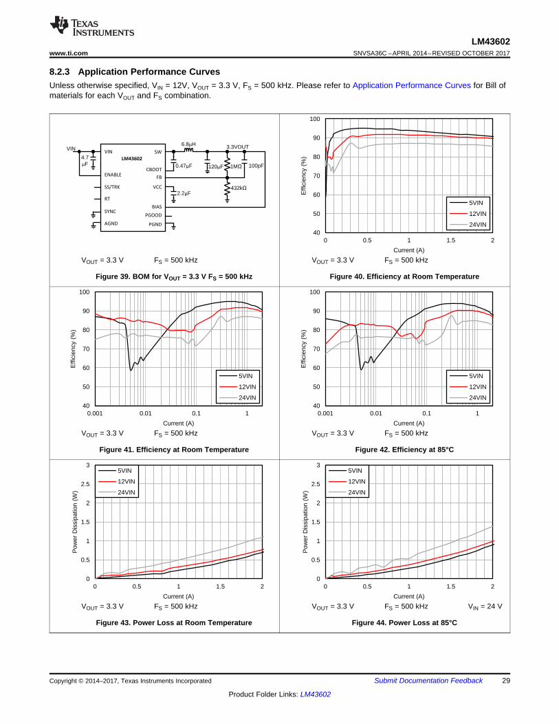
0
0.5
1
1.5
2
2.5
3
0 0.5 1 1.5 2
Pow
er D
issi
patio
n (W
)
Current (A)
5VIN
12VIN
24VIN
C001
0
0.5
1
1.5
2
2.5
3
0 0.5 1 1.5 2
Pow
er D
issi
patio
n (W
)
Current (A)
5VIN
12VIN
24VIN
C001
40
50
60
70
80
90
100
0.001 0.01 0.1 1
Effi
cien
cy (
%)
Current (A)
5VIN
12VIN
24VIN
C001
40
50
60
70
80
90
100
0.001 0.01 0.1 1
Effi
cien
cy (
%)
Current (A)
5VIN
12VIN
24VIN
C001
C001
SWVIN
PGND
CBOOT
VCC
BIASSYNC
RT
PGOOD
ENABLE
SS/TRK
AGND
FB
LM43602
VIN
120µF0.47µF
4.7µF
2.2µF
3.3VOUT
1M
432k
100pF
6.8µH
40
50
60
70
80
90
100
0 0.5 1 1.5 2
Effi
cien
cy (
%)
Current (A)
5VIN
12VIN
24VIN
C001
29
LM43602www.ti.com SNVSA36C –APRIL 2014–REVISED OCTOBER 2017
Product Folder Links: LM43602
Submit Documentation FeedbackCopyright © 2014–2017, Texas Instruments Incorporated
8.2.3 Application Performance CurvesUnless otherwise specified, VIN = 12V, VOUT = 3.3 V, FS = 500 kHz. Please refer to Application Performance Curves for Bill ofmaterials for each VOUT and FS combination.
VOUT = 3.3 V FS = 500 kHz
Figure 39. BOM for VOUT = 3.3 V FS = 500 kHz
VOUT = 3.3 V FS = 500 kHz
Figure 40. Efficiency at Room Temperature
VOUT = 3.3 V FS = 500 kHz
Figure 41. Efficiency at Room Temperature
VOUT = 3.3 V FS = 500 kHz
Figure 42. Efficiency at 85°C
VOUT = 3.3 V FS = 500 kHz
Figure 43. Power Loss at Room Temperature
VOUT = 3.3 V FS = 500 kHz VIN = 24 V
Figure 44. Power Loss at 85°C
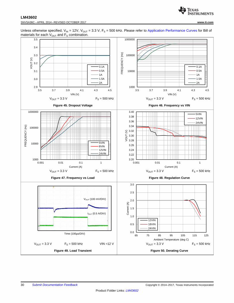
Time (100µs/DIV)
VOUT (100 mV/DIV)
IOUT (0.5 A/DIV)
0.0
0.5
1.0
1.5
2.0
2.5
3.0
65 75 85 95 105 115 125
Cur
rent
(A
)
Ambient Temperature (deg C)
12VIN
18VIN
24VIN
C007
1000
10000
100000
1000000
0.001 0.01 0.1 1
FR
EQ
UE
NC
Y (
Hz)
Current (A)
5VIN 8VIN 12VIN 24VIN
C007
3.20
3.22
3.24
3.26
3.28
3.30
3.32
3.34
3.36
3.38
3.40
0.001 0.01 0.1 1
VO
UT
(V
)
Current (A)
5VIN
12VIN
24VIN
C001
2.9
3.0
3.1
3.2
3.3
3.4
3.5
3.5 3.7 3.9 4.1 4.3 4.5
VO
UT
(V
)
VIN (V)
0.1A
0.5A
1A
1.5A
2A
C007
1000
10000
100000
1000000
3.5 3.7 3.9 4.1 4.3 4.5
FR
EQ
UE
NC
Y (
Hz)
VIN (V)
0.1A
0.5A
1A
1.5A
2A
C007
30
LM43602SNVSA36C –APRIL 2014–REVISED OCTOBER 2017 www.ti.com
Product Folder Links: LM43602
Submit Documentation Feedback Copyright © 2014–2017, Texas Instruments Incorporated
Unless otherwise specified, VIN = 12V, VOUT = 3.3 V, FS = 500 kHz. Please refer to Application Performance Curves for Bill ofmaterials for each VOUT and FS combination.
VOUT = 3.3 V FS = 500 kHz
Figure 45. Dropout Voltage
VOUT = 3.3 V FS = 500 kHz
Figure 46. Frequency vs VIN
VOUT = 3.3 V FS = 500 kHz
Figure 47. Frequency vs Load
VOUT = 3.3 V FS = 500 kHz
Figure 48. Regulation Curve
VOUT = 3.3 V FS = 500 kHz VIN =12 V
Figure 49. Load Transient
VOUT = 3.3 V FS = 500 kHz
Figure 50. Derating Curve
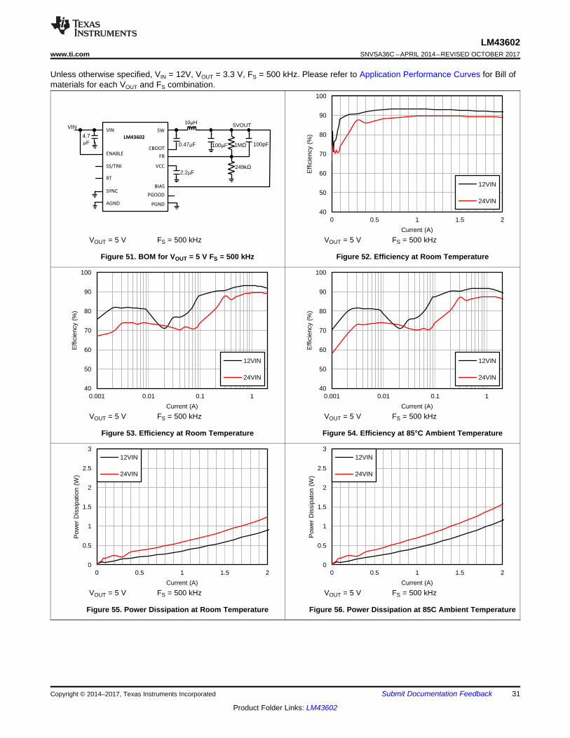
0
0.5
1
1.5
2
2.5
3
0 0.5 1 1.5 2
Pow
er D
issi
patio
n (W
)
Current (A)
12VIN
24VIN
C001
0
0.5
1
1.5
2
2.5
3
0 0.5 1 1.5 2
Pow
er D
issi
pato
n (W
)
Current (A)
12VIN
24VIN
C001
40
50
60
70
80
90
100
0.001 0.01 0.1 1
Effi
cien
cy (
%)
Current (A)
12VIN
24VIN
C001
40
50
60
70
80
90
100
0.001 0.01 0.1 1
Effi
cien
cy (
%)
Current (A)
12VIN
24VIN
C001
C001
SWVIN
PGND
CBOOT
VCC
BIASSYNC
RT
PGOOD
ENABLE
SS/TRK
AGND
FB
LM43602
VIN
100µF0.47µF
4.7µF
2.2µF
5VOUT
1M
249k
100pF
10µH
40
50
60
70
80
90
100
0 0.5 1 1.5 2
Effi
cien
cy (
%)
Current (A)
12VIN
24VIN
C001
31
LM43602www.ti.com SNVSA36C –APRIL 2014–REVISED OCTOBER 2017
Product Folder Links: LM43602
Submit Documentation FeedbackCopyright © 2014–2017, Texas Instruments Incorporated
Unless otherwise specified, VIN = 12V, VOUT = 3.3 V, FS = 500 kHz. Please refer to Application Performance Curves for Bill ofmaterials for each VOUT and FS combination.
VOUT = 5 V FS = 500 kHz
Figure 51. BOM for VOUT = 5 V FS = 500 kHz
VOUT = 5 V FS = 500 kHz
Figure 52. Efficiency at Room Temperature
VOUT = 5 V FS = 500 kHz
Figure 53. Efficiency at Room Temperature
VOUT = 5 V FS = 500 kHz
Figure 54. Efficiency at 85°C Ambient Temperature
VOUT = 5 V FS = 500 kHz
Figure 55. Power Dissipation at Room Temperature
VOUT = 5 V FS = 500 kHz
Figure 56. Power Dissipation at 85C Ambient Temperature
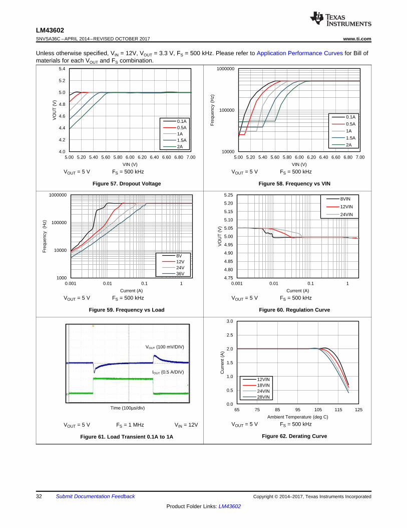
Time (100µs/div)
VOUT (100 mV/DIV)
IOUT (0.5 A/DIV)
0.0
0.5
1.0
1.5
2.0
2.5
3.0
65 75 85 95 105 115 125
Cur
rent
(A
)
Ambient Temperature (deg C)
12VIN 18VIN 24VIN 28VIN
C007
1000
10000
100000
1000000
0.001 0.01 0.1 1
Fre
quen
cy
(Hz)
Current (A)
8V 12V 24V 36V
C007
4.75
4.80
4.85
4.90
4.95
5.00
5.05
5.10
5.15
5.20
5.25
0.001 0.01 0.1 1
VO
UT
(V
)
Current (A)
8VIN
12VIN
24VIN
C004
4.0
4.2
4.4
4.6
4.8
5.0
5.2
5.4
5.00 5.20 5.40 5.60 5.80 6.00 6.20 6.40 6.60 6.80 7.00
VO
UT
(V
)
VIN (V)
0.1A 0.5A 1A 1.5A 2A
C007
10000
100000
1000000
5.00 5.20 5.40 5.60 5.80 6.00 6.20 6.40 6.60 6.80 7.00
Fre
quen
cy (
Hz)
VIN (V)
0.1A
0.5A
1A
1.5A
2A
C007
32
LM43602SNVSA36C –APRIL 2014–REVISED OCTOBER 2017 www.ti.com
Product Folder Links: LM43602
Submit Documentation Feedback Copyright © 2014–2017, Texas Instruments Incorporated
Unless otherwise specified, VIN = 12V, VOUT = 3.3 V, FS = 500 kHz. Please refer to Application Performance Curves for Bill ofmaterials for each VOUT and FS combination.
VOUT = 5 V FS = 500 kHz
Figure 57. Dropout Voltage
VOUT = 5 V FS = 500 kHz
Figure 58. Frequency vs VIN
VOUT = 5 V FS = 500 kHz
Figure 59. Frequency vs Load
VOUT = 5 V FS = 500 kHz
Figure 60. Regulation Curve
VOUT = 5 V FS = 1 MHz VIN = 12V
Figure 61. Load Transient 0.1A to 1A
VOUT = 5 V FS = 500 kHz
Figure 62. Derating Curve
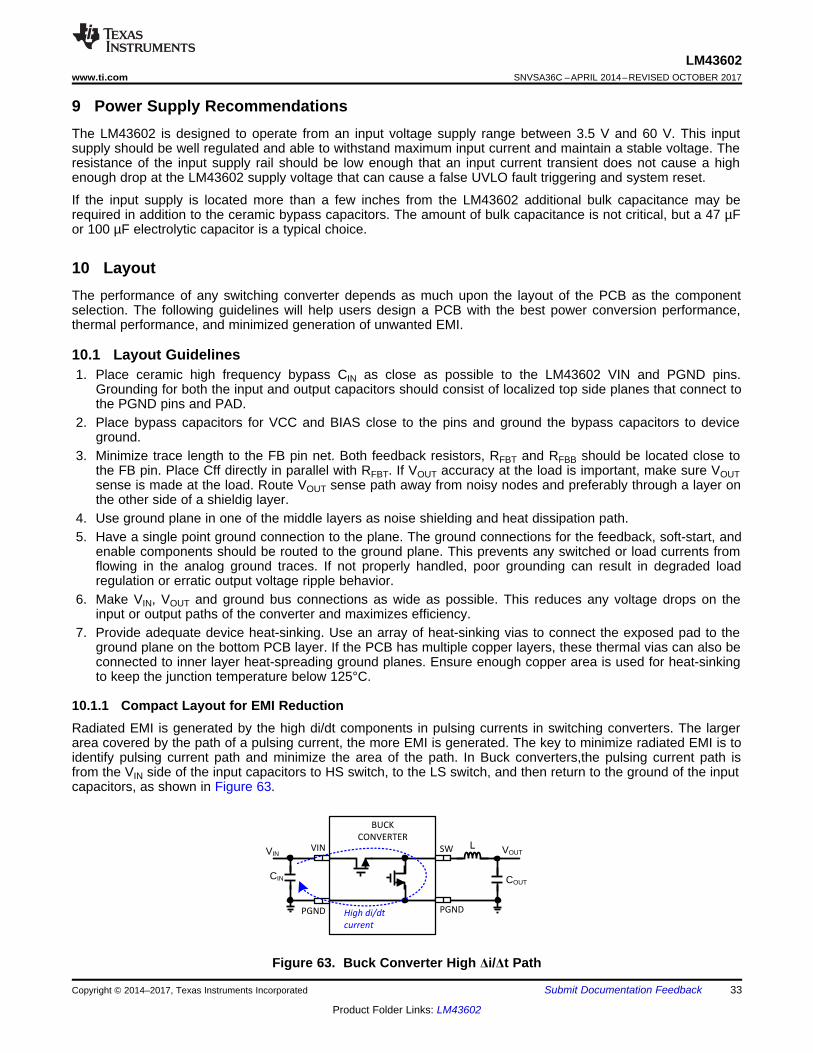
SWVIN
PGNDPGND
CIN
VIN
COUT
VOUTL
High di/dt
current
BUCK
CONVERTER
33
LM43602www.ti.com SNVSA36C –APRIL 2014–REVISED OCTOBER 2017
Product Folder Links: LM43602
Submit Documentation FeedbackCopyright © 2014–2017, Texas Instruments Incorporated
9 Power Supply RecommendationsThe LM43602 is designed to operate from an input voltage supply range between 3.5 V and 60 V. This inputsupply should be well regulated and able to withstand maximum input current and maintain a stable voltage. Theresistance of the input supply rail should be low enough that an input current transient does not cause a highenough drop at the LM43602 supply voltage that can cause a false UVLO fault triggering and system reset.
If the input supply is located more than a few inches from the LM43602 additional bulk capacitance may berequired in addition to the ceramic bypass capacitors. The amount of bulk capacitance is not critical, but a 47 µFor 100 µF electrolytic capacitor is a typical choice.
10 LayoutThe performance of any switching converter depends as much upon the layout of the PCB as the componentselection. The following guidelines will help users design a PCB with the best power conversion performance,thermal performance, and minimized generation of unwanted EMI.
10.1 Layout Guidelines1. Place ceramic high frequency bypass CIN as close as possible to the LM43602 VIN and PGND pins.
Grounding for both the input and output capacitors should consist of localized top side planes that connect tothe PGND pins and PAD.
2. Place bypass capacitors for VCC and BIAS close to the pins and ground the bypass capacitors to deviceground.
3. Minimize trace length to the FB pin net. Both feedback resistors, RFBT and RFBB should be located close tothe FB pin. Place Cff directly in parallel with RFBT. If VOUT accuracy at the load is important, make sure VOUTsense is made at the load. Route VOUT sense path away from noisy nodes and preferably through a layer onthe other side of a shieldig layer.
4. Use ground plane in one of the middle layers as noise shielding and heat dissipation path.5. Have a single point ground connection to the plane. The ground connections for the feedback, soft-start, and
enable components should be routed to the ground plane. This prevents any switched or load currents fromflowing in the analog ground traces. If not properly handled, poor grounding can result in degraded loadregulation or erratic output voltage ripple behavior.
6. Make VIN, VOUT and ground bus connections as wide as possible. This reduces any voltage drops on theinput or output paths of the converter and maximizes efficiency.
7. Provide adequate device heat-sinking. Use an array of heat-sinking vias to connect the exposed pad to theground plane on the bottom PCB layer. If the PCB has multiple copper layers, these thermal vias can also beconnected to inner layer heat-spreading ground planes. Ensure enough copper area is used for heat-sinkingto keep the junction temperature below 125°C.
10.1.1 Compact Layout for EMI ReductionRadiated EMI is generated by the high di/dt components in pulsing currents in switching converters. The largerarea covered by the path of a pulsing current, the more EMI is generated. The key to minimize radiated EMI is toidentify pulsing current path and minimize the area of the path. In Buck converters,the pulsing current path isfrom the VIN side of the input capacitors to HS switch, to the LS switch, and then return to the ground of the inputcapacitors, as shown in Figure 63.
Figure 63. Buck Converter High Δi/Δt Path
34
LM43602SNVSA36C –APRIL 2014–REVISED OCTOBER 2017 www.ti.com
Product Folder Links: LM43602
Submit Documentation Feedback Copyright © 2014–2017, Texas Instruments Incorporated
Layout Guidelines (continued)High frequency ceramic bypass capacitors at the input side provide primary path for the high di/dt components ofthe pulsing current. Placing ceramic bypass capacitor(s) as close as possible to the VIN and PGND pins is thekey to EMI reduction.
The SW pin connecting to the inductor should be as short as possible, and just wide enough to carry the loadcurrent without excessive heating. Short, thick traces or copper pours (shapes) should be used for high currentcondution path to minimize parasitic resistance. The output capacitors should be place close to the VOUT end ofthe inductor and closely grounded to PGND pin and exposed PAD.
The bypass capacitors on VCC and BIAS pins should be placed as close as possible to the pins respectively andclosely grounded to PGND and the exposed PAD.
10.1.2 Ground Plane and Thermal ConsiderationsIt is recommended to use one of the middle layers as a solid ground plane. Ground plane provides shielding forsensitive circuits and traces. It also provides a quiet reference potential for the control circuitry. The AGND andPGND pins should be connected to the ground plane using vias right next to the bypass capacitors. PGND pinsare connected to the source of the internal LS switch. They should be connected directly to the grounds of theinput and output capacitors. The PGND net contains noise at switching frequency and may bounce due to loadvariations. PGND trace, as well as PVIN and SW traces, should be constrained to one side of the ground plane.The other side of the ground plane contains much less noise and should be used for sensitive routes.
It is recommended to provide adequate device heat sinking by utilizing the PAD of the IC as the primary thermalpath. Use a minimum 4 by 4 array of 10 mil thermal vias to connect the PAD to the system ground plane heatsink. The vias should be evenly distributed under the PAD. Use as much copper as possible for system groundplane on the top and bottom layers for the best heat dissipation. Use a four-layer board with the copper thicknessfor the four layers, starting from the top one, 2 oz / 1 oz / 1 oz / 2 oz. Four layer boards with enough copperthickness provides low current conduction impedance, proper shielding and lower thermal resistance.
The thermal characteristics of the LM46002 are specified using the parameter RθJA, which characterize thejunction temperature of the silicon to the ambient temperature in a specific system. Although the value of θJA isdependant on many variables, it still can be used to approximate the operating junction temperature of thedevice. To obtain an estimate of the device junction temperature, one may use the following relationship:
TJ = PD× θJA + TA (27)
where
TJ = Junction temperature in °C
PD = VIN × IIN × (1 − Efficiency) − 1.1 x IOUT x DCR
DCR = Inductor DC parasitic resistance in Ω
θJA = Junction-to-ambient thermal resistance of the device in °C/W
TA = Ambient temperature in °C.
The maximum operating junction temperature of the LM43602 is 125°C. θJA is highly related to PCB size andlayout, as well as enviromental factors such as heat sinking and air flow. Figure 64 shows measured results ofRθJA with different copper area on a 2-layer board and a 4-layer board.
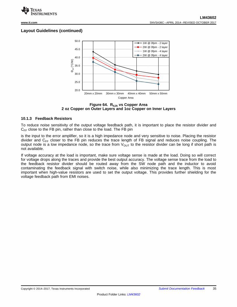
20.0
25.0
30.0
35.0
40.0
45.0
50.0
20mm x 20mm 30mm x 30mm 40mm x 40mm 50mm x 50mm
,JA
(C
/W)
Copper Area
1W @ 0fpm - 2 layer
2W @ 0fpm - 2 layer
1W @ 0fpm - 4 layer
2W @ 0fpm - 4 layer
C007
35
LM43602www.ti.com SNVSA36C –APRIL 2014–REVISED OCTOBER 2017
Product Folder Links: LM43602
Submit Documentation FeedbackCopyright © 2014–2017, Texas Instruments Incorporated
Layout Guidelines (continued)
Figure 64. RθJA vs Copper Area2 oz Copper on Outer Layers and 1oz Copper on Inner Layers
10.1.3 Feedback ResistorsTo reduce noise sensitivity of the output voltage feedback path, it is important to place the resistor divider andCFF close to the FB pin, rather than close to the load. The FB pin
is the input to the error amplifier, so it is a high impedance node and very sensitive to noise. Placing the resistordivider and CFF closer to the FB pin reduces the trace length of FB signal and reduces noise coupling. Theoutput node is a low impedance node, so the trace from VOUT to the resistor divider can be long if short path isnot available.
If voltage accuracy at the load is important, make sure voltage sense is made at the load. Doing so will correctfor voltage drops along the traces and provide the best output accuracy. The voltage sense trace from the load tothe feedback resistor divider should be routed away from the SW node path and the inductor to avoidcontaminating the feedback signal with switch noise, while also minimizing the trace length. This is mostimportant when high-value resistors are used to set the output voltage. This provides further shielding for thevoltage feedback path from EMI noises.
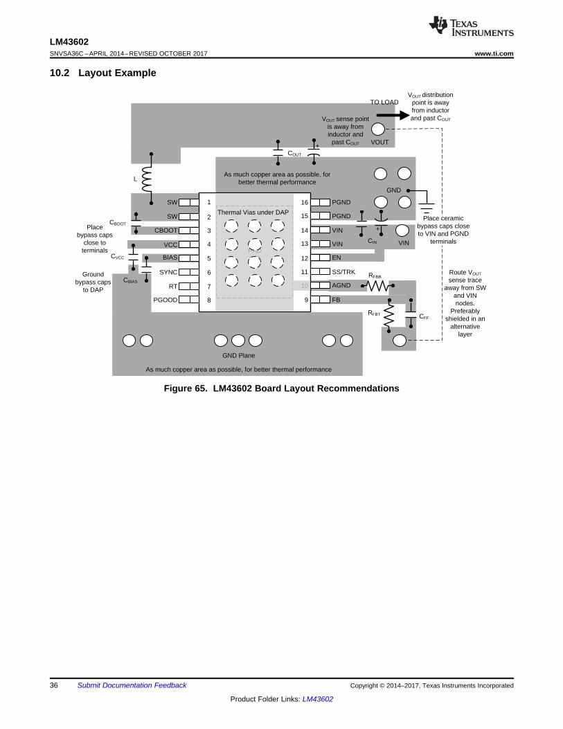
SW
VIN
PGND
CBOOT
VCC
BIAS
SYNC
RT
PGOOD
EN
SS/TRK
AGND
FB
SW PGND
VINPAD (17)
1 16
2
3
4
5
6
8
7
9
15
14
13
12
11
10
VIN
COUT
CBOOT
CIN
CVCC
VOUT
CBIAS
RFBT
RFBB
CFF
L
GND
Route VOUT sense trace
away from SW and VIN nodes.
Preferably shielded in an
alternative layer
GND Plane
VOUT sense point is away from inductor and
past COUT
Thermal Vias under DAP
As much copper area as possible, for better thermal performance
+
+
Place bypass caps
close to terminals
As much copper area as possible, for better thermal performance
VOUT distribution point is away from inductor and past COUT
TO LOAD
Ground bypass caps
to DAP
Place ceramic bypass caps close to VIN and PGND
terminals
36
LM43602SNVSA36C –APRIL 2014–REVISED OCTOBER 2017 www.ti.com
Product Folder Links: LM43602
Submit Documentation Feedback Copyright © 2014–2017, Texas Instruments Incorporated
10.2 Layout Example
Figure 65. LM43602 Board Layout Recommendations
37
LM43602www.ti.com SNVSA36C –APRIL 2014–REVISED OCTOBER 2017
Product Folder Links: LM43602
Submit Documentation FeedbackCopyright © 2014–2017, Texas Instruments Incorporated
11 Device and Documentation Support
11.1 Device Support
11.1.1 Development Support
11.1.1.1 Custom Design With WEBENCH® ToolsClick here to create a custom design using the LM43602 device with the WEBENCH® Power Designer.1. Start by entering the input voltage (VIN), output voltage (VOUT), and output current (IOUT) requirements.2. Optimize the design for key parameters such as efficiency, footprint, and cost using the optimizer dial.3. Compare the generated design with other possible solutions from Texas Instruments.
The WEBENCH Power Designer provides a customized schematic along with a list of materials with real-timepricing and component availability.
In most cases, these actions are available:• Run electrical simulations to see important waveforms and circuit performance• Run thermal simulations to understand board thermal performance• Export customized schematic and layout into popular CAD formats• Print PDF reports for the design, and share the design with colleagues
Get more information about WEBENCH tools at www.ti.com/WEBENCH.
11.2 Documentation Support
11.2.1 Related DocumentationFor related documentation see the following:• LM43602 EVM User's Guide (• Using New Thermal Metrics applications report (SBVA025).• Optimizing Transient Response of Internally Compensated dc-dc Converters With Feedforward Capacitor
(SLVA289).• Simple Success with Conducted EMI for DC-DC Converters (SNVA489).• AN-1149 Layout Guidelines for Switching Power Supplies SNVA021• AN-1229 Simple Switcher PCB Layout Guidelines SNVA054• Constructing Your Power Supply- Layout Considerations SLUP230• Low Radiated EMI Layout Made SIMPLE with LM4360x and LM4600x SNVA721• AN-2020 Thermal Design By Insight, Not Hindsight SNVA419• AN-1520 A Guide to Board Layout for Best Thermal Resistance for Exposed Pad Packages SNVA183• Semiconductor and IC Package Thermal Metrics SPRA953• Thermal Design made Simple with LM43603 and LM43602 SNVA719• PowerPAD™ Thermally Enhanced Package SLMA002• PowerPAD Made Easy SLMA004• Using New Thermal Metrics SBVA025
11.3 Related Links
Table 4. Related Links
PARTS PRODUCT FOLDER SAMPLE & BUY TECHNICALDOCUMENTS
TOOLS &SOFTWARE
SUPPORT &COMMUNITY
LM43603 Click here Click here Click here Click here Click here
38
LM43602SNVSA36C –APRIL 2014–REVISED OCTOBER 2017 www.ti.com
Product Folder Links: LM43602
Submit Documentation Feedback Copyright © 2014–2017, Texas Instruments Incorporated
11.4 Receiving Notification of Documentation UpdatesTo receive notification of documentation updates, navigate to the device product folder on ti.com. In the upperright corner, click on Alert me to register and receive a weekly digest of any product information that haschanged. For change details, review the revision history included in any revised document.
11.5 Community ResourcesThe following links connect to TI community resources. Linked contents are provided "AS IS" by the respectivecontributors. They do not constitute TI specifications and do not necessarily reflect TI's views; see TI's Terms ofUse.
TI E2E™ Online Community TI's Engineer-to-Engineer (E2E) Community. Created to foster collaborationamong engineers. At e2e.ti.com, you can ask questions, share knowledge, explore ideas and helpsolve problems with fellow engineers.
Design Support TI's Design Support Quickly find helpful E2E forums along with design support tools andcontact information for technical support.
11.6 TrademarksPowerPAD, E2E are trademarks of Texas Instruments.WEBENCH is a registered trademark of Texas Instruments.All other trademarks are the property of their respective owners.
11.7 Electrostatic Discharge CautionThis integrated circuit can be damaged by ESD. Texas Instruments recommends that all integrated circuits be handled withappropriate precautions. Failure to observe proper handling and installation procedures can cause damage.
ESD damage can range from subtle performance degradation to complete device failure. Precision integrated circuits may be moresusceptible to damage because very small parametric changes could cause the device not to meet its published specifications.
11.8 GlossarySLYZ022 — TI Glossary.
This glossary lists and explains terms, acronyms, and definitions.
12 Mechanical, Packaging, and Orderable InformationThe following pages include mechanical packaging and orderable information. This information is the mostcurrent data available for the designated devices. This data is subject to change without notice and revision ofthis document. For browser-based versions of this data sheet, refer to the left-hand navigation.
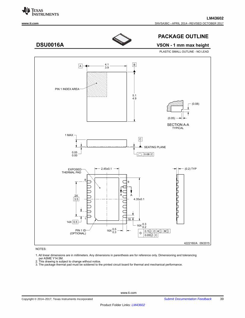
www.ti.com
PACKAGE OUTLINE
C
A A
16X0.30.2
4.35±0.1
2X
3.5
2.45±0.1
14X 0.5
1 MAX
16X0.50.3
0.050.00
A4.13.9
B
5.14.9
(0.2) TYP
(0.08)
(0.05)
VSON - 1 mm max heightDSU0016APLASTIC SMALL OUTLINE - NO LEAD
4222160/A 09/2015
PIN 1 INDEX AREA
SEATING PLANE
0.08 C
1
89
16
(OPTIONAL)PIN 1 ID 0.1 C A B
0.05 C
THERMAL PADEXPOSED
NOTES:
1. All linear dimensions are in millimeters. Any dimensions in parenthesis are for reference only. Dimensioning and tolerancingper ASME Y14.5M.
2. This drawing is subject to change without notice.3. The package thermal pad must be soldered to the printed circuit board for thermal and mechanical performance.
SCALE 3.000
SCALE 30.000
SECTION A-A
SECTION A-ATYPICAL
39
LM43602www.ti.com SNVSA36C –APRIL 2014–REVISED OCTOBER 2017
Product Folder Links: LM43602
Submit Documentation FeedbackCopyright © 2014–2017, Texas Instruments Incorporated
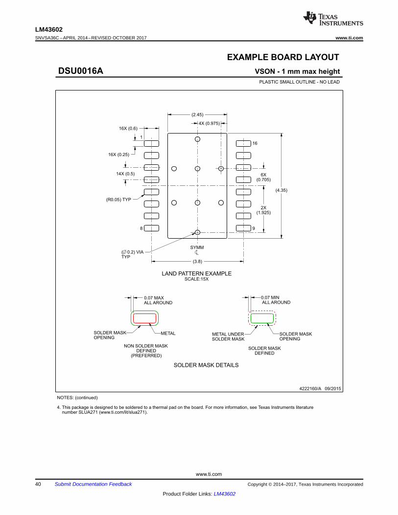
www.ti.com
EXAMPLE BOARD LAYOUT
0.07 MINALL AROUND
0.07 MAXALL AROUND
16X (0.25)
(4.35)
(3.8)
14X (0.5)
(2.45)
( ) VIATYP
0.2
4X (0.975)
2X(1.925)
16X (0.6)
(R ) TYP0.05
6X(0.705)
VSON - 1 mm max heightDSU0016APLASTIC SMALL OUTLINE - NO LEAD
4222160/A 09/2015
SYMM
1
8 9
16
SCALE:15XLAND PATTERN EXAMPLE
NOTES: (continued)
4. This package is designed to be soldered to a thermal pad on the board. For more information, see Texas Instruments literaturenumber SLUA271 (www.ti.com/lit/slua271).
SOLDER MASKOPENINGSOLDER MASK
METAL UNDER
SOLDER MASKDEFINED
METALSOLDER MASKOPENING
NON SOLDER MASK
SOLDER MASK DETAILS
DEFINED(PREFERRED)
40
LM43602SNVSA36C –APRIL 2014–REVISED OCTOBER 2017 www.ti.com
Product Folder Links: LM43602
Submit Documentation Feedback Copyright © 2014–2017, Texas Instruments Incorporated
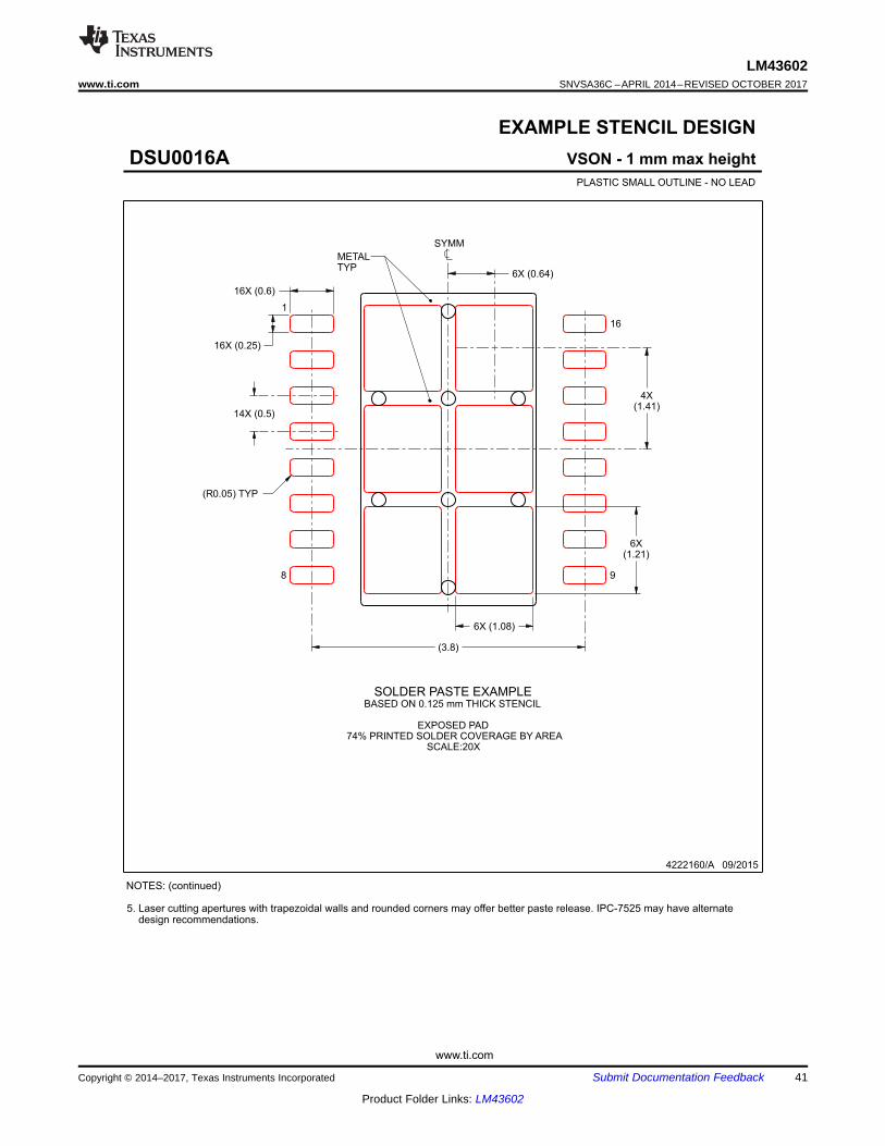
www.ti.com
EXAMPLE STENCIL DESIGN
(R ) TYP0.05
16X (0.25)
16X (0.6)
6X (1.08)
6X(1.21)
(3.8)
4X(1.41)
14X (0.5)
6X (0.64)
VSON - 1 mm max heightDSU0016APLASTIC SMALL OUTLINE - NO LEAD
4222160/A 09/2015
NOTES: (continued)
5. Laser cutting apertures with trapezoidal walls and rounded corners may offer better paste release. IPC-7525 may have alternatedesign recommendations.
SOLDER PASTE EXAMPLEBASED ON 0.125 mm THICK STENCIL
EXPOSED PAD74% PRINTED SOLDER COVERAGE BY AREA
SCALE:20X
SYMM
1
8 9
16
METALTYP
41
LM43602www.ti.com SNVSA36C –APRIL 2014–REVISED OCTOBER 2017
Product Folder Links: LM43602
Submit Documentation FeedbackCopyright © 2014–2017, Texas Instruments Incorporated
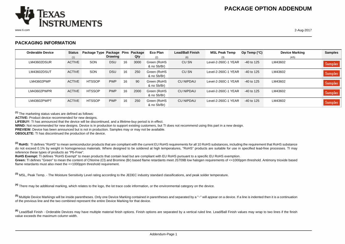
PACKAGE OPTION ADDENDUM
www.ti.com 2-Aug-2017
Addendum-Page 1
PACKAGING INFORMATION
Orderable Device Status(1)
Package Type PackageDrawing
Pins PackageQty
Eco Plan(2)
Lead/Ball Finish(6)
MSL Peak Temp(3)
Op Temp (°C) Device Marking(4/5)
Samples
LM43602DSUR ACTIVE SON DSU 16 3000 Green (RoHS& no Sb/Br)
CU SN Level-2-260C-1 YEAR -40 to 125 LM43602
LM43602DSUT ACTIVE SON DSU 16 250 Green (RoHS& no Sb/Br)
CU SN Level-2-260C-1 YEAR -40 to 125 LM43602
LM43602PWP ACTIVE HTSSOP PWP 16 90 Green (RoHS& no Sb/Br)
CU NIPDAU Level-2-260C-1 YEAR -40 to 125 LM43602
LM43602PWPR ACTIVE HTSSOP PWP 16 2000 Green (RoHS& no Sb/Br)
CU NIPDAU Level-2-260C-1 YEAR -40 to 125 LM43602
LM43602PWPT ACTIVE HTSSOP PWP 16 250 Green (RoHS& no Sb/Br)
CU NIPDAU Level-2-260C-1 YEAR -40 to 125 LM43602
(1) The marketing status values are defined as follows:ACTIVE: Product device recommended for new designs.LIFEBUY: TI has announced that the device will be discontinued, and a lifetime-buy period is in effect.NRND: Not recommended for new designs. Device is in production to support existing customers, but TI does not recommend using this part in a new design.PREVIEW: Device has been announced but is not in production. Samples may or may not be available.OBSOLETE: TI has discontinued the production of the device.
(2) RoHS: TI defines "RoHS" to mean semiconductor products that are compliant with the current EU RoHS requirements for all 10 RoHS substances, including the requirement that RoHS substancedo not exceed 0.1% by weight in homogeneous materials. Where designed to be soldered at high temperatures, "RoHS" products are suitable for use in specified lead-free processes. TI mayreference these types of products as "Pb-Free".RoHS Exempt: TI defines "RoHS Exempt" to mean products that contain lead but are compliant with EU RoHS pursuant to a specific EU RoHS exemption.Green: TI defines "Green" to mean the content of Chlorine (Cl) and Bromine (Br) based flame retardants meet JS709B low halogen requirements of <=1000ppm threshold. Antimony trioxide basedflame retardants must also meet the <=1000ppm threshold requirement.
(3) MSL, Peak Temp. - The Moisture Sensitivity Level rating according to the JEDEC industry standard classifications, and peak solder temperature.
(4) There may be additional marking, which relates to the logo, the lot trace code information, or the environmental category on the device.
(5) Multiple Device Markings will be inside parentheses. Only one Device Marking contained in parentheses and separated by a "~" will appear on a device. If a line is indented then it is a continuationof the previous line and the two combined represent the entire Device Marking for that device.
(6) Lead/Ball Finish - Orderable Devices may have multiple material finish options. Finish options are separated by a vertical ruled line. Lead/Ball Finish values may wrap to two lines if the finishvalue exceeds the maximum column width.
PACKAGE OPTION ADDENDUM
www.ti.com 2-Aug-2017
Addendum-Page 2
Important Information and Disclaimer:The information provided on this page represents TI's knowledge and belief as of the date that it is provided. TI bases its knowledge and belief on informationprovided by third parties, and makes no representation or warranty as to the accuracy of such information. Efforts are underway to better integrate information from third parties. TI has taken andcontinues to take reasonable steps to provide representative and accurate information but may not have conducted destructive testing or chemical analysis on incoming materials and chemicals.TI and TI suppliers consider certain information to be proprietary, and thus CAS numbers and other limited information may not be available for release.
In no event shall TI's liability arising out of such information exceed the total purchase price of the TI part(s) at issue in this document sold by TI to Customer on an annual basis.
OTHER QUALIFIED VERSIONS OF LM43602 :
• Automotive: LM43602-Q1
NOTE: Qualified Version Definitions:
• Automotive - Q100 devices qualified for high-reliability automotive applications targeting zero defects
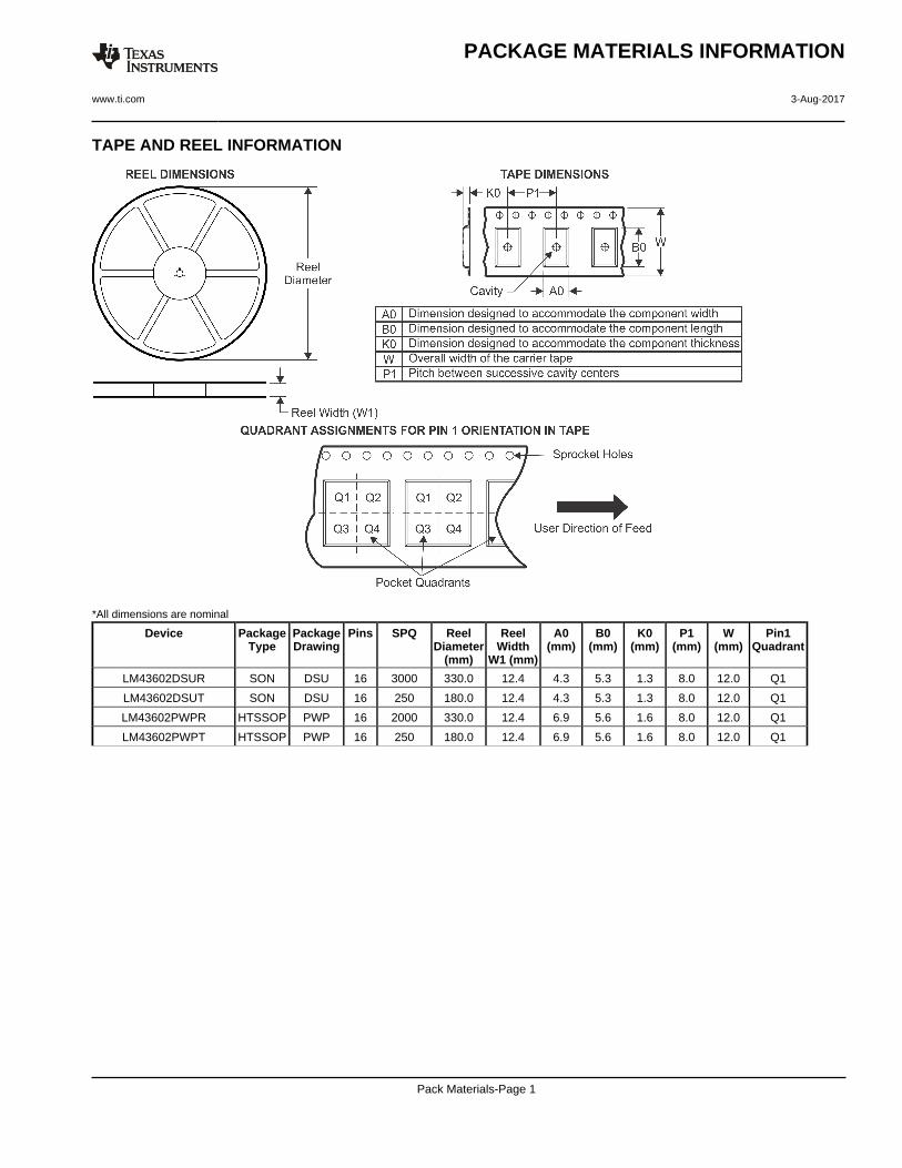
TAPE AND REEL INFORMATION
*All dimensions are nominal
Device PackageType
PackageDrawing
Pins SPQ ReelDiameter
(mm)
ReelWidth
W1 (mm)
A0(mm)
B0(mm)
K0(mm)
P1(mm)
W(mm)
Pin1Quadrant
LM43602DSUR SON DSU 16 3000 330.0 12.4 4.3 5.3 1.3 8.0 12.0 Q1
LM43602DSUT SON DSU 16 250 180.0 12.4 4.3 5.3 1.3 8.0 12.0 Q1
LM43602PWPR HTSSOP PWP 16 2000 330.0 12.4 6.9 5.6 1.6 8.0 12.0 Q1
LM43602PWPT HTSSOP PWP 16 250 180.0 12.4 6.9 5.6 1.6 8.0 12.0 Q1
PACKAGE MATERIALS INFORMATION
www.ti.com 3-Aug-2017
Pack Materials-Page 1
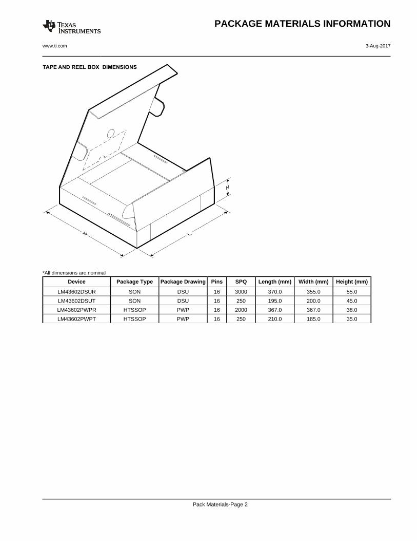
*All dimensions are nominal
Device Package Type Package Drawing Pins SPQ Length (mm) Width (mm) Height (mm)
LM43602DSUR SON DSU 16 3000 370.0 355.0 55.0
LM43602DSUT SON DSU 16 250 195.0 200.0 45.0
LM43602PWPR HTSSOP PWP 16 2000 367.0 367.0 38.0
LM43602PWPT HTSSOP PWP 16 250 210.0 185.0 35.0
PACKAGE MATERIALS INFORMATION
www.ti.com 3-Aug-2017
Pack Materials-Page 2
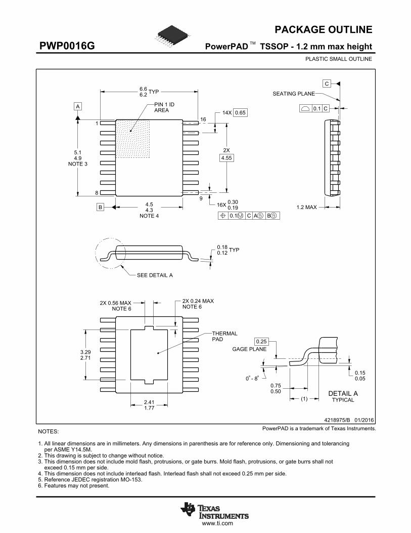
www.ti.com
PACKAGE OUTLINE
C TYP6.6
6.2
1.2 MAX
14X 0.65
16X 0.300.19
2X4.55
TYP0.180.12
0 - 80.150.05
2.411.77
3.292.71
2X 0.56 MAXNOTE 6
(1)
0.25GAGE PLANE
0.750.50
A
NOTE 3
5.14.9
BNOTE 4
4.54.3
2X 0.24 MAXNOTE 6
4218975/B 01/2016
PowerPAD TSSOP - 1.2 mm max heightPWP0016GPLASTIC SMALL OUTLINE
NOTES: 1. All linear dimensions are in millimeters. Any dimensions in parenthesis are for reference only. Dimensioning and tolerancing per ASME Y14.5M. 2. This drawing is subject to change without notice. 3. This dimension does not include mold flash, protrusions, or gate burrs. Mold flash, protrusions, or gate burrs shall not exceed 0.15 mm per side. 4. This dimension does not include interlead flash. Interlead flash shall not exceed 0.25 mm per side.5. Reference JEDEC registration MO-153.6. Features may not present.
PowerPAD is a trademark of Texas Instruments.
TM
116
0.1 C A B
98
PIN 1 IDAREA
SEATING PLANE
0.1 C
SEE DETAIL A
DETAIL ATYPICAL
SCALE 2.400
THERMALPAD
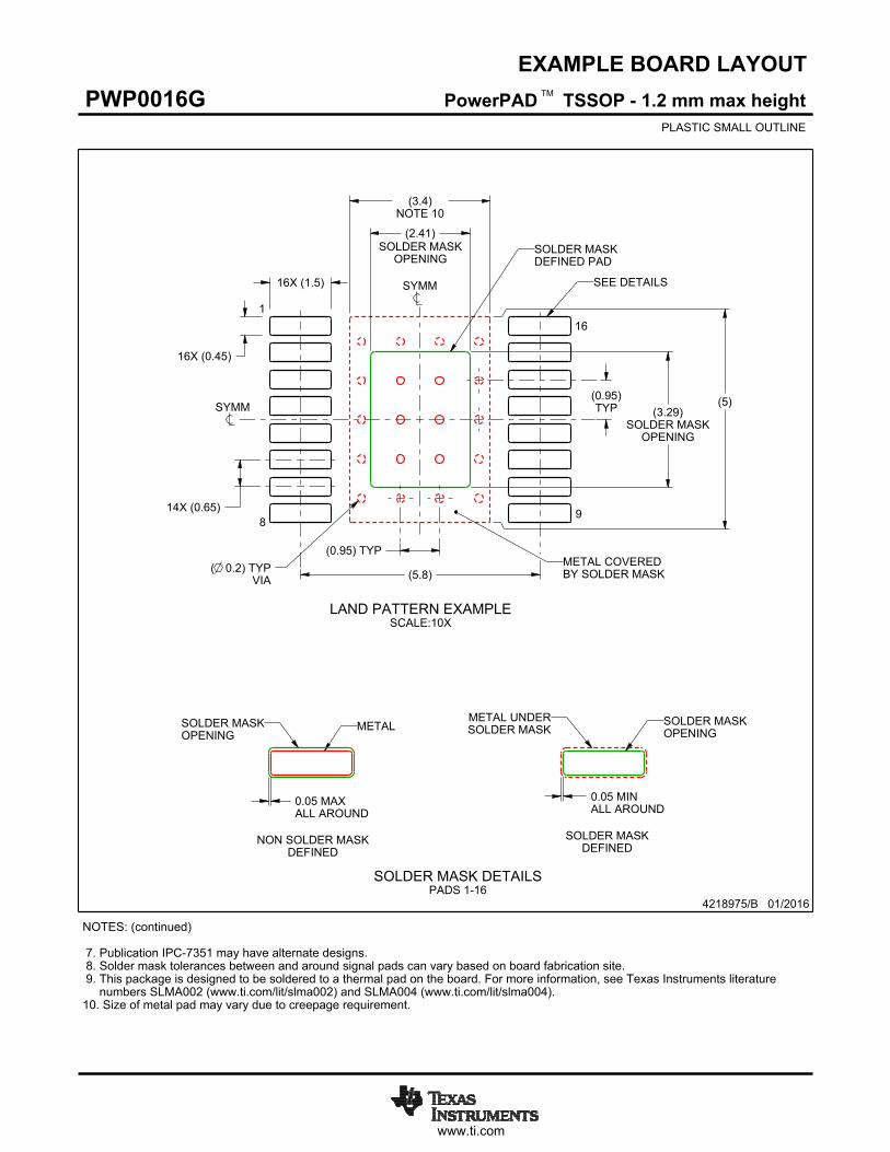
www.ti.com
EXAMPLE BOARD LAYOUT
(5.8)
0.05 MAXALL AROUND
0.05 MINALL AROUND
16X (1.5)
16X (0.45)
14X (0.65)
(3.4)NOTE 10
(5)
(2.41)
(3.29)SOLDER MASK
OPENING
( ) TYPVIA
0.2(0.95) TYP
(0.95)TYP
4218975/B 01/2016
PowerPAD TSSOP - 1.2 mm max heightPWP0016GPLASTIC SMALL OUTLINE
SYMM
SYMM
SEE DETAILS
LAND PATTERN EXAMPLESCALE:10X
1
89
16
SOLDER MASKOPENING
METAL COVEREDBY SOLDER MASK
SOLDER MASKDEFINED PAD
NOTES: (continued) 7. Publication IPC-7351 may have alternate designs. 8. Solder mask tolerances between and around signal pads can vary based on board fabrication site. 9. This package is designed to be soldered to a thermal pad on the board. For more information, see Texas Instruments literature numbers SLMA002 (www.ti.com/lit/slma002) and SLMA004 (www.ti.com/lit/slma004).10. Size of metal pad may vary due to creepage requirement.
TM
METALSOLDER MASKOPENING
NON SOLDER MASKDEFINED
SOLDER MASK DETAILSPADS 1-16
SOLDER MASKDEFINED
SOLDER MASKMETAL UNDER SOLDER MASK
OPENING
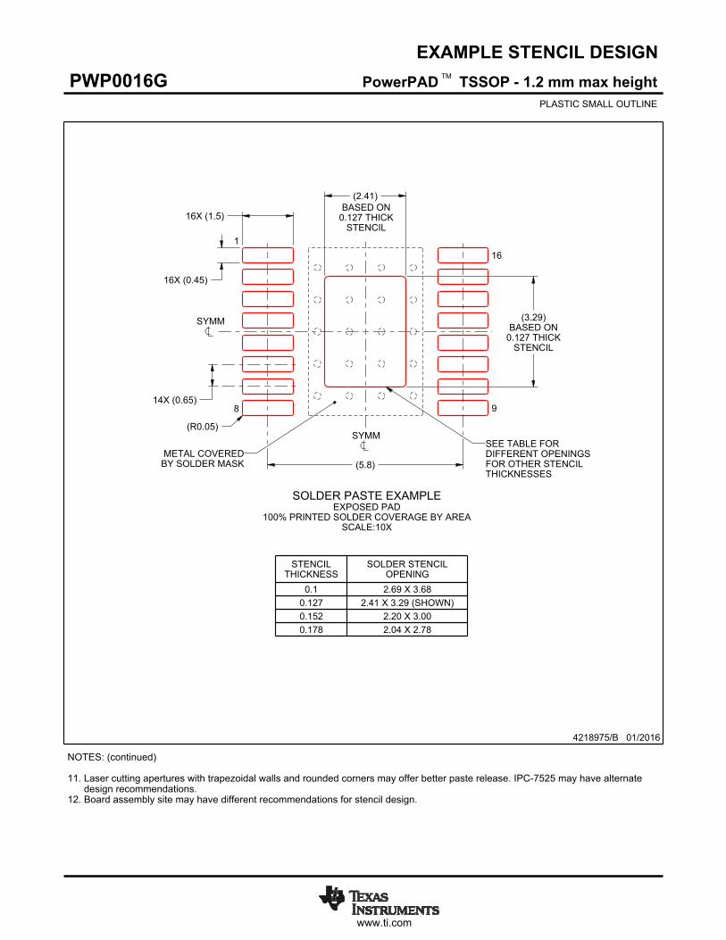
www.ti.com
EXAMPLE STENCIL DESIGN
16X (1.5)
16X (0.45)
(2.41)
(3.29)BASED ON
0.127 THICKSTENCIL
(5.8)
14X (0.65)
(R )0.05
4218975/B 01/2016
PowerPAD TSSOP - 1.2 mm max heightPWP0016GPLASTIC SMALL OUTLINE
2.04 X 2.780.1782.20 X 3.000.152
2.41 X 3.29 (SHOWN)0.1272.69 X 3.680.1
SOLDER STENCILOPENING
STENCILTHICKNESS
NOTES: (continued) 11. Laser cutting apertures with trapezoidal walls and rounded corners may offer better paste release. IPC-7525 may have alternate design recommendations. 12. Board assembly site may have different recommendations for stencil design.
TM
SYMM
SYMM
1
8 9
16
BASED ON0.127 THICK
STENCIL
BY SOLDER MASKMETAL COVERED
SEE TABLE FORDIFFERENT OPENINGSFOR OTHER STENCILTHICKNESSES
SOLDER PASTE EXAMPLEEXPOSED PAD
100% PRINTED SOLDER COVERAGE BY AREASCALE:10X
IMPORTANT NOTICE
Texas Instruments Incorporated (TI) reserves the right to make corrections, enhancements, improvements and other changes to itssemiconductor products and services per JESD46, latest issue, and to discontinue any product or service per JESD48, latest issue. Buyersshould obtain the latest relevant information before placing orders and should verify that such information is current and complete.TI’s published terms of sale for semiconductor products (http://www.ti.com/sc/docs/stdterms.htm) apply to the sale of packaged integratedcircuit products that TI has qualified and released to market. Additional terms may apply to the use or sale of other types of TI products andservices.Reproduction of significant portions of TI information in TI data sheets is permissible only if reproduction is without alteration and isaccompanied by all associated warranties, conditions, limitations, and notices. TI is not responsible or liable for such reproduceddocumentation. Information of third parties may be subject to additional restrictions. Resale of TI products or services with statementsdifferent from or beyond the parameters stated by TI for that product or service voids all express and any implied warranties for theassociated TI product or service and is an unfair and deceptive business practice. TI is not responsible or liable for any such statements.Buyers and others who are developing systems that incorporate TI products (collectively, “Designers”) understand and agree that Designersremain responsible for using their independent analysis, evaluation and judgment in designing their applications and that Designers havefull and exclusive responsibility to assure the safety of Designers' applications and compliance of their applications (and of all TI productsused in or for Designers’ applications) with all applicable regulations, laws and other applicable requirements. Designer represents that, withrespect to their applications, Designer has all the necessary expertise to create and implement safeguards that (1) anticipate dangerousconsequences of failures, (2) monitor failures and their consequences, and (3) lessen the likelihood of failures that might cause harm andtake appropriate actions. Designer agrees that prior to using or distributing any applications that include TI products, Designer willthoroughly test such applications and the functionality of such TI products as used in such applications.TI’s provision of technical, application or other design advice, quality characterization, reliability data or other services or information,including, but not limited to, reference designs and materials relating to evaluation modules, (collectively, “TI Resources”) are intended toassist designers who are developing applications that incorporate TI products; by downloading, accessing or using TI Resources in anyway, Designer (individually or, if Designer is acting on behalf of a company, Designer’s company) agrees to use any particular TI Resourcesolely for this purpose and subject to the terms of this Notice.TI’s provision of TI Resources does not expand or otherwise alter TI’s applicable published warranties or warranty disclaimers for TIproducts, and no additional obligations or liabilities arise from TI providing such TI Resources. TI reserves the right to make corrections,enhancements, improvements and other changes to its TI Resources. TI has not conducted any testing other than that specificallydescribed in the published documentation for a particular TI Resource.Designer is authorized to use, copy and modify any individual TI Resource only in connection with the development of applications thatinclude the TI product(s) identified in such TI Resource. NO OTHER LICENSE, EXPRESS OR IMPLIED, BY ESTOPPEL OR OTHERWISETO ANY OTHER TI INTELLECTUAL PROPERTY RIGHT, AND NO LICENSE TO ANY TECHNOLOGY OR INTELLECTUAL PROPERTYRIGHT OF TI OR ANY THIRD PARTY IS GRANTED HEREIN, including but not limited to any patent right, copyright, mask work right, orother intellectual property right relating to any combination, machine, or process in which TI products or services are used. Informationregarding or referencing third-party products or services does not constitute a license to use such products or services, or a warranty orendorsement thereof. Use of TI Resources may require a license from a third party under the patents or other intellectual property of thethird party, or a license from TI under the patents or other intellectual property of TI.TI RESOURCES ARE PROVIDED “AS IS” AND WITH ALL FAULTS. TI DISCLAIMS ALL OTHER WARRANTIES ORREPRESENTATIONS, EXPRESS OR IMPLIED, REGARDING RESOURCES OR USE THEREOF, INCLUDING BUT NOT LIMITED TOACCURACY OR COMPLETENESS, TITLE, ANY EPIDEMIC FAILURE WARRANTY AND ANY IMPLIED WARRANTIES OFMERCHANTABILITY, FITNESS FOR A PARTICULAR PURPOSE, AND NON-INFRINGEMENT OF ANY THIRD PARTY INTELLECTUALPROPERTY RIGHTS. TI SHALL NOT BE LIABLE FOR AND SHALL NOT DEFEND OR INDEMNIFY DESIGNER AGAINST ANY CLAIM,INCLUDING BUT NOT LIMITED TO ANY INFRINGEMENT CLAIM THAT RELATES TO OR IS BASED ON ANY COMBINATION OFPRODUCTS EVEN IF DESCRIBED IN TI RESOURCES OR OTHERWISE. IN NO EVENT SHALL TI BE LIABLE FOR ANY ACTUAL,DIRECT, SPECIAL, COLLATERAL, INDIRECT, PUNITIVE, INCIDENTAL, CONSEQUENTIAL OR EXEMPLARY DAMAGES INCONNECTION WITH OR ARISING OUT OF TI RESOURCES OR USE THEREOF, AND REGARDLESS OF WHETHER TI HAS BEENADVISED OF THE POSSIBILITY OF SUCH DAMAGES.Unless TI has explicitly designated an individual product as meeting the requirements of a particular industry standard (e.g., ISO/TS 16949and ISO 26262), TI is not responsible for any failure to meet such industry standard requirements.Where TI specifically promotes products as facilitating functional safety or as compliant with industry functional safety standards, suchproducts are intended to help enable customers to design and create their own applications that meet applicable functional safety standardsand requirements. Using products in an application does not by itself establish any safety features in the application. Designers mustensure compliance with safety-related requirements and standards applicable to their applications. Designer may not use any TI products inlife-critical medical equipment unless authorized officers of the parties have executed a special contract specifically governing such use.Life-critical medical equipment is medical equipment where failure of such equipment would cause serious bodily injury or death (e.g., lifesupport, pacemakers, defibrillators, heart pumps, neurostimulators, and implantables). Such equipment includes, without limitation, allmedical devices identified by the U.S. Food and Drug Administration as Class III devices and equivalent classifications outside the U.S.TI may expressly designate certain products as completing a particular qualification (e.g., Q100, Military Grade, or Enhanced Product).Designers agree that it has the necessary expertise to select the product with the appropriate qualification designation for their applicationsand that proper product selection is at Designers’ own risk. Designers are solely responsible for compliance with all legal and regulatoryrequirements in connection with such selection.Designer will fully indemnify TI and its representatives against any damages, costs, losses, and/or liabilities arising out of Designer’s non-compliance with the terms and provisions of this Notice.
Mailing Address: Texas Instruments, Post Office Box 655303, Dallas, Texas 75265Copyright © 2017, Texas Instruments Incorporated