LM73605/LM73606 3.5-V to 36-V, 5-A or 6-A … · vcc rt bias ss/trk 2 3 4 23 25 24 pvin sw sw dap...
53
SW PVIN PGND CBOOT VCC BIAS EN AGND FB VIN COUT CBOOT CIN CVCC VOUT RFBT RFBB L SYNC/ MODE RT SS/TRK PGOOD Copyright © 2017, Texas Instruments Incorporated Load Current (A) Efficiency (%) 0.001 0.01 0.02 0.05 0.1 0.2 0.5 1 2 3 4 56 50 55 60 65 70 75 80 85 90 95 100 Eff_ VIN = 12 V VIN = 24 V Product Folder Order Now Technical Documents Tools & Software Support & Community Reference Design An IMPORTANT NOTICE at the end of this data sheet addresses availability, warranty, changes, use in safety-critical applications, intellectual property matters and other important disclaimers. PRODUCTION DATA. LM73605, LM73606 SNVSAH5 – SEPTEMBER 2017 LM73605/LM73606 3.5-V to 36-V, 5-A or 6-A Synchronous Step-Down Voltage Converter 1 1 Features 1• Synchronous Rectification • Wettable Flanks QFN Package (WQFN) • Low Quiescent Current – 0.8 μA in Shutdown (typical) – 15 μA in Active Mode with No Load (typical) • Wide Voltage Conversion Range: – t ON_MIN = 60 ns (typical) – t OFF_MIN = 70 ns (typical) • Low MOSFET ON-Resistance: – R DS_ON_HS = 53 mΩ (typical) – R DS_ON_LS = 31 mΩ (typical) • External Bias Input to Improve Efficiency • Pin-Selectable Auto Mode or Forced PWM Operation • Adjustable Frequency Range: 350 kHz to 2.2 MHz • Synchronizable to External Clock • Internal Compensation • Power-Good Flag • Precision Enable to Program System UVLO • Flexible Soft-Start Features: – Start-up into Pre-Biased Load – Fixed or Adjustable Soft-Start Time – Output Voltage Tracking • Cycle-by-Cycle Current Limiting • Short-Circuit Protection With Hiccup Mode • Thermal Shutdown Protection • Create a Custom Design With the WEBENCH ® Power Designer using LM73605 or LM73606 Simplified Schematic 2 Applications • Industrial Distributed Power Applications • Telecommunications Systems • General-Purpose Wide V IN Regulation 3 Description The LM73605/LM73606 family of devices are easy- to-use synchronous step-down DC-DC converters capable of driving up to 5 A (LM73605) or 6 A (LM73606) of load current from a supply voltage ranging from 3.5 V to 36 V. The LM73605/LM73606 provide exceptional efficiency and output accuracy in a very small solution size. Peak current-mode control is employed. Additional features such as adjustable switching frequency, synchronization to an external clock, FPWM option, power-good flag, precision enable, adjustable soft start, and tracking provide both flexible and easy-to-use solutions for a wide range of applications. Automatic frequency foldback at light load and optional external bias improve efficiency over the entire load range. The family requires few external components and has a pinout designed for simple PCB layout with optimal EMI and thermal performance. Protection features include thermal shutdown, input undervoltage lockout, cycle- by-cycle current limiting, and hiccup short-circuit protection. The LM73605 and LM73606 devices are pin-to-pin compatible for easy current scaling. Device Information (1) PART NUMBER PACKAGE BODY SIZE (NOM) LM73605 WQFN (30) Wettable Flanks 6.00 mm × 4.00 mm LM73606 (1) For all available packages, see the orderable addendum at the end of the data sheet. Efficiency vs Load Current V OUT = 5 V, f SW = 500 kHz, Auto Mode
Transcript of LM73605/LM73606 3.5-V to 36-V, 5-A or 6-A … · vcc rt bias ss/trk 2 3 4 23 25 24 pvin sw sw dap...
SWPVIN
PGNDCBOOT
VCC
BIAS
EN
AGND
FB
VIN
COUTCBOOTCIN
CVCC
VOUT
RFBT
RFBB
L
SYNC/MODE
RTSS/TRK
PGOOD
Copyright © 2017, Texas Instruments Incorporated
Load Current (A)
Effi
cien
cy (
%)
0.001 0.01 0.02 0.05 0.1 0.2 0.5 1 2 3 4 5650
55
60
65
70
75
80
85
90
95
100
Eff_
VIN = 12 VVIN = 24 V
Product
Folder
Order
Now
Technical
Documents
Tools &
Software
Support &Community
ReferenceDesign
An IMPORTANT NOTICE at the end of this data sheet addresses availability, warranty, changes, use in safety-critical applications,intellectual property matters and other important disclaimers. PRODUCTION DATA.
LM73605, LM73606SNVSAH5 –SEPTEMBER 2017
LM73605/LM73606 3.5-V to 36-V, 5-A or 6-A SynchronousStep-Down Voltage Converter
1
1 Features1• Synchronous Rectification• Wettable Flanks QFN Package (WQFN)• Low Quiescent Current
– 0.8 µA in Shutdown (typical)– 15 µA in Active Mode with No Load (typical)
• Wide Voltage Conversion Range:– tON_MIN = 60 ns (typical)– tOFF_MIN = 70 ns (typical)
• Low MOSFET ON-Resistance:– RDS_ON_HS = 53 mΩ (typical)– RDS_ON_LS = 31 mΩ (typical)
• External Bias Input to Improve Efficiency• Pin-Selectable Auto Mode or Forced PWM
Operation• Adjustable Frequency Range: 350 kHz to 2.2 MHz• Synchronizable to External Clock• Internal Compensation• Power-Good Flag• Precision Enable to Program System UVLO• Flexible Soft-Start Features:
– Start-up into Pre-Biased Load– Fixed or Adjustable Soft-Start Time– Output Voltage Tracking
• Cycle-by-Cycle Current Limiting• Short-Circuit Protection With Hiccup Mode• Thermal Shutdown Protection• Create a Custom Design With the WEBENCH®
Power Designer using LM73605 or LM73606
Simplified Schematic
2 Applications• Industrial Distributed Power Applications• Telecommunications Systems• General-Purpose Wide VIN Regulation
3 DescriptionThe LM73605/LM73606 family of devices are easy-to-use synchronous step-down DC-DC converterscapable of driving up to 5 A (LM73605) or 6 A(LM73606) of load current from a supply voltageranging from 3.5 V to 36 V. The LM73605/LM73606provide exceptional efficiency and output accuracy ina very small solution size. Peak current-mode controlis employed. Additional features such as adjustableswitching frequency, synchronization to an externalclock, FPWM option, power-good flag, precisionenable, adjustable soft start, and tracking provideboth flexible and easy-to-use solutions for a widerange of applications. Automatic frequency foldbackat light load and optional external bias improveefficiency over the entire load range. The familyrequires few external components and has a pinoutdesigned for simple PCB layout with optimal EMI andthermal performance. Protection features includethermal shutdown, input undervoltage lockout, cycle-by-cycle current limiting, and hiccup short-circuitprotection. The LM73605 and LM73606 devices arepin-to-pin compatible for easy current scaling.
Device Information(1)
PART NUMBER PACKAGE BODY SIZE (NOM)LM73605 WQFN (30)
Wettable Flanks 6.00 mm × 4.00 mmLM73606
(1) For all available packages, see the orderable addendum atthe end of the data sheet.
Efficiency vs Load CurrentVOUT = 5 V, fSW = 500 kHz, Auto Mode
2
LM73605, LM73606SNVSAH5 –SEPTEMBER 2017 www.ti.com
Product Folder Links: LM73605 LM73606
Submit Documentation Feedback Copyright © 2017, Texas Instruments Incorporated
Table of Contents1 Features .................................................................. 12 Applications ........................................................... 13 Description ............................................................. 14 Revision History..................................................... 25 Pin Configuration and Functions ......................... 36 Specifications......................................................... 5
6.1 Absolute Maximum Ratings ...................................... 56.2 ESD Ratings.............................................................. 56.3 Recommended Operating Conditions....................... 56.4 Thermal Information .................................................. 66.5 Electrical Characteristics........................................... 66.6 Timing Characteristics............................................... 76.7 Switching Characteristics .......................................... 86.8 System Characteristics ............................................. 86.9 Typical Characteristics .............................................. 9
7 Detailed Description ............................................ 117.1 Overview ................................................................. 117.2 Functional Block Diagram ....................................... 117.3 Feature Description................................................. 12
7.4 Device Functional Modes........................................ 238 Application and Implementation ........................ 25
8.1 Application Information............................................ 258.2 Typical Application ................................................. 25
9 Power Supply Recommendations ...................... 3910 Layout................................................................... 39
10.1 Layout Guidelines ................................................. 3910.2 Layout Example .................................................... 42
11 Device and Documentation Support ................. 4311.1 Device Support...................................................... 4311.2 Related Documentation ....................................... 4311.3 Related Links ........................................................ 4311.4 Receiving Notification of Documentation Updates 4311.5 Community Resources.......................................... 4411.6 Trademarks ........................................................... 4411.7 Electrostatic Discharge Caution............................ 4411.8 Glossary ................................................................ 44
12 Mechanical, Packaging, and OrderableInformation ........................................................... 45
4 Revision History
DATE REVISION NOTESSeptember 2017 * Initial release
VCC
RT
BIAS
SS/TRK
2
3
4 23
25
24
PVIN
SW
SW
DAP PVIN
PGNDSW
22
261
5
CBOOT
SW
PGND
216
PGND
PGND
207
PGOOD
198 AGND
9
10
18
17
EN
FB
SYNC/MODE
1611
29 28 2730
13 14 1512
SW PVIN
NC NC NC NC
NC NC NC NC
3
LM73605, LM73606www.ti.com SNVSAH5 –SEPTEMBER 2017
Product Folder Links: LM73605 LM73606
Submit Documentation FeedbackCopyright © 2017, Texas Instruments Incorporated
(1) A = Analog, O = Output, I = Input, G = Ground, P = Power
5 Pin Configuration and Functions
RNP Package30-Pin Wettable Flanks QFN (WQFN) 6 mm × 4 mm × 0.8 mm
Top View
Pin FunctionsPIN
I/O (1) DESCRIPTIONNO. NAME
1, 2, 3, 4, 5 SW P Switching output of the regulator. Internally connected to source of the HS FET and drain of the LSFET. Connect to power inductor and boot-strap capacitor.
6 CBOOT P Boot-strap capacitor connection for HS FET driver. Connect a high-quality 470-nF capacitor fromthis pin to the SW pin.
7 VCC POutput of internal bias supply. Used as supply to internal control circuits and drivers. Connect ahigh-quality 2.2-µF capacitor from this pin to GND. TI does not recommend loading this pin byexternal circuitry.
8 BIAS POptional BIAS LDO supply input. TI recommends tying to VOUT when 3.3 V ≤ VOUT ≤ 18 V, or tie toan external 3.3-V or 5-V rail if available, to improve efficiency. BIAS pin voltage must not begreater than VIN. Tie to ground when not in use.
9 RT A Switching frequency setting pin. Place a resistor from this pin to ground to set the switchingfrequency. If floating, the default switching frequency will be 500 kHz. Do not short to ground.
10 SS/TRK A
Soft-start control pin. Leave this pin floating for a 5-ms internal soft-start ramp. An externalcapacitor can be connected from this pin to ground to extend the soft start time. A 2-µA currentsourced from this pin charges the capacitor to provide the ramp. Connect to external ramp fortracking. Do not short to ground.
11 FB I Feedback input for output voltage regulation. Connect a resistor divider to set the output voltage.Never short this pin to ground during operation.
12–15,27–30 NC — No internal connection. Connect to ground net and copper to improve heat sinking and board-level
reliability.
16 PGOOD OOpen drain power-good flag output. Connect to suitable voltage supply through a current limitingresistor. High = VOUT regulation OK, Low = VOUT regulation fault. PGOOD = LOW when EN = lowand VIN > 2 V.
4
LM73605, LM73606SNVSAH5 –SEPTEMBER 2017 www.ti.com
Product Folder Links: LM73605 LM73606
Submit Documentation Feedback Copyright © 2017, Texas Instruments Incorporated
Pin Functions (continued)PIN
I/O (1) DESCRIPTIONNO. NAME
17 SYNC/MODE I
Synchronization input and mode setting pin. Do not float. Tie to ground if not used.Tie to ground: auto mode, higher efficiency at light loads;Tie to logic high: forced PWM, constant switching frequency over load;Tie to external clock source: forced PWM, synchronize to the rising edge of the external clock.
18 EN I Enable input to regulator. Do not float. High = ON, Low = OFF. Can be tied to PVIN. Precisionenable input allows adjustable input voltage UVLO using external resistor divider.
19 AGND G Analog ground. Ground reference for internal circuitry. All electrical parameters are measured withrespect to this pin. Connect to system ground on PCB.
20–22 PVIN PSupply input to internal bias LDO and HS FET. Connect to input supply and input bypasscapacitors CIN. CIN must be placed right next to this pin and PGND pins on PCB, and connectedwith short and wide traces.
23–26 PGND G Power ground, connected to the source of LS FET internally. Connect to system ground, DAP/EP,AGND, ground side of CIN and COUT on PCB. Path to CIN must be as short as possible
EP DAP GLow impedance connection to AGND. Connect to system ground on PCB. Major heat dissipationpath for the device. Must be used for heat sinking by soldering to ground copper on PCB. Thermalvias are preferred to improve heat dissipation to other layers.
5
LM73605, LM73606www.ti.com SNVSAH5 –SEPTEMBER 2017
Product Folder Links: LM73605 LM73606
Submit Documentation FeedbackCopyright © 2017, Texas Instruments Incorporated
(1) Stresses beyond those listed under Absolute Maximum Ratings may cause permanent damage to the device. These are stress ratingsonly, which do not imply functional operation of the device at these or any other conditions beyond those indicated under RecommendedOperating Conditions. Exposure to absolute-maximum-rated conditions for extended periods may affect device reliability.
6 Specifications
6.1 Absolute Maximum RatingsOver operating free-air temperature range of –40°C to +125°C (unless otherwise noted) (1)
PARAMETER MIN MAX UNIT
Input voltages
PVIN to PGND –0.3 42
V
EN to AGND –0.3 VIN + 0.3FB, RT, SS/TRK to AGND –0.3 5PGOOD to AGND –0.1 20SYNC to AGND –0.3 5.5BIAS to AGND –0.3 Lower of (VIN + 0.3) or 20AGND to PGND –0.3 0.3
Output voltages
SW to PGND –0.3 VIN + 0.3
VSW to PGND less than 10-ns transients –3.5 42CBOOT to SW –0.3 5VCC to AGND –0.3 5
Operating junction temperature, TJ –40 150 °CStorage temperature, Tstg –65 150 °C
(1) JEDEC document JEP155 states that 500-V HBM allows safe manufacturing with a standard ESD control process.(2) JEDEC document JEP157 states that 250-V CDM allows safe manufacturing with a standard ESD control process.
6.2 ESD RatingsVALUE UNIT
V(ESD) Electrostatic dischargeHuman-body model (HBM), per ANSI/ESDA/JEDEC JS-001 (1) ±2000
VCharged-device model (CDM), per JEDEC specification JESD22-C101 (2) ±750
(1) Recommended operating rating indicate conditions for which the device is intended to be functional, but do not ensure specificperformance limits. For ensured specifications, see Electrical Characteristics
6.3 Recommended Operating ConditionsOver operating free-air temperature range of –40°C to +125°C (unless otherwise noted) (1)
MIN MAX UNIT
Input voltages
PVIN to PGND 3.5 36
V
EN 0 VIN
FB 0 4.5PGOOD 0 18BIAS input not used 0 0.3BIAS input used 0 Lower of (VIN + 0.3) or 18AGND to PGND –0.1 0.1
Output voltage VOUT 1 95% of VIN V
Output currentIOUT, LM73605 0 5 AIOUT, LM73606 0 6 A
Temperature Operating junction temperature, TJ –40 125 °C
6
LM73605, LM73606SNVSAH5 –SEPTEMBER 2017 www.ti.com
Product Folder Links: LM73605 LM73606
Submit Documentation Feedback Copyright © 2017, Texas Instruments Incorporated
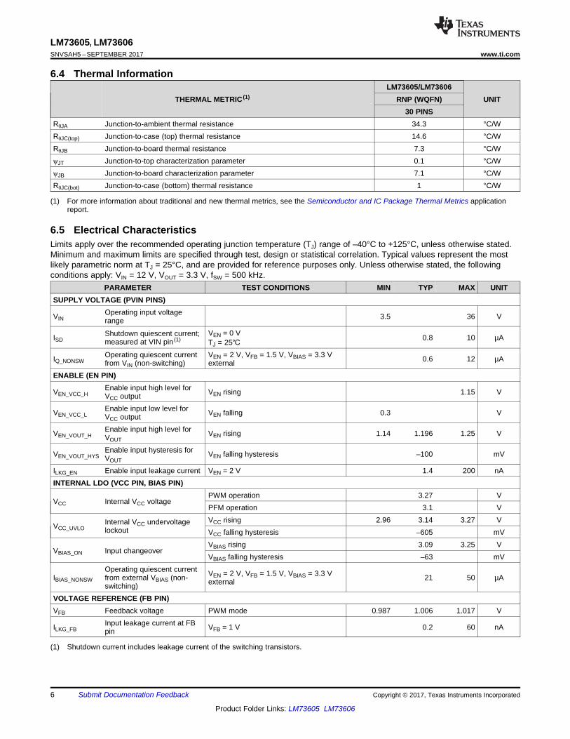
(1) For more information about traditional and new thermal metrics, see the Semiconductor and IC Package Thermal Metrics applicationreport.
6.4 Thermal Information
THERMAL METRIC (1)LM73605/LM73606
UNITRNP (WQFN)30 PINS
RθJA Junction-to-ambient thermal resistance 34.3 °C/WRθJC(top) Junction-to-case (top) thermal resistance 14.6 °C/WRθJB Junction-to-board thermal resistance 7.3 °C/WψJT Junction-to-top characterization parameter 0.1 °C/WψJB Junction-to-board characterization parameter 7.1 °C/WRθJC(bot) Junction-to-case (bottom) thermal resistance 1 °C/W
(1) Shutdown current includes leakage current of the switching transistors.
6.5 Electrical CharacteristicsLimits apply over the recommended operating junction temperature (TJ) range of –40°C to +125°C, unless otherwise stated.Minimum and maximum limits are specified through test, design or statistical correlation. Typical values represent the mostlikely parametric norm at TJ = 25°C, and are provided for reference purposes only. Unless otherwise stated, the followingconditions apply: VIN = 12 V, VOUT = 3.3 V, fSW = 500 kHz.
PARAMETER TEST CONDITIONS MIN TYP MAX UNITSUPPLY VOLTAGE (PVIN PINS)
VINOperating input voltagerange 3.5 36 V
ISDShutdown quiescent current;measured at VIN pin (1)
VEN = 0 VTJ = 25 0.8 10 µA
IQ_NONSWOperating quiescent currentfrom VIN (non-switching)
VEN = 2 V, VFB = 1.5 V, VBIAS = 3.3 Vexternal 0.6 12 µA
ENABLE (EN PIN)
VEN_VCC_HEnable input high level forVCC output VEN rising 1.15 V
VEN_VCC_LEnable input low level forVCC output VEN falling 0.3 V
VEN_VOUT_HEnable input high level forVOUT
VEN rising 1.14 1.196 1.25 V
VEN_VOUT_HYSEnable input hysteresis forVOUT
VEN falling hysteresis –100 mV
ILKG_EN Enable input leakage current VEN = 2 V 1.4 200 nAINTERNAL LDO (VCC PIN, BIAS PIN)
VCC Internal VCC voltagePWM operation 3.27 VPFM operation 3.1 V
VCC_UVLOInternal VCC undervoltagelockout
VCC rising 2.96 3.14 3.27 VVCC falling hysteresis –605 mV
VBIAS_ON Input changeoverVBIAS rising 3.09 3.25 VVBIAS falling hysteresis –63 mV
IBIAS_NONSW
Operating quiescent currentfrom external VBIAS (non-switching)
VEN = 2 V, VFB = 1.5 V, VBIAS = 3.3 Vexternal 21 50 µA
VOLTAGE REFERENCE (FB PIN)VFB Feedback voltage PWM mode 0.987 1.006 1.017 V
ILKG_FBInput leakage current at FBpin VFB = 1 V 0.2 60 nA
7
LM73605, LM73606www.ti.com SNVSAH5 –SEPTEMBER 2017
Product Folder Links: LM73605 LM73606
Submit Documentation FeedbackCopyright © 2017, Texas Instruments Incorporated
Electrical Characteristics (continued)Limits apply over the recommended operating junction temperature (TJ) range of –40°C to +125°C, unless otherwise stated.Minimum and maximum limits are specified through test, design or statistical correlation. Typical values represent the mostlikely parametric norm at TJ = 25°C, and are provided for reference purposes only. Unless otherwise stated, the followingconditions apply: VIN = 12 V, VOUT = 3.3 V, fSW = 500 kHz.
PARAMETER TEST CONDITIONS MIN TYP MAX UNIT
(2) This current limit was measured as the internal comparator trip point. Due to inherent delays in the current limit comparator and drivers,the peak current limit measured in closed loop with faster slew rate will be larger, and valley current limit will be lower.
(3) Measured at pins(4) Ensured by design
HIGH SIDE DRIVER (CBOOT PIN)
VCBOOT_UVLOCBOOT - SW undervoltagelockout 1.6 2.2 2.7 V
CURRENT LIMITS AND HICCUP
IHS_LIMITShort-circuit, high-sidecurrent limit (2)
LM73605 6 7.3 8.35A
LM73606 7.4 8.7 9.85
ILS_LIMIT Low-side current limit (2) LM73605 4.79 5.5 6.1A
LM73606 5.8 6.6 7.25
INEG_LIMIT Negative current limitLM73605 –5
ALM73606 –6
VHICCUP Hiccup threshold on FB pin 0.36 0.4 0.44 VIL_ZC Zero cross-current limit 0.06 ASOFT START (SS/TRK PIN)ISSC Soft-start charge current 1.8 2 2.2 µA
RSSDSoft-start dischargeresistance UVLO, TSD, OCP, or EN = 0 1 kΩ
POWER GOOD (PGOOD PIN) and OVERVOLTAGE PROTECTION
VPGOOD_OVPower-good overvoltagethreshold % of FB voltage 106% 110% 113%
VPGOOD_UVPower-good undervoltagethreshold % of FB voltage 86% 90% 93%
VPGOOD_HYS Power-good hysteresis % of FB voltage 1.2%
VPGOOD_VALIDMinimum input voltage forproper PGOOD function
50-µA pullup to PGOOD pin, VEN = 0 V,TJ = 25°C 1.3 2 V
RPGOOD Power-good ON-resistanceVEN = 2.5V 40 100
ΩVEN = 0 V 30 90
MOSFETS
RDS_ON_HS(3) High-side MOSFET ON-
resistance IOUT = 1 A, VBIAS = VOUT = 3.3 V 53 90 mΩ
RDS_ON_LS(3) Low-side MOSFET ON-
resistance IOUT = 1 A, VBIAS = VOUT = 3.3 V 31 55 mΩ
THERMAL SHUTDOWN
TSD(4) Thermal shutdown threshold Shutdown threshold 160 °C
Recovery threshold 135 °C
(1) Ensured by design
6.6 Timing CharacteristicsMIN NOM MAX UNIT
CURRENT LIMITS AND HICCUP
NOC(1) Number of switching cycles
before hiccup is tripped 128 Cycles
tOCOvercurrent hiccup retry delaytime 46 ms
8
LM73605, LM73606SNVSAH5 –SEPTEMBER 2017 www.ti.com
Product Folder Links: LM73605 LM73606
Submit Documentation Feedback Copyright © 2017, Texas Instruments Incorporated
Timing Characteristics (continued)MIN NOM MAX UNIT
SOFT START (SS/TRK PIN)
tSS Internal soft-start time CSS = OPEN, from EN risingedge to PGOOD rising edge 3.5 6.3 ms
POWER GOOD (PGOOD PIN) and OVERVOLTAGE PROTECTION
tPGOOD_RISEPGOOD rising edge deglitchdelay 80 140 200 µs
tPGOOD_FALLPGOOD falling edge deglitchdelay 80 140 200 µs
6.7 Switching CharacteristicsPARAMETER TEST CONDITIONS MIN TYP MAX UNIT
PWM LIMITS (SW PINS)tON-MIN Minimum switch on-time 60 82 nstOFF-MIN Minimum switch off-time 70 120 nstON-MAX Maximum switch on-time HS timeout in dropout 3 6 9 µsOSCILLATOR (RT and SYNC PINS)fOSC Internal oscillator frequency RT = Open 440 500 560 kHz
fADJ
Minimum adjustable frequency byRT or SYNC RT =115 kΩ, 0.1% 315 350 385 kHz
Maximum adjustable frequency byRT or SYNC RT = 17.4 kΩ, 0.1% 1980 2200 2420 kHz
VSYNC_HIGH Sync input high level threshold 2 VVSYNC_LOW Sync input low level threshold 0.4 V
VMODE_HIGHMode input high level threshold forFPWM 0.42 V
VMODE_LOWMode input low level threshold forAUTO mode 0.4 V
tSYNC_MINSync input minimum ON and OFF-time 80 ns
6.8 System CharacteristicsThe following specifications apply to the circuit found in typical schematic with appropriate modifications from typical bill ofmaterials. These parameters are not tested in production and represent typical performance only. Unless otherwise stated thefollowing conditions apply: TA = 25°C, VIN = 12 V, VOUT = 3.3 V, fSW = 500 kHz.
PARAMETER TEST CONDITIONS MIN TYP MAX UNIT
VFB_PFMOutput voltage offset at no loadin auto mode
VIN = 3.8 V to 36 V, VSYNC = 0 V, auto modeIOUT = 0 A 2%
VDROP
Minimum input to outputvoltage differential to maintainspecified accuracy
VOUT = 5 V, IOUT = 3 A, fSW = 2.2 MHz 0.4 V
IQ_SWOperating quiescent current(switching)
VEN = 3.3 V, IOUT = 0 A, RT = open, VBIAS =VOUT = 3.3 V , RFBT = 1 Meg 15 µA
IPEAK_MIN Minimum inductor peak current
LM73605:VSYNC = 0, IOUT = 10 mA 1
ALM73606:VSYNC = 0 V, IOUT = 10 mA 1.3
IBIAS_SWOperating quiescent currentfrom external VBIAS (switching)
fSW = 500 kHz, IOUT = 1 A 7 mAfSW = 2.2 MHz, IOUT = 1 A 25
DMAX Maximum switch duty cycle While in frequency foldback 97.5%
tDEADDead time between high-sideand low-side MOSFETs 4 ns
Temperature (°C)
Cur
rent
Lim
its (
A)
-40 -20 0 20 40 60 80 100 1206
6.6
7.2
7.8
8.4
9
CHAR
HSLS
Temperature (°C)
Fre
quen
cy (
kHz)
-40 -20 0 20 40 60 80 100 1200
250
500
750
1000
1250
1500
1750
2000
2250
2500
CHAR
FREQ = 350 kHzFREQ = 1 MHzFREQ = 2.2 MHz
VIN (V)
Fee
dbac
k V
olta
ge (
V)
3 6 9 12 15 18 21 24 27 30 33 361
1.001
1.002
1.003
1.004
1.005
1.006
1.007
1.008
1.009
1.01
CHAR
Temp = -40°CTemp = 25°CTemp = 125°C
Temperature (°C)
Cur
rent
Lim
its (
A)
-40 -20 0 20 40 60 80 100 1205
5.5
6
6.5
7
7.5
CHAR
HSLS
Temperature (°C)
RD
S-O
N (
m:
)
-40 -20 0 20 40 60 80 100 120 14020
25
30
35
40
45
50
55
60
65
70
75
CHAR
HS SwitchLS Switch
Temperature (°C)
Shu
tdow
n C
urre
nt (
nA)
-40 -20 0 20 40 60 80 100 120200300400500600700800900
1000110012001300140015001600
PlotPlotCHAR
VIN = 3.5 VVIN = 12 VVIN = 36 V
9
LM73605, LM73606www.ti.com SNVSAH5 –SEPTEMBER 2017
Product Folder Links: LM73605 LM73606
Submit Documentation FeedbackCopyright © 2017, Texas Instruments Incorporated
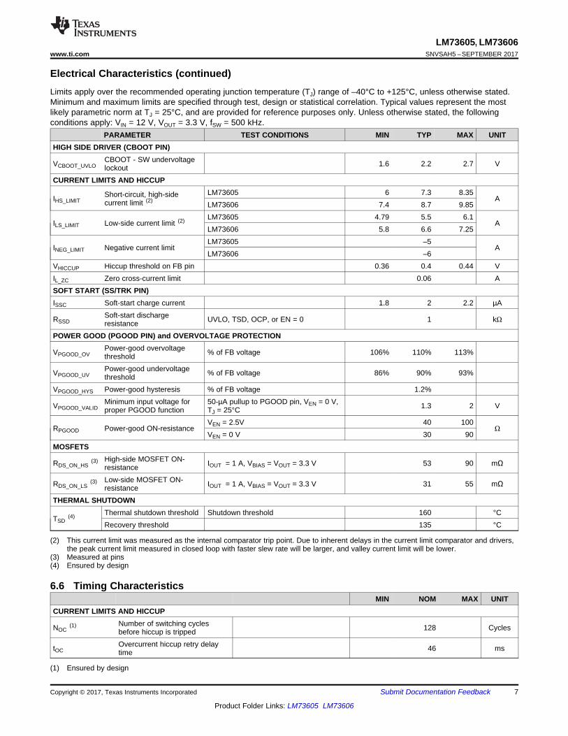
6.9 Typical CharacteristicsUnless otherwise specified, VIN = 12 V, VOUT = 3.3 V and fSW = 500 kHz. Curves represent most likely parametric norm atspecified condition.
Figure 1. High Side and Low Side Switches RDS-ON Figure 2. Shutdown Quiescent Current
Figure 3. Feedback Voltage Figure 4. LM73605 High Side and Low Side Current Limits
Figure 5. LM73606 High Side and Low Side Current Limit Figure 6. Switching Frequency Set by RT Resistor
Temperature (°C)
PG
OO
D T
hres
hold
s (%
)
-40 -20 0 20 40 60 80 100 12085
90
95
100
105
110
115
CHAR
OV TrippingOV RecoveryUV RecoveryUV Tripping
Temperature (°C)
Fre
quen
cy w
ith R
T P
in F
loat
ing
(kH
z)
-40 -20 0 20 40 60 80 100 120450
460
470
480
490
500
510
520
530
540
550
CHAR
VIN = 3.5 VVIN = 12 VVIN = 36 V
Temperature (°C)
Ena
ble
Thr
esho
lds
(V)
-40 -20 0 20 40 60 80 100 120 1400.56
0.64
0.72
0.8
0.88
0.96
1.04
1.12
1.2
1.28
CHAR
VEN_VOUT RisingVEN_VOUT FallingVEN_VCC RisingVEN_VCC Falling
10
LM73605, LM73606SNVSAH5 –SEPTEMBER 2017 www.ti.com
Product Folder Links: LM73605 LM73606
Submit Documentation Feedback Copyright © 2017, Texas Instruments Incorporated
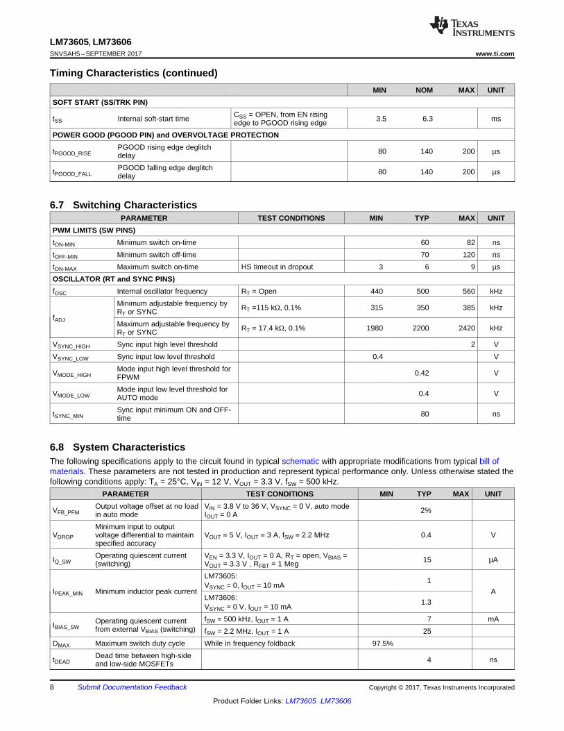
Typical Characteristics (continued)Unless otherwise specified, VIN = 12 V, VOUT = 3.3 V and fSW = 500 kHz. Curves represent most likely parametric norm atspecified condition.
Figure 7. Switching Frequency with RT Pin Open Circuit Figure 8. Enable Thresholds
Figure 9. PGOOD Thresholds
REF
PVIN
BIAS
PGOOD
ENABLE
CONTROL LOGIC
AGND
PGND
Oscillator
LDO
SYNC/MODE
VCC
SW
FB
HS I Sense
EA
RT
UVLO
Hiccup Detector
Internal SS
OV/UV Detector
+
PFM Detector
Slope Comp
+
±
PrecisionEnable
LS I Sense
PGood
FB
RC
CC
ISSC
+ ±
ICMD
ILIMIT
+±
VCC
CLK
FPWM
TSD
VBOOT
VBOOT
UVLO
SS/TRK
Copyright © 2017, Texas Instruments Incorporated
CBOOT
VSW
VSW
11
LM73605, LM73606www.ti.com SNVSAH5 –SEPTEMBER 2017
Product Folder Links: LM73605 LM73606
Submit Documentation FeedbackCopyright © 2017, Texas Instruments Incorporated
7 Detailed Description
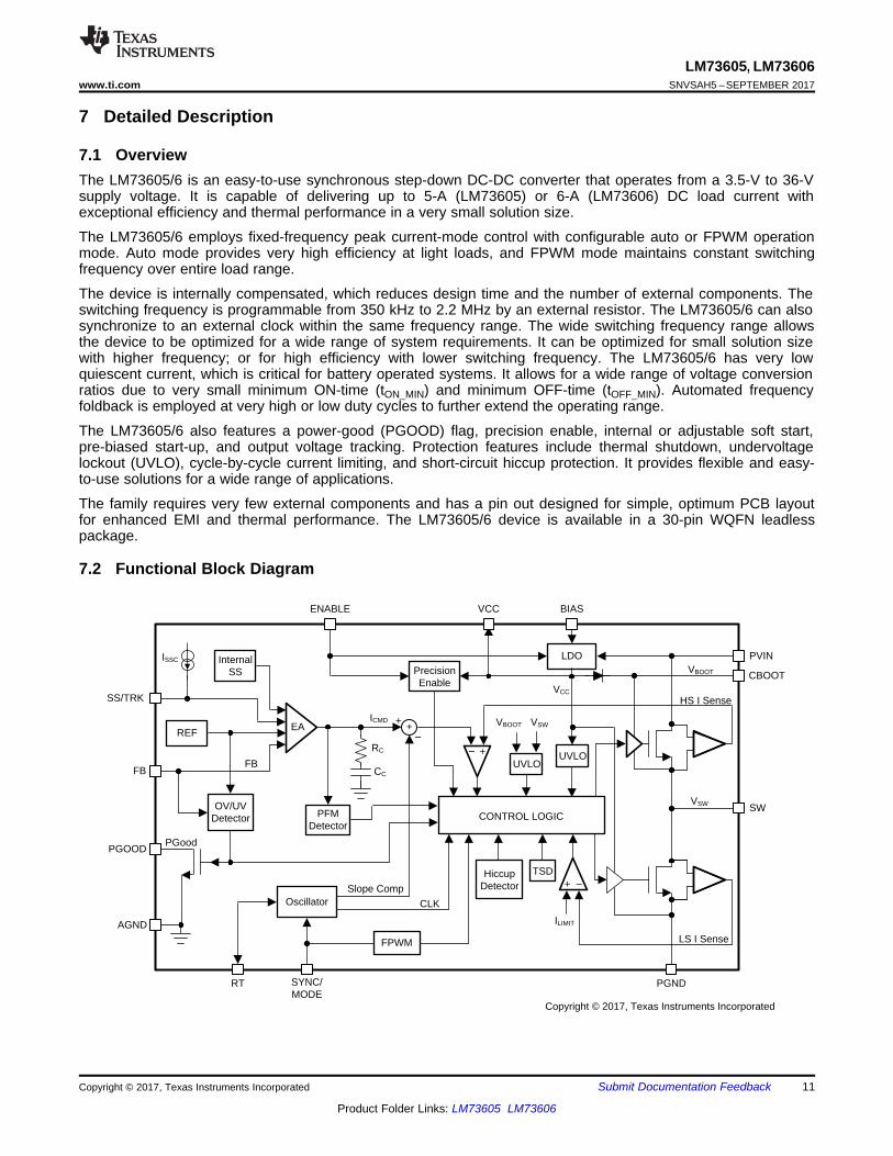
7.1 OverviewThe LM73605/6 is an easy-to-use synchronous step-down DC-DC converter that operates from a 3.5-V to 36-Vsupply voltage. It is capable of delivering up to 5-A (LM73605) or 6-A (LM73606) DC load current withexceptional efficiency and thermal performance in a very small solution size.
The LM73605/6 employs fixed-frequency peak current-mode control with configurable auto or FPWM operationmode. Auto mode provides very high efficiency at light loads, and FPWM mode maintains constant switchingfrequency over entire load range.
The device is internally compensated, which reduces design time and the number of external components. Theswitching frequency is programmable from 350 kHz to 2.2 MHz by an external resistor. The LM73605/6 can alsosynchronize to an external clock within the same frequency range. The wide switching frequency range allowsthe device to be optimized for a wide range of system requirements. It can be optimized for small solution sizewith higher frequency; or for high efficiency with lower switching frequency. The LM73605/6 has very lowquiescent current, which is critical for battery operated systems. It allows for a wide range of voltage conversionratios due to very small minimum ON-time (tON_MIN) and minimum OFF-time (tOFF_MIN). Automated frequencyfoldback is employed at very high or low duty cycles to further extend the operating range.
The LM73605/6 also features a power-good (PGOOD) flag, precision enable, internal or adjustable soft start,pre-biased start-up, and output voltage tracking. Protection features include thermal shutdown, undervoltagelockout (UVLO), cycle-by-cycle current limiting, and short-circuit hiccup protection. It provides flexible and easy-to-use solutions for a wide range of applications.
The family requires very few external components and has a pin out designed for simple, optimum PCB layoutfor enhanced EMI and thermal performance. The LM73605/6 device is available in a 30-pin WQFN leadlesspackage.
7.2 Functional Block Diagram
SWVIN
PGNDPGND
CIN
VIN
COUT
VOUTL
Synchronous Buck SWVIN
CIN
VIN
COUT
VOUTL
Non Synchronous Buck
Copyright © 2017, Texas Instruments Incorporated
12
LM73605, LM73606SNVSAH5 –SEPTEMBER 2017 www.ti.com
Product Folder Links: LM73605 LM73606
Submit Documentation Feedback Copyright © 2017, Texas Instruments Incorporated
7.3 Feature Description
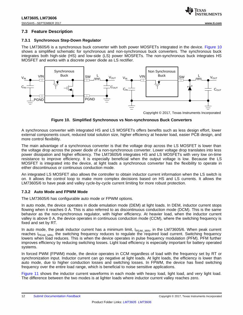
7.3.1 Synchronous Step-Down RegulatorThe LM73605/6 is a synchronous buck converter with both power MOSFETs integrated in the device. Figure 10shows a simplified schematic for synchronous and non-synchronous buck converters. The synchronous buckintegrates both high-side (HS) and low-side (LS) power MOSFETs. The non-synchronous buck integrates HSMOSFET and works with a discrete power diode as LS rectifier.
Figure 10. Simplified Synchronous vs Non-synchronous Buck Converters
A synchronous converter with integrated HS and LS MOSFETs offers benefits such as less design effort, lowerexternal components count, reduced total solution size, higher efficiency at heavier load, easier PCB design, andmore control flexibility.
The main advantage of a synchronous converter is that the voltage drop across the LS MOSFET is lower thanthe voltage drop across the power diode of a non-synchronous converter. Lower voltage drop translates into lesspower dissipation and higher efficiency. The LM73605/6 integrates HS and LS MOSFETs with very low on-timeresistance to improve efficiency. It is especially beneficial when the output voltage is low. Because the LSMOSFET is integrated into the device, at light loads a synchronous converter has the flexibility to operate ineither discontinuous or continuous conduction mode.
An integrated LS MOSFET also allows the controller to obtain inductor current information when the LS switch ison. It allows the control loop to make more complex decisions based on HS and LS currents. It allows theLM73605/6 to have peak and valley cycle-by-cycle current limiting for more robust protection.
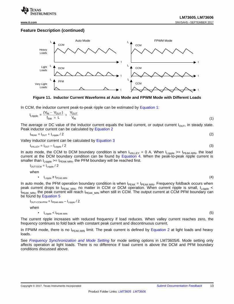
7.3.2 Auto Mode and FPWM ModeThe LM73605/6 has configurable auto mode or FPWM options.
In auto mode, the device operates in diode emulation mode (DEM) at light loads. In DEM, inductor current stopsflowing when it reaches 0 A. This is also referred to as discontinuous conduction mode (DCM). This is the samebehavior as the non-synchronous regulator, with higher efficiency. At heavier load, when the inductor currentvalley is above 0 A, the device operates in continuous conduction mode (CCM), where the switching frequency isfixed and set by RT.
In auto mode, the peak inductor current has a minimum limit, IPEAK_MIN, in the LM73605/6. When peak currentreaches IPEAK_MIN, the switching frequency reduces to regulate the required load current. Switching frequencylowers when load reduces. This is when the device operates in pulse frequency modulation (PFM). PFM furtherimproves efficiency by reducing switching losses. Light load efficiency is especially important for battery operatedsystems.
In forced PWM (FPWM) mode, the device operates in CCM regardless of load with the frequency set by RT orsynchronization input. Inductor current can go negative at light loads. At light loads, the efficiency is lower thanauto mode, due to higher conduction losses and switching losses. In FPWM, the device has fixed switchingfrequency over the entire load range, which is beneficial to noise sensitive applications.
Figure 11 shows the inductor current waveforms in each mode with heavy load, light load, and very light load.The difference between the two modes is at lighter loads where inductor current valley reaches zero.
u
u
IN OUT OUTLripple
SW IN
(V V ) VI =
f L V
IL
IL
t
t
t
IL
CCM
DCM
PFM
IL
tIL
t
CCM
Auto Mode FPWM Mode
IL
t
CCM
CCM
Heavy Loads
Light Loads
Very Light Loads
13
LM73605, LM73606www.ti.com SNVSAH5 –SEPTEMBER 2017
Product Folder Links: LM73605 LM73606
Submit Documentation FeedbackCopyright © 2017, Texas Instruments Incorporated
Feature Description (continued)
Figure 11. Inductor Current Waveforms at Auto Mode and FPWM Mode with Different Loads
In CCM, the inductor current peak-to-peak ripple can be estimated by Equation 1:
(1)
The average or DC value of the inductor current equals the load current, or output current IOUT, in steady state.Peak inductor current can be calculated by Equation 2
IPEAK = IOUT + ILripple / 2 (2)
Valley inductor current can be calculated by Equation 3IVALLEY = IOUT – ILripple / 2 (3)
In auto mode, the CCM to DCM boundary condition is when IVALLEY = 0 A. When ILripple >= IPEAK-MIN, the loadcurrent at the DCM boundary condition can be found by Equation 4. When the peak-to-peak ripple current issmaller than ILripple >= IPEAK-MIN, the PFM boundary will be reached first.
IOUT-DCM = ILripple / 2
when• ILripple ≥ IPEAK-MIN (4)
In auto mode, the PFM operation boundary condition is when IPEAK = IPEAK-MIN. Frequency foldback occurs whenpeak current drops to IPEAK_MIN, no matter in CCM or DCM operation. When current ripple is small, ILripple <IPEAK_MIN, the peak current will reach IPEAK_MIN when still in CCM. The output current at CCM PFM boundary canbe found by Equation 5
IOUT-CCM-PFM = IPEAK-MIN – ILripple / 2
when• ILripple < IPEAK-MIN (5)
The current ripple increases with reduced frequency if load reduces. When valley current reaches zero, thefrequency continues to fold back with constant peak current and discontinuous current.
In FPWM mode, there is no IPEAK-MIN limit. The peak current is defined by Equation 2 at light loads and heavyloads.
See Frequency Synchronization and Mode Setting for mode setting options in LM73605/6. Mode setting onlyaffects operation at light loads. There is no difference if load current is above the DCM and PFM boundaryconditions discussed above.
FB
RFBT
RFBB
VOUT
0
0
VIN
-VD
tON
t
t
Indu
ctor
Cur
rent
D = tON / TSW
VSW
TSWIL
SW
Vol
tage
IOUT
IL-PEAK
ILripple
IL-VALLEY
tOFF
14
LM73605, LM73606SNVSAH5 –SEPTEMBER 2017 www.ti.com
Product Folder Links: LM73605 LM73606
Submit Documentation Feedback Copyright © 2017, Texas Instruments Incorporated
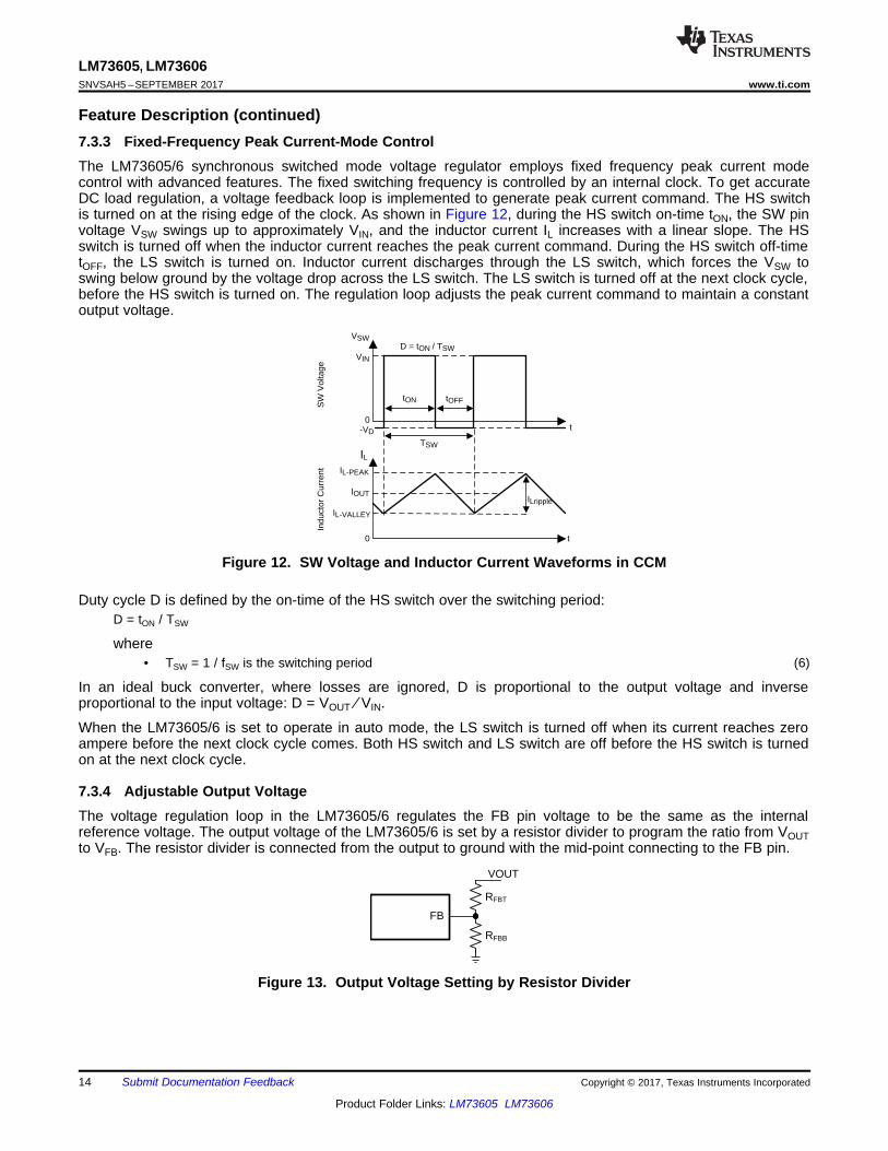
Feature Description (continued)7.3.3 Fixed-Frequency Peak Current-Mode ControlThe LM73605/6 synchronous switched mode voltage regulator employs fixed frequency peak current modecontrol with advanced features. The fixed switching frequency is controlled by an internal clock. To get accurateDC load regulation, a voltage feedback loop is implemented to generate peak current command. The HS switchis turned on at the rising edge of the clock. As shown in Figure 12, during the HS switch on-time tON, the SW pinvoltage VSW swings up to approximately VIN, and the inductor current IL increases with a linear slope. The HSswitch is turned off when the inductor current reaches the peak current command. During the HS switch off-timetOFF, the LS switch is turned on. Inductor current discharges through the LS switch, which forces the VSW toswing below ground by the voltage drop across the LS switch. The LS switch is turned off at the next clock cycle,before the HS switch is turned on. The regulation loop adjusts the peak current command to maintain a constantoutput voltage.
Figure 12. SW Voltage and Inductor Current Waveforms in CCM
Duty cycle D is defined by the on-time of the HS switch over the switching period:D = tON / TSW
where• TSW = 1 / fSW is the switching period (6)
In an ideal buck converter, where losses are ignored, D is proportional to the output voltage and inverseproportional to the input voltage: D = VOUT ⁄ VIN.
When the LM73605/6 is set to operate in auto mode, the LS switch is turned off when its current reaches zeroampere before the next clock cycle comes. Both HS switch and LS switch are off before the HS switch is turnedon at the next clock cycle.
7.3.4 Adjustable Output VoltageThe voltage regulation loop in the LM73605/6 regulates the FB pin voltage to be the same as the internalreference voltage. The output voltage of the LM73605/6 is set by a resistor divider to program the ratio from VOUTto VFB. The resistor divider is connected from the output to ground with the mid-point connecting to the FB pin.
Figure 13. Output Voltage Setting by Resistor Divider
u u
ON_MAXOUT _MAX IN_MIN OUT DS_ON_HS
ON_MAX OFF_MIN
tV V I (R DCR)
t t
FBFBB FBT
OUT FB
VR R
V V
15
LM73605, LM73606www.ti.com SNVSAH5 –SEPTEMBER 2017
Product Folder Links: LM73605 LM73606
Submit Documentation FeedbackCopyright © 2017, Texas Instruments Incorporated
Feature Description (continued)The internal voltage reference and feedback loop produce precise voltage regulation over temperature. TIrecommends using divider resistors with 1% tolerance or better, and with temperature coefficient of 100 ppm orlower. Typically, RFBT = 10 kΩ to 100 kΩ is recommended. Larger RFBT and RFBB values reduce the quiescentcurrent going through the divider, which help maintain high efficiency at very light load. But larger divider valuesalso make the feedback path more susceptible to noise. If efficiency at very light load is critical in a certainapplication, RFBT up to 1 MΩ can be used.
RFBB can be calculated by Equation 7:
(7)
The minimum programmable VOUT equals VFB, with RFBB open. The maximum VOUT is limited by the maximumduty cycle at a given frequency:
DMAX = 1 – (tOFF_MIN / TSW)
where• tOFF_MIN is the minimum off time of the HS switch• TSW = 1 / fSW is the switching period (8)
Ideally, without frequency foldback, VOUT_MAX = VIN_MIN × DMAX.
Power losses in the circuit reduces the maximum output voltage. The LM73605/6 folds back switching frequencyunder tOFF_MIN condition to further extend VOUT_MAX. The device maintains output regulation with lower inputvoltage. The minimum fold-back frequency is limited by the maximum HS on-time, tON_MAX. Maximum outputvoltage with frequency foldback can be estimated by:
(9)
The voltage drops on the HS MOSFET and inductor DCR have been taken into account in Equation 9. Theswitching losses were not included.
If the resistor divider is not connected properly, the output voltage cannot be regulated because the feedbackloop cannot obtain correct output voltage information. If the FB pin is shorted to ground or disconnected, theoutput voltage is driven close to VIN. The load connected to the output could be damaged under this condition.Do not short FB to ground or leave it open circuit during operation.
The FB pin is a noise sensitive node. It is important to place the resistor divider as close as possible to the FBpin, and route the feedback node with a short and thin trace. The trace connecting VOUT to RFBT can be long, butit must be routed away from the noisy area of the PCB. For more layout recommendations, see Layout.
7.3.5 Enable and UVLOThe LM73605/6 regulates output voltage when the VCC voltage is higher than the undervoltage lock out (UVLO)level, VCC_UVLO, and the EN voltage is higher than VEN_VOUT_H.
The internal LDO output voltage VCC is turned on when the EN voltage is higher than VEN_VCC_H. The precisionenable circuitry is also turned on when VCC is above UVLO. Normal operation of the LM73605/6 with regulatedoutput voltage is enabled when the EN voltage is greater than VEN_VOUT_H. When the EN voltage is less thanVEN_VCC_L, the device is in shutdown mode. The internal dividers make sure VEN_VOUT_H is always higher thanVEN_VCC_H.
The EN pin cannot be left floating. The simplest way to enable the operation of the LM73605/6 is to connect theEN pin to PVIN, which allows self-start-up of the LM73605/6 when VIN rises. Use of a pullup resistor betweenPVIN and EN pins helps reduce noise coupling from PVIN pin to the EN pin.
Many applications benefit from employing an enable divider to establish a customized system UVLO. This can beused either for sequencing, system timing requirement, or to reduce the occurrence of deep discharge of abattery power source. Figure 14 shows how to use a resistor divider to set a system UVLO level. An externallogic output can also be used to drive the EN pin for system sequencing.
EN_ VOUT _HENB ENT
IN_ ON_H EN_VOUT_H
VR = R
V V
VIN
ENABLE
RENT
RENB
16
LM73605, LM73606SNVSAH5 –SEPTEMBER 2017 www.ti.com
Product Folder Links: LM73605 LM73606
Submit Documentation Feedback Copyright © 2017, Texas Instruments Incorporated
Feature Description (continued)
Figure 14. System UVLO
With a selected RENT, the RENB can be calculated by:
where• VIN_ON_H is the desired supply voltage threshold to turn on this device (10)
Note that the divider adds to supply quiescent current by VIN / (RENT + RENB). Small RENT and RENB values addmore quiescent current loss. However, large divider values make the node more sensitive to noise. RENT in thehundreds of kΩ range is a good starting point.
7.3.6 Internal LDO, VCC_UVLO, and BIAS InputThe LM73605/6 integrates an internal LDO, generating VCC voltage for control circuitry and MOSFET drivers.The VCC pin must have a 1-µF to 4.7-µF bypass capacitor placed as close as possible to the pin and properlygrounded. Do not load the VCC pin or short it to ground during operation. Shorting VCC pin to ground duringoperation may damage the device.
The UVLO on VCC voltage, VCC_UVLO, turns off the regulation when VCC voltage is too low. It prevents theLM73605/6 from operating until the VCC voltage is enough for the internal circuitry. Hysteresis on VCC_UVLOprevents the part from turning off during power up if VIN droops due to input current demands. The LDOgenerates VCC voltage from one of the two inputs: the supply voltage VIN, or the BIAS input. When BIAS is tiedto ground, the LDO input is VIN. When BIAS is tied to a voltage higher than 3.3 V, the LDO input is VBIAS. BIASvoltage must be lower than both VIN and 18 V.
The BIAS input is designed to reduce the LDO power loss. The LDO power loss is:PLOSS_LDO = ILDO × (VIN_LDO – VOUT_LDO) (11)
The higher the difference between the input and output voltages of the LDO, the more loss occurs to supply thesame LDO output current. The BIAS input provides an option to supply the LDO with a lower voltage than VIN, toreduce the difference of the input and output voltages of the LDO and reduce power loss. For example, if theLDO current is 10 mA at a certain frequency with VIN = 24 V and VOUT = 5 V. The LDO loss with BIAS tied toground is equal to 10 mA × (24 V – 3.27 V) = 207.3 mW, while the loss with BIAS tied to VOUT is equal to 10 mA× (5 – 3.27) = 17.3 mW.
The efficiency improvement is more significant at light and mid loads because the LDO loss is a higherpercentage in the total loss. The improvements is more significant with higher switching frequency because theLDO current is higher at higher switching frequency. The improvement is more significant when VIN » VOUTbecause the voltage difference is higher.
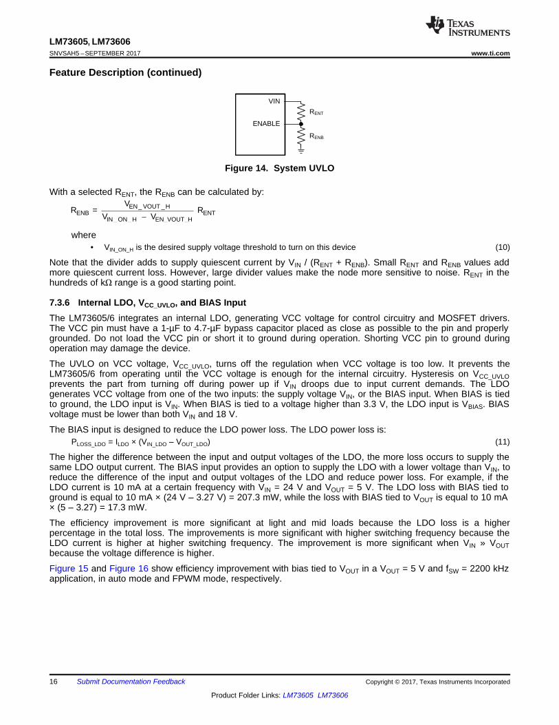
Figure 15 and Figure 16 show efficiency improvement with bias tied to VOUT in a VOUT = 5 V and fSW = 2200 kHzapplication, in auto mode and FPWM mode, respectively.
Load Current (A)
VC
C (
V)
0.001 0.01 0.02 0.05 0.1 0.2 0.5 1 2 3 4 552
2.12.22.32.42.52.62.72.82.9
33.13.23.33.43.5
VCC_
Auto ModeFPWM Mode
Load Current (A)
Effi
cien
cy (
%)
0.001 0.01 0.02 0.05 0.1 0.2 0.5 1 2 3 4 563035404550556065707580859095
100
EFF_
VIN = 12 V BIAS = VOUTVIN = 12 V BIAS = GNDVIN = 24 V BIAS = VOUTVIN = 24 V BIAS = GND
Load Current (A)
Effi
cien
cy (
%)
0.001 0.010.02 0.05 0.1 0.2 0.5 1 2 3 45 7 100
20
40
60
80
100
EFF_
VIN = 12 V BIAS = VOUTVIN = 12 V BIAS = GNDVIN = 24 V BIAS = VOUTVIN = 24 V BIAS = GND
17
LM73605, LM73606www.ti.com SNVSAH5 –SEPTEMBER 2017
Product Folder Links: LM73605 LM73606
Submit Documentation FeedbackCopyright © 2017, Texas Instruments Incorporated
Feature Description (continued)
VOUT = 5 V fSW = 2200 kHz Auto Mode
Figure 15. LM73606 Efficiency Comparison with Bias =VOUT to Bias = GND in Auto Mode
VOUT = 5 V fSW = 2200 kHz FPWM Mode
Figure 16. LM73606 Efficiency Comparison with Bias =VOUT to Bias = GND in FPWM Mode
TI recommends tying the BIAS pin to VOUT when VOUT is equal to or greater than 3.3 V and no greater than 18 V.Tie the BIAS pin to ground when not in use. A ceramic capacitor, CBIAS, can be used from the BIAS pin to groundfor bypassing. If VOUT has high frequency noise or spikes during transients or fault conditions, a resistor (1 to 10Ω) connected between VOUT to BIAS can be used together with CBIAS for filtering.
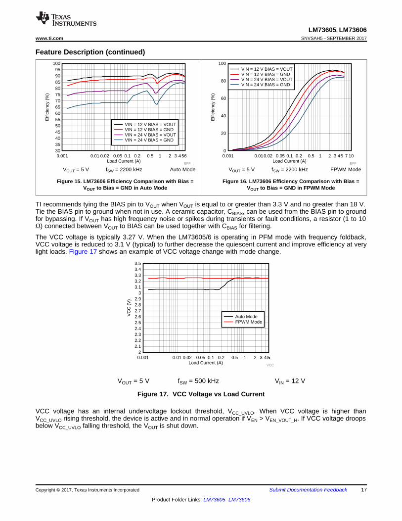
The VCC voltage is typically 3.27 V. When the LM73605/6 is operating in PFM mode with frequency foldback,VCC voltage is reduced to 3.1 V (typical) to further decrease the quiescent current and improve efficiency at verylight loads. Figure 17 shows an example of VCC voltage change with mode change.
VOUT = 5 V fSW = 500 kHz VIN = 12 V
Figure 17. VCC Voltage vs Load Current
VCC voltage has an internal undervoltage lockout threshold, VCC_UVLO. When VCC voltage is higher thanVCC_UVLO rising threshold, the device is active and in normal operation if VEN > VEN_VOUT_H. If VCC voltage droopsbelow VCC_UVLO falling threshold, the VOUT is shut down.
Enable
Internal SS Ramp
Ext Tracking Signal to SS pin
VOUT
SS/TRK
RTRT
RTRB
EXT RAMP
18
LM73605, LM73606SNVSAH5 –SEPTEMBER 2017 www.ti.com
Product Folder Links: LM73605 LM73606
Submit Documentation Feedback Copyright © 2017, Texas Instruments Incorporated
Feature Description (continued)7.3.7 Soft Start and Voltage TrackingThe LM73605/6 features controlled output voltage ramp during start-up. The soft-start feature reduces inrushcurrent during start-up and improves system performance and reliability.
If the SS/TRK pin is floating, the LM73605/6 starts up following the fixed internal soft-start ramp.
If longer soft-start time is desired, an external capacitor can be added from SS/TRK pin to ground. There is a 2-µA (typical) internal current source, ISSC, to charge the external capacitor. For a desired soft-start time tSS,capacitance of CSS can be found by Equation 12.
CSS = ISSC × tSS
where• CSS = soft-start capacitor value (F)• ISSC = soft-start charging current (A)• tSS = desired soft-start time (s) (12)
The FB voltage always follows the lower potential of the internal voltage ramp or the voltage on the SS/TRK pin.Thus, the soft-start time can only be extended longer than the internal soft-start time by connecting CSS. Use CSSto extend soft-start time when there are a large amount of output capacitors, or the output voltage is high, or theoutput is heavily loaded during start-up.
LM73605/6 is operating in diode emulation mode during start-up regardless of mode setting. The device iscapable of starting up into pre-biased output conditions. During start-up, the device sets the minimum inductorcurrent to zero to avoid back charging the input capacitors.
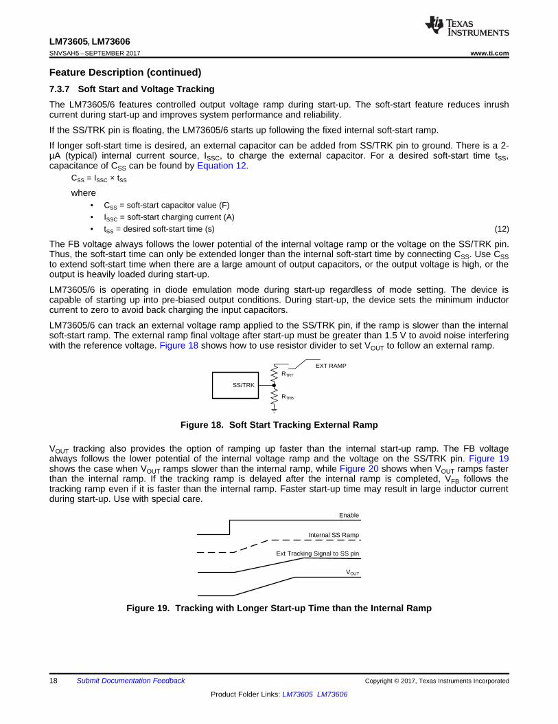
LM73605/6 can track an external voltage ramp applied to the SS/TRK pin, if the ramp is slower than the internalsoft-start ramp. The external ramp final voltage after start-up must be greater than 1.5 V to avoid noise interferingwith the reference voltage. Figure 18 shows how to use resistor divider to set VOUT to follow an external ramp.
Figure 18. Soft Start Tracking External Ramp
VOUT tracking also provides the option of ramping up faster than the internal start-up ramp. The FB voltagealways follows the lower potential of the internal voltage ramp and the voltage on the SS/TRK pin. Figure 19shows the case when VOUT ramps slower than the internal ramp, while Figure 20 shows when VOUT ramps fasterthan the internal ramp. If the tracking ramp is delayed after the internal ramp is completed, VFB follows thetracking ramp even if it is faster than the internal ramp. Faster start-up time may result in large inductor currentduring start-up. Use with special care.
Figure 19. Tracking with Longer Start-up Time than the Internal Ramp
Frequency (kHz)
RT
(k:
)
200 400 600 800 1000 1200 1400 1600 1800 2000 220010
20
30
40
50
60
70
80
90
100
110
120
RT_F
:
u u T -5
SW
1R (k ) =
f (kHz) 2.675 10 0.0007
Enable
Internal SS Ramp
Ext Tracking Signal to SS pin
VOUT
19
LM73605, LM73606www.ti.com SNVSAH5 –SEPTEMBER 2017
Product Folder Links: LM73605 LM73606
Submit Documentation FeedbackCopyright © 2017, Texas Instruments Incorporated
Feature Description (continued)
Figure 20. Tracking with Shorter Start-up Time than the Internal Ramp
The SS/TRK pin is discharged to ground by an internal pulldown resistor RSSD when the output voltage isshutting down, such as in the event of UVLO, thermal shutdown, hiccup, or VEN = 0. If a large CSS is used, andthe time when VEN = 0 V is very short, the CSS may not be fully discharged before the next soft start. Under thiscondition, the FB voltage follows the internal ramp slew rate until the voltage on CSS is reached, then follow theslew rate defined by CSS.
7.3.8 Adjustable Switching FrequencyThe internal oscillator frequency is controlled by the impedance on the RT pin. If the RT pin is open circuit, theLM73605/6 operates at its default switching frequency, 500 kHz. The RT pin is not designed to be connecteddirectly to ground. To program the switching frequency by RT resistor, Equation 13, or Figure 21, or Table 1 canbe used to find the resistance value.
(13)
Figure 21. RT Resistance vs Switching Frequency
Table 1. Typical Frequency Setting ResistanceSWITCHING FREQUENCY fSW (kHz) RT RESISTANCE (kΩ)
350 115400 100500 78.7 (or open)750 52.31000 39.21500 26.12000 19.12200 17.4
SYNC/MODE
RSYNC
EXT CLOCK
20
LM73605, LM73606SNVSAH5 –SEPTEMBER 2017 www.ti.com
Product Folder Links: LM73605 LM73606
Submit Documentation Feedback Copyright © 2017, Texas Instruments Incorporated
The choice of switching frequency is usually a compromise between conversion efficiency and the size of thesolution. Lower switching frequency has lower switching losses (including gate charge losses, switch transitionlosses, etc.). It usually results in higher overall efficiency. However, higher switching frequency allows the use ofsmaller power inductor and output capacitors, hence a more compact design. Lower inductance also helpstransient response (higher large signal slew rate of inductor current), and has lower DCR. The optimal switchingfrequency is usually a trade-off in a given application and thus needs to be determined on a case-by-case basis.Factors that need to be taken into account include input voltage range, output voltage, most frequent load currentlevel(s), external component choices, solution size/cost requirements, efficiency and thermal managementrequirements.
The choice of switching frequency may also be limited whether an operating condition triggers tON_MIN or tOFF_MIN.Minimum on-time, tON_MIN, is the smallest time that the HS switch can be on. Minimum OFF-time, tOFF_MIN, is thesmallest duration that the HS switch can be off.
In CCM operation, tON_MIN and tOFF_MIN limits the voltage conversion range given a selected switching frequency,FSW. The minimum duty cycle allowed is:
DMIN = tON_MIN × fSW (14)
The maximum duty cycle allowed is:DMAX = 1 – tOFF_MIN × fSW (15)
Given an output voltage, the choice of the switching frequency affects the allowed input voltage range, solutionsize and efficiency. The maximum operational supply voltage can be found by:
VIN-MAX = VOUT / (fSW × tON_MIN) (16)
At lower supply voltage, the switching frequency decreases once tOFF_MIN is tripped. The minimum VIN withoutfrequency foldback can be approximated by:
VIN-MIN = VOUT / (1 – fSW × tOFF_MIN) (17)
With a desired VOUT, the range of allowed VIN is narrower with higher switching frequency.
LM73605/6 has an advanced frequency fold-back algorithm under both tON_MIN and tOFF_MIN conditions. Withfrequency foldback, stable output voltage regulation is extended to wider range of supply voltages.
At very high VIN conditions, where tON_MIN limitation is met, the switching frequency reduces to allow higher VINwhile maintaining VOUT regulation. Note that the peak to peak inductor current ripple will increase with higher VINand lower frequency. TI does not recommend designing the circuit to operate with tON_MIN under typicalconditions.
At very low VIN conditions, where tOFF_MIN limitation is met, the switching frequency decreases until tON_MAXcondition is met. Such frequency fold-back mechanism allows the LM73605/6 to have very low dropout voltageregardless of frequency setting.
7.3.9 Frequency Synchronization and Mode SettingThe LM73605/6 switching action can synchronize to an external clock from 350 kHz to 2.2 MHz. TI recommendsconnecting the external clock to the SYNC/MODE pin with an appropriate termination resistor. Ground theSYNC/MODE pin if not used.
Figure 22. Frequency Synchronization
Recommendations for the external clock include a high level no lower than 2 V, low level no higher than 0.4 V,duty cycle between 10% and 90%, and both positive and negative pulse width no shorter than 80 ns. When theexternal clock fails at logic high or low, the LM73605/6 switches at the frequency programmed by the RT resistorafter a time-out period. TI recommends connecting a resistor to the RT pin such that the internal oscillatorfrequency is the same as the external clock frequency. This allows the regulator to continue operating atapproximately the same switching frequency if the external clock fails with the same control loop behavior.
FB
RFBT
RFBB
CFF
VOUT
uX
OUT OUT
Kf =
V C
21
LM73605, LM73606www.ti.com SNVSAH5 –SEPTEMBER 2017
Product Folder Links: LM73605 LM73606
Submit Documentation FeedbackCopyright © 2017, Texas Instruments Incorporated
The SYNC/MODE pin is also used as an operation mode control input.• To set the operation in auto mode, connect SYNC/MODE pin to ground, or a logic signal lower than 0.3 V.• To set the operation in FPWM mode, connect SYNC/MODE pin to a bias voltage or logic signal greater than
0.6 V.• When the LM73605/6 is synchronized to an external clock, the operation mode is FPWM.Table 2 summarizes the operation mode and features according to the SYNC/MODE input signal. For moredetails, see Active Mode and Auto Mode and FPWM Mode.
Table 2. SYNC/MODE Pin Settings and Operation ModesSYNC/MODE
INPUTSWITCHINGFREQUENCY
OPERATINGMODE
LIGHT LOAD BEHAVIOR
Logic low Set by RT resistor Auto mode
• No negative inductor current, device operates in discontinuous conduction mode(DCM) when current valley reaches 0 A.
• Minimum peak inductor current is limited at IPEAK-MIN; device operates in pulsefrequency modulation (PFM) mode when peak current reaches IPEAK-MIN.
• Switching frequency reduces in PFM mode.Logic high Set by RT resistor
FPWM mode• Fixed frequency continuous conduction mode (CCM) regardless of load• Inductor current have negative portion at light loads• No IPEAK-MIN
External clock Set by externalclock
7.3.10 Internal Compensation and CFF
The LM73605/6 is internally compensated. The internal compensation is designed such that the loop response isstable over a wide operating frequency and output voltage range. The internal R-C values are 500 kΩ and 30 pFrespectively.
When large resistance value (MΩ) is used for RFBT, the pole formed by an internal parasitic capacitor and RFBTcan be low enough to reduce the phase margin. If only low ESR output capacitors (ceramic types) are used forCOUT, the control loop could have low phase margin. To provide a phase boost an external feed-forwardcapacitor (CFF) can be added in parallel with RFBT. Choose the CFF capacitor to provide most phase boost at theestimated crossover frequency fX:
where• K = 20.27 with LM73605• K = 24.16 with LM73606 (18)
Select COUT so that the fX is no higher than 1/6 of the switching frequency. Typically, fX / fSW = 1/10 to 1/8provides a good combination of stability and performance.
Place the external feed-forward capacitor in parallel with the top resistor divider RFBT when additional phaseboost is needed.
Figure 23. Feed-Forward Capacitor for Loop Compensation
The feed-forward capacitor CFF in parallel with RFBT places an additional zero before the crossover frequency ofthe control loop to boost phase margin. The zero frequency can be found by Equation 19:
fZ-CFF = 1 / (2π × RFBT × CFF) (19)
An additional pole is also introduced with CFF at the frequency of:fP-CFF = 1 / (2π × CFF × (RFBT // RFBB)) (20)
PGPGB PGT
PU PG
VR = R
V V
VPU
RPGT
RPGB
PGOOD
FFx FBT FBT FBB
1 1C =
2 f R (R // R ) u
u S u u
22
LM73605, LM73606SNVSAH5 –SEPTEMBER 2017 www.ti.com
Product Folder Links: LM73605 LM73606
Submit Documentation Feedback Copyright © 2017, Texas Instruments Incorporated
Select the CFF so that the bandwidth of the control loop without the CFF is centered between fZ-CFF and fP-CFF. Thezero at fZ-CFF adds phase boost at the crossover frequency and improves transient response. The pole at fP-CFFhelps maintaining proper gain margin at frequency beyond the crossover.
The need of CFF depends on RFBT and COUT. Typically, choose RFBT ≤ 100 kΩ. CFF may not be required, becausethe internal parasitic pole is at higher frequency. If COUT has larger ESR, and ESR zero fZ-ESR = 1 / (2π × ESR ×COUT) is low enough to provide phase boost around the crossover frequency, do not use CFF. Equation 21 wastested for ceramic output capacitors:
(21)
The CFF creates a time constant with RFBT that couples in the attenuated output voltage ripple to the FB node. Ifthe CFF value is too large, it can couple too much ripple to the FB and affect VOUT regulation. It could also coupletoo much transient voltage deviation and falsely trigger PGOOD flag.
7.3.11 Bootstrap Capacitor and VBOOT-UVLO
The driver of the HS switch requires a bias voltage higher than the VIN voltage. The capacitor, CBOOT in SimplifiedSchematic, connected between CBOOT and SW pins works as a charge pump to boost voltage on the CBOOTpin to (VSW + VCC). A boot diode is integrated on the die to minimize external component count. TI recommendsa high-quality 0.47-µF, 6.3-V or higher voltage ceramic capacitor for CBOOT. The VBOOT_UVLO threshold is designedto maintain proper HS switch operation. If the CBOOT is not charged above this voltage with respect to SW, thedevice initiates a charging sequence using the LS switch before turning on the HS switch.
7.3.12 Power-Good and Overvoltage ProtectionThe LM73605/6 has a built-in power-good (PGOOD) flag to indicate whether the output voltage is at anappropriate level or not. The PGOOD flag can be used for start-up sequencing of multiple rails. The PGOOD pinis an open-drain output that requires a pullup resistor to an appropriate logic voltage (any voltage below 15 V).The pin can sink 5 mA of current and maintain its specified logic low level. A typical pullup resistor value is 10 kΩto 100 kΩ. When the FB voltage is higher than VPGOOD-OV or lower than VPGOOD-UV threshold, the PGOOD internalswitch is turned on, and the PGOOD pin voltage is pulled low. When the FB is within the range, the PGOODswitch is turned off, and the pin is pulled up to the voltage connected to the pullup resistor. The PGOOD functionalso have a deglitch timer for about 140 µs for each transition. If it is desired to pull up PGOOD pin to a voltagehigher than 15 V, a resistor divider can be used to divide the voltage down.
Figure 24. Divider for PGOOD Pullup Voltage
With a given pullup voltage VPU, select a desired voltage on the PGOOD pin, VPG. With a selected RPGT, theRPGB can be found by:
(22)
When the device is disabled, the output voltage is low, and the PGOOD flag indicates logic low as long as VIN >2 V.
23
LM73605, LM73606www.ti.com SNVSAH5 –SEPTEMBER 2017
Product Folder Links: LM73605 LM73606
Submit Documentation FeedbackCopyright © 2017, Texas Instruments Incorporated
7.3.13 Overcurrent and Short-Circuit ProtectionThe LM73605/6 is protected from overcurrent conditions with cycle-by-cycle current limiting on both HS and LSMOSFETs.
The HS switch is turned off when HS current goes beyond the peak current limit, IHS-LIMIT. The LS switch can onlybe turned off when LS current is below LS current limit, ILS-LIMIT. If the LS switch current is higher than ILS-LIMIT atthe end of a switching cycle, the switching cycle is extended until the LS current reduces below the limit.
Current limiting on both HS and LS switches provides tighter control of the maximum DC inductor current, oroutput current. They also help prevent runaway current at extreme conditions. With LM73605/6, the maximumoutput current is always limited at
IDC_LIMIT = (IHS_LIMIT + ILS_LIMIT) / 2 (23)
The LM73605/6 employs hiccup current protection at extreme overload conditions, including short-circuitcondition. Hiccup is only activated when VOUT droops below 40% (typical) of the regulation voltage and staysbelow for 128 consecutive switching cycles. Under overcurrent conditions when VOUT has not fallen below 40% ofregulation, the LM73605/6 continues operation with cycle-by-cycle HS and LS current limiting.
Hiccup is disabled during soft-start. When hiccup is triggered, the device turns off VOUT regulation and re-triessoft start after a re-try delay time, TOC = 46 ms (typical). The long wait time allows the device, and the load, tocool down under such fault conditions. If the fault condition still exists when re-try, hiccup shuts down the deviceand repeats the wait and re-try cycle. If the fault condition has been removed, the device starts up normally.
If tracking was used for initial sequencing, the device restarts using the internal soft-start ramp. Hiccup modehelps to reduce the device power dissipation and die temperature under severe overcurrent conditions and shortcircuits. It improves system reliability and prolongs the life span of the device.
In FPWM mode, negative current protection is implemented to protect the switches from extreme negativecurrents. When LS switch current reaches INEG-LIMIT, LS switch turns off, and HS switch turns on to conduct thenegative current. HS switch is turned off once its current reaches 0 A.
7.3.14 Thermal ShutdownThermal shutdown protection prevents the device from extreme junction temperature. The device is turned offwhen the junction temperature exceeds 160°C (typical). After thermal shutdown occurs, hysteresis prevents thedevice from switching until the junction temperature drops to approximately 135°C. When the junctiontemperature falls below 135°C, the LM73605/6 restarts.
7.4 Device Functional Modes
7.4.1 Shutdown ModeThe EN pin provides electrical on/off control of the device. When the EN pin voltage is below VEN_VCC_L, thedevice is in shutdown mode. The LDO output voltage VCC = 0 V and the output voltage VOUT = 0 V. In shutdownmode the quiescent current drops to a very low value.
7.4.2 Standby ModeThe internal LDO has a lower EN threshold than that required to start the regulator. When the EN pin voltage isabove VEN_VCC_H, the internal LDO regulates the VCC voltage. The precision enable circuitry is turned on onceVCC is above VCC_UVLO. The device is in standby mode if EN voltage is below VEN_VOUT_H. The internal MOSFETsremains in tri-state unless the voltage on EN pin goes beyond VEN_VOUT_H threshold. The LM73605/6 alsoemploys UVLO protection. If the VCC voltage is below the VCC_UVLO level, the output of the regulator is turnedoff.
7.4.3 Active ModeThe LM73605/6 is in active mode when the EN voltage is above VEN_VOUT_H, and VCC is above VCC_UVLO. Thesimplest way to enable the operation of the LM73605/6 is to pull up the EN pin to PVIN which allows self-start-upwhen the input voltage ramps up.
In active mode, depending on the load current and mode setting, the LM73605/6 is in one of four modes:1. CCM with fixed switching frequency when load current is above half of the peak-to-peak inductor current
ripple;
24
LM73605, LM73606SNVSAH5 –SEPTEMBER 2017 www.ti.com
Product Folder Links: LM73605 LM73606
Submit Documentation Feedback Copyright © 2017, Texas Instruments Incorporated
Device Functional Modes (continued)2. DCM with fixed switching frequency when load current is lower than half of the peak-to-peak inductor current
ripple in CCM operation;3. PFM when switching frequency is decreased at very light load;4. Under overcurrent or overtemperature conditions, the device operates in one of the fault protection modes.
Please refer to Table 2 for mode-setting details.
7.4.3.1 CCM ModeIn continuous conduction mode (CCM) operation, inductor current has a continuous triangular waveform. The HSswitch is on at the beginning of a switching cycle and the LS switch is turned off the end of each switching cycle.In auto mode, the LM73605/6 operates in CCM when the load current is higher than ½ of the peak-to-peakinductor current (ILripple). In FPWM mode, the LM73605/6 operates in CCM regardless of load.
In CCM operation, the switching frequency is typically constant, unless tON_MIN, tOFF_MIN, or IPEAK-MIN conditionsare met. The constant switching frequency is determined by RT setting, or the external synchronization clockfrequency. The duty cycle is also constant in CCM: D = VOUT / VIN if loss is ignored, regardless of load. Thepeak-to-peak inductor ripple is constant with the same VIN and VOUT, regardless of load.
With very high or very low supply voltages, when the tON_MIN or tOFF_MIN condition is met, the frequency reducesto maintain VOUT regulation with even higher or lower VIN, respectively. When the IPEAK-MIN condition is met inauto mode, switching frequency will fold back to provide higher efficiency. IPEAK-MIN is disabled in FPWM mode.
7.4.3.2 DCM ModeDiscontinuous conduction mode (DCM) operation only happens in auto mode, when the load current is lowerthan half of the CCM inductor current ripple, and peak current is higher than IPEAK-MIN. There is no DCM in FPWMmode. DCM is also known as diode emulation mode. The LS FET is turned off when the inductor current rampsto 0 A. DCM has the same switching frequency as CCM, which is set by the RT pin. Duty cycle and peak currentreduces with lighter load in DCM. DCM is more efficient than FPWM under the same condition, because of lowerswitching losses and lower conduction losses. When the peak current reduces to IPEAK-MIN at lighter load, theLM73605/6 operates in PFM mode.
7.4.3.3 PFM ModePulse-frequency-modulation (PFM) mode is activated when peak current is lower than IPEAK-MIN, only in automode. Peak current is kept constant and VOUT is regulated by frequency. Efficiency is greatly improved bylowered switching losses, especially at very light loads.
In PFM operation, a small DC positive offset appears on VOUT. The lower the frequency is folded back in PFM,the more the DC offset is on VOUT. See VOUT regulation curves in Application Curves. If the DC offset on VOUT isnot acceptable, a dummy load at VOUT, or lower RFBT and RFBB resistance values can be used to reduce theoffset. Alternatively the device can be run in FPWM mode where the switching frequency is constant, and nooffset is added to affect the VOUT accuracy unless tON_MIN is reached.
7.4.3.4 Fault Protection ModeThe LM73605/6 has hiccup current protection at extreme overload and short circuit conditions. Hiccup isactivated when VOUT droops below 40% (typical) of the regulation voltage and stays for 128 consecutiveswitching cycles. Hiccup is disabled during soft start. In hiccup, the device turns off VOUT and re-tries soft startafter 46-ms wait time. Cycle repeats until overcurrent fault condition has been removed. Hiccup mode helps toreduce the device power dissipation and die temperature under severe overcurrent conditions and short circuits.It improves system reliability and prolongs the life span of the device.
Under overcurrent conditions when VOUT droops below regulation but above 40% of regulated voltage, theLM73605/6 stays in cycle-by-cycle HS and LS current limiting protection mode.
Thermal shutdown prevents the device from extreme junction temperature by turning off the device when thejunction temperature exceeds 160°C (typical). After thermal shutdown occurs, hysteresis prevents the devicefrom switching until the junction temperature drops to approximately 135°C. When the junction temperature fallsbelow 135°C, the LM73605/6 restarts.
SWPVIN
PGNDCBOOT
VCC
BIAS
EN
AGND
FB
VIN
COUTCBOOTCIN
CVCC
VOUT
RFBT
RFBB
L
SYNC/MODE
RTSS/TRK
PGOOD
Copyright © 2017, Texas Instruments Incorporated
25
LM73605, LM73606www.ti.com SNVSAH5 –SEPTEMBER 2017
Product Folder Links: LM73605 LM73606
Submit Documentation FeedbackCopyright © 2017, Texas Instruments Incorporated
8 Application and Implementation
NOTEInformation in the following applications sections is not part of the TI componentspecification, and TI does not warrant its accuracy or completeness. TI’s customers areresponsible for determining suitability of components for their purposes. Customers shouldvalidate and test their design implementation to confirm system functionality.
8.1 Application InformationThe LM73605/6 is a step-down DC-DC voltage regulator. It is designed to operate with a wide supply voltagerange (3.5 V to 36 V), wide switching frequency range (350 kHz to 2.2 MHz), and wide output voltage range: upto 95% VIN. It is a synchronous converter with both HS and LS MOSFETs integrated, and capable of delivering amaximum output current of 5 A (LM73605) or 6 A (LM73606). The following design procedure can be used toselect component values for the LM73605/6. Alternately, the WEBENCH® software may be used to generate acomplete design. The WEBENCH® software uses an iterative design procedure and accesses a comprehensivedatabase of components when generating a design (see Custom Design With WEBENCH® Tools). This sectionpresents a simplified discussion of the design process.
8.2 Typical ApplicationThe LM73605/6 only requires a few external components to perform high efficiency power conversion, as shownin Figure 25.
Figure 25. LM73605/6 Basic Schematic
The LM73605/6 also integrates many practical features to meet a wide range of system design requirements andoptimization, such as UVLO, programmable soft-start time, start-up tracking, programmable switching frequency,clock synchronization and a power-good flag. Note that for ease of use, the feature pins do not require anadditional component when not in use. They can be either left floating or shorted to ground as defined in .
A comprehensive schematic with all features utilized is shown in Figure 26.
Copyright © 2017, Texas Instruments Incorporated
CSS
RT
RSYNC
RENT
RENB
SWPVIN
PGND
CBOOT
VCC
BIAS
EN
AGND
FB
VIN
COUTCBOOT
CIN
CVCC
VOUT
RFBT
RFBB
L
SYNC/MODE
RT
SS/TRK PGOOD
26
LM73605, LM73606SNVSAH5 –SEPTEMBER 2017 www.ti.com
Product Folder Links: LM73605 LM73606
Submit Documentation Feedback Copyright © 2017, Texas Instruments Incorporated
Typical Application (continued)
(1) All the COUT values are after derating. Add more when using ceramics.
Figure 26. LM73605/6 Comprehensive Schematic with All Features Utilized
The external components must fulfill not only the needs of the power conversion, but also the stability criteria ofthe control loop. The LM73605/6 is optimized to work with a range of external components. can be used to forquick component selection.
Table 3. Typical Component SelectionfSW (kHz) VOUT (V) L (µH) COUT (µF) (1) RFBT (kΩ) RFBB (kΩ) RT (kΩ)
350 1 2.2 500 100 OPEN 115500 1 1.5 400 100 OPEN 78.7 or open1000 1 0.68 200 100 OPEN 39.22200 1 0.47 100 100 OPEN 17.4350 3.3 4.7 200 100 43.5 115500 3.3 3.3 150 100 43.5 78.7 or open1000 3.3 1.8 88 100 43.5 39.22200 3.3 1.2 44 100 43.5 17.4350 5 6.8 120 100 25 115500 5 4.7 88 100 25 78.7 or open1000 5 3.3 66 100 25 39.22200 5 2.2 44 100 25 17.4350 12 15 66 100 9.1 115500 12 10 44 100 9.1 78.7 or open1000 12 6.8 22 100 9.1 39.2350 24 22 40 100 4.3 115500 24 15 30 100 4.3 78.7 or open
FBFBB FBT
OUT FB
VR R
V V
FBTOUT FB
FBB
RV = V 1 +
R
·§u ¸¨© ¹
27
LM73605, LM73606www.ti.com SNVSAH5 –SEPTEMBER 2017
Product Folder Links: LM73605 LM73606
Submit Documentation FeedbackCopyright © 2017, Texas Instruments Incorporated
8.2.1 Design RequirementsDetailed design procedure is described based on a design example. For this design example, use theparameters listed in Table 4.
Table 4. Design Example ParametersDESIGN PARAMETER VALUE
Typical input voltage 12 VOutput voltage 5 VOutput current 5 A
Operating frequency 500 kHzSoft-start time 11 ms
8.2.2 Detailed Design Procedure
8.2.2.1 Custom Design With WEBENCH® ToolsTo create a custom design with the WEBENCH® Power Designer, click the LM73605 or LM73606 device.1. Start by entering the input voltage (VIN), output voltage (VOUT), and output current (IOUT) requirements.2. Optimize the design for key parameters such as efficiency, footprint, and cost using the optimizer dial.3. Compare the generated design with other possible solutions from Texas Instruments.
The WEBENCH Power Designer provides a customized schematic along with a list of materials with real-timepricing and component availability.
In most cases, these actions are available:• Run electrical simulations to see important waveforms and circuit performance• Run thermal simulations to understand board thermal performance• Export customized schematic and layout into popular CAD formats• Print PDF reports for the design, and share the design with colleagues
Get more information about WEBENCH tools at www.ti.com/WEBENCH.
8.2.2.2 Output Voltage SetpointThe output voltage of the LM73605/6 device is externally adjustable using a resistor divider network. The dividernetwork is comprised of top feedback resistor RFBT and bottom feedback resistor RFBB. Use Equation 24 todetermine the output voltage of the converter.
(24)
Typically, RFBT = 10 kΩ to 100 kΩ is recommended. Larger RFBT and RFBB values reduce the quiescent currentgoing through the divider, which help maintain high efficiency at very light loads. But larger divider values alsomake the feedback path more susceptible to noise. If efficiency at very light loads is critical in a certainapplication, RFBT up to 1 MΩ can be used.
(25)
RFBT = 100 kΩ is selected here. RFBB = 24.99 kΩ can be calculated to get 5-V output voltage.
8.2.2.3 Switching FrequencyThe default switching frequency of the LM73605/6 device is set at 500 kHz. For this design, the RT pin can befloating, and the LM73605/6 switches at 500 kHz in CCM mode. An RT resistor of 78.7 kΩ, calculated usingEquation 13, Figure 21, or Table 1, can be connected from RT pin to ground to obtain 500-kHz operationfrequency as well.
IN OUT
SW Lripple¦
V V DL
I
u
u
28
LM73605, LM73606SNVSAH5 –SEPTEMBER 2017 www.ti.com
Product Folder Links: LM73605 LM73606
Submit Documentation Feedback Copyright © 2017, Texas Instruments Incorporated
The LM73605/6 switching action can synchronize to an external clock from 350 kHz to 2.2 MHz. TI recommendsconnecting an external clock to the SYNC/MODE pin with a 50-Ω to 100-Ω termination resistor. TheSYNC/MODE pin must be grounded if not used.
RT pin is floating and SYNC/MODE pin is tied to ground in this design.
8.2.2.4 Input CapacitorsThe LM73605/6 device requires high-frequency ceramic input decoupling capacitors. Depending on theapplication, a bulk input capacitor can also be added. The typical recommended ceramic decoupling capacitorsinclude one small, 0.1 µF to 1µF, and one large, 10 µF to 22 µF, capacitors. High-quality ceramic type X5R orX7R is recommended. The voltage rating must be greater than the maximum input voltage. As a general rule, tocompensate the derating TI recommends a voltage rating of twice the maximum input voltage.
It is very important in buck regulator to place the small decoupling capacitor right next to the PVIN and PGNDpins. This capacitor is used to bypass the high frequency switching noise by providing a return path of the noise.It prevents the noise from spreading to wider area of the board. The large bypass ceramic capacitor must also beas close as possible to the PVIN and PGND pins.
Additionally, some bulk capacitance may be required, especially if the LM73605/6 circuit is not located withinapproximately 2 inches from the input voltage source. This capacitor is used to provide damping to the voltagespike due to the lead inductance of the cable. The optimum value for this capacitor is four times the ceramicinput capacitance with ESR close to the characteristic impedance of the LC filter formed by your input inductanceand your ceramic input capacitors. It is not critical that the electrolytic filter be at the optimum value for damping,but it must be rated to handle the maximum input voltage including ripple voltage.
For this design, two 10-µF, X7R dielectric capacitors rated for 50 V are used for the input decouplingcapacitance, and a capacitor with a value of 0.47 µF for high-frequency filtering.
NOTEDC bias effect: High capacitance ceramic capacitors have a DC bias derating effect, whichwill have a strong influence on the final effective capacitance. Therefore, the rightcapacitor value has to be chosen carefully. Package size and voltage rating incombination with dielectric material are responsible for differences between the ratedcapacitor value and the effective capacitance.
8.2.2.5 Inductor SelectionThe first criterion for selecting an output inductor is the inductance. In most buck converters, this value is basedon the desired peak-to-peak ripple current in the inductor, ILripple. An inductance that gives a ripple current of 10%to 30% of the maximum output current (5 A or 6 A) is a good starting point. The inductance can be calculatedfrom Equation 26:
where• ILripple = (0.1 to 0.3) × IL_MAX
• IL_MAX = 5 A for LM73605 and 6 A for LM73606• D = VOUT / VIN (26)
Selected ILripple is between 10% to 30% of the rated current of the device.
As with switching frequency, the selection of the inductor is a tradeoff between size, cost, and performance.Higher inductance gives lower ripple current and hence lower output voltage ripple. With peak current modecontrol, the current ripple is the input signal to the control loop. A certain amount of ripple current is needed tomaintain the signal to noise ratio of the control loop. Within the same series (same size/height), a largerinductance will have a higher series resistance (ESR). With similar ESR, size and/or height will be greater.Larger inductance also has slower current slew rate during large load transients.
c u
uSW OUT
D 1ESR ( 0.5)
f C r
ª º§ ·
c c! u u u « »¨ ¸¨ ¸u u ' « »© ¹¬ ¼
2
OUTSW OUT OUT
1 rC (1 D ) D (1 r)
(f r V / I ) 12
29
LM73605, LM73606www.ti.com SNVSAH5 –SEPTEMBER 2017
Product Folder Links: LM73605 LM73606
Submit Documentation FeedbackCopyright © 2017, Texas Instruments Incorporated
Lower inductance usually results in a smaller, less expensive component; however, the current ripple will behigher, thus more output capacitor is needed to maintain the same amount of output voltage ripple. The RMScurrent is higher with the same load current due to larger ripple. The switching loss is higher because the switchcurrent, which is the peak current, is higher when the HS switch turns off and LS switch turns on. Core loss ofthe inductor is also larger with higher ripple. Core loss needs to be considered, especially with higher switchingfrequencies. Check the ripple current over VINMIN to VINMAX range to make sure current ripple is reasonable overentire supply voltage range.
For applications with large VOUT and typical VOUT/VIN > 50%, sub-harmonic oscillation can be a concern in peakcurrent-mode-controlled buck converters. Select inductance so that
L ≥ VOUT / (N × FSW)
where• N = 3 with LM73605• N = 3.6 with LM73606 (27)
The second criterion is inductor saturation current rating. Because the maximum inductor current is limited by thehigh-side switch current limit, it is advised to select an inductor with a saturation current higher than the ILIMIT-HS.TI recommends selection of soft saturation inductors. A power inductor could be the major source of radiatednoise. When EMI is a concern in the application, select a shielded inductor, if possible.
For this design, 20% ripple of 5 A yields 5.8-µH inductance. A 4.7-µH inductor is selected, which gives 25%ripple current.
8.2.2.6 Output Capacitor SelectionThe output capacitor is responsible for filtering the inductor current, and supplying load current during transients.Capacitor selection depends on application conditions as well as ripple and transient requirements. Bestperformance is achieved by using ceramic capacitors or combinations of ceramic and other types of capacitors.For high output voltage conditions, such as 12 V and above, finding ceramic capacitors that are rated for anappropriate voltage becomes challenging. In such cases choose a low-ESR SP-CAP™™ or POSCAP™-typecapacitor. It is a good idea to use a low-value ceramic capacitor in parallel with other capacitors, to bypass highfrequency noise between ground and VOUT.
For a given input and output requirement, Equation 28 gives an approximation for a minimum output capacitorrequired.
where• r = Ripple ratio of the inductor ripple current (ILripple / 5 A or 6 A)• ΔVOUT = Target output voltage undershoot, for example, 5% to 10% of VOUT
D’ = 1 – duty cycle• fSW = switching frequency• IOUT = load current (28)
Along with this for the same requirement, calculate the maximum ESR with Equation 29.
(29)
The output capacitor is also the dominating factor in the loop response of a peak-current mode controlled buckconverter. A simplified estimation of the control loop crossover frequency can be found by Equation 18.
Select COUT so that the fX is no higher than 1/6 of the switching frequency. Typically, fX / fSW = 1/10 to 1/8provides a good combination of stability and performance.
For this design, one 0.47-µF, 50-V X7R and four 22-µF, 16-V, X7R ceramic capacitors are used in parallel.
30
LM73605, LM73606SNVSAH5 –SEPTEMBER 2017 www.ti.com
Product Folder Links: LM73605 LM73606
Submit Documentation Feedback Copyright © 2017, Texas Instruments Incorporated
8.2.2.7 Feed-Forward CapacitorThe LM73605/6 is internally compensated. Typically, select RFBT ≤ 100 kΩ, then CFF is not needed. When verylow quiescent current is needed, RFBT = 1 MΩ may be used. If COUT is mainly ceramic type low ESR capacitors,an external feed-forward capacitor CFF may be needed to improve the phase margin. Add CFF in parallel withRFBT. CFF is chosen such that the phase boost is maximized at the estimated crossover frequency fX.Equation 21 was tested.
With this design, because RFBT = 100 kΩ is selected, no CFF is needed.
8.2.2.8 Bootstrap CapacitorsEvery LM73605/6 design requires a bootstrap capacitor, CBOOT. The recommended bootstrap capacitor is 0.47µF and rated at 6.3 V or greater. The bootstrap capacitor is located between the SW pin and the CBOOT pin.The bootstrap capacitor must be a high-quality ceramic type with X7R or X5R grade dielectric for temperaturestability.
8.2.2.9 VCC CapacitorThe VCC pin is the output of an internal LDO for LM73605/6. The input for this LDO comes from either VIN orBIAS pin voltage. The recommended CVCC capacitor is 2.2 µF and rated at 6.3 V or greater. It must be a high-quality ceramic type with X7R or X5R grade to insure stability. Never short VCC pin to ground during operation.
8.2.2.10 BIASBecause VOUT = 5 V in this design, the BIAS pin is tied to VOUT to reduce LDO power loss. The output voltage issupplying the LDO current instead of the input voltage. The power saving is ILDO × (VIN – VOUT). The powersaving is more significant when VIN >> VOUT and with higher frequency operation. To prevent VOUT noise andtransients from coupling to BIAS, a series resistor, 1 Ω to 10 Ω, may be added between VOUT and BIAS. Abypass capacitor with a value of 1 μF or higher can be added close to the BIAS pin to filter noise.
8.2.2.11 Soft StartThe SS/TRK pin can be floating to start up following the internal soft-start ramp. In order to extend the soft-starttime, an external soft-start capacitor can be used. Use Equation 12 in order to calculate the soft-start capacitorvalue.
With a desired soft-start time tSS = 11 ms, a soft-start charging current of ISSC = 2 µA (typical), and VFB = 1.006 V(typical), Equation 12 yields a soft-start capacitor value of 22 nF.
8.2.2.12 Undervoltage Lockout SetpointThe system undervoltage lockout (UVLO) is adjusted using the external voltage divider network of RENT andRENB. With one selected RENT value, RENB can be found by Equation 10.
Note that the divider adds to supply quiescent current by VIN / (RENT + RENB). Small RENT and RENB values addmore quiescent current loss. However, large divider values make the node more sensitive to noise.
In this design, EN pin is tied to PVIN pin with a 100-kΩ resistor.
8.2.2.13 PGOODFor this design, a 100-kΩ resistor is used to pull up PGOOD to VOUT.
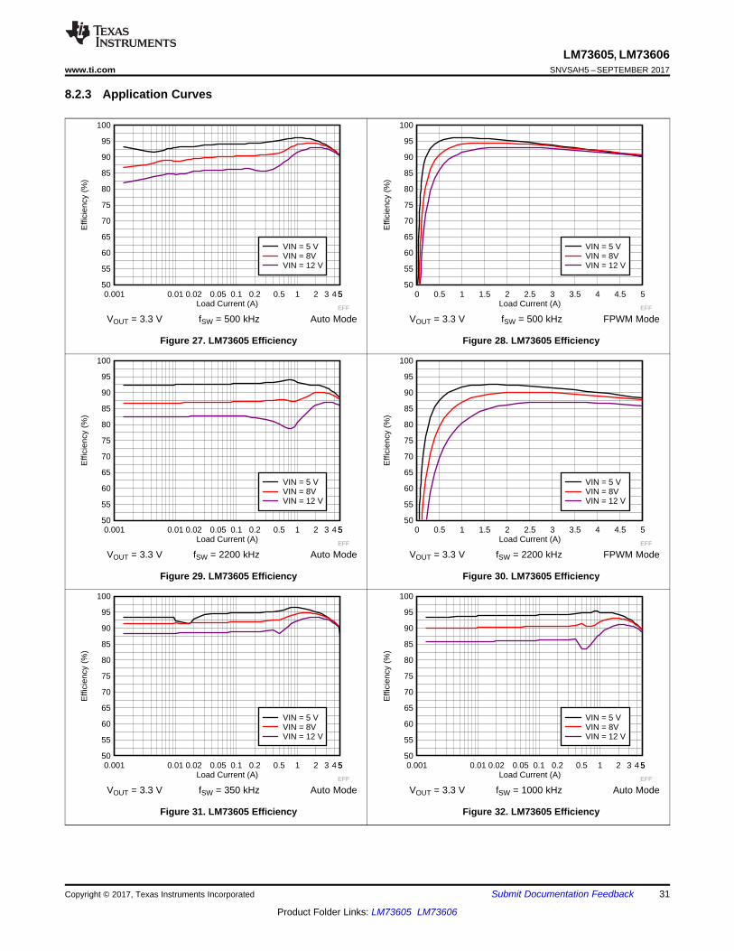
Load Current (A)
Effi
cien
cy (
%)
0.001 0.01 0.02 0.05 0.1 0.2 0.5 1 2 3 4 5550
55
60
65
70
75
80
85
90
95
100
EFF_
VIN = 5 VVIN = 8VVIN = 12 V
Load Current (A)
Effi
cien
cy (
%)
0.001 0.01 0.02 0.05 0.1 0.2 0.5 1 2 3 4 5550
55
60
65
70
75
80
85
90
95
100
EFF_
VIN = 5 VVIN = 8VVIN = 12 V
Load Current (A)
Effi
cien
cy (
%)
0.001 0.01 0.02 0.05 0.1 0.2 0.5 1 2 3 4 5550
55
60
65
70
75
80
85
90
95
100
EFF_
VIN = 5 VVIN = 8VVIN = 12 V
Load Current (A)
Effi
cien
cy (
%)
0 0.5 1 1.5 2 2.5 3 3.5 4 4.5 550
55
60
65
70
75
80
85
90
95
100
EFF_
VIN = 5 VVIN = 8VVIN = 12 V
Load Current (A)
Effi
cien
cy (
%)
0.001 0.01 0.02 0.05 0.1 0.2 0.5 1 2 3 4 5550
55
60
65
70
75
80
85
90
95
100
EFF_
VIN = 5 VVIN = 8VVIN = 12 V
Load Current (A)
Effi
cien
cy (
%)
0 0.5 1 1.5 2 2.5 3 3.5 4 4.5 550
55
60
65
70
75
80
85
90
95
100
EFF_
VIN = 5 VVIN = 8VVIN = 12 V
31
LM73605, LM73606www.ti.com SNVSAH5 –SEPTEMBER 2017
Product Folder Links: LM73605 LM73606
Submit Documentation FeedbackCopyright © 2017, Texas Instruments Incorporated
8.2.3 Application Curves
VOUT = 3.3 V fSW = 500 kHz Auto Mode
Figure 27. LM73605 Efficiency
VOUT = 3.3 V fSW = 500 kHz FPWM Mode
Figure 28. LM73605 Efficiency
VOUT = 3.3 V fSW = 2200 kHz Auto Mode
Figure 29. LM73605 Efficiency
VOUT = 3.3 V fSW = 2200 kHz FPWM Mode
Figure 30. LM73605 Efficiency
VOUT = 3.3 V fSW = 350 kHz Auto Mode
Figure 31. LM73605 Efficiency
VOUT = 3.3 V fSW = 1000 kHz Auto Mode
Figure 32. LM73605 Efficiency
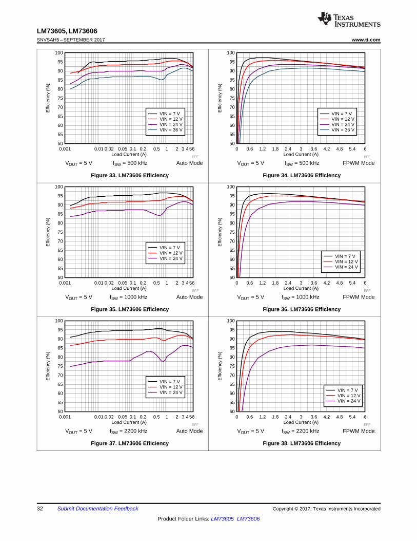
Load Current (A)
Effi
cien
cy (
%)
0.001 0.01 0.02 0.05 0.1 0.2 0.5 1 2 3 4 5650
55
60
65
70
75
80
85
90
95
100
EFF_
VIN = 7 VVIN = 12 VVIN = 24 V
Load Current (A)
Effi
cien
cy (
%)
0 0.6 1.2 1.8 2.4 3 3.6 4.2 4.8 5.4 650
55
60
65
70
75
80
85
90
95
100
EFF_
VIN = 7 VVIN = 12 VVIN = 24 V
Load Current (A)
Effi
cien
cy (
%)
0.001 0.01 0.02 0.05 0.1 0.2 0.5 1 2 3 4 5650
55
60
65
70
75
80
85
90
95
100
EFF_
VIN = 7 VVIN = 12 VVIN = 24 V
Load Current (A)
Effi
cien
cy (
%)
0 0.6 1.2 1.8 2.4 3 3.6 4.2 4.8 5.4 650
55
60
65
70
75
80
85
90
95
100
EFF_
VIN = 7 VVIN = 12 VVIN = 24 V
Load Current (A)
Effi
cien
cy (
%)
0.001 0.01 0.02 0.05 0.1 0.2 0.5 1 2 3 4 5650
55
60
65
70
75
80
85
90
95
100
EFF_
VIN = 7 VVIN = 12 VVIN = 24 VVIN = 36 V
Load Current (A)
Effi
cien
cy (
%)
0 0.6 1.2 1.8 2.4 3 3.6 4.2 4.8 5.4 650
55
60
65
70
75
80
85
90
95
100
EFF_
VIN = 7 VVIN = 12 VVIN = 24 VVIN = 36 V
32
LM73605, LM73606SNVSAH5 –SEPTEMBER 2017 www.ti.com
Product Folder Links: LM73605 LM73606
Submit Documentation Feedback Copyright © 2017, Texas Instruments Incorporated
VOUT = 5 V fSW = 500 kHz Auto Mode
Figure 33. LM73606 Efficiency
VOUT = 5 V fSW = 500 kHz FPWM Mode
Figure 34. LM73606 Efficiency
VOUT = 5 V fSW = 1000 kHz Auto Mode
Figure 35. LM73606 Efficiency
VOUT = 5 V fSW = 1000 kHz FPWM Mode
Figure 36. LM73606 Efficiency
VOUT = 5 V fSW = 2200 kHz Auto Mode
Figure 37. LM73606 Efficiency
VOUT = 5 V fSW = 2200 kHz FPWM Mode
Figure 38. LM73606 Efficiency
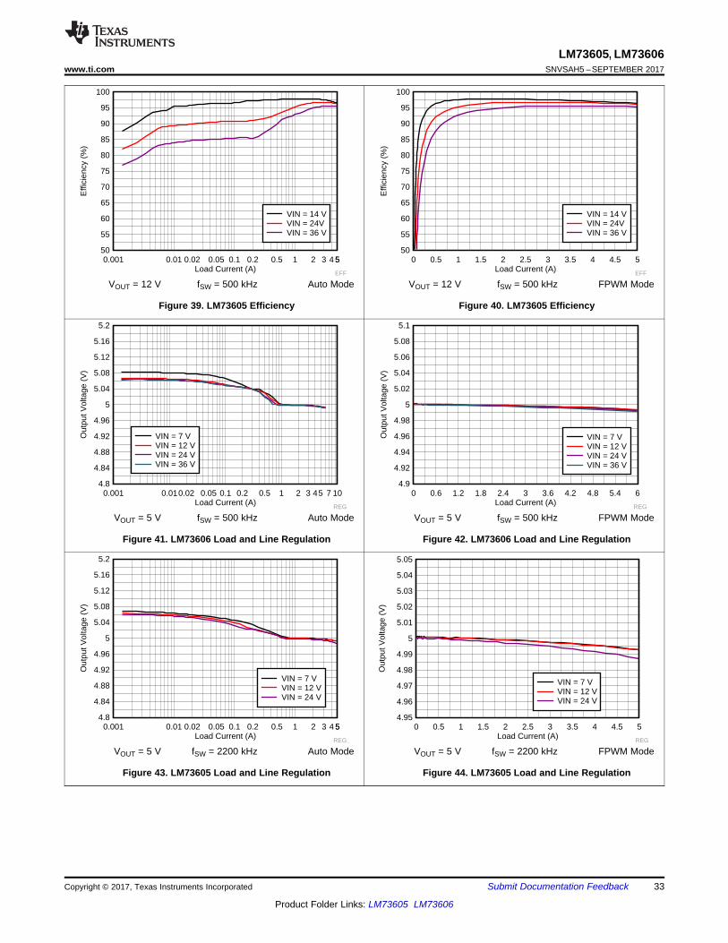
Load Current (A)
Out
put V
olta
ge (
V)
0.001 0.01 0.02 0.05 0.1 0.2 0.5 1 2 3 4 554.8
4.84
4.88
4.92
4.96
5
5.04
5.08
5.12
5.16
5.2
REG_
VIN = 7 VVIN = 12 VVIN = 24 V
Load Current (A)
Out
put V
olta
ge (
V)
0 0.5 1 1.5 2 2.5 3 3.5 4 4.5 54.95
4.96
4.97
4.98
4.99
5
5.01
5.02
5.03
5.04
5.05
REG_
VIN = 7 VVIN = 12 VVIN = 24 V
Load Current (A)
Out
put V
olta
ge (
V)
0.001 0.010.02 0.05 0.1 0.2 0.5 1 2 3 45 7 104.8
4.84
4.88
4.92
4.96
5
5.04
5.08
5.12
5.16
5.2
REG_
VIN = 7 VVIN = 12 VVIN = 24 VVIN = 36 V
Load Current (A)
Out
put V
olta
ge (
V)
0 0.6 1.2 1.8 2.4 3 3.6 4.2 4.8 5.4 64.9
4.92
4.94
4.96
4.98
5
5.02
5.04
5.06
5.08
5.1
REG_
VIN = 7 VVIN = 12 VVIN = 24 VVIN = 36 V
Load Current (A)
Effi
cien
cy (
%)
0.001 0.01 0.02 0.05 0.1 0.2 0.5 1 2 3 4 5550
55
60
65
70
75
80
85
90
95
100
EFF_
VIN = 14 VVIN = 24VVIN = 36 V
Load Current (A)
Effi
cien
cy (
%)
0 0.5 1 1.5 2 2.5 3 3.5 4 4.5 550
55
60
65
70
75
80
85
90
95
100
EFF_
VIN = 14 VVIN = 24VVIN = 36 V
33
LM73605, LM73606www.ti.com SNVSAH5 –SEPTEMBER 2017
Product Folder Links: LM73605 LM73606
Submit Documentation FeedbackCopyright © 2017, Texas Instruments Incorporated
VOUT = 12 V fSW = 500 kHz Auto Mode
Figure 39. LM73605 Efficiency
VOUT = 12 V fSW = 500 kHz FPWM Mode
Figure 40. LM73605 Efficiency
VOUT = 5 V fSW = 500 kHz Auto Mode
Figure 41. LM73606 Load and Line Regulation
VOUT = 5 V fSW = 500 kHz FPWM Mode
Figure 42. LM73606 Load and Line Regulation
VOUT = 5 V fSW = 2200 kHz Auto Mode
Figure 43. LM73605 Load and Line Regulation
VOUT = 5 V fSW = 2200 kHz FPWM Mode
Figure 44. LM73605 Load and Line Regulation
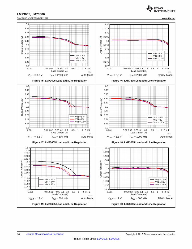
Load Current (A)
Out
put V
olta
ge (
V)
0.001 0.01 0.02 0.05 0.1 0.2 0.5 1 2 3 4 5511.8
11.8411.8811.9211.96
1212.0412.0812.1212.16
12.212.2412.2812.3212.36
12.4
REG_
VIN = 14 VVIN = 24VVIN = 36 V
Load Current (A)
Out
put V
olta
ge (
V)
0.001 0.01 0.02 0.05 0.1 0.2 0.5 1 2 3 4 5511.9
11.92
11.94
11.96
11.98
12
12.02
12.04
12.06
12.08
12.1
REG_
VIN = 14 VVIN = 24VVIN = 36 V
Load Current (A)
Out
put V
olta
ge (
V)
0.001 0.01 0.02 0.05 0.1 0.2 0.5 1 2 3 4 553.2
3.22
3.24
3.26
3.28
3.3
3.32
3.34
3.36
3.38
3.4
REG_
VIN = 5 VVIN = 8VVIN = 12 V
Load Current (A)
Out
put V
olta
ge (
V)
0.001 0.01 0.02 0.05 0.1 0.2 0.5 1 2 3 4 553.2
3.22
3.24
3.26
3.28
3.3
3.32
3.34
3.36
3.38
3.4
REG_
VIN = 5 VVIN = 8VVIN = 12 V
Load Current (A)
Out
put V
olta
ge (
V)
0.001 0.01 0.02 0.05 0.1 0.2 0.5 1 2 3 4 553.2
3.22
3.24
3.26
3.28
3.3
3.32
3.34
3.36
3.38
3.4
REG_
VIN = 5 VVIN = 8VVIN = 12 V
Load Current (A)
Out
put V
olta
ge (
V)
0.001 0.01 0.02 0.05 0.1 0.2 0.5 1 2 3 4 553.27
3.275
3.28
3.285
3.29
3.295
3.3
3.305
3.31
3.315
3.32
REG_
VIN = 5 VVIN = 8VVIN = 12 V
34
LM73605, LM73606SNVSAH5 –SEPTEMBER 2017 www.ti.com
Product Folder Links: LM73605 LM73606
Submit Documentation Feedback Copyright © 2017, Texas Instruments Incorporated
VOUT = 3.3 V fSW = 2200 kHz Auto Mode
Figure 45. LM73605 Load and Line Regulation
VOUT = 3.3 V fSW = 2200 kHz FPWM Mode
Figure 46. LM73605 Load and Line Regulation
VOUT = 3.3 V fSW = 500 kHz Auto Mode
Figure 47. LM73605 Load and Line Regulation
VOUT = 3.3 V fSW = 1000 kHz Auto Mode
Figure 48. LM73605 Load and Line Regulation
VOUT = 12 V fSW = 500 kHz Auto Mode
Figure 49. LM73605 Load and Line Regulation
VOUT = 12 V fSW = 500 kHz FPWM Mode
Figure 50. LM73605 Load and Line Regulation
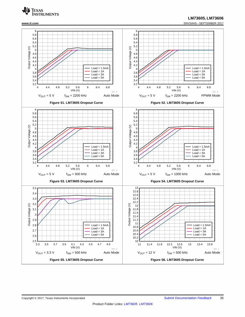
VIN (V)
Out
put V
olta
ge (
V)
3.3 3.5 3.7 3.9 4.1 4.3 4.5 4.7 4.92.5
2.6
2.7
2.8
2.9
3
3.1
3.2
3.3
3.4
3.5
DO_3
Load = 1.5mALoad = 1ALoad = 3ALoad = 5A
VIN (V)
Out
put V
olta
ge (
V)
11 11.4 11.8 12.2 12.6 13 13.4 13.810
10.210.410.610.8
1111.211.411.611.8
1212.212.412.612.8
13
DO_1
Load = 1.5mALoad = 1ALoad = 3ALoad = 5A
VIN (V)
Out
put V
olta
ge (
V)
4 4.4 4.8 5.2 5.6 6 6.4 6.83.23.43.63.8
44.24.44.64.8
55.25.45.65.8
6
DO_5
Load = 1.5mALoad = 1ALoad = 3ALoad = 5A
VIN (V)
Out
put V
olta
ge (
V)
4 4.4 4.8 5.2 5.6 6 6.4 6.83.23.43.63.8
44.24.44.64.8
55.25.45.65.8
6
DO_5
Load = 1.5mALoad = 1ALoad = 3ALoad = 5A
VIN (V)
Out
put V
olta
ge (
V)
4 4.4 4.8 5.2 5.6 6 6.4 6.83.23.43.63.8
44.24.44.64.8
55.25.45.65.8
6
DO_5
Load = 1.5mALoad = 1ALoad = 3ALoad = 5A
VIN (V)
Out
put V
olta
ge (
V)
4 4.4 4.8 5.2 5.6 6 6.4 6.83.23.43.63.8
44.24.44.64.8
55.25.45.65.8
6
DO_5
Load = 1.5mALoad = 1ALoad = 3ALoad = 5A
35
LM73605, LM73606www.ti.com SNVSAH5 –SEPTEMBER 2017
Product Folder Links: LM73605 LM73606
Submit Documentation FeedbackCopyright © 2017, Texas Instruments Incorporated
VOUT = 5 V fSW = 2200 kHz Auto Mode
Figure 51. LM73605 Dropout Curve
VOUT = 5 V fSW = 2200 kHz FPWM Mode
Figure 52. LM73605 Dropout Curve
VOUT = 5 V fSW = 500 kHz Auto Mode
Figure 53. LM73605 Dropout Curve
VOUT = 5 V fSW = 1000 kHz Auto Mode
Figure 54. LM73605 Dropout Curve
VOUT = 3.3 V fSW = 500 kHz Auto Mode
Figure 55. LM73605 Dropout Curve
VOUT = 12 V fSW = 500 kHz Auto Mode
Figure 56. LM73605 Dropout Curve
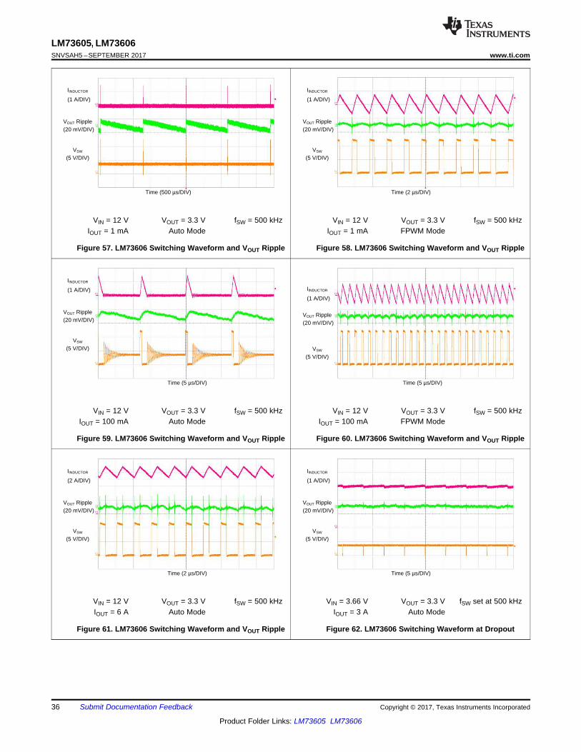
VOUT Ripple
VSW
(2 A/DIV)
Time (2 µs/DIV)
IINDUCTOR
(20 mV/DIV)
(5 V/DIV)
VOUT Ripple
VSW
(1 A/DIV)
Time (5 µs/DIV)
IINDUCTOR
(20 mV/DIV)
(5 V/DIV)
VOUT Ripple
VSW
(1 A/DIV)
Time (5 µs/DIV)
IINDUCTOR
(20 mV/DIV)
(5 V/DIV)
VOUT Ripple
VSW
(1 A/DIV)
Time (5 µs/DIV)
IINDUCTOR
(20 mV/DIV)
(5 V/DIV)
VOUT Ripple
VSW
(1 A/DIV)
Time (500 µs/DIV)
IINDUCTOR
(20 mV/DIV)
(5 V/DIV)
VOUT Ripple
VSW
(1 A/DIV)
Time (2 µs/DIV)
IINDUCTOR
(20 mV/DIV)
(5 V/DIV)
36
LM73605, LM73606SNVSAH5 –SEPTEMBER 2017 www.ti.com
Product Folder Links: LM73605 LM73606
Submit Documentation Feedback Copyright © 2017, Texas Instruments Incorporated
VIN = 12 V VOUT = 3.3 V fSW = 500 kHzIOUT = 1 mA Auto Mode
Figure 57. LM73606 Switching Waveform and VOUT Ripple
VIN = 12 V VOUT = 3.3 V fSW = 500 kHzIOUT = 1 mA FPWM Mode
Figure 58. LM73606 Switching Waveform and VOUT Ripple
VIN = 12 V VOUT = 3.3 V fSW = 500 kHzIOUT = 100 mA Auto Mode
Figure 59. LM73606 Switching Waveform and VOUT Ripple
VIN = 12 V VOUT = 3.3 V fSW = 500 kHzIOUT = 100 mA FPWM Mode
Figure 60. LM73606 Switching Waveform and VOUT Ripple
VIN = 12 V VOUT = 3.3 V fSW = 500 kHzIOUT = 6 A Auto Mode
Figure 61. LM73606 Switching Waveform and VOUT Ripple
VIN = 3.66 V VOUT = 3.3 V fSW set at 500 kHzIOUT = 3 A Auto Mode
Figure 62. LM73606 Switching Waveform at Dropout
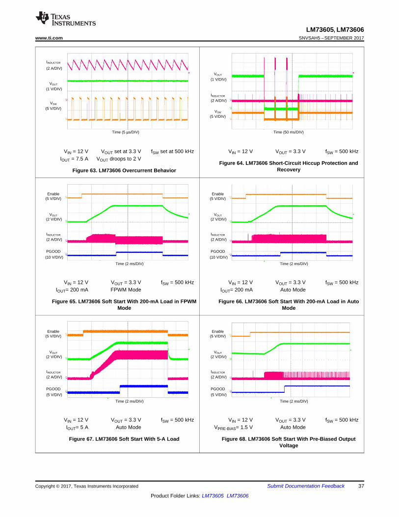
VOUT
Enable
(2 A/DIV)
Time (2 ms/DIV)
IINDUCTOR
(2 V/DIV)
(5 V/DIV)
(5 V/DIV)
PGOOD
VOUT
Enable
(2 A/DIV)
Time (2 ms/DIV)
IINDUCTOR
(2 V/DIV)
(5 V/DIV)
(5 V/DIV)
PGOOD
VOUT
Enable
(2 A/DIV)
Time (2 ms/DIV)
IINDUCTOR
(2 V/DIV)
(5 V/DIV)
(10 V/DIV)
PGOOD
VOUT
Enable
(2 A/DIV)
Time (2 ms/DIV)
IINDUCTOR
(2 V/DIV)
(5 V/DIV)
(10 V/DIV)
PGOOD
VOUT
VSW
(2 A/DIV)
Time (5 µs/DIV)
IINDUCTOR
(1 V/DIV)
(5 V/DIV)
VOUT
VSW
(2 A/DIV)
Time (50 ms/DIV)
IINDUCTOR
(1 V/DIV)
(5 V/DIV)
37
LM73605, LM73606www.ti.com SNVSAH5 –SEPTEMBER 2017
Product Folder Links: LM73605 LM73606
Submit Documentation FeedbackCopyright © 2017, Texas Instruments Incorporated
VIN = 12 V VOUT set at 3.3 V fSW set at 500 kHzIOUT = 7.5 A VOUT droops to 2 V
Figure 63. LM73606 Overcurrent Behavior
VIN = 12 V VOUT = 3.3 V fSW = 500 kHz
Figure 64. LM73606 Short-Circuit Hiccup Protection andRecovery
VIN = 12 V VOUT = 3.3 V fSW = 500 kHzIOUT= 200 mA FPWM Mode
Figure 65. LM73606 Soft Start With 200-mA Load in FPWMMode
VIN = 12 V VOUT = 3.3 V fSW = 500 kHzIOUT= 200 mA Auto Mode
Figure 66. LM73606 Soft Start With 200-mA Load in AutoMode
VIN = 12 V VOUT = 3.3 V fSW = 500 kHzIOUT= 5 A Auto Mode
Figure 67. LM73606 Soft Start With 5-A Load
VIN = 12 V VOUT = 3.3 V fSW = 500 kHzVPRE-BIAS= 1.5 V Auto Mode
Figure 68. LM73606 Soft Start With Pre-Biased OutputVoltage
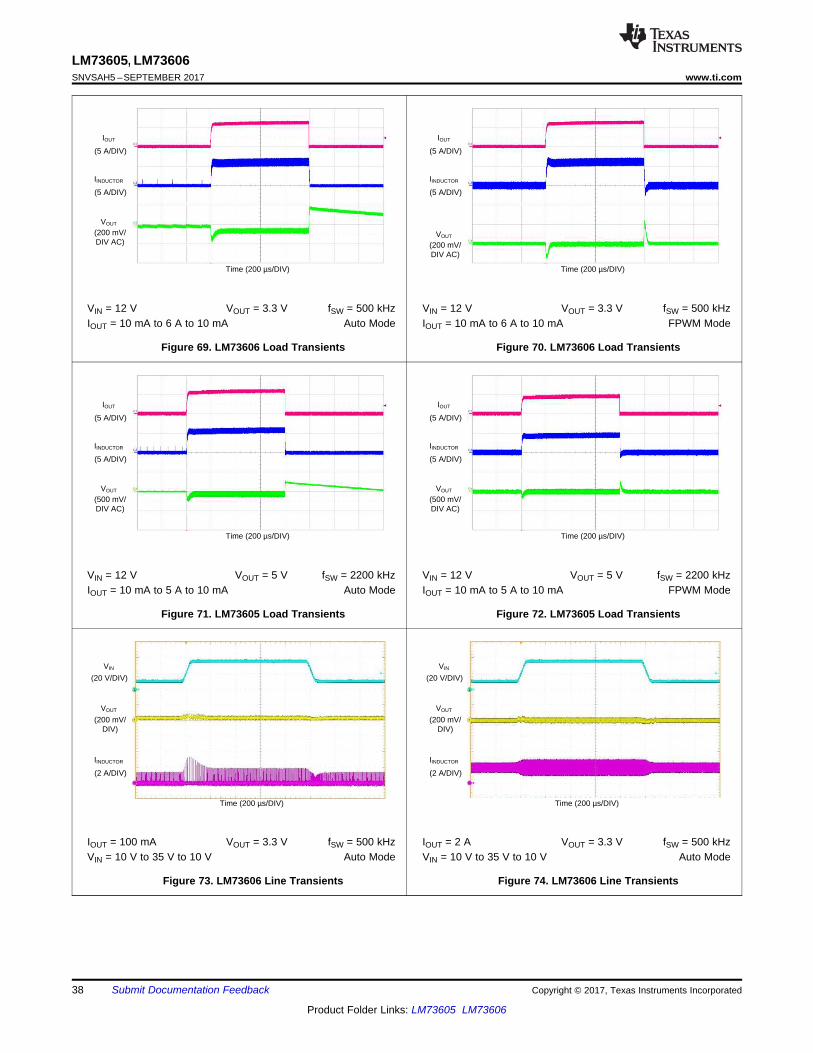
VOUT
VIN
(2 A/DIV)
Time (200 µs/DIV)
IINDUCTOR
(200 mV/DIV)
(20 V/DIV)
VOUT
VIN
(2 A/DIV)
Time (200 µs/DIV)
IINDUCTOR
(200 mV/DIV)
(20 V/DIV)
VOUT
(5 A/DIV)
Time (200 µs/DIV)
IINDUCTOR
(500 mV/DIV AC)
(5 A/DIV)
IOUT
VOUT
(5 A/DIV)
Time (200 µs/DIV)
IINDUCTOR
(500 mV/DIV AC)
(5 A/DIV)
IOUT
VOUT
(5 A/DIV)
Time (200 µs/DIV)
IINDUCTOR
(200 mV/DIV AC)
(5 A/DIV)
IOUT
VOUT
(5 A/DIV)
Time (200 µs/DIV)
IINDUCTOR
(200 mV/DIV AC)
(5 A/DIV)
IOUT
38
LM73605, LM73606SNVSAH5 –SEPTEMBER 2017 www.ti.com
Product Folder Links: LM73605 LM73606
Submit Documentation Feedback Copyright © 2017, Texas Instruments Incorporated
VIN = 12 V VOUT = 3.3 V fSW = 500 kHzIOUT = 10 mA to 6 A to 10 mA Auto Mode
Figure 69. LM73606 Load Transients
VIN = 12 V VOUT = 3.3 V fSW = 500 kHzIOUT = 10 mA to 6 A to 10 mA FPWM Mode
Figure 70. LM73606 Load Transients
VIN = 12 V VOUT = 5 V fSW = 2200 kHzIOUT = 10 mA to 5 A to 10 mA Auto Mode
Figure 71. LM73605 Load Transients
VIN = 12 V VOUT = 5 V fSW = 2200 kHzIOUT = 10 mA to 5 A to 10 mA FPWM Mode
Figure 72. LM73605 Load Transients
IOUT = 100 mA VOUT = 3.3 V fSW = 500 kHzVIN = 10 V to 35 V to 10 V Auto Mode
Figure 73. LM73606 Line Transients
IOUT = 2 A VOUT = 3.3 V fSW = 500 kHzVIN = 10 V to 35 V to 10 V Auto Mode
Figure 74. LM73606 Line Transients
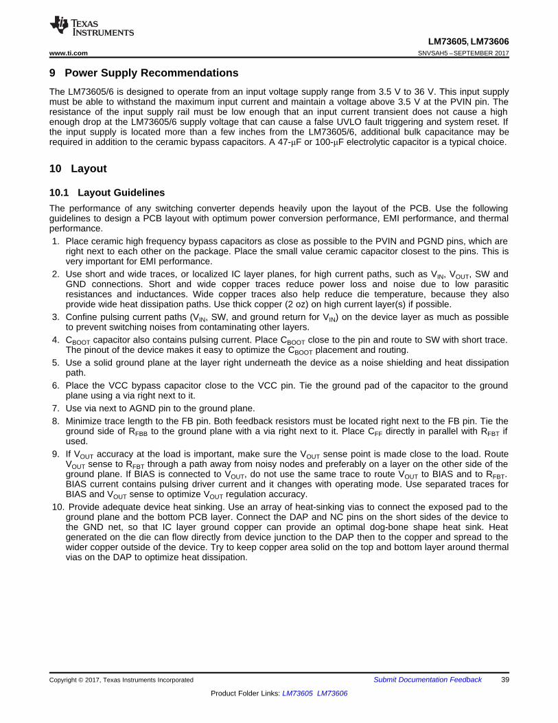
39
LM73605, LM73606www.ti.com SNVSAH5 –SEPTEMBER 2017
Product Folder Links: LM73605 LM73606
Submit Documentation FeedbackCopyright © 2017, Texas Instruments Incorporated
9 Power Supply RecommendationsThe LM73605/6 is designed to operate from an input voltage supply range from 3.5 V to 36 V. This input supplymust be able to withstand the maximum input current and maintain a voltage above 3.5 V at the PVIN pin. Theresistance of the input supply rail must be low enough that an input current transient does not cause a highenough drop at the LM73605/6 supply voltage that can cause a false UVLO fault triggering and system reset. Ifthe input supply is located more than a few inches from the LM73605/6, additional bulk capacitance may berequired in addition to the ceramic bypass capacitors. A 47-μF or 100-μF electrolytic capacitor is a typical choice.
10 Layout
10.1 Layout GuidelinesThe performance of any switching converter depends heavily upon the layout of the PCB. Use the followingguidelines to design a PCB layout with optimum power conversion performance, EMI performance, and thermalperformance.1. Place ceramic high frequency bypass capacitors as close as possible to the PVIN and PGND pins, which are
right next to each other on the package. Place the small value ceramic capacitor closest to the pins. This isvery important for EMI performance.
2. Use short and wide traces, or localized IC layer planes, for high current paths, such as VIN, VOUT, SW andGND connections. Short and wide copper traces reduce power loss and noise due to low parasiticresistances and inductances. Wide copper traces also help reduce die temperature, because they alsoprovide wide heat dissipation paths. Use thick copper (2 oz) on high current layer(s) if possible.
3. Confine pulsing current paths (VIN, SW, and ground return for VIN) on the device layer as much as possibleto prevent switching noises from contaminating other layers.
4. CBOOT capacitor also contains pulsing current. Place CBOOT close to the pin and route to SW with short trace.The pinout of the device makes it easy to optimize the CBOOT placement and routing.
5. Use a solid ground plane at the layer right underneath the device as a noise shielding and heat dissipationpath.
6. Place the VCC bypass capacitor close to the VCC pin. Tie the ground pad of the capacitor to the groundplane using a via right next to it.
7. Use via next to AGND pin to the ground plane.8. Minimize trace length to the FB pin. Both feedback resistors must be located right next to the FB pin. Tie the
ground side of RFBB to the ground plane with a via right next to it. Place CFF directly in parallel with RFBT ifused.
9. If VOUT accuracy at the load is important, make sure the VOUT sense point is made close to the load. RouteVOUT sense to RFBT through a path away from noisy nodes and preferably on a layer on the other side of theground plane. If BIAS is connected to VOUT, do not use the same trace to route VOUT to BIAS and to RFBT.BIAS current contains pulsing driver current and it changes with operating mode. Use separated traces forBIAS and VOUT sense to optimize VOUT regulation accuracy.
10. Provide adequate device heat sinking. Use an array of heat-sinking vias to connect the exposed pad to theground plane and the bottom PCB layer. Connect the DAP and NC pins on the short sides of the device tothe GND net, so that IC layer ground copper can provide an optimal dog-bone shape heat sink. Heatgenerated on the die can flow directly from device junction to the DAP then to the copper and spread to thewider copper outside of the device. Try to keep copper area solid on the top and bottom layer around thermalvias on the DAP to optimize heat dissipation.
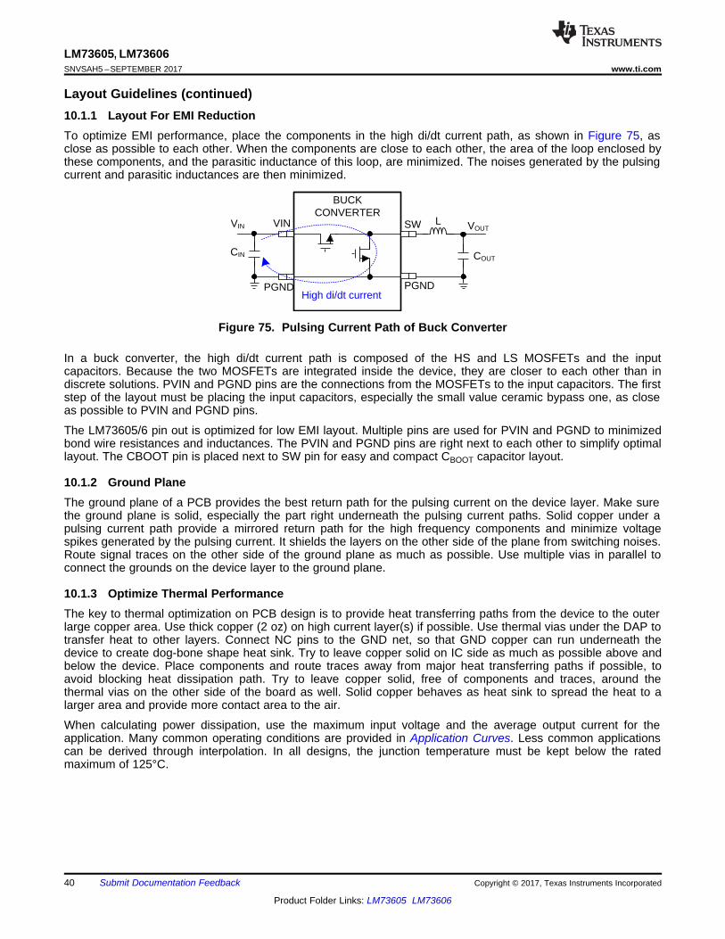
SWVIN
PGNDPGND
CIN
VIN
COUT
VOUTL
High di/dt current
BUCK CONVERTER
40
LM73605, LM73606SNVSAH5 –SEPTEMBER 2017 www.ti.com
Product Folder Links: LM73605 LM73606
Submit Documentation Feedback Copyright © 2017, Texas Instruments Incorporated
Layout Guidelines (continued)10.1.1 Layout For EMI ReductionTo optimize EMI performance, place the components in the high di/dt current path, as shown in Figure 75, asclose as possible to each other. When the components are close to each other, the area of the loop enclosed bythese components, and the parasitic inductance of this loop, are minimized. The noises generated by the pulsingcurrent and parasitic inductances are then minimized.
Figure 75. Pulsing Current Path of Buck Converter
In a buck converter, the high di/dt current path is composed of the HS and LS MOSFETs and the inputcapacitors. Because the two MOSFETs are integrated inside the device, they are closer to each other than indiscrete solutions. PVIN and PGND pins are the connections from the MOSFETs to the input capacitors. The firststep of the layout must be placing the input capacitors, especially the small value ceramic bypass one, as closeas possible to PVIN and PGND pins.
The LM73605/6 pin out is optimized for low EMI layout. Multiple pins are used for PVIN and PGND to minimizedbond wire resistances and inductances. The PVIN and PGND pins are right next to each other to simplify optimallayout. The CBOOT pin is placed next to SW pin for easy and compact CBOOT capacitor layout.
10.1.2 Ground PlaneThe ground plane of a PCB provides the best return path for the pulsing current on the device layer. Make surethe ground plane is solid, especially the part right underneath the pulsing current paths. Solid copper under apulsing current path provide a mirrored return path for the high frequency components and minimize voltagespikes generated by the pulsing current. It shields the layers on the other side of the plane from switching noises.Route signal traces on the other side of the ground plane as much as possible. Use multiple vias in parallel toconnect the grounds on the device layer to the ground plane.
10.1.3 Optimize Thermal PerformanceThe key to thermal optimization on PCB design is to provide heat transferring paths from the device to the outerlarge copper area. Use thick copper (2 oz) on high current layer(s) if possible. Use thermal vias under the DAP totransfer heat to other layers. Connect NC pins to the GND net, so that GND copper can run underneath thedevice to create dog-bone shape heat sink. Try to leave copper solid on IC side as much as possible above andbelow the device. Place components and route traces away from major heat transferring paths if possible, toavoid blocking heat dissipation path. Try to leave copper solid, free of components and traces, around thethermal vias on the other side of the board as well. Solid copper behaves as heat sink to spread the heat to alarger area and provide more contact area to the air.
When calculating power dissipation, use the maximum input voltage and the average output current for theapplication. Many common operating conditions are provided in Application Curves. Less common applicationscan be derived through interpolation. In all designs, the junction temperature must be kept below the ratedmaximum of 125°C.
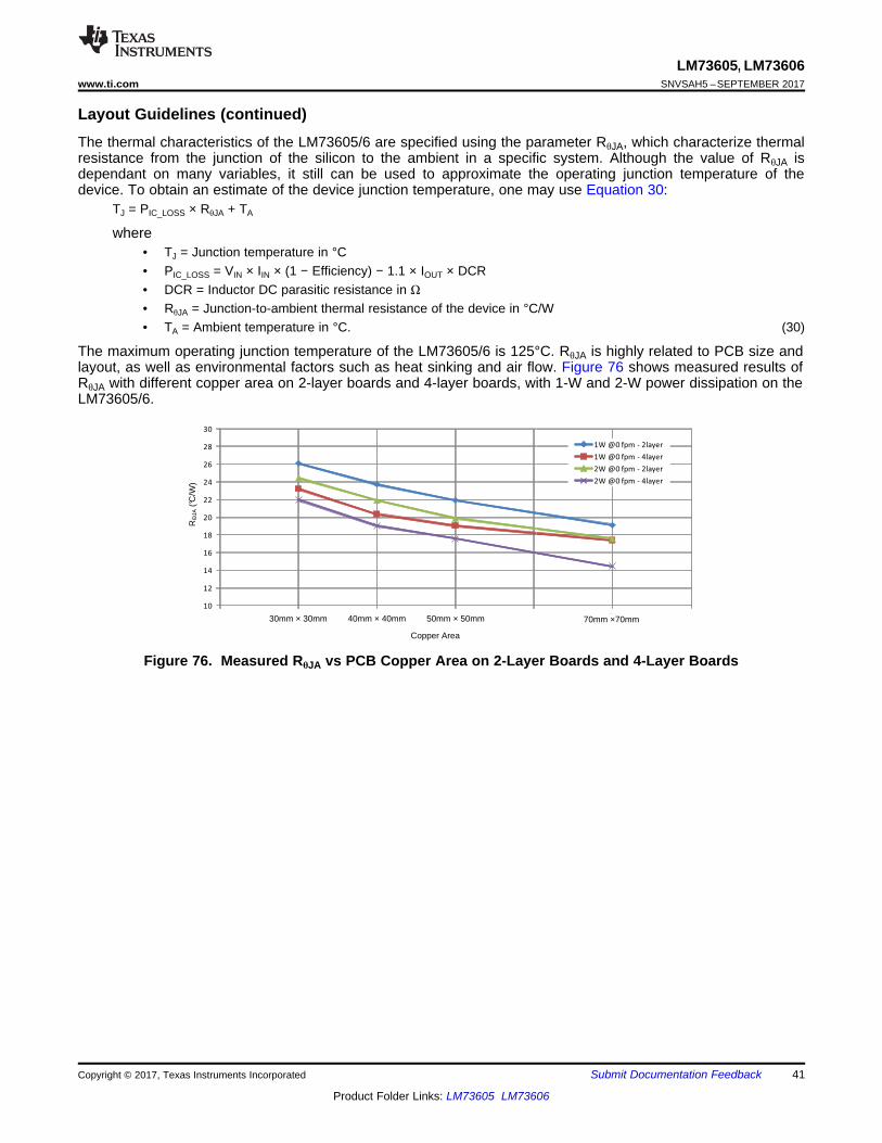
10
12
14
16
18
20
22
24
26
28
30
20 30 40 50 60 70 80
1W @0 fpm - 2layer
1W @0 fpm - 4layer
2W @0 fpm - 2layer
2W @0 fpm - 4layer
Copper Area
R,
JA (
°C/W
)
30mm × 30mm 40mm × 40mm 50mm × 50mm 70mm ×70mm
41
LM73605, LM73606www.ti.com SNVSAH5 –SEPTEMBER 2017
Product Folder Links: LM73605 LM73606
Submit Documentation FeedbackCopyright © 2017, Texas Instruments Incorporated
Layout Guidelines (continued)The thermal characteristics of the LM73605/6 are specified using the parameter RθJA, which characterize thermalresistance from the junction of the silicon to the ambient in a specific system. Although the value of RθJA isdependant on many variables, it still can be used to approximate the operating junction temperature of thedevice. To obtain an estimate of the device junction temperature, one may use Equation 30:
TJ = PIC_LOSS × RθJA + TA
where• TJ = Junction temperature in °C• PIC_LOSS = VIN × IIN × (1 − Efficiency) − 1.1 × IOUT × DCR• DCR = Inductor DC parasitic resistance in Ω• RθJA = Junction-to-ambient thermal resistance of the device in °C/W• TA = Ambient temperature in °C. (30)
The maximum operating junction temperature of the LM73605/6 is 125°C. RθJA is highly related to PCB size andlayout, as well as environmental factors such as heat sinking and air flow. Figure 76 shows measured results ofRθJA with different copper area on 2-layer boards and 4-layer boards, with 1-W and 2-W power dissipation on theLM73605/6.
Figure 76. Measured RθJA vs PCB Copper Area on 2-Layer Boards and 4-Layer Boards
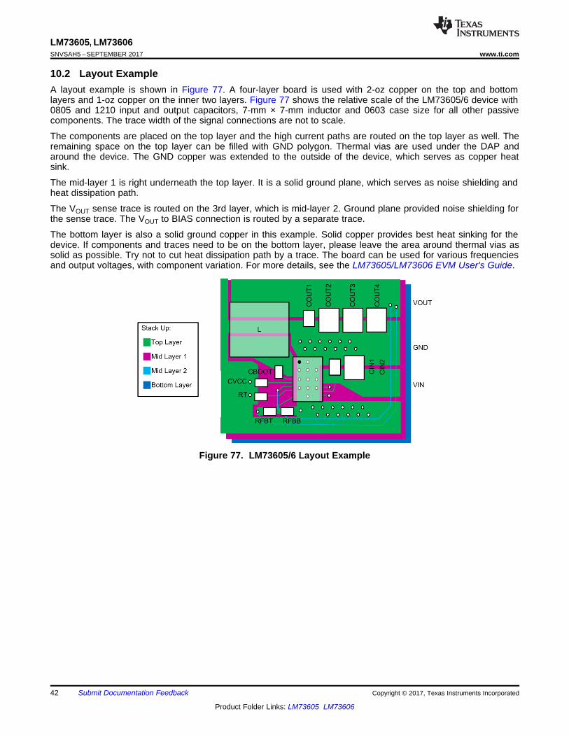
42
LM73605, LM73606SNVSAH5 –SEPTEMBER 2017 www.ti.com
Product Folder Links: LM73605 LM73606
Submit Documentation Feedback Copyright © 2017, Texas Instruments Incorporated
10.2 Layout ExampleA layout example is shown in Figure 77. A four-layer board is used with 2-oz copper on the top and bottomlayers and 1-oz copper on the inner two layers. Figure 77 shows the relative scale of the LM73605/6 device with0805 and 1210 input and output capacitors, 7-mm × 7-mm inductor and 0603 case size for all other passivecomponents. The trace width of the signal connections are not to scale.
The components are placed on the top layer and the high current paths are routed on the top layer as well. Theremaining space on the top layer can be filled with GND polygon. Thermal vias are used under the DAP andaround the device. The GND copper was extended to the outside of the device, which serves as copper heatsink.
The mid-layer 1 is right underneath the top layer. It is a solid ground plane, which serves as noise shielding andheat dissipation path.
The VOUT sense trace is routed on the 3rd layer, which is mid-layer 2. Ground plane provided noise shielding forthe sense trace. The VOUT to BIAS connection is routed by a separate trace.
The bottom layer is also a solid ground copper in this example. Solid copper provides best heat sinking for thedevice. If components and traces need to be on the bottom layer, please leave the area around thermal vias assolid as possible. Try not to cut heat dissipation path by a trace. The board can be used for various frequenciesand output voltages, with component variation. For more details, see the LM73605/LM73606 EVM User's Guide.
Figure 77. LM73605/6 Layout Example
43
LM73605, LM73606www.ti.com SNVSAH5 –SEPTEMBER 2017
Product Folder Links: LM73605 LM73606
Submit Documentation FeedbackCopyright © 2017, Texas Instruments Incorporated
11 Device and Documentation Support
11.1 Device Support
11.1.1 Third-Party Products DisclaimerTI'S PUBLICATION OF INFORMATION REGARDING THIRD-PARTY PRODUCTS OR SERVICES DOES NOTCONSTITUTE AN ENDORSEMENT REGARDING THE SUITABILITY OF SUCH PRODUCTS OR SERVICESOR A WARRANTY, REPRESENTATION OR ENDORSEMENT OF SUCH PRODUCTS OR SERVICES, EITHERALONE OR IN COMBINATION WITH ANY TI PRODUCT OR SERVICE.
11.1.2 Custom Design With WEBENCH® ToolsClick here to create a custom design using the LM73605 or LM73606 device with the WEBENCH® PowerDesigner.1. Start by entering the input voltage (VIN), output voltage (VOUT), and output current (IOUT) requirements.2. Optimize the design for key parameters such as efficiency, footprint, and cost using the optimizer dial.3. Compare the generated design with other possible solutions from Texas Instruments.
The WEBENCH Power Designer provides a customized schematic along with a list of materials with real-timepricing and component availability.
In most cases, these actions are available:• Run electrical simulations to see important waveforms and circuit performance• Run thermal simulations to understand board thermal performance• Export customized schematic and layout into popular CAD formats• Print PDF reports for the design, and share the design with colleagues
Get more information about WEBENCH tools at www.ti.com/WEBENCH.
11.2 Related DocumentationFor related documentation see the following:
AN-2020 Thermal Design By Insight, Not Hindsight
11.3 Related LinksThe table below lists quick access links. Categories include technical documents, support and communityresources, tools and software, and quick access to order now.
Table 5. Related Links
PARTS PRODUCT FOLDER ORDER NOW TECHNICALDOCUMENTS
TOOLS &SOFTWARE
SUPPORT &COMMUNITY
LM73605 Click here Click here Click here Click here Click hereLM73606 Click here Click here Click here Click here Click here
11.4 Receiving Notification of Documentation UpdatesTo receive notification of documentation updates, navigate to the device product folder on ti.com. In the upperright corner, click on Alert me to register and receive a weekly digest of any product information that haschanged. For change details, review the revision history included in any revised document.
44
LM73605, LM73606SNVSAH5 –SEPTEMBER 2017 www.ti.com
Product Folder Links: LM73605 LM73606
Submit Documentation Feedback Copyright © 2017, Texas Instruments Incorporated
11.5 Community ResourcesThe following links connect to TI community resources. Linked contents are provided "AS IS" by the respectivecontributors. They do not constitute TI specifications and do not necessarily reflect TI's views; see TI's Terms ofUse.
TI E2E™ Online Community TI's Engineer-to-Engineer (E2E) Community. Created to foster collaborationamong engineers. At e2e.ti.com, you can ask questions, share knowledge, explore ideas and helpsolve problems with fellow engineers.
Design Support TI's Design Support Quickly find helpful E2E forums along with design support tools andcontact information for technical support.
11.6 TrademarksE2E is a trademark of Texas Instruments.WEBENCH is a registered trademark of Texas Instruments.SP-CAP is a trademark of Panasonic.POSCAP is a trademark of Sanyo Electric Co., Ltd..
11.7 Electrostatic Discharge CautionThese devices have limited built-in ESD protection. The leads should be shorted together or the device placed in conductive foamduring storage or handling to prevent electrostatic damage to the MOS gates.
11.8 GlossarySLYZ022 — TI Glossary.
This glossary lists and explains terms, acronyms, and definitions.
45
LM73605, LM73606www.ti.com SNVSAH5 –SEPTEMBER 2017
Product Folder Links: LM73605 LM73606
Submit Documentation FeedbackCopyright © 2017, Texas Instruments Incorporated
12 Mechanical, Packaging, and Orderable InformationThe following pages include mechanical, packaging, and orderable information. This information is the mostcurrent data available for the designated devices. This data is subject to change without notice and revision ofthis document. For browser-based versions of this data sheet, refer to the left-hand navigation.
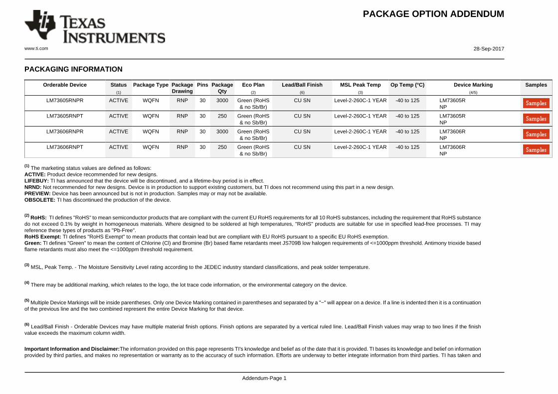
PACKAGE OPTION ADDENDUM
www.ti.com 28-Sep-2017
Addendum-Page 1
PACKAGING INFORMATION
Orderable Device Status(1)
Package Type PackageDrawing
Pins PackageQty
Eco Plan(2)
Lead/Ball Finish(6)
MSL Peak Temp(3)
Op Temp (°C) Device Marking(4/5)
Samples
LM73605RNPR ACTIVE WQFN RNP 30 3000 Green (RoHS& no Sb/Br)
CU SN Level-2-260C-1 YEAR -40 to 125 LM73605RNP
LM73605RNPT ACTIVE WQFN RNP 30 250 Green (RoHS& no Sb/Br)
CU SN Level-2-260C-1 YEAR -40 to 125 LM73605RNP
LM73606RNPR ACTIVE WQFN RNP 30 3000 Green (RoHS& no Sb/Br)
CU SN Level-2-260C-1 YEAR -40 to 125 LM73606RNP
LM73606RNPT ACTIVE WQFN RNP 30 250 Green (RoHS& no Sb/Br)
CU SN Level-2-260C-1 YEAR -40 to 125 LM73606RNP
(1) The marketing status values are defined as follows:ACTIVE: Product device recommended for new designs.LIFEBUY: TI has announced that the device will be discontinued, and a lifetime-buy period is in effect.NRND: Not recommended for new designs. Device is in production to support existing customers, but TI does not recommend using this part in a new design.PREVIEW: Device has been announced but is not in production. Samples may or may not be available.OBSOLETE: TI has discontinued the production of the device.
(2) RoHS: TI defines "RoHS" to mean semiconductor products that are compliant with the current EU RoHS requirements for all 10 RoHS substances, including the requirement that RoHS substancedo not exceed 0.1% by weight in homogeneous materials. Where designed to be soldered at high temperatures, "RoHS" products are suitable for use in specified lead-free processes. TI mayreference these types of products as "Pb-Free".RoHS Exempt: TI defines "RoHS Exempt" to mean products that contain lead but are compliant with EU RoHS pursuant to a specific EU RoHS exemption.Green: TI defines "Green" to mean the content of Chlorine (Cl) and Bromine (Br) based flame retardants meet JS709B low halogen requirements of <=1000ppm threshold. Antimony trioxide basedflame retardants must also meet the <=1000ppm threshold requirement.
(3) MSL, Peak Temp. - The Moisture Sensitivity Level rating according to the JEDEC industry standard classifications, and peak solder temperature.
(4) There may be additional marking, which relates to the logo, the lot trace code information, or the environmental category on the device.
(5) Multiple Device Markings will be inside parentheses. Only one Device Marking contained in parentheses and separated by a "~" will appear on a device. If a line is indented then it is a continuationof the previous line and the two combined represent the entire Device Marking for that device.
(6) Lead/Ball Finish - Orderable Devices may have multiple material finish options. Finish options are separated by a vertical ruled line. Lead/Ball Finish values may wrap to two lines if the finishvalue exceeds the maximum column width.
Important Information and Disclaimer:The information provided on this page represents TI's knowledge and belief as of the date that it is provided. TI bases its knowledge and belief on informationprovided by third parties, and makes no representation or warranty as to the accuracy of such information. Efforts are underway to better integrate information from third parties. TI has taken and
PACKAGE OPTION ADDENDUM
www.ti.com 28-Sep-2017
Addendum-Page 2
continues to take reasonable steps to provide representative and accurate information but may not have conducted destructive testing or chemical analysis on incoming materials and chemicals.TI and TI suppliers consider certain information to be proprietary, and thus CAS numbers and other limited information may not be available for release.
In no event shall TI's liability arising out of such information exceed the total purchase price of the TI part(s) at issue in this document sold by TI to Customer on an annual basis.
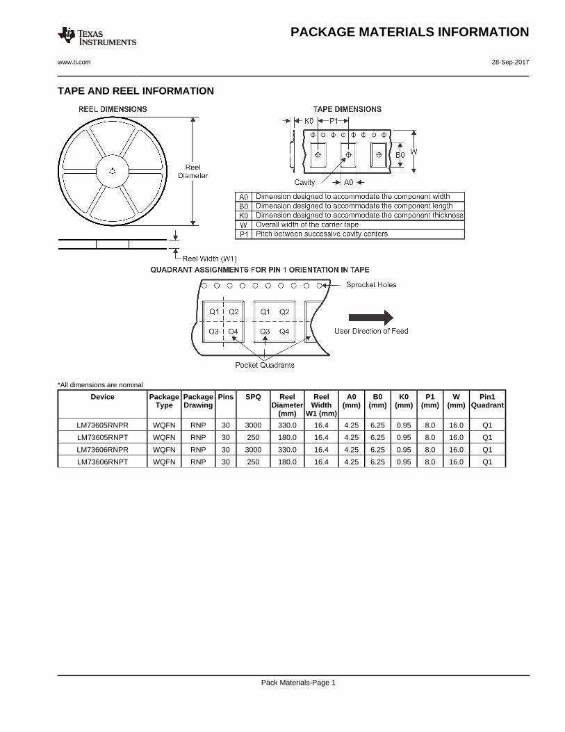
TAPE AND REEL INFORMATION
*All dimensions are nominal
Device PackageType
PackageDrawing
Pins SPQ ReelDiameter
(mm)
ReelWidth
W1 (mm)
A0(mm)
B0(mm)
K0(mm)
P1(mm)
W(mm)
Pin1Quadrant
LM73605RNPR WQFN RNP 30 3000 330.0 16.4 4.25 6.25 0.95 8.0 16.0 Q1
LM73605RNPT WQFN RNP 30 250 180.0 16.4 4.25 6.25 0.95 8.0 16.0 Q1
LM73606RNPR WQFN RNP 30 3000 330.0 16.4 4.25 6.25 0.95 8.0 16.0 Q1
LM73606RNPT WQFN RNP 30 250 180.0 16.4 4.25 6.25 0.95 8.0 16.0 Q1
PACKAGE MATERIALS INFORMATION
www.ti.com 28-Sep-2017
Pack Materials-Page 1
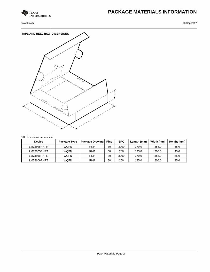
*All dimensions are nominal
Device Package Type Package Drawing Pins SPQ Length (mm) Width (mm) Height (mm)
LM73605RNPR WQFN RNP 30 3000 370.0 355.0 55.0
LM73605RNPT WQFN RNP 30 250 195.0 200.0 45.0
LM73606RNPR WQFN RNP 30 3000 370.0 355.0 55.0
LM73606RNPT WQFN RNP 30 250 195.0 200.0 45.0
PACKAGE MATERIALS INFORMATION
www.ti.com 28-Sep-2017
Pack Materials-Page 2
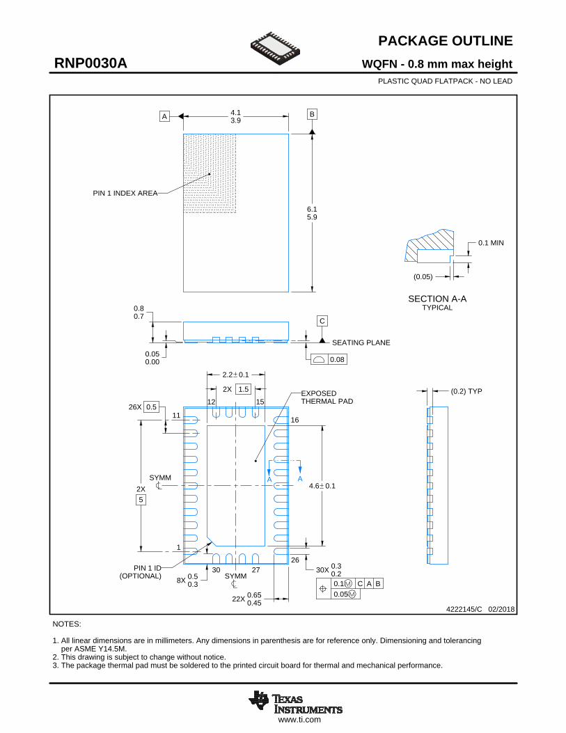
A A
www.ti.com
PACKAGE OUTLINE
C
30X 0.30.2
2.2 0.1
22X 0.650.45
0.80.7
(0.2) TYP
0.050.00
26X 0.5
2X5
4.6 0.1
2X 1.5
8X 0.50.3
A 4.13.9
B
6.15.9
0.1 MIN
(0.05)
WQFN - 0.8 mm max heightRNP0030APLASTIC QUAD FLATPACK - NO LEAD
4222145/C 02/2018
PIN 1 INDEX AREA
0.08
SEATING PLANE
1
11 16
26
12 15
30 27(OPTIONAL)
PIN 1 ID
0.1 C A B0.05
EXPOSEDTHERMAL PAD
SYMM
SYMM
NOTES: 1. All linear dimensions are in millimeters. Any dimensions in parenthesis are for reference only. Dimensioning and tolerancing per ASME Y14.5M. 2. This drawing is subject to change without notice. 3. The package thermal pad must be soldered to the printed circuit board for thermal and mechanical performance.
SCALE 2.700
SCALE 25.000SECTION A-ASECTION A-ATYPICAL
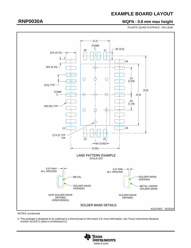
www.ti.com
EXAMPLE BOARD LAYOUT
0.07 MINALL AROUND
0.07 MAXALL AROUND
30X (0.25)
22X (0.75)
( 0.2) TYPVIA
(R0.05) TYP
2X(2.05)
(5.8)
(3.65)
(0.5) TYP
(2.2)
6X (0.85)
6X(1.16)
(4.6)
8X (0.6)
WQFN - 0.8 mm max heightRNP0030APLASTIC QUAD FLATPACK - NO LEAD
4222145/C 02/2018
SYMM
1
11
12 15
16
26
2730
SYMM
LAND PATTERN EXAMPLESCALE:15X
NOTES: (continued) 4. This package is designed to be soldered to a thermal pad on the board. For more information, see Texas Instruments literature number SLUA271 (www.ti.com/lit/slua271).
SOLDER MASKOPENING
METAL UNDERSOLDER MASK
SOLDER MASKDEFINED
METAL
SOLDER MASKOPENING
SOLDER MASK DETAILS
NON SOLDER MASKDEFINED
(PREFERRED)
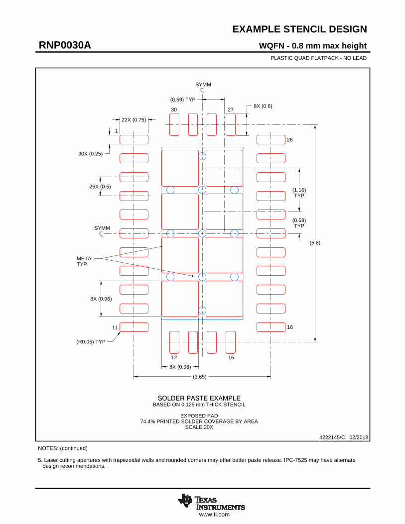
www.ti.com
EXAMPLE STENCIL DESIGN
22X (0.75)
30X (0.25)
26X (0.5)
(3.65)
(5.8)
8X (0.98)
(1.16)TYP
(0.59) TYP
(R0.05) TYP
8X (0.96)
8X (0.6)
(0.58)TYP
WQFN - 0.8 mm max heightRNP0030APLASTIC QUAD FLATPACK - NO LEAD
4222145/C 02/2018
NOTES: (continued) 5. Laser cutting apertures with trapezoidal walls and rounded corners may offer better paste release. IPC-7525 may have alternate design recommendations.
SYMM
METALTYP
SOLDER PASTE EXAMPLEBASED ON 0.125 mm THICK STENCIL
EXPOSED PAD
74.4% PRINTED SOLDER COVERAGE BY AREASCALE:20X
SYMM
1
11
12 15
16
26
2730
IMPORTANT NOTICE
Texas Instruments Incorporated (TI) reserves the right to make corrections, enhancements, improvements and other changes to itssemiconductor products and services per JESD46, latest issue, and to discontinue any product or service per JESD48, latest issue. Buyersshould obtain the latest relevant information before placing orders and should verify that such information is current and complete.TI’s published terms of sale for semiconductor products (http://www.ti.com/sc/docs/stdterms.htm) apply to the sale of packaged integratedcircuit products that TI has qualified and released to market. Additional terms may apply to the use or sale of other types of TI products andservices.Reproduction of significant portions of TI information in TI data sheets is permissible only if reproduction is without alteration and isaccompanied by all associated warranties, conditions, limitations, and notices. TI is not responsible or liable for such reproduceddocumentation. Information of third parties may be subject to additional restrictions. Resale of TI products or services with statementsdifferent from or beyond the parameters stated by TI for that product or service voids all express and any implied warranties for theassociated TI product or service and is an unfair and deceptive business practice. TI is not responsible or liable for any such statements.Buyers and others who are developing systems that incorporate TI products (collectively, “Designers”) understand and agree that Designersremain responsible for using their independent analysis, evaluation and judgment in designing their applications and that Designers havefull and exclusive responsibility to assure the safety of Designers' applications and compliance of their applications (and of all TI productsused in or for Designers’ applications) with all applicable regulations, laws and other applicable requirements. Designer represents that, withrespect to their applications, Designer has all the necessary expertise to create and implement safeguards that (1) anticipate dangerousconsequences of failures, (2) monitor failures and their consequences, and (3) lessen the likelihood of failures that might cause harm andtake appropriate actions. Designer agrees that prior to using or distributing any applications that include TI products, Designer willthoroughly test such applications and the functionality of such TI products as used in such applications.TI’s provision of technical, application or other design advice, quality characterization, reliability data or other services or information,including, but not limited to, reference designs and materials relating to evaluation modules, (collectively, “TI Resources”) are intended toassist designers who are developing applications that incorporate TI products; by downloading, accessing or using TI Resources in anyway, Designer (individually or, if Designer is acting on behalf of a company, Designer’s company) agrees to use any particular TI Resourcesolely for this purpose and subject to the terms of this Notice.TI’s provision of TI Resources does not expand or otherwise alter TI’s applicable published warranties or warranty disclaimers for TIproducts, and no additional obligations or liabilities arise from TI providing such TI Resources. TI reserves the right to make corrections,enhancements, improvements and other changes to its TI Resources. TI has not conducted any testing other than that specificallydescribed in the published documentation for a particular TI Resource.Designer is authorized to use, copy and modify any individual TI Resource only in connection with the development of applications thatinclude the TI product(s) identified in such TI Resource. NO OTHER LICENSE, EXPRESS OR IMPLIED, BY ESTOPPEL OR OTHERWISETO ANY OTHER TI INTELLECTUAL PROPERTY RIGHT, AND NO LICENSE TO ANY TECHNOLOGY OR INTELLECTUAL PROPERTYRIGHT OF TI OR ANY THIRD PARTY IS GRANTED HEREIN, including but not limited to any patent right, copyright, mask work right, orother intellectual property right relating to any combination, machine, or process in which TI products or services are used. Informationregarding or referencing third-party products or services does not constitute a license to use such products or services, or a warranty orendorsement thereof. Use of TI Resources may require a license from a third party under the patents or other intellectual property of thethird party, or a license from TI under the patents or other intellectual property of TI.TI RESOURCES ARE PROVIDED “AS IS” AND WITH ALL FAULTS. TI DISCLAIMS ALL OTHER WARRANTIES ORREPRESENTATIONS, EXPRESS OR IMPLIED, REGARDING RESOURCES OR USE THEREOF, INCLUDING BUT NOT LIMITED TOACCURACY OR COMPLETENESS, TITLE, ANY EPIDEMIC FAILURE WARRANTY AND ANY IMPLIED WARRANTIES OFMERCHANTABILITY, FITNESS FOR A PARTICULAR PURPOSE, AND NON-INFRINGEMENT OF ANY THIRD PARTY INTELLECTUALPROPERTY RIGHTS. TI SHALL NOT BE LIABLE FOR AND SHALL NOT DEFEND OR INDEMNIFY DESIGNER AGAINST ANY CLAIM,INCLUDING BUT NOT LIMITED TO ANY INFRINGEMENT CLAIM THAT RELATES TO OR IS BASED ON ANY COMBINATION OFPRODUCTS EVEN IF DESCRIBED IN TI RESOURCES OR OTHERWISE. IN NO EVENT SHALL TI BE LIABLE FOR ANY ACTUAL,DIRECT, SPECIAL, COLLATERAL, INDIRECT, PUNITIVE, INCIDENTAL, CONSEQUENTIAL OR EXEMPLARY DAMAGES INCONNECTION WITH OR ARISING OUT OF TI RESOURCES OR USE THEREOF, AND REGARDLESS OF WHETHER TI HAS BEENADVISED OF THE POSSIBILITY OF SUCH DAMAGES.Unless TI has explicitly designated an individual product as meeting the requirements of a particular industry standard (e.g., ISO/TS 16949and ISO 26262), TI is not responsible for any failure to meet such industry standard requirements.Where TI specifically promotes products as facilitating functional safety or as compliant with industry functional safety standards, suchproducts are intended to help enable customers to design and create their own applications that meet applicable functional safety standardsand requirements. Using products in an application does not by itself establish any safety features in the application. Designers mustensure compliance with safety-related requirements and standards applicable to their applications. Designer may not use any TI products inlife-critical medical equipment unless authorized officers of the parties have executed a special contract specifically governing such use.Life-critical medical equipment is medical equipment where failure of such equipment would cause serious bodily injury or death (e.g., lifesupport, pacemakers, defibrillators, heart pumps, neurostimulators, and implantables). Such equipment includes, without limitation, allmedical devices identified by the U.S. Food and Drug Administration as Class III devices and equivalent classifications outside the U.S.TI may expressly designate certain products as completing a particular qualification (e.g., Q100, Military Grade, or Enhanced Product).Designers agree that it has the necessary expertise to select the product with the appropriate qualification designation for their applicationsand that proper product selection is at Designers’ own risk. Designers are solely responsible for compliance with all legal and regulatoryrequirements in connection with such selection.Designer will fully indemnify TI and its representatives against any damages, costs, losses, and/or liabilities arising out of Designer’s non-compliance with the terms and provisions of this Notice.
Mailing Address: Texas Instruments, Post Office Box 655303, Dallas, Texas 75265Copyright © 2018, Texas Instruments Incorporated