Electron Microscopy: Lecture 1: Introduction to the Transmission Electron Microscope (TEM)

Using Transmission Electron Microscopy (TEM) for Chemical Analysis of
Semiconductors
G.F. Iriarte
Instituto de Sistemas Optoelectrónicos y Microtecnología, ETSI de Telecomunicación. Universidad Politécnica de Madrid, Ciudad Universitaria s/n, 28040 Madrid, Spain
This chapter shortly reviews key Transmission Electron Microscopy (TEM) techniques to study the chemical composition of materials. Both elastic collision (STEM) as well as inelastic collision based techniques (EDX, EELS, EF-TEM) pros and cons are described in detail. The increased spatial resolution by aberration correction is also described. Some practical analysis examples are presented.
Keywords CTEM; STEM; aberration correction; EELS; EF-TEM
1. Introduction
The transmission electron microscope (TEM) is an invaluable tool for the characterization of crystals, polycrystalline materials, biological specimens, nanostructures etc. It provides a wide range of different imaging modes with the ability to provide information on elemental composition and electronic structure at the ultimate sensitivity, that of a single atom. Convergent beam electron diffraction provides information on crystal structure and crystallography. STEM provides the simultaneous acquisition of multiple different image and spectroscopy signals while scanning the electron probe across the specimen or pointing it directly onto different defect structures, such as, for instance, point defects, grain boundaries, or heterophase interfaces [1]. The (S)TEM can be used to examine internal structure and composition of thin or sectioned specimens. STEM and high-angle annular dark field gives information on microstructure, atomic structure and atomic number. Energy dispersive x-ray spectroscopy permits sub-micrometer elemental identification and compositional analysis. The addition of electron energy loss spectroscopy and energy-filtered imaging allows for the detection of elements at higher spatial resolution, phase identification and bonding information. In summary, the (S)TEM with X-ray and EELS spectroscopy permits further characterization of both organic and inorganic materials. The brightness of the STEM probe substantially exceeds that of third-generation synchrotron sources, making the STEM a powerful means for analyzing electronic structure and identifying impurity species or dopants within nanostructures. Spectroscopic imaging can be achieved in the TEM through use of an energy filter. Electrons scattered at low angles are not used in this detection scheme, and are thus available for simultaneous electron energy-loss spectroscopy; in principle, this combination of techniques should allow the direct chemical analysis of single atomic columns in crystalline materials. A lot of information is present in an electron energy loss spectrum. The energy resolution (below 1 eV) is much better than in X-ray spectroscopy, and as a result more structural information can be obtained from the fine structure in EELS. For many questions, it is important to get this information with a high local resolution. Such mappings can be done with two different methods: 1. STEM with EELS: In STEM mode, a region of the sample is selected, and an EELS is measured on each spot of the defined grid (serial measurement). 2. EFTEM using an energy filter: An energy range is selected, and an energy-filtered image is recorded with electrons of this energy (parallel measurement). Due to the quantum confinement of electrons and holes, semiconductor nanocrystals offer the potential for sensitive tuning of optical emission or absorption wavelength via control of particle size, along with the possibility of 100% quantum yields through use of a suitable passivating surface layer. Often referred to as quantum dots, these nanostructured materials are finding major applications in photovoltaics, photocatalysts, electronics, and biomedical imaging. At present there is little detailed understanding of structure–property relationships at the level of individual nanostructures. The Z-contrast image is particularly suited to imaging catalyst particles with high Z that are often used to grow nanotubes. The cluster is seen best in the Z-contrast image, whereas the support is seen more clearly in the phase contrast image. Z-contrast STEM can provide detailed magnetic nanoparticles with size-tunable magnetic properties of interest for magnetic recording devices. In addition, engineering the interparticle spacing of nanoparticle arrays allows the interparticle magnetic coupling to be tuned. The Z-contrast STEM again offers the possibility to determine the size, 3D shape, and composition of these metal nanoparticles. Isolated atoms can be detected and laterally localized using aberration-corrected STEM.
Microscopy: Science, Technology, Applications and Education A. Méndez-Vilas and J. Díaz (Eds.)
1888 ©FORMATEX 2010
______________________________________________

2. Conventional Transmission Electron Microscopy (CTEM) versus Scanning
Transmission Electron Microscopy (STEM)
In contrast to STEM, conventional TEM (CTEM) uses a parallel illumination of the electron transparent specimens. For the coherent electron beam conditions in TEM, contrast is mainly achieved through the use of apertures in the back focal plane of the objective lens to select or interfere diffracted beams, referred to respectively as diffraction contrast or phase contrast imaging [2]. As can be inferred from Fig. 1, the bright field STEM and TEM ray diagrams are equivalent when read in opposite directions of electron propagation. This equivalence is often referred to in the context of electron wave optics as the principle of reciprocity, which was formulated for light optics by Stokes, Lorentz, Helmholtz, and
others in the 19th century [3]. In a combined TEM/STEM instrument the STEM objective (i.e. probe-forming) aperture is usually the same aperture used as condenser aperture in the TEM mode. It is important to recognize that when identical apertures are used, and provided that the STEM is coherently and the TEM is incoherently illuminated, the principle of reciprocity results in identical image contrast for bright field STEM and TEM. Hence, the two optical arrangements will give identical results; the TEM condenser aperture is equivalent to the STEM BF collector aperture and the objective aperture remains the same. The difference between the two arrangements is that in the TEM all pixels in the image are obtained in parallel, whereas in the STEM they are obtained one at a time by scanning the probe. In an STEM instrument, electrons are accelerated from a high-brightness field-emission source consisting of a very sharp tungsten tip placed in a strong electric field. After being accelerated, the
electrons are focused into a sub-nanometer probe on the specimen by a set of condenser lenses and an objective lens. The objective aperture limits the maximum angle under which electrons contribute to the fine electron probe, which is scanned across the sample by a set of scan coils. Images are formed by recording serially collected electrons transmitted by the specimen as a function of probe position. Signals from a variety of these events can be recorded simultaneously by specific detectors, each of which provides different information about the specimen. A high-resolution map of the projected structure or composition is obtained by scanning the probe (which can be of atomic dimensions). In the original design of the STEM, it was recognized that the signal due to elastic scattering1 could be collected with extremely high efficiency by an annular detector suitably positioned behind the specimen. Thus, the STEM works on the same principle as the normal scanning electron microscope (SEM), by forming a focused beam of
1Elastic scattering: the kinetic energy of the incident particles is conserved, only their direction of propagation is modified (by interaction with other particles and/or a potential)
Condenser aperture
Objective aperture
Electron source
Specimen
Objective lens
Electron detector
Aberration corrector
CTEM
Electron source
Electron detector
Annular dark field
detector
STEM
Figure 1 Schematic illustration of CTEM (left) and STEM (right)
Microscopy: Science, Technology, Applications and Education A. Méndez-Vilas and J. Díaz (Eds.)
©FORMATEX 2010 1889
______________________________________________
electrons that is scanned over the sample while some desired signal is collected to form an image [4]. The difference with SEM is that thin specimens are used so that transmission modes of imaging are also available. Although the need to thin bulk materials down to electron transparency can be a major task, it is often unnecessary for nanostructured materials, with sample preparation requiring nothing more than simply distributing the nanostructures onto a commercially available thin holey carbon support film. No long and involved grinding, polishing, or ion milling is required, making the STEM a rapid means for nanostructure characterization. The ability of Z-STEM to simultaneously collect chemical information with structural position makes it an ideal tool for studying core/shell nanocrystals. The mass difference between the core and shell material manifests itself as a clear change in intensity in the raw images. Core-less, or ‘‘dark,’’ particles are easily identified in the same manner. For an atomic resolution image, the spread of energies allowed to contribute to the image needs to be a fraction of an eV to avoid chromatic damping, as discussed earlier. Therefore, given the small cross section for inner shell excitations, very little signal would be detected, and so far no atomic resolution spectroscopic images have been obtained in TEM mode. In the STEM arrangement, the focusing is done before the specimen; although there may be coupling lenses into the spectrometer, the focus precision required is only that needed to maintain the energy resolution on the CCD chip, which is orders of magnitude less than needed to maintain atomic resolution in the TEM image. Applications of STEM over the past decade have mainly involved molecular weight measurement, a technique established by Wall and Hainfeld [5] and Engel et al. [6]. The "mass mapping" technique is based on the fact that the elastic scattering intensity at any pixel is directly proportional to the projected molecular mass. It is normally performed on rapidly frozen, freeze-dried preparations of purified macromolecules. An effective resolution of approximately 2nm is achievable as limited by the specimen preparation and radiation damage. Although the STEM cannot provide primary or secondary structure of proteins (a goal still within reach of high-resolution CTEM) it provides valuable information about the quaternary structures of large supramolecular assemblies. The STEM is also a highly sensitive tool for elemental microanalysis. Near single-atom sensitivity has been demonstrated [7, 8] using electron energy loss spectroscopy (EELS) to analyze individual macromolecules. The field-emission source offers a crucial advantage here too in terms of spatial resolution and sensitivity. Such measurements are obtained from x-rays generated in the sample by the incident electron probe.
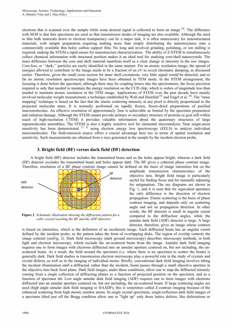
3. Bright field (BF) versus dark field (DF) detection
A bright field (BF) detector includes the transmitted beam and so the holes appear bright, whereas a dark field (DF) detector excludes the transmitted beam and holes appear dark. The BF gives a coherent phase contrast image. Therefore, resolution of a BF phase contrast image cannot be defined on the basis of image intensities but on the
amplitude transmission characteristics of the objective lens. Bright field image is particularly useful for finding focus and for manually adjusting for astigmatism. The ray diagrams are shown in Fig. 1, and it is seen that for equivalent apertures the only difference is the direction of electron propagation. Elastic scattering is the basis of phase contrast imaging, and depends only on scattering angle and not on propagation direction. In other words, the BF detector is small in angular extent compared to the diffraction angles, while the annular dark field (ADF) detector is large. A large detector, therefore, gives an image whose contrast
is based on intensities, which is the definition of an incoherent image. Each diffracted beam has an angular extent defined by the incident probe, so the pattern takes the form of overlapping disks. The region of overlap controls the image contrast (seeFig. 2). Dark field microscopy (dark ground microscopy) describes microscopy methods, in both light and electron microscopy, which exclude the un-scattered beam from the image. Annular dark field imaging requires one to form images with electrons diffracted into an annular aperture centered on, but not including, the un-scattered beam. As a result, the field around the specimen (i.e. where there is no specimen to scatter the beam) is generally dark. Dark field studies in transmission electron microscopy play a powerful role in the study of crystals and crystal defects, as well as in the imaging of individual atoms. Briefly, conventional dark field imaging involves tilting the incident illumination until a diffracted, rather than the incident, beam passes through a small objective aperture in the objective lens back focal plane. Dark field images, under these conditions, allow one to map the diffracted intensity coming from a single collection of diffracting planes as a function of projected position on the specimen, and as a function of specimen tilt. Low angle annular dark field imaging (ADF) requires one to form images with electrons diffracted into an annular aperture centered on, but not including, the un-scattered beam. If large scattering angles are used (high angle annular dark field imaging or HAADF), this is sometimes called Z-contrast imaging because of the enhanced scattering from high atomic number atoms. In single crystal specimens, single-reflection dark field images of a specimen tilted just off the Bragg condition allow one to "light up" only those lattice defects, like dislocations or
BF
detector
ADF
detector
Figure 2 Schematic illustration showing the diffraction pattern for a
cubic crystal reaching the BF and the ADF detectors
Microscopy: Science, Technology, Applications and Education A. Méndez-Vilas and J. Díaz (Eds.)
1890 ©FORMATEX 2010
______________________________________________

Figure 3 Dark field image with AlN 0002 reflection
broad based column due to local epitaxy
precipitates, which bend a single set of lattice planes in their neighborhood. Analysis of intensities in such images may then be used to estimate the amount of that bending. In polycrystalline specimens (Fig 3) dark field images serve to light up only that subset of crystals which is Bragg reflecting at a given orientation. The reason again is that changes in the interference pattern are on a local scale with respect to the ADF detector and are integrated by it. Only the changes in the total intensity falling on the detector affect the image. The thickness dependence of the Z-contrast image is therefore much simpler than that of a BF image. For instance, the reason that individual gold atoms cannot be located from the BF image alone is because of the speckle pattern contrast from the thin carbon film used to support the sample. The signal of a single gold atom cannot be distinguished from the support signal, whereas in a Z contrast image the single gold atom (Z = 79) scatters about as many electrons as the whole thickness of the carbon (Z = 6) support. Electrons scattered into high-angles are recorded with an annular detector. The cross-section for electrons scattered into high angles over a large angular range is roughly proportional to the squared atomic number of the scattering element. For large enough scattering angles, coherent effects between, e.g., atomic columns average out. Hence, the scattering process itself can be considered purely incoherent, which bypasses the phase problem that complicates interpretation of conventional high-resolution TEM using phase contrast imaging. High-angle annular dark field (HAADF) imaging is often referred to as Z-contrast imaging because of the atomic number dependence of the scattering cross-section. Consequently, the HAADF technique is most sensitive to heavy elements, and images provide a high degree of chemical information in addition to structural details. The advantage of the phase contrast image, on the other hand, is that it is more sensitive to light atoms. The ADF image clearly exhibits lattice contrast for the crystalline particles while the carbon support film is almost invisible due to the Z-dependence of the scattering cross-section and, therefore, the large contrast differences. The corresponding bright-field images, however, clearly show the typical speckle pattern for amorphous carbon, whose contrast depends on the defocus value during image acquisition. Furthermore, the BF images also reveal lattice information of the Au clusters but with different contrast when compared with the ADF images [9]. Additionally, since the electrons that are detected are incoherently scattered, phase contrast that produces the speckle pattern in bright field images of amorphous carbon is not present. As a result, single atoms can be imaged on the surface of an amorphous carbon film, and nanocrystal edges are clearly visible in cases where the nanocrystal is not susceptible to oxidation. These atoms and clusters would not be visible using conventional HRTEM since there is no contrast between amorphous materials and the amorphous carbon support.
Microscopy: Science, Technology, Applications and Education A. Méndez-Vilas and J. Díaz (Eds.)
©FORMATEX 2010 1891
______________________________________________

Condenser aperture
Electron source
Specimen
ADF detector
HAADF detector
BF detector
Figure 4 Schematic illustration of BF, ADF and
HAADF detectors in a STEM
Mainly, three types of detectors are used to obtain STEM images:
1.BF detector: It is placed at the same site as the aperture in BF-TEM and detects the intensity in the direct beam from a point on the specimen (see Fig. 4).
2. DF detector: The annular dark-field (ADF) detector is a disk with a hole in its center where the BF detector is installed. The ADF detector uses scattered electrons for image formation, similar to the DF (dark-field) mode in TEM. An annular dark field detector collects electrons from an annulus around the beam, sampling far more scattered electrons than can pass through an objective aperture. This gives an advantage in terms of signal collection efficiency and allows the main beam to pass to other detectors (EDX, EELS etc), allowing different types of measurement to be performed simultaneously. The measured contrast mainly results from electrons diffracted in crystalline areas but is superimposed by incoherent Rutherford scattering2.
3. HAADF detector: By using a STEM detector with a large inner radius, a HAADF detector, electrons are collected which are not Bragg scattered. As such HAADF images show little or no diffraction effects, and their intensity is approximately proportional to Z². This imaging technique proves ideal for tomographic reconstruction as it generates strong contrast that has a fully monotonic relationship with thickness. An annular dark field image formed only by very high angle, incoherently scattered3 electrons — as opposed to Bragg scattered electrons — is highly sensitive to variations in the atomic number of atoms in the sample (Z-contrast images). This technique is also known as high-angle
annular dark-field imaging (HAADF) [10]. The high-angle
annular dark field detector is also a disk with a hole, but the disk diameter and the hole are much larger than in the ADF detector. Thus, it detects electrons that are scattered to higher angles and almost only incoherent Rutherford scattering contributes to the image. Thereby, Z contrast is achieved.
Another important difference between BF and ADF imaging is the achievable resolution. Because of the influence of thermal vibrations, each successive electron can see the atoms in a slightly different position and the details of the pattern are different at high angles. The actual pattern from many scattering events looks diffuse, and the scattering is referred to as thermal diffuse scattering. Thermal effects actually assist in breaking the coherence of the ADF image. Image contrast requires interference, and the example of a crystal specimen shows clearly that for a crystal spacing the BF detector may see no interference because all the diffracted disks fall outside the detector. The atoms are too close to be resolved. The ADF detector, however, does see interference effects, and will show an image. In practice, the situation may be more complicated because the BF detector can see contrast formed as a result of multiple scattering. Sum and difference frequencies can appear giving spurious image features, and image simulations are important to interpret the complicated contrast effects that result. It seems obvious that in an incoherent image, the smaller the probe the better the resolution, or the sharper the atoms. This is true at present-day resolutions of around 0.6–1 Å, because the probe is still large compared to the region of the atom that scatters to high angles, which is just a few tens of an angstrom.
2 Rutherford scattering is also sometimes referred to as Coulomb scattering because it relies only upon static electric (Coulomb) forces, and the
minimal distance between particles is set only by this potential. 3 Scattering of particles or photons in which the scattering elements act independently of one another, so that there are no definite phase relationships
among the different parts of the scattered beam.
Microscopy: Science, Technology, Applications and Education A. Méndez-Vilas and J. Díaz (Eds.)
1892 ©FORMATEX 2010
______________________________________________

Methods Information
BF/ADF Detection of crystals, crystal defects and grain boundaries, phase analysis, particle size
HAADF Detection of small clusters or even single atoms of a heavy metal in a matrix of light elements (Z-contrast), direct visualization of structures and defects
4. Improving resolution
As the electron probe is sharpened, more of the probe strikes the target column and less is spread over neighboring columns. The smaller probe brings not only better spatial resolution but also more current on an individual column of atoms, resulting in a better signal-to-noise ratio and a higher sensitivity analysis. The ultimate sensitivity will become available for determining doping profiles, the influence of individual impurity atoms at a buried interface, and the nature of interface trap states. The spatial resolution of an STEM experiment is determined by the diameter of the electron probe. Therefore, the probe formation is the critical aspect determining interaction volumes inside the sample. To increase the spatial resolution, aberration correctors have recently been developed to overcome limitations due to lens imperfections and aberrations. Today, aberration-correction is successfully applied to both TEM and scanning transmission electron microscopy (STEM), and enables the discrimination of two objects separated by less than 1Å with both techniques. If a fine electron probe is used and the sample is a crystalline material oriented along one of its principal axes, individual columns of atoms can be imaged. In the following section, some basic concepts for aberration-correction will be reviewed.
4.1 Aberration correction
The aberration is an error in the optical path length between the actual wave front and the perfect sphere. Non-round aberrations, such as astigmatism4, introduce the dependence on the azimuthal angle. In practice, every optical lens exhibits aberrations. Lens aberrations can mainly be spheric or chromatic. Spheric (also referred to as geometric)
aberrations mean that rays traveling at an angle to the shortest line between sample and detector (optical axis) are focused at a different point to rays traveling almost parallel to that axis. Spheric aberrations cause electrons traveling at higher angles to the optical axis to be focused more strongly than those at smaller angles. This defines a Gaussian focus point. Spherical aberration is the most well-known geometric aberration because it was the dominant aberration before correction became possible. Chromatic
aberration is due to a spread in energy of the electron beam. They describe the spread in
focus of a lens dependent on the kinetic energy spread of the electron wave. Correcting the lens aberrations allows the objective aperture to be opened up, thereby obtaining higher resolution. At
the same time, as in an optical instrument like a camera, the depth of field5 is reduced. For high-resolution imaging the incident probe is a coherent spherical wave (slightly aberrated) that converges onto the specimen. It generates some scattered waves which propagate out of the specimen and onto the detectors. Most of these scattered waves remain coherent with the un-scattered beam, and will interfere with it. The traditional round magnetic lens has unavoidable aberrations that have limited the useful aperture that could be used, thus limiting resolution. Although it has long been known that multipole lenses could in principle be used to correct these aberrations, successful implementations of aberration correcting systems have only appeared in the past few years. The underlying principle used by aberration-correctors is to generate an identical but negative aberration coefficient, which cancels out with the one introduced by the actual lens itself. The fundamental strategy to achieve this has been laid out by Scherzer in 1947 when he proposed to break rotational symmetry to eliminate spherical and chromatic aberrations [11]. Consequently, non-round optical elements, so-called multipoles, have been used to facilitate aberration-correction for round lenses.
4 Astigmatism is a defect in which vision is blurred due to the inability of the optics to focus a point object into a sharp focused image. This may be
due to an irregular (scrape) or abnormal curvature of the lens 5 Although a lens can precisely focus at only one distance, the decrease in sharpness is gradual on each side of the focused distance, so that within the
DOF (depth of focus), the unsharpness is imperceptible under normal viewing conditions
Figure 5 Schematic illustrations showing the diffraction pattern for a cubic
crystal reaching the BF detector
Electron detector
Electron source
Spheric Chromatic
Lens
E-beam
Microscopy: Science, Technology, Applications and Education A. Méndez-Vilas and J. Díaz (Eds.)
©FORMATEX 2010 1893
______________________________________________

Z - scan
Figure 6 Specimen reconstructed at atomic
resolution in 3D
The initial goal of all efforts to correct lens aberrations in electron microscopy was to increase the spatial resolution, i.e. to decrease the electron probe diameter in the case of STEM. That this goal has been achieved is demonstrated with today’s sub-Ångström spatial resolution imaging conditions. In STEM, aberration-correction provides two additional effects: single atom sensitivity [12] and drastically increased depth sensitivity [13, 14]. As described above, ADF images are very sensitive to heavy elements since the scattering cross-section is roughly proportional to the squared atomic number of the illuminated species. However, bright field (BF) images, which are very sensitive to light elements in the sample, can be recorded simultaneously. Aberration-correction in STEM leads to ‘‘slower’’ oscillations of the phase contrast transfer function so that larger BF detectors can be used [15]. This directly results into BF images with enhanced signal when compared with the uncorrected case, which, according to the theorem of reciprocity, are equivalent to phase contrast images. Besides the smaller probe size, an additional advantage of aberration correction is that the STEM Bright Field (BF) has about two orders of magnitude more current, enhancing the signal-to-noise resolution.
4.2 Atomic resolution in 3D
Present-day aberration corrected STEMs have a depth of field of a few nanometers, and so it becomes possible to effectively depth slice through a sample and to reconstruct the set of images into a 3D representation of the structure. The technique is comparable to confocal optical microscopy, but provides a resolution that is on the nanoscale. Confocal imaging has revolutionized optical microscopy by facilitating 3D tomography through depth sectioning. ADF STEM is ideal for tomography since the images show no contrast reversals with focus. If the probe-forming aperture is doubled again, to 50 mrad or above, then most of the probe intensity is contained in the high angle components of the probe. With a small aperture, the crystal lattice could be imaged in projection, while 3D tomography could be achieved with a larger aperture. Furthermore, EELS data or X-ray fluorescence data could also be collected and reconstructed in 3D, providing the ultimate analysis: 3D reconstruction at atomic resolution with single atom identification.
Aberration correction provides the increased spatial resolution by allowing the objective lens aperture to be increased. Just as in a camera, this results in a reduced depth of field. In fact, the depth of field dz
decreases as the square of the aperture angle, whereas the lateral resolution, which has been the main motivation for aberration correction, increases only linearly with aperture angle. Depth resolution on the 300-kV STEM today is on the nanometer scale, and we can optically slice through a sample simply by changing the objective lens focus. A through-focal series now becomes a through-depth series, which can be recombined into a 3D data set [16] in a similar manner as used for confocal optical microscopy. However, the electron technique retains single-atom sensitivity in each image if the specimen is sufficiently thin. A resulting consequence is that STEM data can no longer be interpreted as a simple two-dimensional projection of a three-dimensional structure, but provides three dimensional information with the ultimate sensitivity down to one single atom.
Also, there are major advantages in increasing the accelerating voltage. Increased specimen penetration means that thicker specimens can be tolerated; but more importantly, the decreasing electron wavelength leads to higher spatial resolution and the ability to see the actual atomic configurations within the nanostructure.
5. Other measurements
In STEM, multiple detectors can be used simultaneously to give different views of the sample, providing
different but complementary information. The beam can be localized on a certain point in the image and used to measure an Energy-Dispersive X-ray Spectroscopy (EDXS) and/or Electron Energy Loss Spectroscopy (EELS) spectrum at there. Moreover, line scans and mappings can be obtained by this powerful technique. At each spot, the generated signal is simultaneously recorded by selected detectors, building up an image. Other detectors are also possible; secondary electrons, cathodoluminescence, or electron beam-induced current can all be used to form an image. In optical materials, a particularly useful signal is the cathodoluminescence generated by the electron beam. Using an optical detection system, the light generated as the beam scans can be collected simultaneously with the ADF image to form a map showing the optical emission. However, these signals tend to be lower in intensity and therefore may be insufficient to form a clear, high-resolution image of a nanostructure in a reasonable exposure time. Typically, one would image a nanostructure using the high-intensity transmitted electron detector, then stop the beam on the nanostructure for detection of x-rays or EELS data. Alternatively, one may be able to scan with a larger, higher current beam to obtain sufficient signal-to-noise ratio in some weaker signal of interest, sacrificing spatial resolution. Low-loss features in the energy loss spectrum or low-energy core loss edges are particularly useful in this regard. One of the
Microscopy: Science, Technology, Applications and Education A. Méndez-Vilas and J. Díaz (Eds.)
1894 ©FORMATEX 2010
______________________________________________
advantages of a scanning microscope is that any signal can be monitored as a function of probe position and used to form an image.
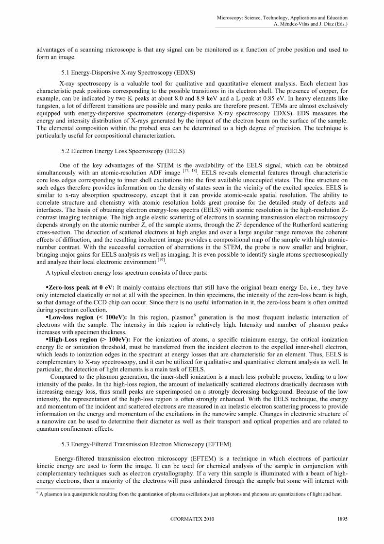
5.1 Energy-Dispersive X-ray Spectroscopy (EDXS)
X-ray spectroscopy is a valuable tool for qualitative and quantitative element analysis. Each element has characteristic peak positions corresponding to the possible transitions in its electron shell. The presence of copper, for example, can be indicated by two K peaks at about 8.0 and 8.9 keV and a L peak at 0.85 eV. In heavy elements like tungsten, a lot of different transitions are possible and many peaks are therefore present. TEMs are almost exclusively equipped with energy-dispersive spectrometers (energy-dispersive X-ray spectroscopy EDXS). EDS measures the energy and intensity distribution of X-rays generated by the impact of the electron beam on the surface of the sample. The elemental composition within the probed area can be determined to a high degree of precision. The technique is particularly useful for compositional characterization.
5.2 Electron Energy Loss Spectroscopy (EELS)
One of the key advantages of the STEM is the availability of the EELS signal, which can be obtained simultaneously with an atomic-resolution ADF image [17, 18]. EELS reveals elemental features through characteristic core loss edges corresponding to inner shell excitations into the first available unoccupied states. The fine structure on such edges therefore provides information on the density of states seen in the vicinity of the excited species. EELS is similar to x-ray absorption spectroscopy, except that it can provide atomic-scale spatial resolution. The ability to correlate structure and chemistry with atomic resolution holds great promise for the detailed study of defects and interfaces. The basis of obtaining electron energy-loss spectra (EELS) with atomic resolution is the high-resolution Z-contrast imaging technique. The high angle elastic scattering of electrons in scanning transmission electron microscopy depends strongly on the atomic number Z, of the sample atoms, through the Z² dependence of the Rutherford scattering cross-section. The detection of scattered electrons at high angles and over a large angular range removes the coherent effects of diffraction, and the resulting incoherent image provides a compositional map of the sample with high atomic-number contrast. With the successful correction of aberrations in the STEM, the probe is now smaller and brighter, bringing major gains for EELS analysis as well as imaging. It is even possible to identify single atoms spectroscopically and analyze their local electronic environment [19].
A typical electron energy loss spectrum consists of three parts: �Zero-loss peak at 0 eV: It mainly contains electrons that still have the original beam energy Eo, i.e., they have
only interacted elastically or not at all with the specimen. In thin specimens, the intensity of the zero-loss beam is high, so that damage of the CCD chip can occur. Since there is no useful information in it, the zero-loss beam is often omitted during spectrum collection.
�Low-loss region (< 100eV): In this region, plasmon6 generation is the most frequent inelastic interaction of electrons with the sample. The intensity in this region is relatively high. Intensity and number of plasmon peaks increases with specimen thickness.
�High-Loss region (> 100eV): For the ionization of atoms, a specific minimum energy, the critical ionization energy Ec or ionization threshold, must be transferred from the incident electron to the expelled inner-shell electron, which leads to ionization edges in the spectrum at energy losses that are characteristic for an element. Thus, EELS is complementary to X-ray spectroscopy, and it can be utilized for qualitative and quantitative element analysis as well. In particular, the detection of light elements is a main task of EELS.
Compared to the plasmon generation, the inner-shell ionization is a much less probable process, leading to a low intensity of the peaks. In the high-loss region, the amount of inelastically scattered electrons drastically decreases with increasing energy loss, thus small peaks are superimposed on a strongly decreasing background. Because of the low intensity, the representation of the high-loss region is often strongly enhanced. With the EELS technique, the energy and momentum of the incident and scattered electrons are measured in an inelastic electron scattering process to provide information on the energy and momentum of the excitations in the nanowire sample. Changes in electronic structure of a nanowire can be used to determine their diameter as well as their transport and optical properties and are related to quantum confinement effects.
5.3 Energy-Filtered Transmission Electron Microscopy (EFTEM)
Energy-filtered transmission electron microscopy (EFTEM) is a technique in which electrons of particular kinetic energy are used to form the image. It can be used for chemical analysis of the sample in conjunction with complementary techniques such as electron crystallography. If a very thin sample is illuminated with a beam of high-energy electrons, then a majority of the electrons will pass unhindered through the sample but some will interact with 6 A plasmon is a quasiparticle resulting from the quantization of plasma oscillations just as photons and phonons are quantizations of light and heat.
Microscopy: Science, Technology, Applications and Education A. Méndez-Vilas and J. Díaz (Eds.)
©FORMATEX 2010 1895
______________________________________________
the sample, being scattered elastically or inelastically (phonon scattering, plasmon scattering or inner shell ionisation). Inelastic scattering results in both a loss of energy and a change in momentum, which in the case of inner shell ionisation is characteristic of the element in the sample. If the electron beam emerging from the sample is passed through a magnetic prism, then the flight path of the electrons will vary depending on their energy. This technique is used to form spectra in electron energy loss spectroscopy (EELS), but it is also possible to place an adjustable slit to allow only electrons with a certain range of energies through, and reform an image using these electrons on a detector. The energy slit can be adjusted so as to only allow electrons which have not lost energy to pass through to form the image. This prevents inelastic scattering from contributing to the image, and hence produces an enhanced contrast image. Adjusting the slit to only allow electrons which have lost a specific amount of energy can be used to obtain elementally sensitive images. As the ionisation signal is often significantly smaller than the background signal, it is normally necessary to obtain more than one image at varying energies to remove the background effect.
Acknowledgements The support by Ministerio de Ciencia e Innovacion Project W050920B0 is gratefully acknowledged.
References
[1] S. J. Pennycook, M. Varela, C. J. D. Hetherington, A. I. Kirkland, 2006, MRS Bull, 31, 36. [2] L. Reimer, 1992, Diagnostics and Applications of Thin Films, 1. [3] R. J. Potton, 2004, Reports on Progress in Physics, 67, 717. [4] A. V. Crewe, J. Wall, J. Langmore, 1970, Science, 168, 1338. [5] J. S. Wall, M. N. Simon, J. F. Hainfeld, 2009, Advances in Imaging and Electron Physics, Vol 159, 159, 101. [6] A. Engel, W. Baumeister, W. O. Saxton, 1982, Proceedings of the National Academy of Sciences of the United States of America-
Biological Sciences, 79, 4050. [7] R. D. Leapman, 2004, Curr. Opin. Neurobiol., 14, 591. [8] R. D. Leapman, 2003, Journal of Microscopy-Oxford, 210, 5. [9] L. Gontard, R. Dunin-Borkowski, M. Gass, A. Bleloch, D. Ozkaya, 2009, J. Electron Microsc., 58, 167. [10] P. Midgley, M. Weyland, 2003, Ultramicroscopy, 96, 413. [11] O. SCHERZER, 1947, Optik, 2, 114. [12] S. W. Wang, A. Y. Borisevich, S. N. Rashkeev, M. V. Glazoff, K. Sohlberg, S. J. Pennycook, S. T. Pantelides, 2004, Nature
Materials, 3, 274. [13] A. Y. Borisevich, A. R. Lupini, S. Travaglini, S. J. Pennycook, 2006, J. Electron Microsc., 55, 7. [14] K. van Benthem, A. R. Lupini, M. Kim, H. S. Baik, S. Doh, J. H. Lee, M. P. Oxley, S. D. Findlay, L. J. Allen, J. T. Luck, S. J.
Pennycook, 2005, Appl. Phys. Lett., 87. [15] M. Varela, A. Lupini, K. van Benthem, A. Borisevich, M. Chisholm, N. Shibata, 2005, Annual review of materials research, 35,
539. [16] A. Viezzoli, A. Christiansen, E. Auken, K. Sorensen, 2008, Geophysics, 73, F105. [17] N. D. Browning, M. F. Chisholm, S. J. Pennycook, 1993, Nature, 366, 143. [18] P. E. Batson, N. Dellby, O. L. Krivanek, 2002, Nature, 418, 617. [19] M. Varela, S. Findlay, A. Lupini, H. Christen, A. Borisevich, N. Dellby, 2004, Phys. Rev. Lett., 92.
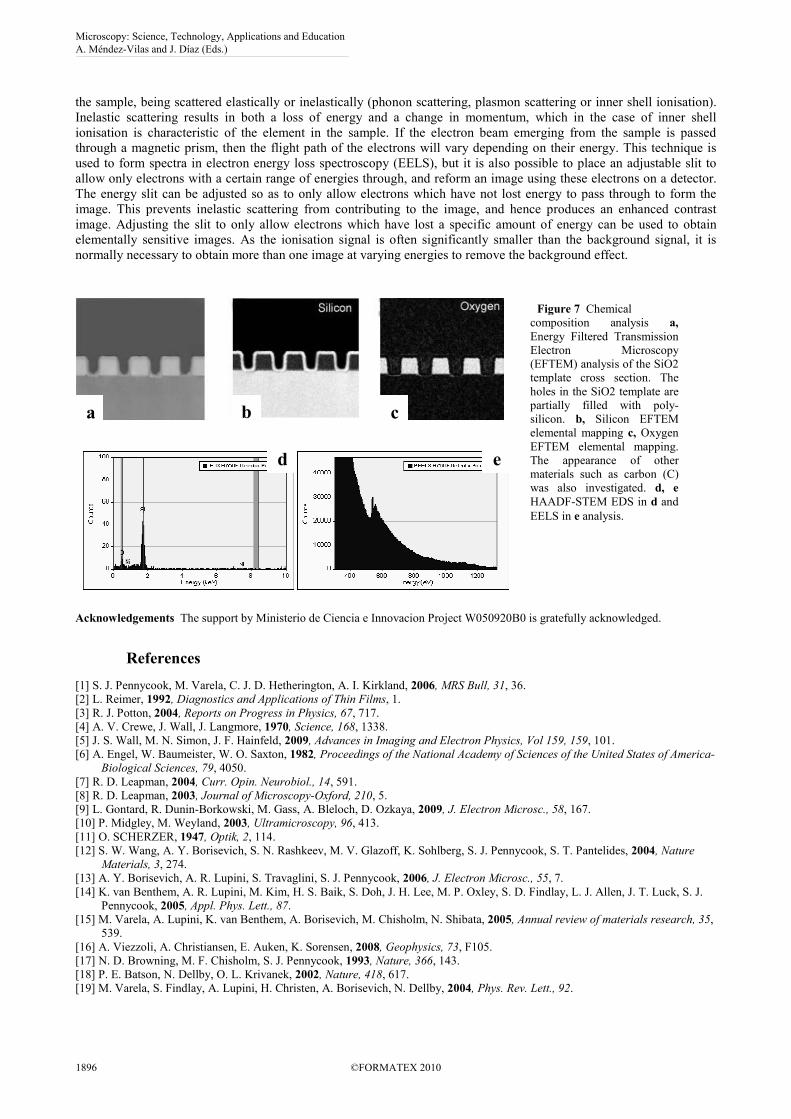
Figure 7 Chemical composition analysis a,
Energy Filtered Transmission Electron Microscopy (EFTEM) analysis of the SiO2 template cross section. The holes in the SiO2 template are partially filled with poly-silicon. b, Silicon EFTEM elemental mapping c, Oxygen EFTEM elemental mapping. The appearance of other materials such as carbon (C) was also investigated. d, e HAADF-STEM EDS in d and EELS in e analysis.
e d
a b c
Microscopy: Science, Technology, Applications and Education A. Méndez-Vilas and J. Díaz (Eds.)
1896 ©FORMATEX 2010
______________________________________________
![Electron Microscopy - Wikis09-10]_DOWNLOAD/4 tem i.… · Electron Microscopy 4. TEM Basics: interactions, basic modes, sample preparation, Diffraction: elastic scattering theory,](https://static.fdocuments.us/doc/165x107/5f05009e7e708231d410c617/electron-microscopy-wikis-09-10download4-tem-i-electron-microscopy-4-tem.jpg)