Training Course (I) - nstg.nevada.edunstg.nevada.edu/tem/training_course/tem-training... ·...
49
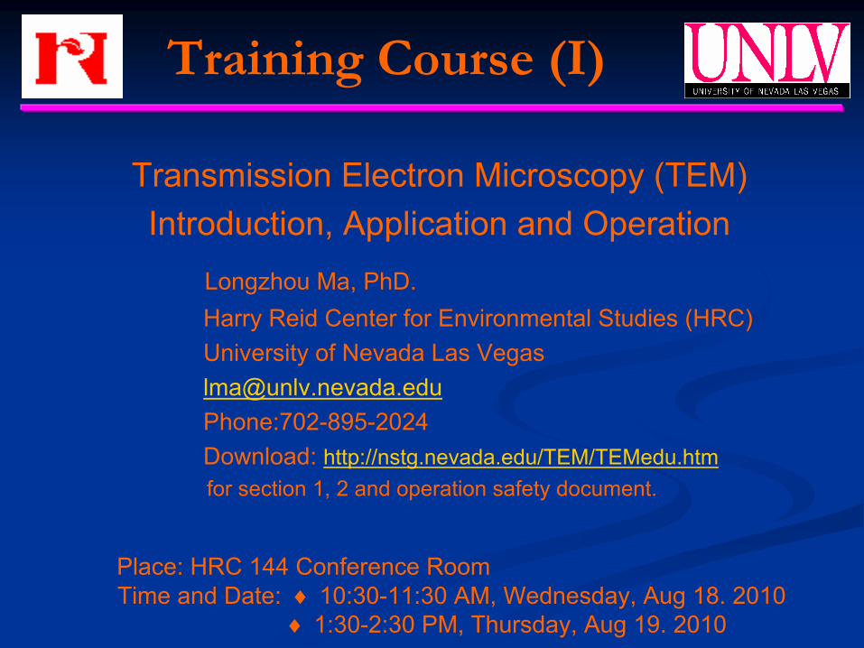
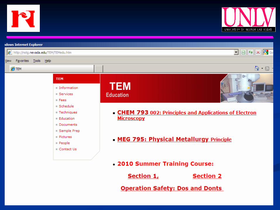
Transmission Electron Microscopy (TEM) Introduction, Application and Operation Longzhou Ma, PhD. Harry Reid Center for Environmental Studies (HRC) University of Nevada Las Vegas [email protected] Phone:702-895-2024 Download: http://nstg.nevada.edu/TEM/TEMedu.htm for section 1, 2 and operation safety document. Place: HRC 144 Conference Room Time and Date: ♦ 10:30-11:30 AM, Wednesday, Aug 18. 2010 ♦ 1:30-2:30 PM, Thursday, Aug 19. 2010 Training Course (I)
Transcript of Training Course (I) - nstg.nevada.edunstg.nevada.edu/tem/training_course/tem-training... ·...
Transmission Electron Microscopy (TEM) Introduction, Application and Operation
Longzhou Ma, PhD.Harry Reid Center for Environmental Studies (HRC)University of Nevada Las [email protected]:702-895-2024Download: http://nstg.nevada.edu/TEM/TEMedu.htmfor section 1, 2 and operation safety document.
Place: HRC 144 Conference RoomTime and Date: ♦ 10:30-11:30 AM, Wednesday, Aug 18. 2010
♦ 1:30-2:30 PM, Thursday, Aug 19. 2010
Training Course (I)
TEM BasicsTEM Basics
TEM Image Mode TEM Image Mode
InIn--situ TEMsitu TEM
TECNAI-F30 Super-twin TEM Components, Interfaces and Operations
Sample Preparation
Outline
TEM Basics
TEM Image Mode
In-situ TEM
Part I
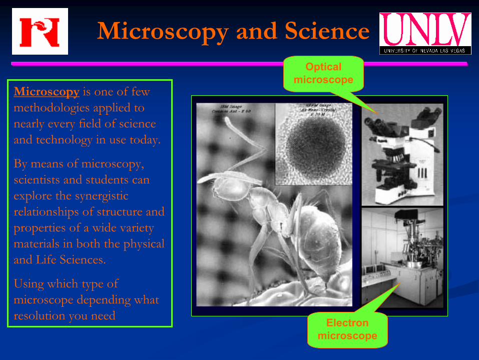
Microscopy is one of few methodologies applied to nearly every field of science and technology in use today.
By means of microscopy, scientists and students can explore the synergistic relationships of structure and properties of a wide variety materials in both the physical and Life Sciences.
Using which type of microscope depending what resolution you need
Optical microscope
Electron microscope
Microscopy and Science
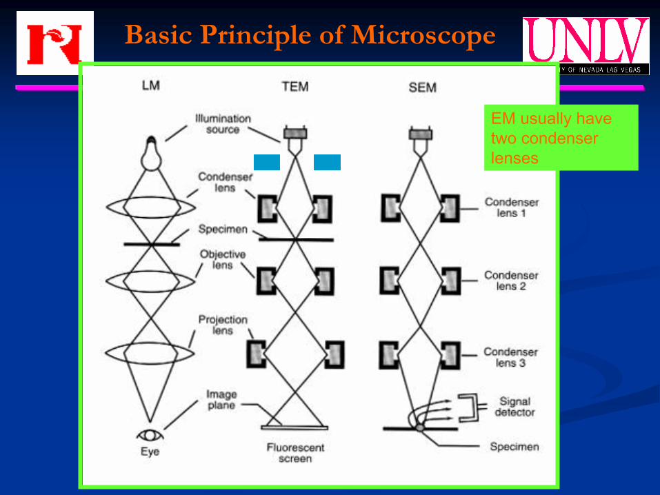
Basic Principle of Microscope
EM usually have two condenser lenses
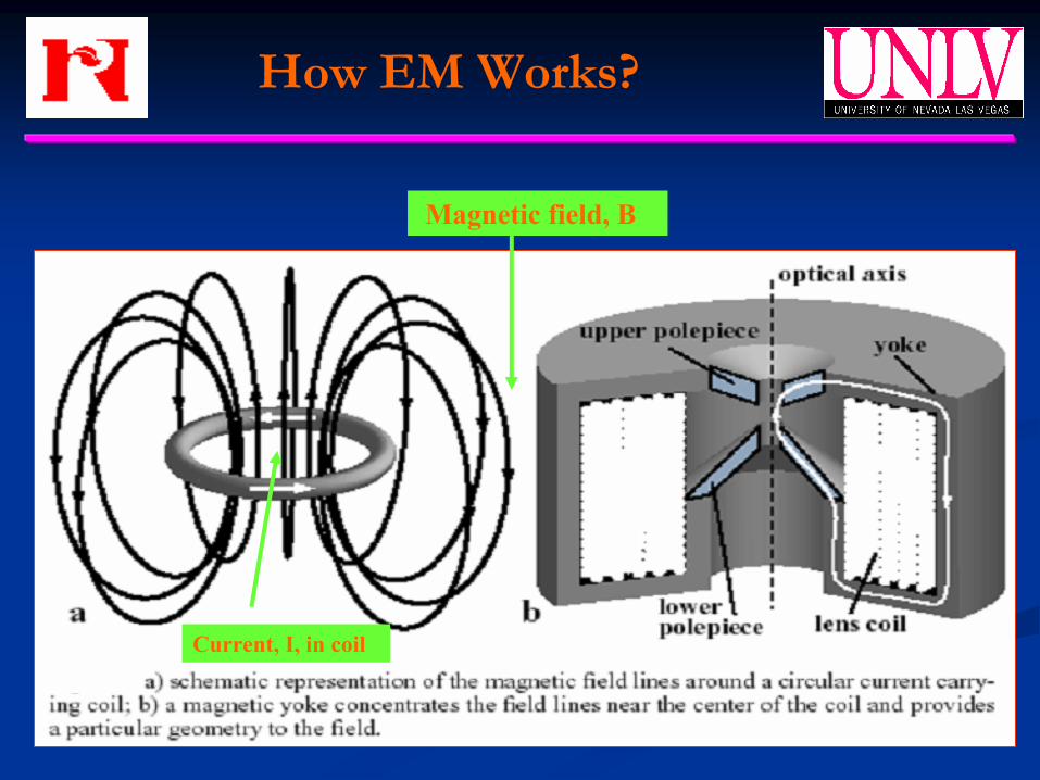
Current, I, in coil
Magnetic field, B
How EM Works?
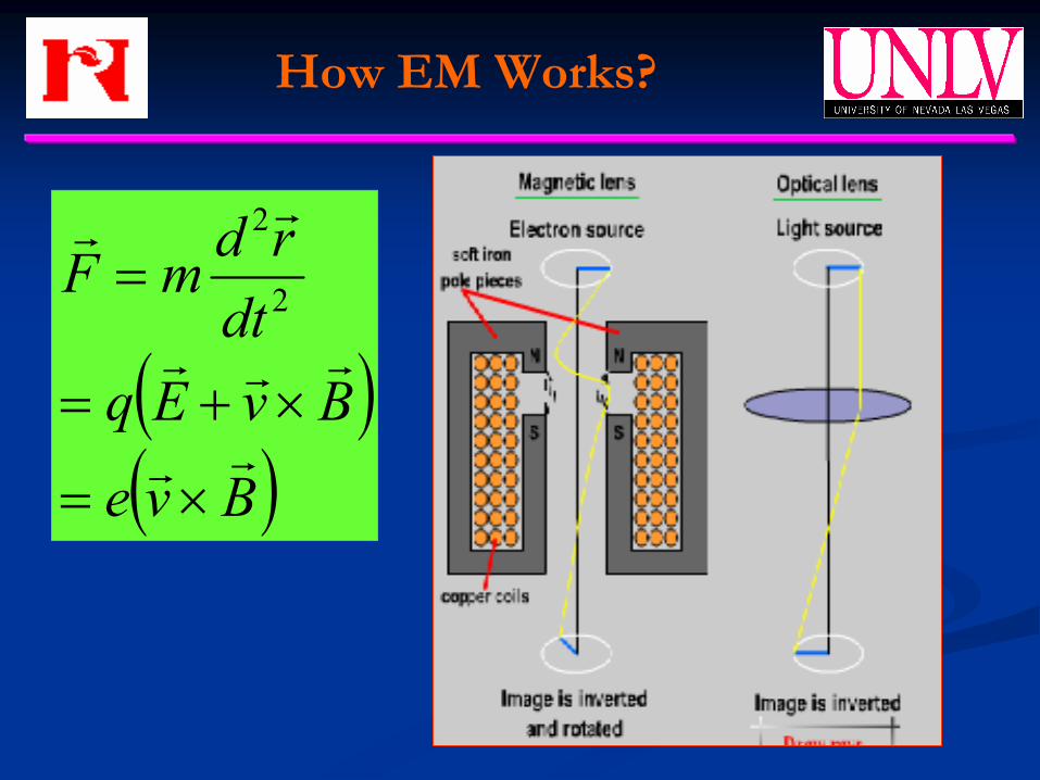
( )( )Bve
BvEqdtrdmF
rr
rrr
rr
×=
×+=
= 2
2
How EM Works?
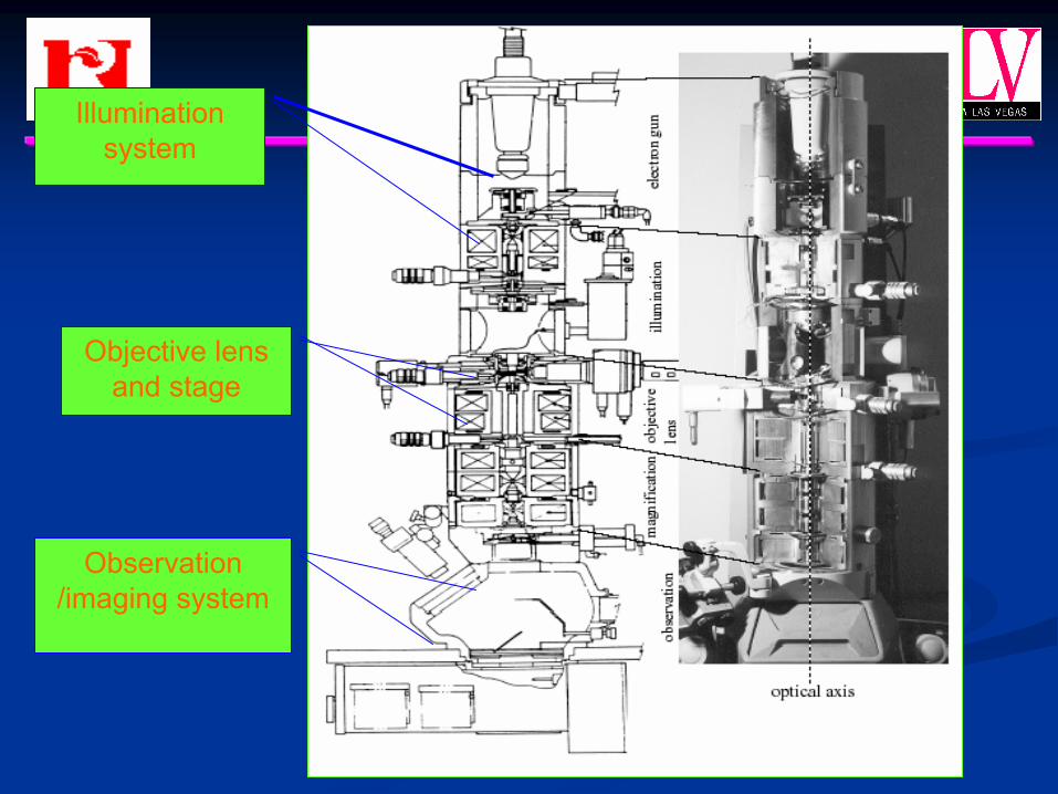
Illumination system
Objective lens and stage
Observation /imaging system
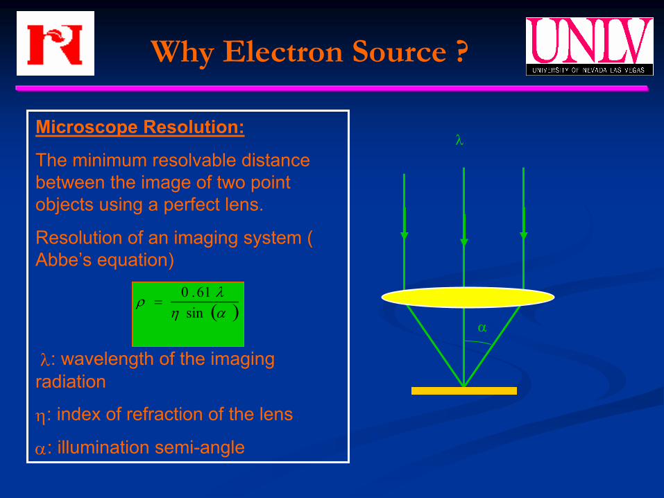
Microscope Resolution:
The minimum resolvable distance between the image of two point objects using a perfect lens.
Resolution of an imaging system ( Abbe’s equation)
λ: wavelength of the imaging radiation
η: index of refraction of the lens
α: illumination semi-angle
α
λ
( )αηλρ
sin61.0
=
Why Electron Source ?
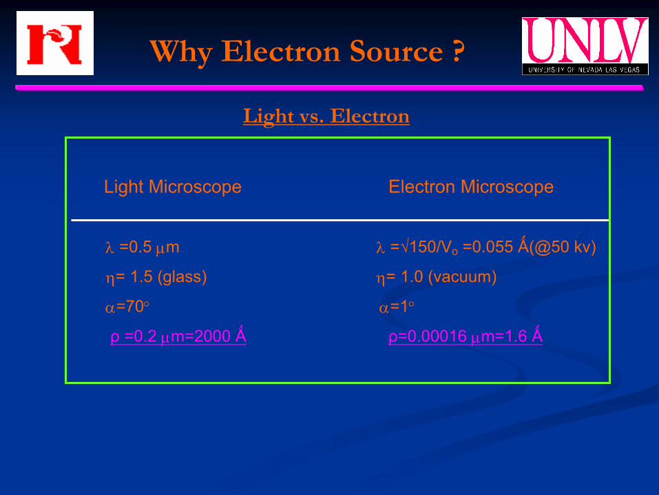
Light vs. Electron
Light Microscope Electron Microscope
λ =0.5 µm λ =√150/Vo =0.055 Ǻ(@50 kv)
η= 1.5 (glass) η= 1.0 (vacuum)
α=70° α=1°
ρ =0.2 µm=2000 Ǻ ρ=0.00016 µm=1.6 Ǻ
Why Electron Source ?
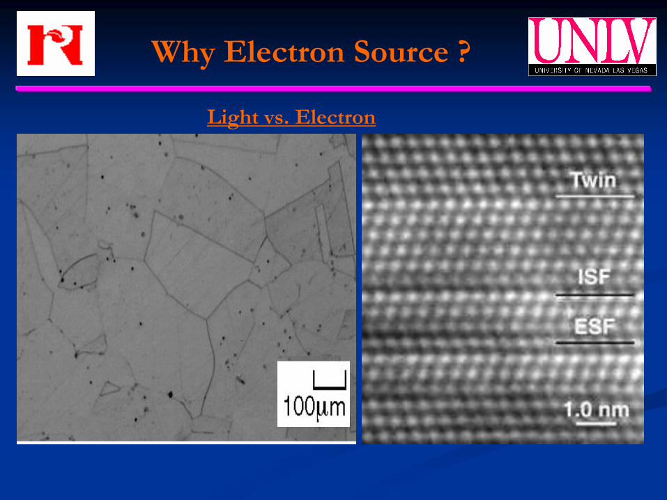
Light vs. Electron
Why Electron Source ?
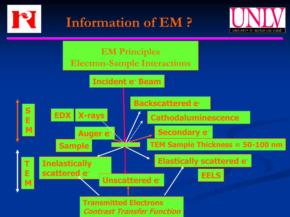
Information of EM ?
EM PrinciplesElectron-Sample Interactions
Incident e- Beam
Backscattered e-
Auger e- Secondary e-
Inelasticallyscattered e-
Unscattered e-
Elastically scattered e-
Transmitted ElectronsContrast Transfer Function
X-rays Cathodaluminescence
Sample TEM Sample Thickness = 50-100 nm
EDX
EELS
SEM
TEM
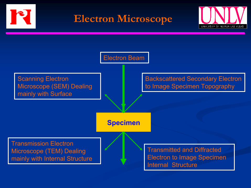
Electron Microscope
Specimen
Scanning Electron Microscope (SEM) Dealing mainly with Surface
Electron Beam
Backscattered Secondary Electron to Image Specimen Topography
Transmission Electron Microscope (TEM) Dealing mainly with Internal Structure
Transmitted and Diffracted Electron to Image Specimen Internal Structure
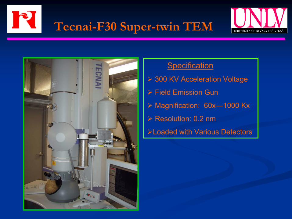
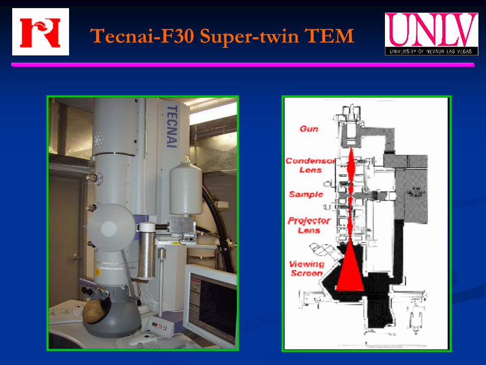
Tecnai-F30 Super-twin TEM
Specification300 KV Acceleration Voltage
Field Emission Gun
Magnification: 60x—1000 Kx
Resolution: 0.2 nm
Loaded with Various Detectors
Tecnai-F30 Super-twin TEM
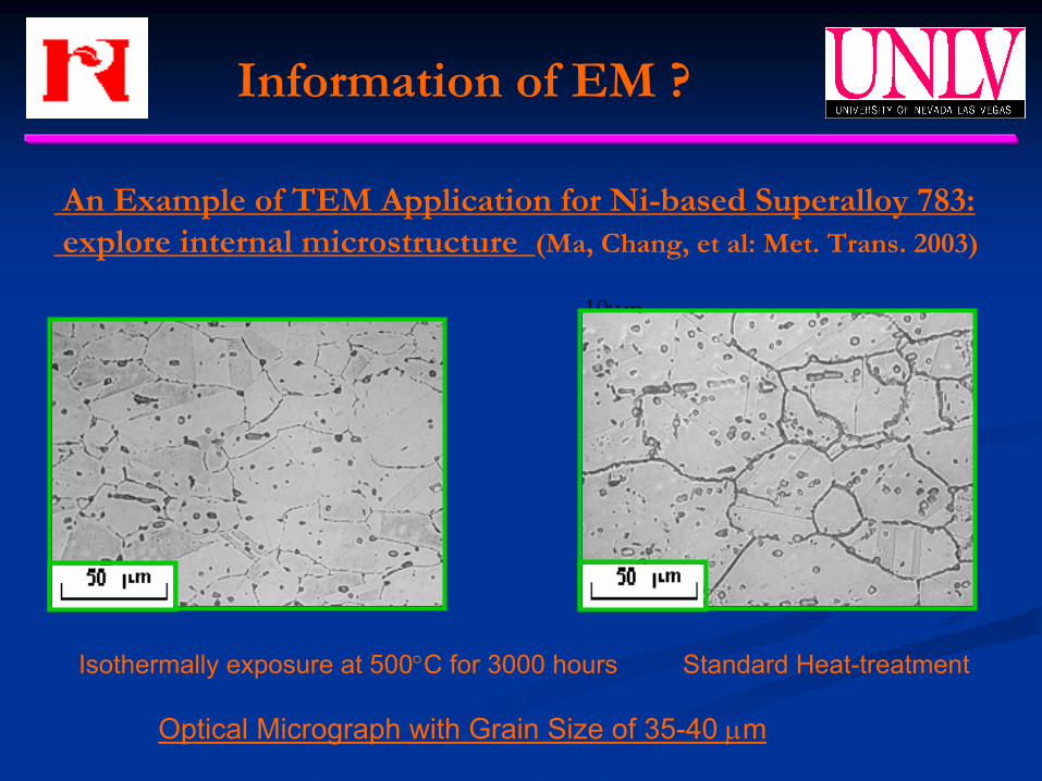
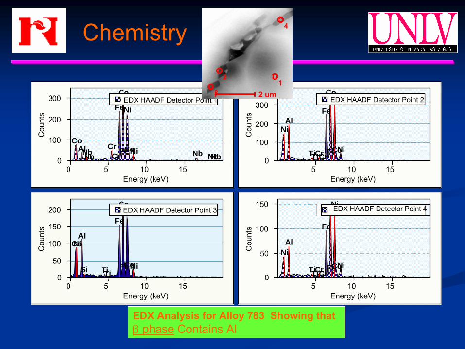
An Example of TEM Application for Ni-based Superalloy 783: explore internal microstructure (Ma, Chang, et al: Met. Trans. 2003)
10µm
Isothermally exposure at 500°C for 3000 hours Standard Heat-treatment
Optical Micrograph with Grain Size of 35-40 µm
Information of EM ?
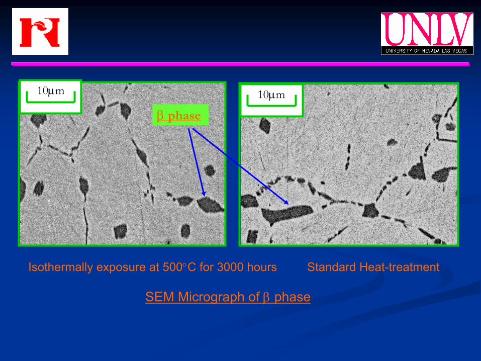
10µm 10µm 10µm 10µm
Isothermally exposure at 500°C for 3000 hours Standard Heat-treatment
SEM Micrograph of β phase
β phase
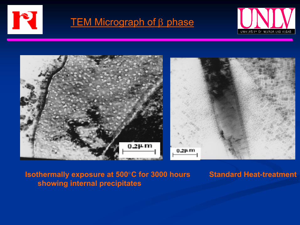
Isothermally exposure at 500°C for 3000 hours Standard Heat-treatmentshowing internal precipitates
TEM Micrograph of β phase
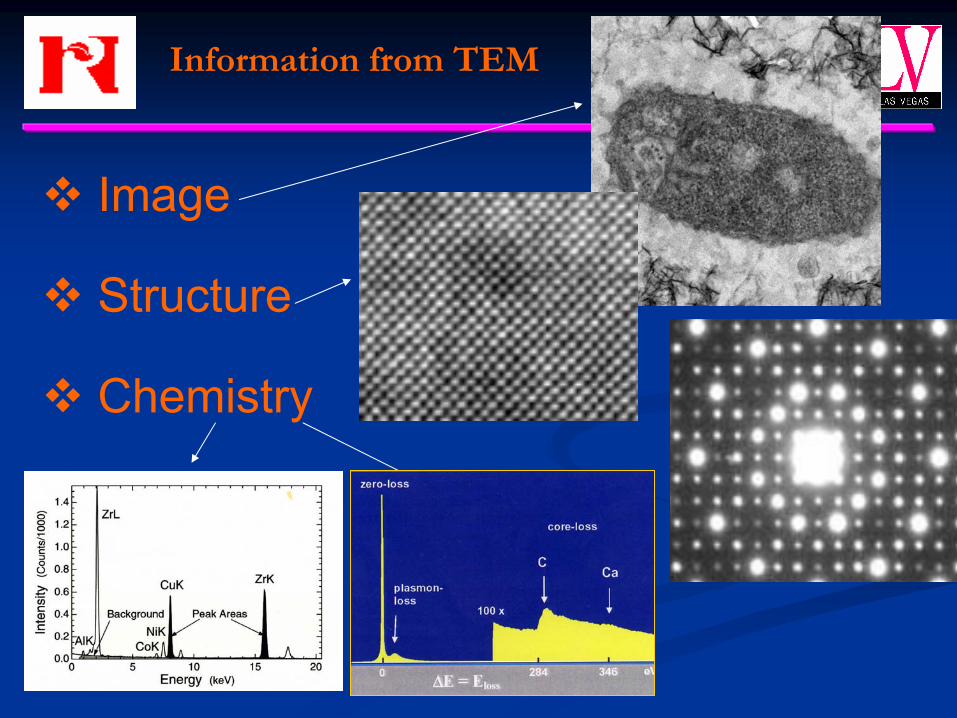
Information from TEM
Image
Structure
Chemistry
Image contrast tells information
Morphology and Dimension
Defects and Microstructures
Image
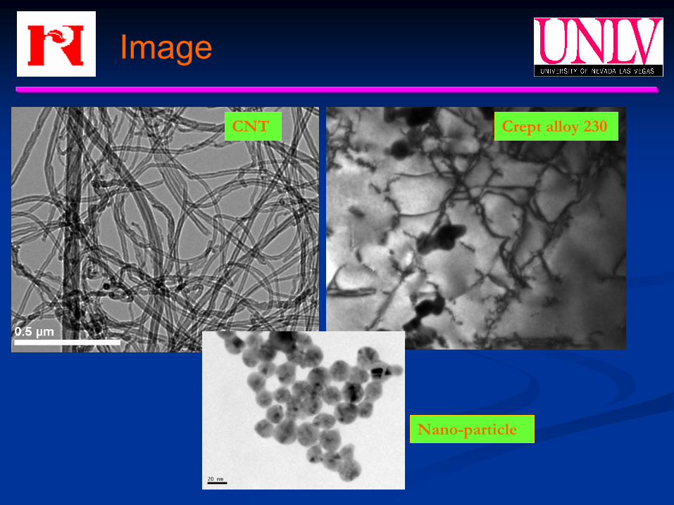
Image
CNT Crept alloy 230
Nano-particle
Structure
FFTFFT 2Th Degrees80706050403020
Sqr
t(Cou
nts)
500
450
400
350
300
250
200
150
100
50
0
-50
Si-SRM 640c 14.75 %Cryptomelane 85.25 %*
**
* * *
*
6.99
Å (1
10)
4.94
Å (0
20)
3.13
Å (3
10)
2.40
Å (2
11)
2.16
Å (0
31)
1.84
Å (4
11)
1.54
Å (2
51)
2 Theta (°)2Th Degrees80706050403020
Sqr
t(Cou
nts)
500
450
400
350
300
250
200
150
100
50
0
-50
Si-SRM 640c 14.75 %Cryptomelane 85.25 %*
**
* * *
*
6.99
Å (1
10)
4.94
Å (0
20)
3.13
Å (3
10)
2.40
Å (2
11)
2.16
Å (0
31)
1.84
Å (4
11)
1.54
Å (2
51)
2 Theta (°)
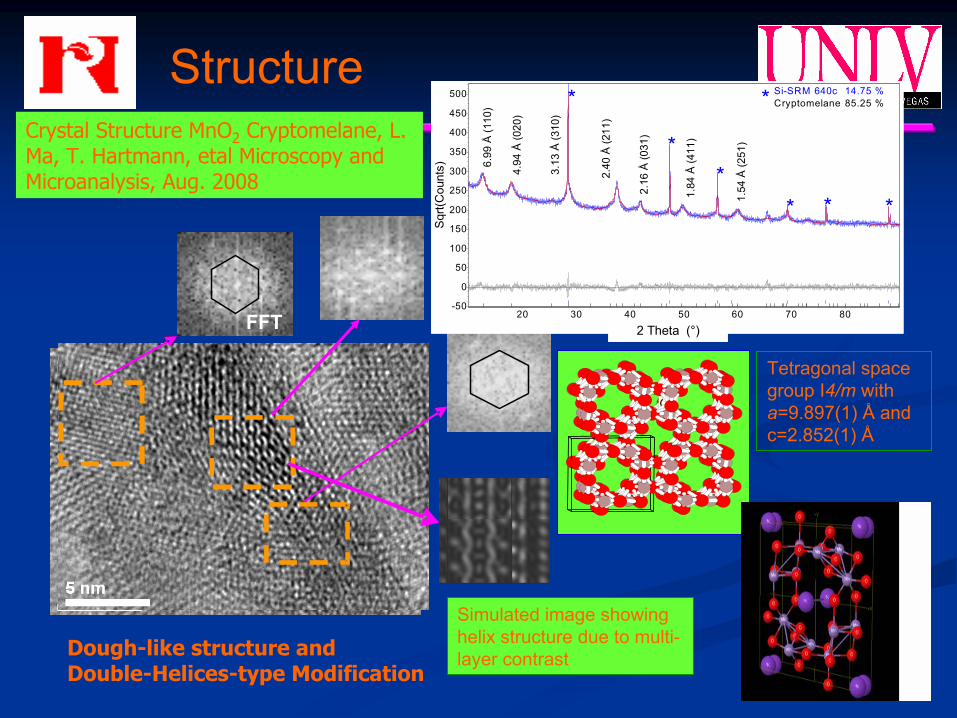
Crystal Structure MnO2 Cryptomelane, L. Ma, T. Hartmann, etal Microscopy and Microanalysis, Aug. 2008
Dough-like structure and Double-Helices-type Modification
O2
Tetragonal space group I4/m witha=9.897(1) Å and c=2.852(1) Å
Simulated image showing helix structure due to multi-layer contrast
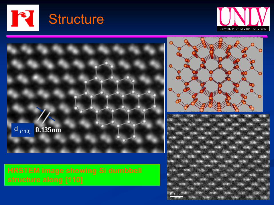
Structure
HRSTEM image showing Si dumbbell structure along [110]
d (110)
Chemistry
Energy (keV)
Cou
nts
151050
200
150
100
50
0
Al
Si
Co
Co
Co
Ni
Ni
Ni
TiTi
Fe
Fe
EDX HAADF Detector Point 3
Energy (keV)
Cou
nts
151050
300
200
100
0Al Cr
Cr
Fe
Fe
Ni
Ni Nb NbNbNbNb
Co
CoCo
EDX HAADF Detector Point 1
Energy (keV)
Cou
nts
15105
300
200
100
0
AlFe
Fe
Ni
Ni
Ni
TiTiCrCr
Co
Co
EDX HAADF Detector Point 2
Energy (keV)
Cou
nts
15105
150
100
50
0
Al
Fe
Fe
Ni
Ni
Ni
TiTiCrCr
Co
Co
EDX HAADF Detector Point 4
EDX Analysis for Alloy 783 Showing that β phase Contains Al
2 um1
2
3
4
Chemistry
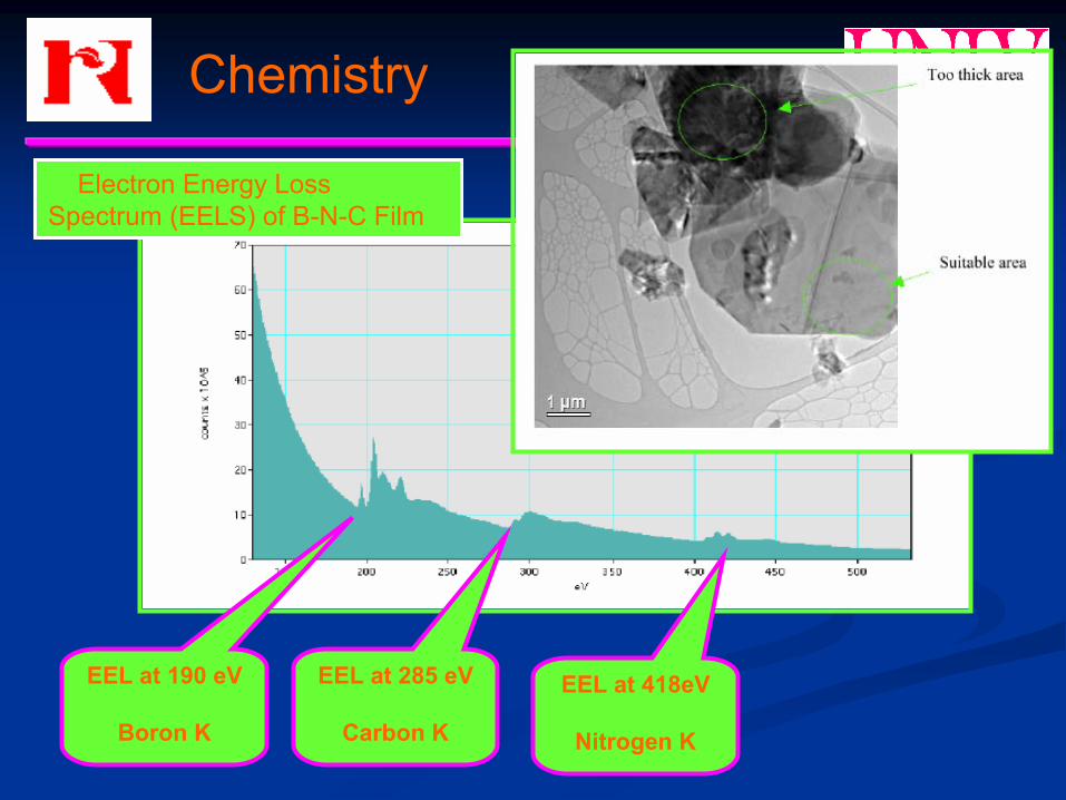
EEL at 190 eV
Boron K
EEL at 285 eV
Carbon K
EEL at 418eV
Nitrogen K
Electron Energy Loss Spectrum (EELS) of B-N-C Film
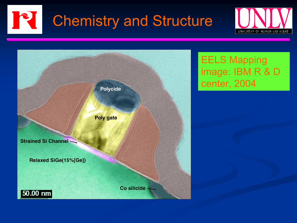
Chemistry and Structure
EELS Mapping image: IBM R & D center, 2004
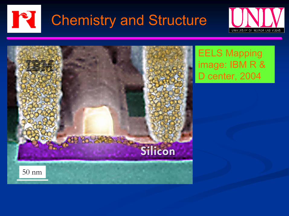
Chemistry and Structure
EELS Mapping image: IBM R & D center, 2004
50 nm
TEM Image Mode
TEM Modes
Bright Field Image Mode
Dark Field Image Mode
Diffraction Mode
HRTEM Mode
STEM and Analysis Mode
In-situ TEM
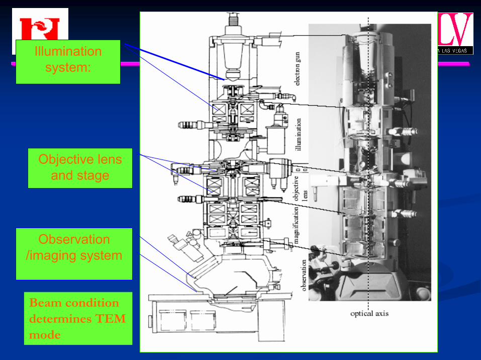
Illumination system:
Objective lens and stage
Observation /imaging system
Beam condition determines TEM mode
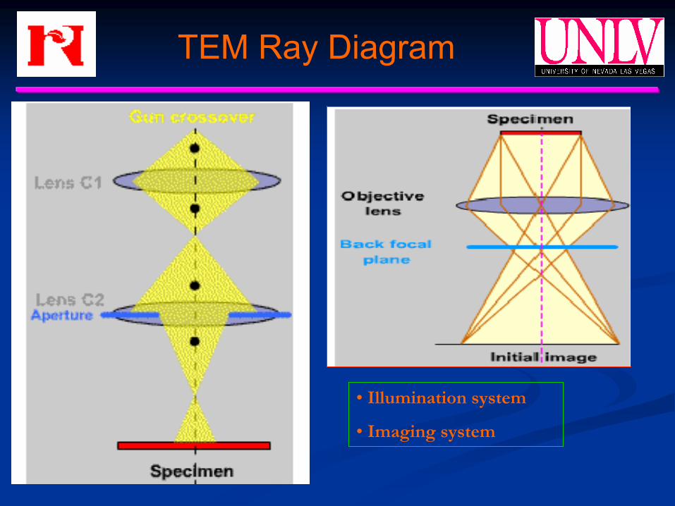
TEM Ray Diagram
• Illumination system
• Imaging system
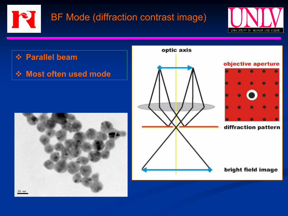
BF Mode (diffraction contrast image)
Parallel beam
Most often used mode
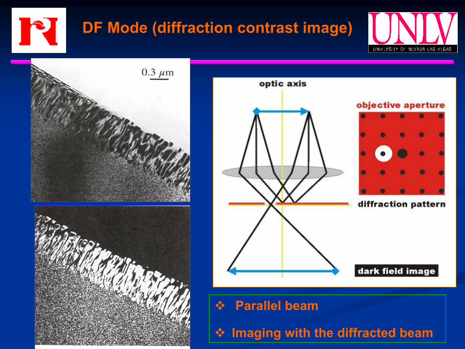
Parallel beam
Imaging with the diffracted beam
DF Mode (diffraction contrast image)
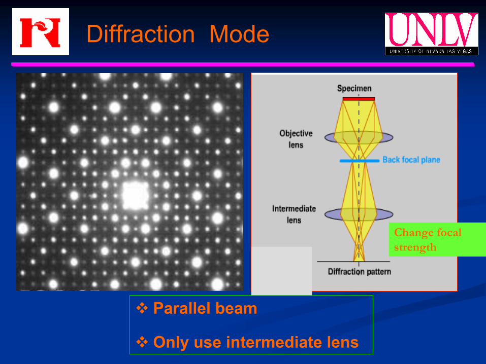
Diffraction Mode
Parallel beam
Only use intermediate lens
Change focal strength
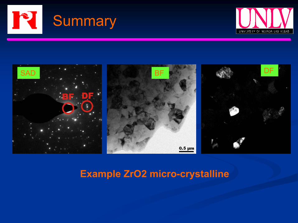
Summary
Example ZrO2 micro-crystalline
BF DFSAD
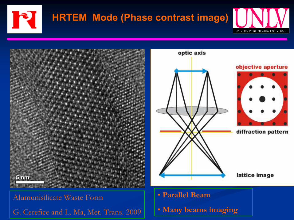
HRTEM Mode (Phase contrast image)
Alumunisilicate Waste Form
G. Cerefice and L. Ma, Met. Trans. 2009
• Parallel Beam
• Many beams imaging
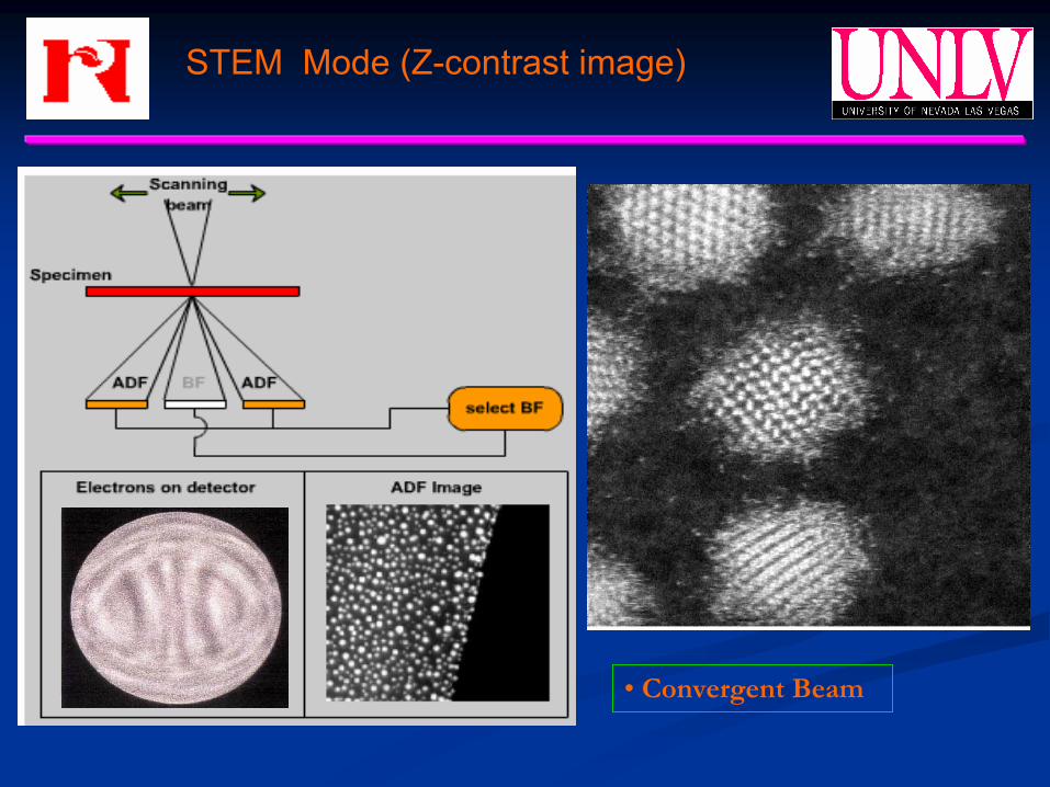
STEM Mode (Z-contrast image)
• Convergent Beam
Convergent Beam
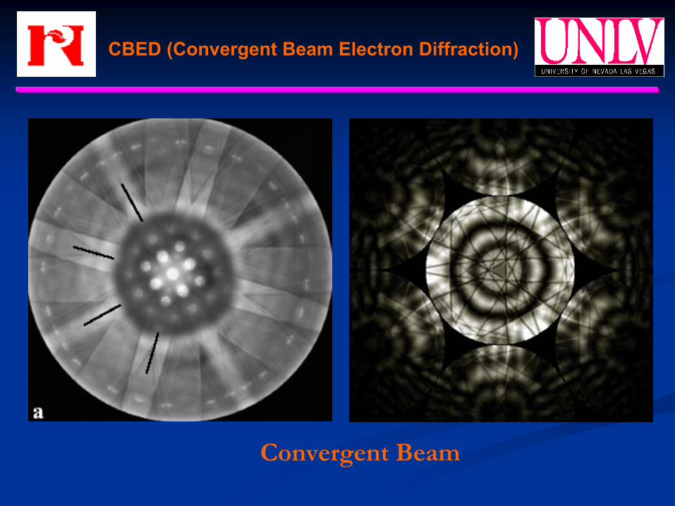
CBED (Convergent Beam Electron Diffraction)
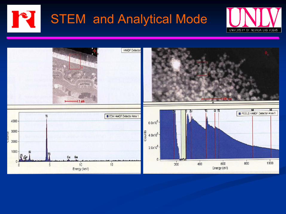
STEM and Analytical Mode
In-situ TEM
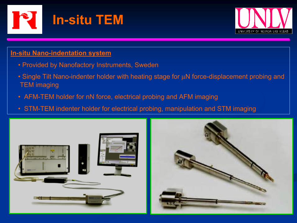
In-situ Nano-indentation system
• Provided by Nanofactory Instruments, Sweden
• Single Tilt Nano-indenter holder with heating stage for µN force-displacement probing and TEM imaging
• AFM-TEM holder for nN force, electrical probing and AFM imaging
• STM-TEM indenter holder for electrical probing, manipulation and STM imaging
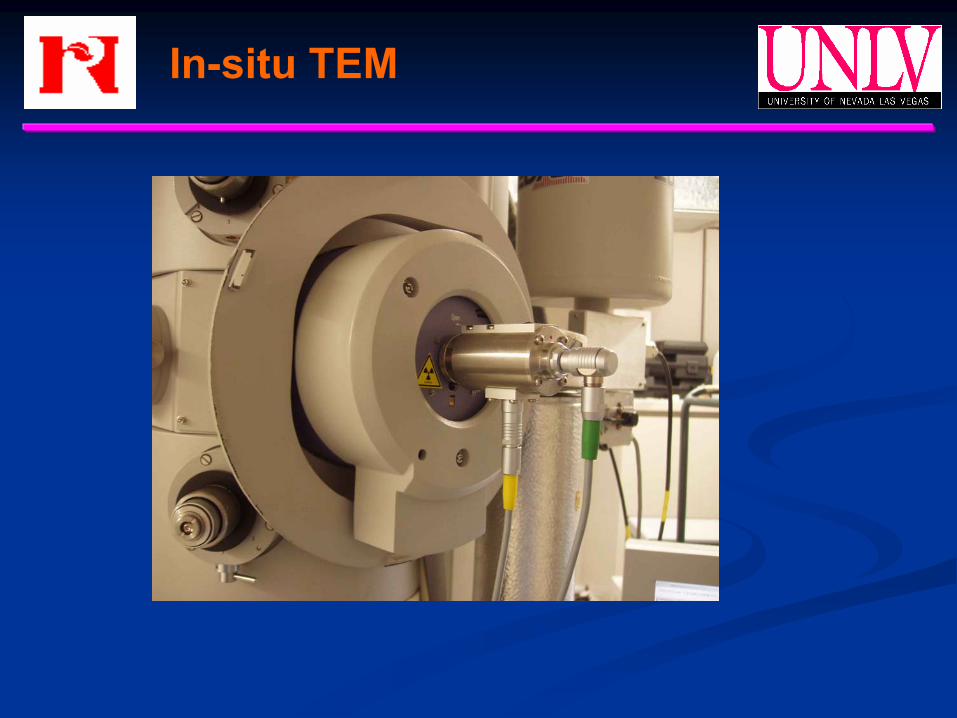
In-situ TEM
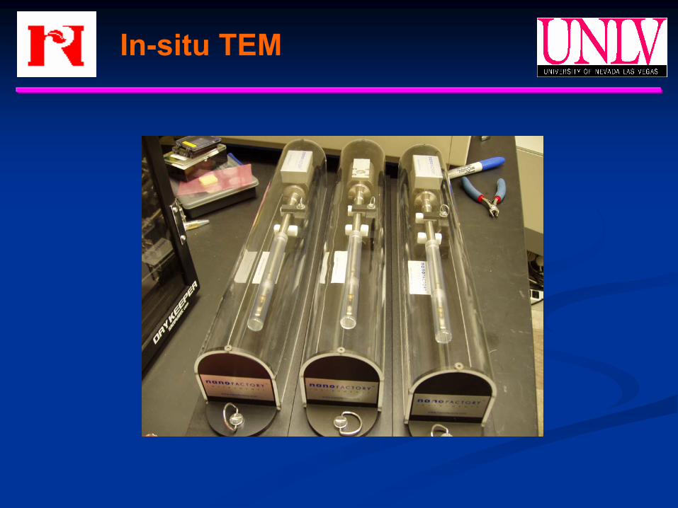
In-situ TEM
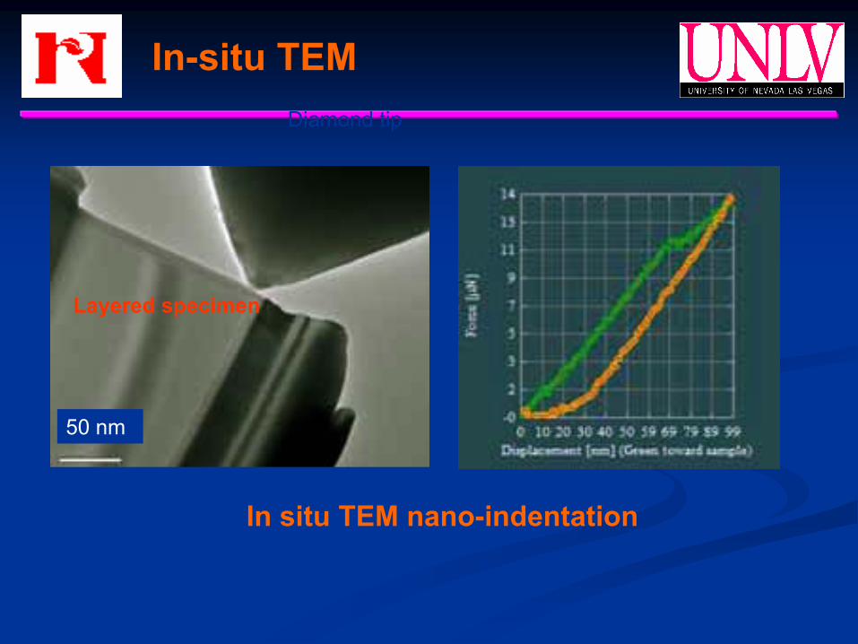
In-situ TEMDiamond tip
Layered specimen
50 nm
In situ TEM nano-indentation
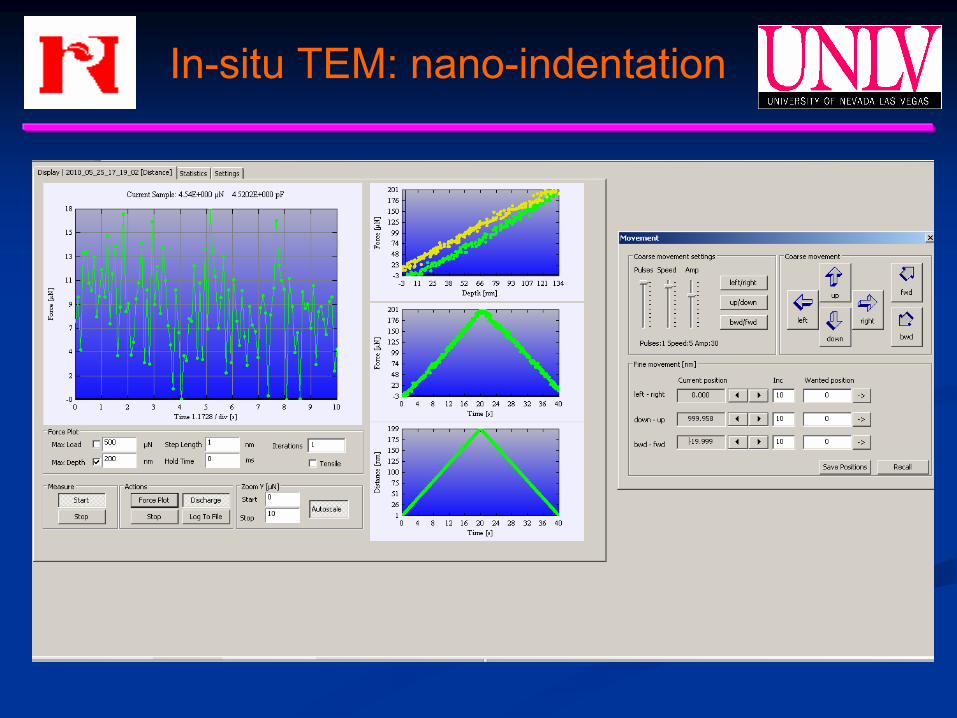
In-situ TEM: nano-indentation
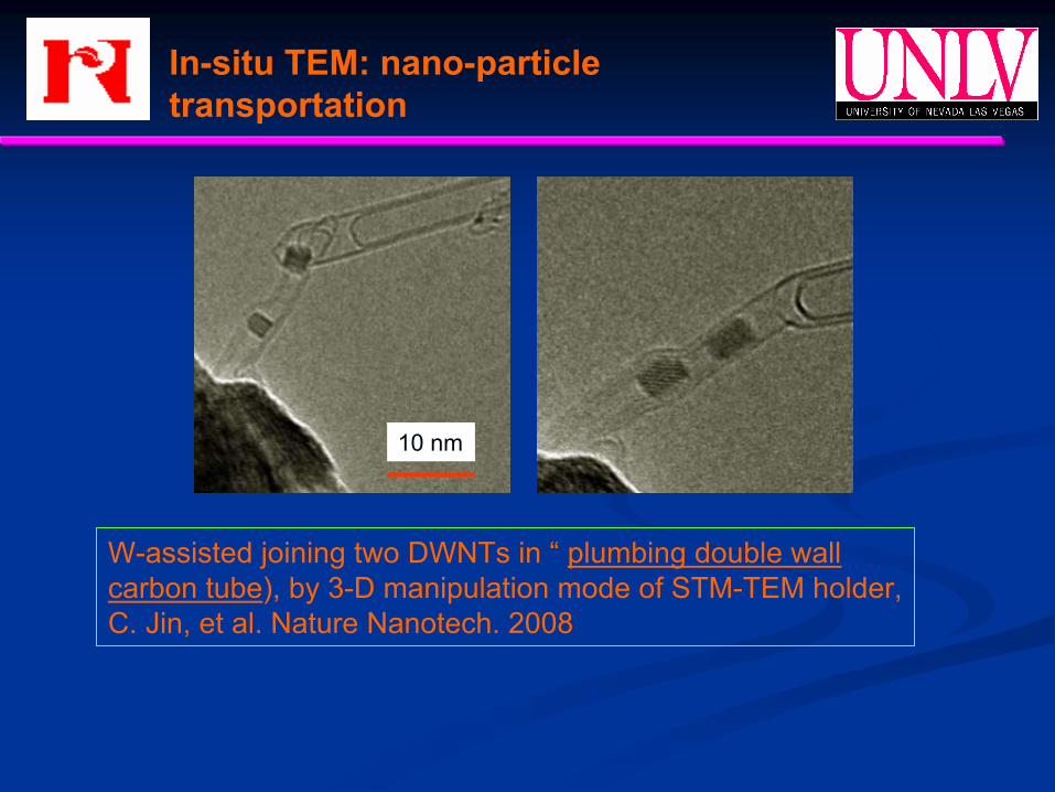
In-situ TEM: nano-particle transportation
W-assisted joining two DWNTs in “ plumbing double wall carbon tube), by 3-D manipulation mode of STM-TEM holder, C. Jin, et al. Nature Nanotech. 2008
10 nm
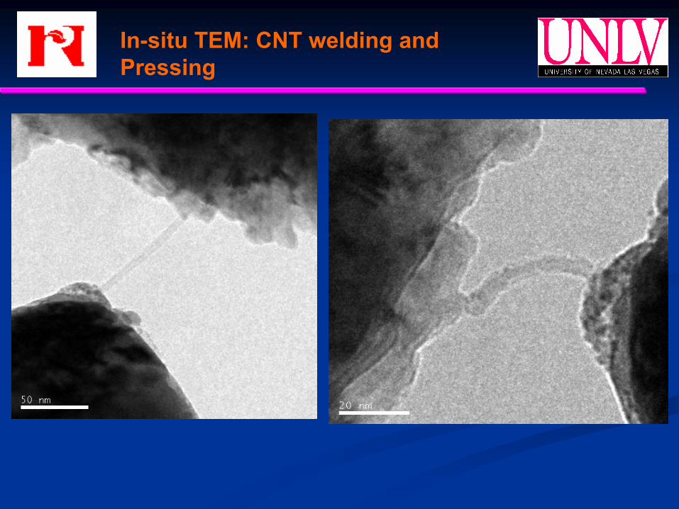
In-situ TEM: CNT welding and Pressing
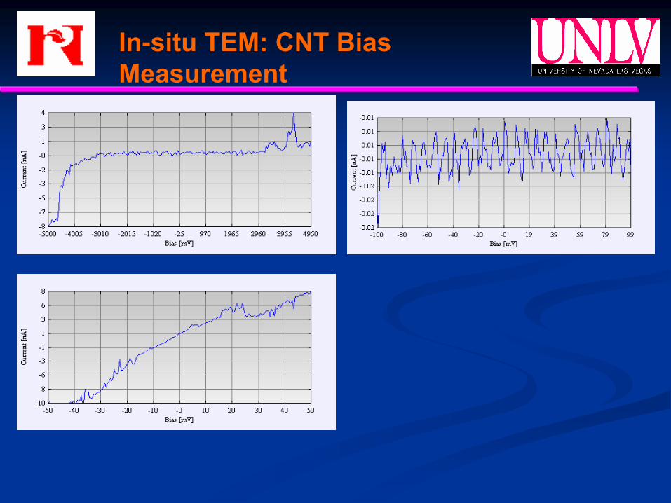
In-situ TEM: CNT Bias Measurement
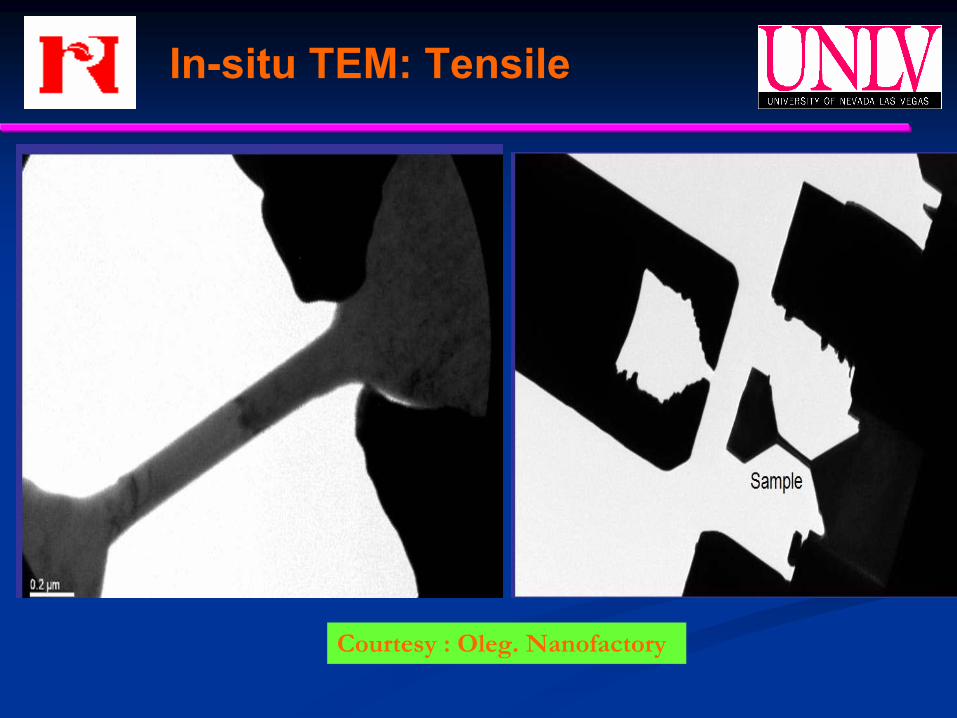
In-situ TEM: Tensile
Courtesy : Oleg. Nanofactory

Questions?