1. Transmission Electron Microscopy What is TEM?ahrenkiel.sdsmt.edu/courses/Fall2017/NANO703/... ·...
12
1 Intrumentation for Characterization of Nanomaterials (v11) 1. Transmission Electron Microscopy What is TEM? TEM can stand for either transmission electron microscope (an instrument) or transmission electron microscopy (a technique). We will use both meanings in this course. First of all, why would we choose to use electrons instead of light to image nanomaterials? Electrons require high-vacuum conditions to propagate freely, and cannot be readily focused by our eyes. Visible light can travel trough air, as well as many transparent liquids and solids, and can be easily imaged by human eyes. What are electrons? We most often think of electrons as negatively charged, fundamental particles. They move quite freely inside conductors; that motion is the basis for all of our electrical power and electronic devices. The are very light, but not massless. But all particles also have a wave aspect, which implies a wavelength and frequency. Light can be thought of as electromagnetic waves, which have a wavelength and frequency, and which, when in a vacuum, propagate at the speed of light, not surprisingly. But light may be equivalently described as massless particles: photons. 1) Shorter wavelength: The wavelengths of both electrons and photons depend on their energy, but, since electrons have mass, while photons do not have mass, the wavelength of an electron is always less than that of a photon with the same energy. We will see that the imaging resolution of a microscope is highly dependent on the wavelength of the illuminating radiation (electrons or photons), due to diffraction effects, with shorter wavelengths resulting in higher resolving power (resolution of smaller features). In a vacuum, the wavelengths of both electrons and photons decrease with increasing energy. With electrons, we can achieve much higher energies, and a broader range of energies, without significantly altering our imaging system. Visible light only spans wavelengths from roughly 400-700 nm, and though nearly perfect refracting or reflecting lenses are available in this range, the same designs are not effective for much shorter wavelengths. These shorter E-M light waves, such as X-rays, having wavelengths less than 10 nm, require specialized lenses, which may use diffraction to focus, and the quality of these has greatly improved in recent decades. But X-ray microscopes require high-brightness sources, such as synchrotrons, which are much less compact than electron microscope, and may be best suited to biological imaging, due to the challenges in preserving living tissue in the vacuum of an electron microscope column. The quality of lenses must also be considered, and electron lenses cannot be made with nearly the perfection of visible-light lenses. The Rayleigh criterion is often uses to estimate the resolving power of a lens 2sin where is the smallest resolvable feature size, is the wavelength and is the semi-angle of collection by the lens. Due to aberrations in electron lenses (which we will discuss), TEMs are generally limited to quite small values of , but the much shorter wavelengths still merit this compromise. For example, at 200 KeV (units to be discussed later), an electron has a wavelength of only 0.0025 nm. Unfortunately, the best resolution of a TEM operated at 200 KeV is not much less than 0.10 nm, but that is still much better than the best resolution of any current optical (or even X-ray) microscope.
Transcript of 1. Transmission Electron Microscopy What is TEM?ahrenkiel.sdsmt.edu/courses/Fall2017/NANO703/... ·...
1 Intrumentation for Characterization of Nanomaterials (v11)
1. Transmission Electron Microscopy
What is TEM? TEM can stand for either transmission electron microscope (an instrument) or transmission electron microscopy (a technique). We will use both meanings in this course.
First of all, why would we choose to use electrons instead of light to image nanomaterials? Electrons require high-vacuum conditions to propagate freely, and cannot be readily focused by our eyes. Visible light can travel trough air, as well as many transparent liquids and solids, and can be easily imaged by human eyes.
What are electrons? We most often think of electrons as negatively charged, fundamental particles. They move quite freely inside conductors; that motion is the basis for all of our electrical power and electronic devices. The are very light, but not massless. But all particles also have a wave aspect, which implies a wavelength and frequency.
Light can be thought of as electromagnetic waves, which have a wavelength and frequency, and which, when in a vacuum, propagate at the speed of light, not surprisingly. But light may be equivalently described as massless particles: photons.
1) Shorter wavelength: The wavelengths of both electrons and photons depend on their energy, but, since electrons have mass, while photons do not have mass, the wavelength of an electron is always less than that of a photon with the same energy. We will see that the imaging resolution of a microscope is highly dependent on the wavelength of the illuminating radiation (electrons or photons), due to diffraction effects, with shorter wavelengths resulting in higher resolving power (resolution of smaller features). In a vacuum, the wavelengths of both electrons and photons decrease with increasing energy. With electrons, we can achieve much higher energies, and a broader range of energies, without significantly altering our imaging system. Visible light only spans wavelengths from roughly 400-700 nm, and though nearly perfect refracting or reflecting lenses are available in this range, the same designs are not effective for much shorter wavelengths. These shorter E-M light waves, such as X-rays, having wavelengths less than 10 nm, require specialized lenses, which may use diffraction to focus, and the quality of these has greatly improved in recent decades. But X-ray microscopes require high-brightness sources, such as synchrotrons, which are much less compact than electron microscope, and may be best suited to biological imaging, due to the challenges in preserving living tissue in the vacuum of an electron microscope column.
The quality of lenses must also be considered, and electron lenses cannot be made with nearly the perfection of visible-light lenses. The Rayleigh criterion is often uses to estimate the resolving power of a lens
2sin
where is the smallest resolvable feature size, is the wavelength and is the semi-angle of collection
by the lens. Due to aberrations in electron lenses (which we will discuss), TEMs are generally limited to quite small values of , but the much shorter wavelengths still merit this compromise. For example, at
200 KeV (units to be discussed later), an electron has a wavelength of only 0.0025 nm. Unfortunately, the best resolution of a TEM operated at 200 KeV is not much less than 0.10 nm, but that is still much better than the best resolution of any current optical (or even X-ray) microscope.
2 Intrumentation for Characterization of Nanomaterials (v11)
2) Control of wavelength: Wavelength depends on energy, and for electrons, the energy results from acceleration through an electrical potential (voltage). Variable electrical power supplies are relatively common (although the voltages needed for TEM are exceptionally high.) With a good voltage source, our electron energy can not only be adjusted to meet certain conditions, but can also transfer the same energy to all of the beam electrons, so the electron beam is very nearly monochromatic. For visible light, monochromatic illumination requires either a filter or grating from a broad spectrum source, which reject the unwanted energies, or a laser, which usually has a fixed wavelength.
3) Smaller probe sizes: The minimum size to which a beam can be focused by a lens to form a small probe is closely related to the resolving power of the lens. These two configurations are, in fact, related by a principle of reciprocity, with now representing the minimum probe size. In scanning electron microscopy, as well as scanning TEM, we often wish to generate one or more forms of signal by illuminating the smallest possible sample volume with a focused probe. Thus, shorter wavelengths again give the advantage to high-energy electrons over light for imaging nanomaterials.
4) Interaction with core electrons: Different types of radiation (e.g., electrons, photons, neutrons, He ions) all interact with matter in different ways, and certainly all have their advantages and disadvantages towards their use for imaging. But both electrons and X-ray photons are ionizing radiation, causing core electrons to be ejected from atoms. One outcome of ionization is X-ray fluorescence. The characteristic X-ray spectra of atoms are well known, so identification of the constituent elements is possible by detection of the X-rays when a specimen is exposed to the microscope beam, providing a method for chemically sensitive detection of most of the elements on the periodic table.
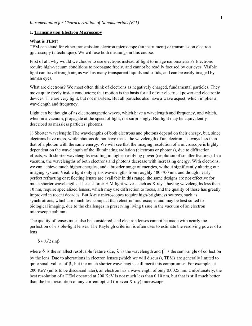
A brief history of microscopy & diffraction (I) Invention of the earliest simple optical microscope is credited to van Leeuwenhoek in the 1670s. He built a stage that allowed positioning a sample with respect to a single glass lens, similar to a magnifying glass. Shortly thereafter, Hooke built the first compound microscope, which reduces the strain on the eye for focusing. Optical microscopes developed substantially over the next two centuries, and by the late 1800s, Airy, Rayleigh, and Abbe had all developed theoretical models for optical microscopy and limitations on the best achievable resolution, which was realized to be limited by the wavelength of light. In the early 20th century, J. J. Thomson realized that electrons were charged particles. He accelerated them through an electrical potential and deflected them in a magnetic field, which allowed measurement of their charge-to-mass ratio. Von Laue and the Braggs won Nobel prizes in 1914 and 1915, respectively, for discovering X-ray diffraction and realizing that this provided both evidence of crystal structure in materials and a means to determine that structure.
3 Intrumentation for Characterization of Nanomaterials (v11)
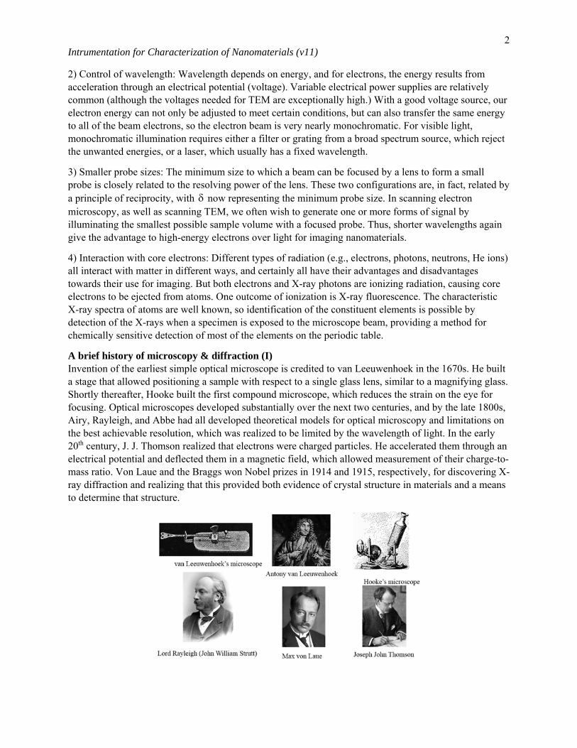
A brief history of microscopy & diffraction (II) In the 1920s, de Broglie proposed that not only light, but also electrons and all matter and energy have both a wave and a particle nature. Shortly thereafter, G. P. Thomson, and separately Davisson and Germer, observed the diffraction of electrons from crystals, which proved wave/particle duality. But, in contrast to X rays, which do not have electrical charge, electrons undergo many scattering events when interacting with crystals. Bethe developed one of the first theories of dynamical electron diffraction to explain the propagation of a high-energy electron through a crystal.
It was the charge of the electrons that inspired engineers to consider forming images with electrons. They realized that it was possible to focus the electrons with either electric or magnetic fields. Busch, Ruska, Knoll, and Rudenberg are credited with much of the early technology that emerged in the 1930s and 40s that enabled electron microscopy. It was then that electron microscopy and its application to materials began to flourish. Scientists such as Cowely, Howie, Spence, Tanaka, Hirsch, and Gjønnes are credited with contributions in the following decades towards the development of electron diffraction and imaging techniques that form the basis for modern transmission electron microscopy.
Electron microscopy facilities There are a number of high-end user facilities throughout the U.S. that provide access to cutting-edge or highly specialized, as well as routine, electron microscopy analysis. Some notable examples are listed below:
National Laboratories:
Electron Microscopy Center (www.anl.gov/cnm/group/electron-microscopy-center) at Argonne National Laboratory, now part of the Center for Nanoscale Materials.
Electron Microscopy Facility (www.bnl.gov/cfn/facilities/microscopy.php) in the Center for Functional Nanomaterials at Brookhaven National Laboratory
National Center for Electron Microscopy (foundry.lbl.gov/facilities/ncem/), within the Molecular Foundry at Lawrence Berkeley National Laboratory
Universities:
John M. Cowley Center for High-Resolution Electron Microscopy (asu.corefacilities.org/service_center/show_external/3195/john-m-cowley-center-for-high-resolution-electron-microscopy-chrem) at Arizona State University
Center for Advanced Materials and Nanotechnology (www.lehigh.edu/nano/emf_facility.html) at Lehigh University
Boulder Laboratory for 3-D Electron Microscopy of Cells (bio3d.colorado.edu/) at University of Colorado, Boulder

4 Intrumentation for Characterization of Nanomaterials (v11)
Commercial TEM models and manufacturers Four companies presently make commercially available TEMs and S/TEMs: Hitachi (hitachi-hta.com), JEOL (http://www.jeol.com/) FEI (www.fei.com) and Zeiss (no?). RCA, Seimens, and Philips were all early providers of commercial TEMs. Nion (www.nion.com/index.html) manufactures dedicated STEMs.
Evolution of commercial TEMs Some early TEM models used permanent magnets, rather than electromagnets, for focusing, or were were inverted with respect to current, top-down models, having the electron source below the viewing screen. Electon-sensitive film was used for several decades as the primary means of recording images. Modern TEMs have digital control and digital cameras, most often using CCD or CMOS sensors, with incident electrons converted to light on a phosphor, then back into electrons for readout. The increase to accelerating potentials exceeding 100 KV has required higher vacuums, both for generating the beam and preserving the specimen.
Imaging and presentation software Digital image capture and presentation requires software to control and readout the camera, archive the images, and transform them for presentation. Most image recording software is camera specific and proprietary, but some very useful software for these purposes is now free for manipulating saved images in common formats (e.g., TIFF). Digital Micrograph(Gatan, www.gatan.com/products/tem-analysis/gatan-microscopy-suite-software) and ImageJ (NIH, imagej.nih.gov/ij/) both allow image capture from various cameras. Digital Micrograph is available in a free offline version, with a powerful scripting language for image-related computations. ImageJ is free, and plug-ins are available for a range of
5 Intrumentation for Characterization of Nanomaterials (v11)
common tasks. Photoshop, and its freeware counterpart, GIMP, both provide for image processing, with some features for annotation. Illustrator also has a freeware counterpart, Inkscape, and both provide a range of tools to annotate figures that can be exported into final documents or presentations.
Higher voltage/energy It seems reasonable, upon first thought, that shorter wavelengths allow for higher resolution images. We will see later that the diffraction-limited resolvable feature size is smaller, and lens aberrations are less severe, when higher energy electrons are used. But is it always better to have a higher voltage/higher energy electron microscope? We can penetrate through a thicker specimen with a higher energy beam. But, on the other hand, if we are trying to image the surface of a thick specimen, we may not want the beam to penetrate below the sample surface, because this will generate a larger interaction volume and ultimately reduce the image resolution, so a lower voltage may be better. With more energy per electron, images will be more intense, but then there is less image contrast. Diffraction patterns scale as inverse wavelength, so with a higher energy, there will be more diffraction features present, but those features will be more closely spaced, making it more difficult to isolate particular reflections, as is needed for dark-field imaging. High-energy electrons cause less charging of thin specimens, which can improve imaging, but can also alter crystal structure, and and particularly affect biological samples. Lastly, higher energy requires a larger, more expensive and complex voltage source, a bigger/taller beam column, higher level of vacuum, and greater shielding from unwanted radiation.
The distinction is sometimes made between high-voltage (1-3 MV) and intermediate voltage (<1 MV) TEMs. The most popular for laboratory use have maximum voltages of 200-400 KV. Higher resolutions require more ideal laboratory environmental conditions, such as vibration isolation, magnetic shielding, and specialized air control. The biggest resolution improvements in recent years have come from new types of aberration correctors, which replace conventional lenses with ideal lenses. Resolution improvements from continuing to higher energies are only incremental, and usually a particular need must exist to justify the higher-voltage instruments.
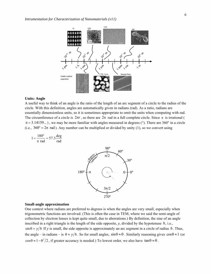
Units: Length Microscopes may be useful in imaging features as large as ants or insects, on the scale of 1 mm (1 mm=10-3 m). A common reference is the width of a human hair, roughly 50-100 um (1 m=10-6 m). Topographic features on a compact disk are on a scale of a few m, a few times larger than the wavelength of visible light. Viruses, such as influenza, are sub-micron, typically 100-200 nm (1 nm=10-9 m). Nanoparticles and quantum dots are usually considered to be aggregates of matter smaller than about 100 nm. Carbon nanotubes are some of the most widely recognized nanomaterials, perhaps spurring much of the modern interest in nanoscience. Nanotubes range in diameter from slightly bigger than 1 nm to around 10 nm. The interplanar spacings in crystalline materials are usually smaller than 1 nm. A common unit of measure for crystal lattice spacings is angstroms (1 Å=10-10 m). The resolution of so-called “dumbbells” - individual atomic columns in crystal Si, having sub-Å spacing, is considered one of the showpieces of the most recent generation of high-resolution scanning TEMs, which use new detector geometries and aberration correctors to push the conventional resolution limitations.
6 Intrumentation for Characterization of Nanomaterials (v11)
Units: Angle A useful way to think of an angle is the ratio of the length of an arc segment of a circle to the radius of the circle. With this definition, angles are automatically given in radians (rad). As a ratio, radians are essentially dimensionless units, so it is sometimes appropriate to omit the units when computing with rad. The circumference of a circle is 2 r , so there are 2 rad in a full complete circle. Since is irrational (
3.14159... ) , we may be more familiar with angles measured in degrees (°). There are 360° in a circle (i.e., 360 2 rad ). Any number can be multiplied or divided by unity (1), so we convert using
180 deg1 57.3
rad rad
Small-angle approximation One context where radians are preferred to degrees is when the angles are very small, especially when trigonometric functions are involved. (This is often the case in TEM, where we said the semi-angle of collection by electron lenses is kept quite small, due to aberrations.) By definition, the sine of an angle inscribed in a right triangle is the length of the side opposite, y, divided by the hypotenuse h , i.e., sin y h If y is small, the side opposite is approximately an arc segment in a circle of radius h . Thus,
the angle – in radians – is y h . So for small angles, sin . Similarly reasoning gives cos 1 (or 2cos 1 2 , if greater accuracy is needed.) To lowest order, we also have tan .

7 Intrumentation for Characterization of Nanomaterials (v11)
So what is a “typical” small angle? The distinction is a bit arbitrary, but a common threshold is 10 mrad (1 mrad =10-3 rad). Don’t believe me? Enter 0.01 into your calculator. Be sure you are in rad mode, and press “sin”. The result is sin(0.010 rad) 0.0099998... , so the approximation is quite adequate up to a few
tens of mrad. For reference, you may know that the angle subtended by both the sun and moon, when viewed from the earth’s surface is about 0.50 8.7 rad ; slightly less than 10 mrad, so small by our standards.
Physical constants A few physical constants are needed to quantify electron diffraction pattern and image formation. The fundamental charge on an electron is denoted e , the speed of light in a vacuum is c , Planck’s constant – of purely quantum-mechanical origin – is h , and the electron rest mass is 0m .
quantity symbol value elementary charge e 191.60 10 Ce speed of light c 83.00 10 m sc Planck’s constant h 346.63 10 J sh electron rest mass 0m 31
0 9.11 10 kgm
More physical units We have already assumed some knowledge of physical units. In the SI system, force is given in newtons (N), energy is given in joules (J), electric potential (voltage) in volts (V), electric current in amperes (A). But when discussing the energy of electrons or other charged particles, there is another important unit: the electron volt (eV). An electron at an electrical potential of 1 V has a potential energy of 1 eV.
unit symbol definition newton N 21 N 1 kg m s joule J 1 J 1 N m volt V 1 V 1 J C ampere A 1 A 1 C s electron volt eV 191 eV 1.602 10 J
There some useful shortcuts that crop up. For example, we often encounter the product 1240 eV nm 1.24 KeV nmh c . If we apply Einstein’s energy-mass relationship to electrons, we
will find 20 511 KeVm c .
8 Intrumentation for Characterization of Nanomaterials (v11)
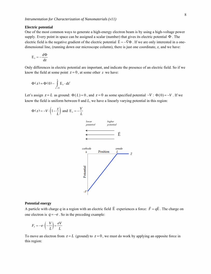
Electric potential One of the most common ways to generate a high-energy electron beam is by using a high-voltage power supply. Every point in space can be assigned a scalar (number) that gives its electric potential . The
electric field is the negative gradient of the electric potential E
. If we are only interested in a one-dimensional line, (running down our microscope column), there is just one coordinate, z, and we have:
E zd
dz
Only differences in electric potential are important, and indicate the presence of an electric field. So if we know the field at some point 0z , at some other z we have:
0
0 Ez
z
z
z dz
Let’s assign z L as ground: 0L , and 0z as some specified potential V : 0 V . If we
know the field is uniform between 0 and L, we have a linearly varying potential in this region:
1z
z VL
and E zV
L
Potential energy
A particle with charge q in a region with an electric field Ε
experiences a force: EF q
. The charge on
one electron is q e . So in the preceding example:
zV eV
F eL L
To move an electron from z L (ground) to 0z , we must do work by applying an opposite force in this region:
9 Intrumentation for Characterization of Nanomaterials (v11)
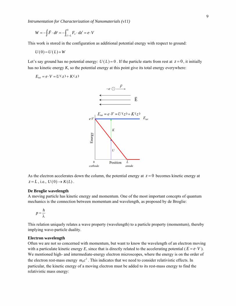
0
zz L
W F dr F dz e V
This work is stored in the configuration as additional potential energy with respect to ground:
0U U L W
Let’s say ground has no potential energy: 0U L . If the particle starts from rest at 0z , it initially
has no kinetic energy K, so the potential energy at this point give its total energy everywhere:
totE e V U z K z
As the electron accelerates down the column, the potential energy at 0z becomes kinetic energy atz L , i.e., (0 )U K L .
De Broglie wavelength A moving particle has kinetic energy and momentum. One of the most important concepts of quantum mechanics is the connection between momentum and wavelength, as proposed by de Broglie:
hp
This relation uniquely relates a wave property (wavelength) to a particle property (momentum), thereby implying wave-particle duality.
Electron wavelength Often we are not so concerned with momentum, but want to know the wavelength of an electron moving with a particulate kinetic energy E, since that is directly related to the accelerating potential ( E e V ). We mentioned high- and intermediate-energy electron microscopes, where the energy is on the order of
the electron rest-mass energy 20m c . This indicates that we need to consider relativistic effects. In
particular, the kinetic energy of a moving electron must be added to its rest-mass energy to find the relativistic mass energy:
10 Intrumentation for Characterization of Nanomaterials (v11)
2 20mc E m c
Relativity also reveals that
0m m
where is the Lorentz factor
21 1 v c
Here v is the speed. We can relate speed to momentum using p mv to establish a well-known relation
in relatively:
2 2 22 20mc m c pc
Now we use the de Broglie relation and substitute:
2 22 20 0
h hc hc
p pc E m c m c
After a little algebra:
202
hc
E E m c
WE WILL USE THIS FORM THROUGHOUT THIS CLASS!
Non-relativistic electron wavelength
At much lower energies ( 202E m c ), we can approximate 2 2
0 02 2E m c m c , so
200 22
nrhc h
m EE m c
DO NOT USE THIS FORM IN THIS CLASS!
Comparison The non-relativistic form will overestimate the wavelength at high energies. Notice that the two are related by:
20
12
nr
Em c
so nr
Oddly, we sometimes do use the non-relativistic form, but substitute a corrected energy that gives the right wavelength.
2 nr
h
mE
11 Intrumentation for Characterization of Nanomaterials (v11)
This non-relativistic energy is defined as:
0
2nr
m mE E
m
We know that 0m m , so nrE E .
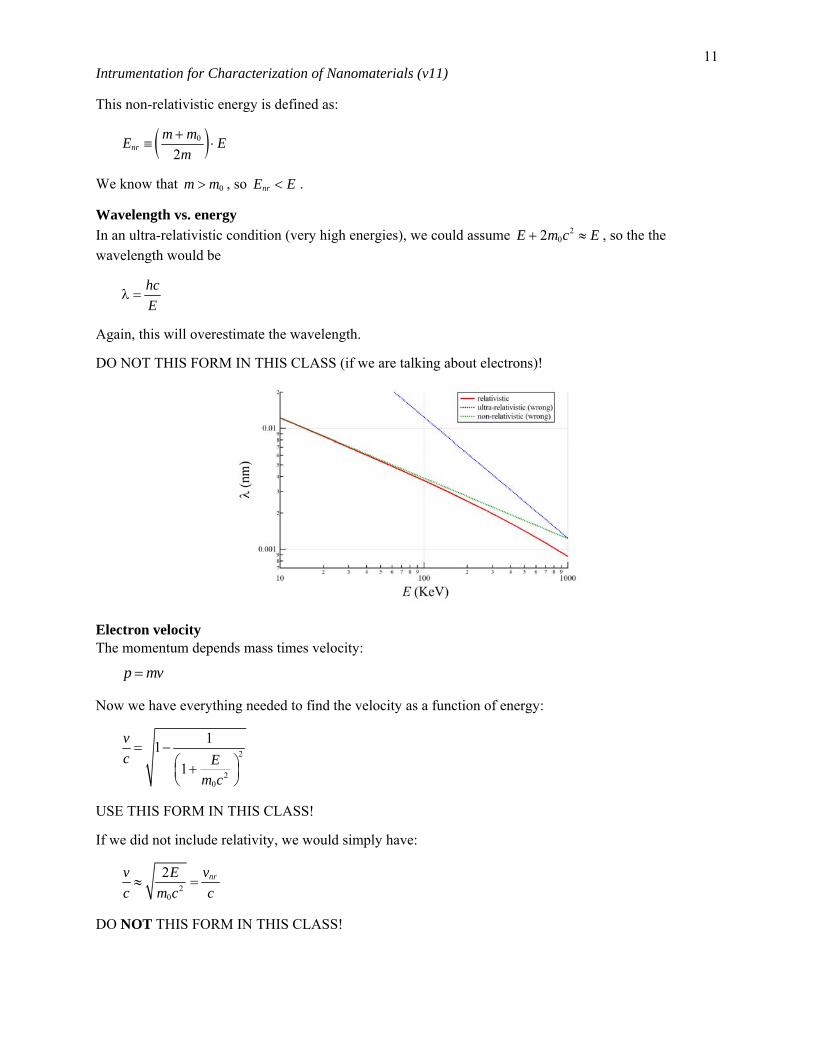
Wavelength vs. energy
In an ultra-relativistic condition (very high energies), we could assume 202E m c E , so the the
wavelength would be
hc
E
Again, this will overestimate the wavelength.
DO NOT THIS FORM IN THIS CLASS (if we are talking about electrons)!
Electron velocity The momentum depends mass times velocity:
p mv
Now we have everything needed to find the velocity as a function of energy:
2
20
11
1
v
c E
m c
USE THIS FORM IN THIS CLASS!
If we did not include relativity, we would simply have:
20
2 nrv E v
c m c c
DO NOT THIS FORM IN THIS CLASS!
12 Intrumentation for Characterization of Nanomaterials (v11)
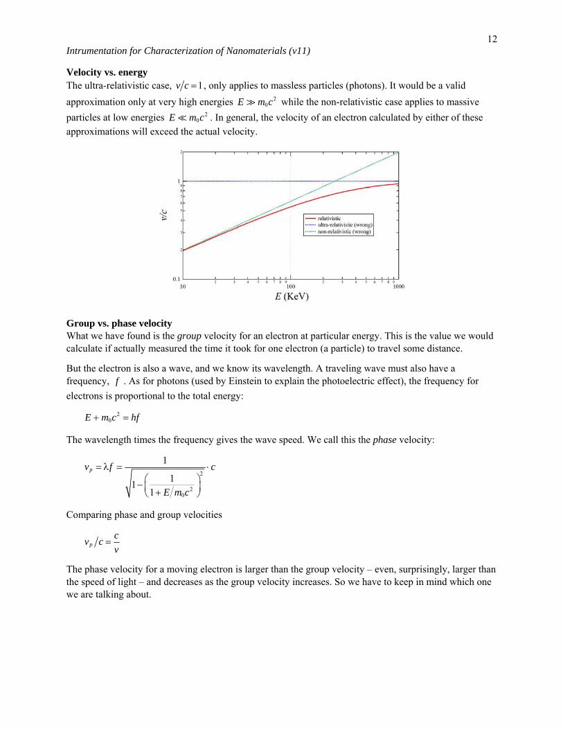
Velocity vs. energy The ultra-relativistic case, 1v c , only applies to massless particles (photons). It would be a valid
approximation only at very high energies 20E m c while the non-relativistic case applies to massive
particles at low energies 20E m c . In general, the velocity of an electron calculated by either of these
approximations will exceed the actual velocity.
Group vs. phase velocity What we have found is the group velocity for an electron at particular energy. This is the value we would calculate if actually measured the time it took for one electron (a particle) to travel some distance.
But the electron is also a wave, and we know its wavelength. A traveling wave must also have a frequency, f . As for photons (used by Einstein to explain the photoelectric effect), the frequency for
electrons is proportional to the total energy:
20E m c hf
The wavelength times the frequency gives the wave speed. We call this the phase velocity:
2
20
1
11
1
pv f c
E m c
Comparing phase and group velocities
pc
v cv
The phase velocity for a moving electron is larger than the group velocity – even, surprisingly, larger than the speed of light – and decreases as the group velocity increases. So we have to keep in mind which one we are talking about.