Transmission Electron Microscopy -TEM- - Dipartimento di ...rocca/Didattica/Laboratorio/s in... ·...
65
Transmission Electron Microscopy -TEM- The first electron microscope was built 1932 by the German physicist Ernst Ruska, who was awarded the Nobel Prize in 1986 for its invention. He knew that electrons possess a wave aspect, so he believed he could treat them in a fashion similar to light waves. Ruska was also aware that magnetic fields could affect electron trajectories, possibly focusing them as optical lenses do to light. After confirming these principles through research, he set out to design the electron microscope. Ruska had deduced that an electron microscope would be much more powerful than an ordinary optical microscope since electron waves were shorter than ordinary light waves and electrons would allow for greater magnification and thus to visualize much smaller structures. The first crude electron microscope was capable of magnifying objects 400 times. The first practical electron microscope was built by in 1938 and had 10 nm resolution. Although modern electron microscopes can magnify an object 2 million times, they are still based upon Ruska's prototype and his correlation between wavelength and magnification. The electron microscope is now an integral part of many laboratories. Researchers use it to examine biological materials (such as microorganisms and cells), a variety of large molecules, medical biopsy samples, metals and crystalline structures, and the characteristics of various surfaces.
Transcript of Transmission Electron Microscopy -TEM- - Dipartimento di ...rocca/Didattica/Laboratorio/s in... ·...
Transmission Electron Microscopy
-TEM-
The first electron microscope was built 1932 by the German physicist Ernst Ruska, who
was awarded the Nobel Prize in 1986 for its invention. He knew that electrons possess a
wave aspect, so he believed he could treat them in a fashion similar to light waves. Ruska
was also aware that magnetic fields could affect electron trajectories, possibly focusing
them as optical lenses do to light. After confirming these principles through research, he set
out to design the electron microscope. Ruska had deduced that an electron microscope
would be much more powerful than an ordinary optical microscope since electron waves
were shorter than ordinary light waves and electrons would allow for greater magnification
and thus to visualize much smaller structures. The first crude electron microscope was
capable of magnifying objects 400 times. The first practical electron microscope was built
by in 1938 and had 10 nm resolution. Although modern electron microscopes can magnify
an object 2 million times, they are still based upon Ruska's prototype and his correlation
between wavelength and magnification. The electron microscope is now an integral part of
many laboratories. Researchers use it to examine biological materials (such as
microorganisms and cells), a variety of large molecules, medical biopsy samples, metals
and crystalline structures, and the characteristics of various surfaces.
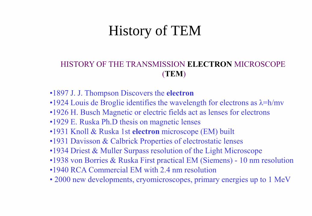
HISTORY OF THE TRANSMISSION ELECTRON MICROSCOPE
(TEM)
•1897 J. J. Thompson Discovers the electron
•1924 Louis de Broglie identifies the wavelength for electrons as λ=h/mv
•1926 H. Busch Magnetic or electric fields act as lenses for electrons
•1929 E. Ruska Ph.D thesis on magnetic lenses
•1931 Knoll & Ruska 1st electron microscope (EM) built
•1931 Davisson & Calbrick Properties of electrostatic lenses
•1934 Driest & Muller Surpass resolution of the Light Microscope
•1938 von Borries & Ruska First practical EM (Siemens) - 10 nm resolution
•1940 RCA Commercial EM with 2.4 nm resolution
• 2000 new developments, cryomicroscopes, primary energies up to 1 MeV
History of TEM
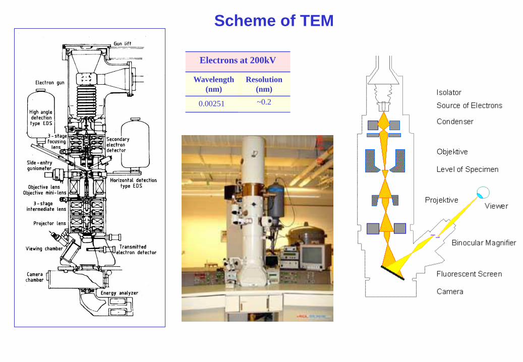
Scheme of TEM
0.00251
Resolution
(nm)
Wavelength
(nm)
Electrons at 200kV
~0.2
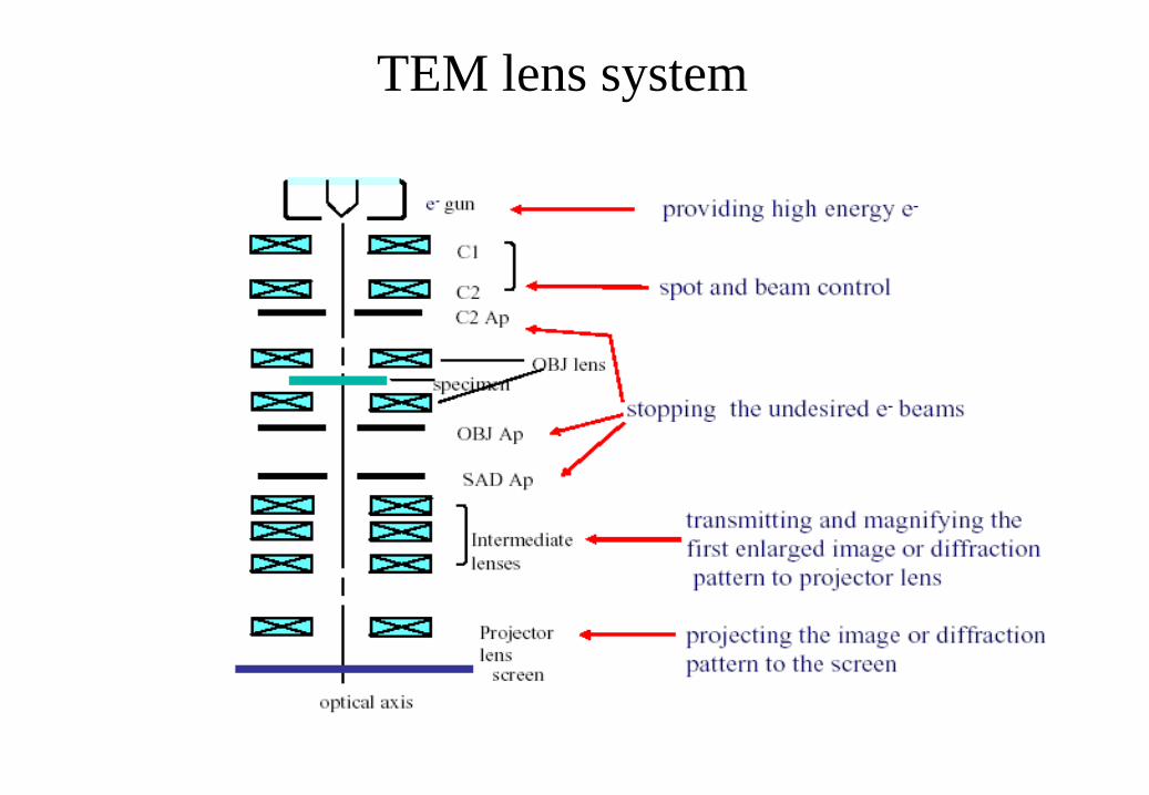
TEM lens system
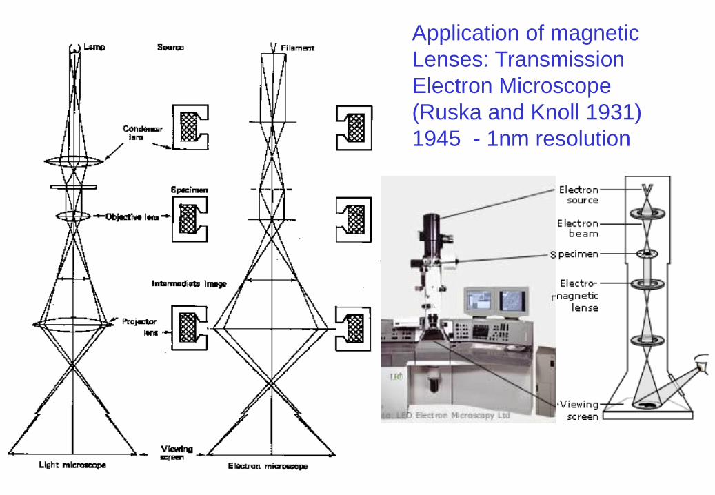
Application of magnetic
Lenses: Transmission
Electron Microscope
(Ruska and Knoll 1931)
1945 - 1nm resolution
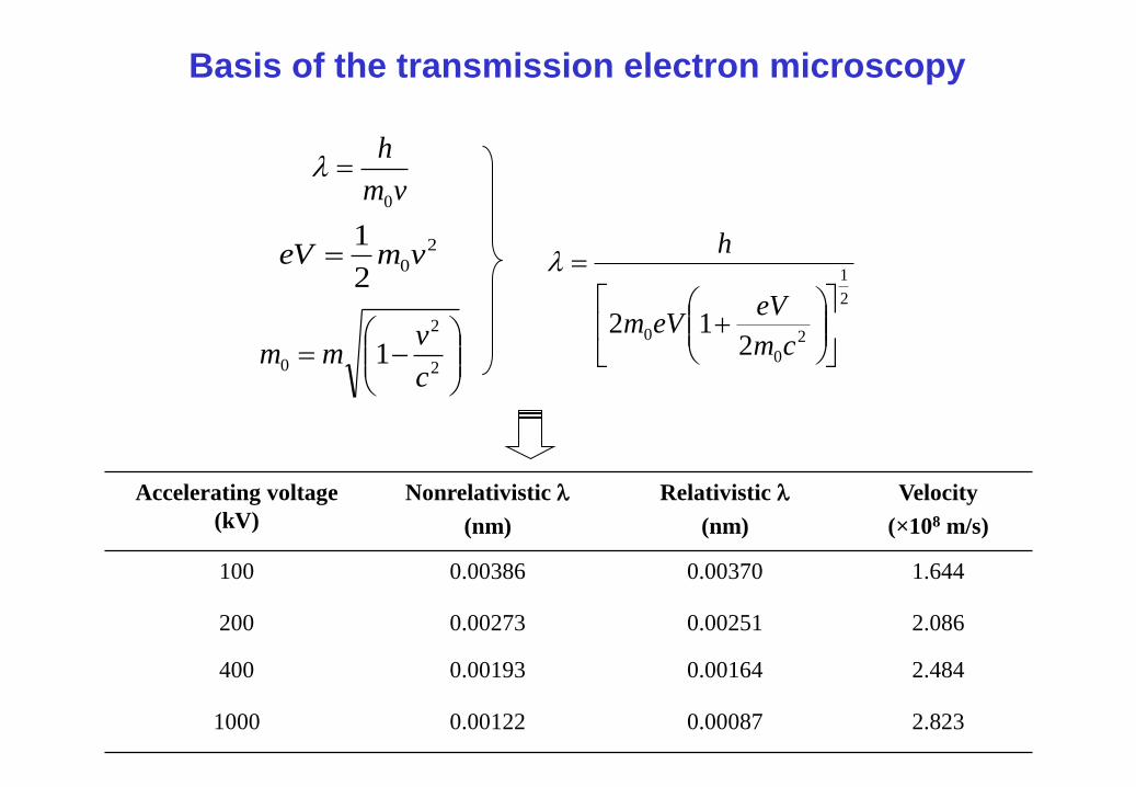
Accelerating voltage
(kV)
Nonrelativistic l
(nm)
Relativistic l
(nm)
Velocity
(×108 m/s)
100 0.00386 0.00370 1.644
200 0.00273 0.00251 2.086
400 0.00193 0.00164 2.484
1000 0.00122 0.00087 2.823
vm
h
0
l
2
02
1vmeV
2
1
2
0
02
12
cm
eVeVm
hl
2
2
0 1c
vmm
Basis of the transmission electron microscopy
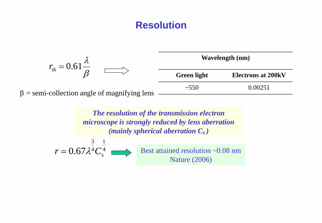
l61.0thr
0.00251 ~550
Electrons at 200kV Green light
Wavelength (nm)
4
1
4
3
67.0 sCr l
Resolution
Best attained resolution ~0.08 nm
Nature (2006)
The resolution of the transmission electron
microscope is strongly reduced by lens aberration
(mainly spherical aberration Cs )
= semi-collection angle of magnifying lens
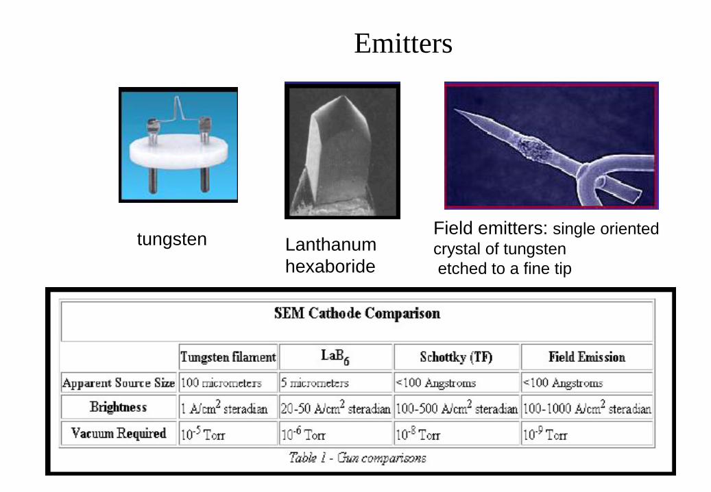
Emitters
tungsten Lanthanum
hexaboride
Field emitters: single oriented
crystal of tungsten
etched to a fine tip
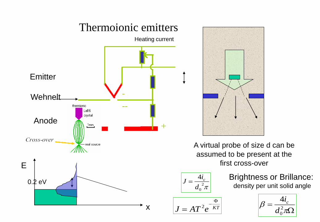
Thermoionic emitters
KTeATJ
2
A virtual probe of size d can be assumed to be present at the
first cross-over
J
2
0
4
d
iJ c
Brightness or Brillance: density per unit solid angle
Heating current
E
x
Emitter
Wehnelt
Anode
0.2 eV
2
0
4
d
ic
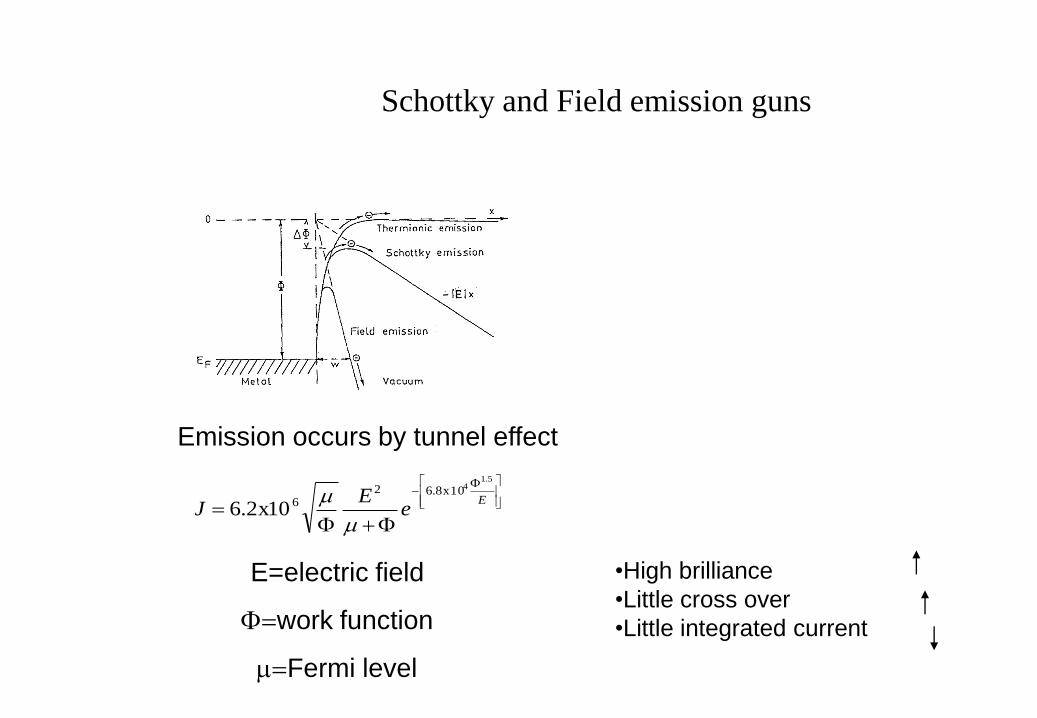
Schottky and Field emission guns
Ee
EJ
5.14x108.62
6x102.6
Emission occurs by tunnel effect
E=electric field
work function
Fermi level
•High brilliance
•Little cross over
•Little integrated current
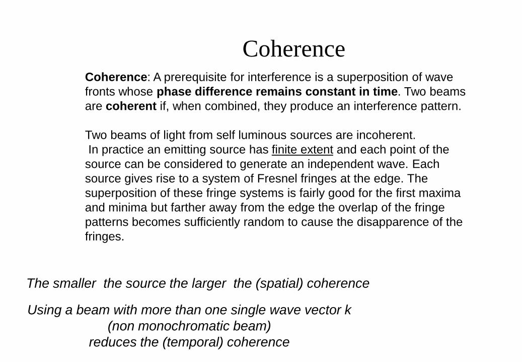
Coherence Coherence: A prerequisite for interference is a superposition of wave
fronts whose phase difference remains constant in time. Two beams
are coherent if, when combined, they produce an interference pattern.
Two beams of light from self luminous sources are incoherent.
In practice an emitting source has finite extent and each point of the
source can be considered to generate an independent wave. Each
source gives rise to a system of Fresnel fringes at the edge. The
superposition of these fringe systems is fairly good for the first maxima
and minima but farther away from the edge the overlap of the fringe
patterns becomes sufficiently random to cause the disapparence of the
fringes.
The smaller the source the larger the (spatial) coherence
Using a beam with more than one single wave vector k
(non monochromatic beam)
reduces the (temporal) coherence
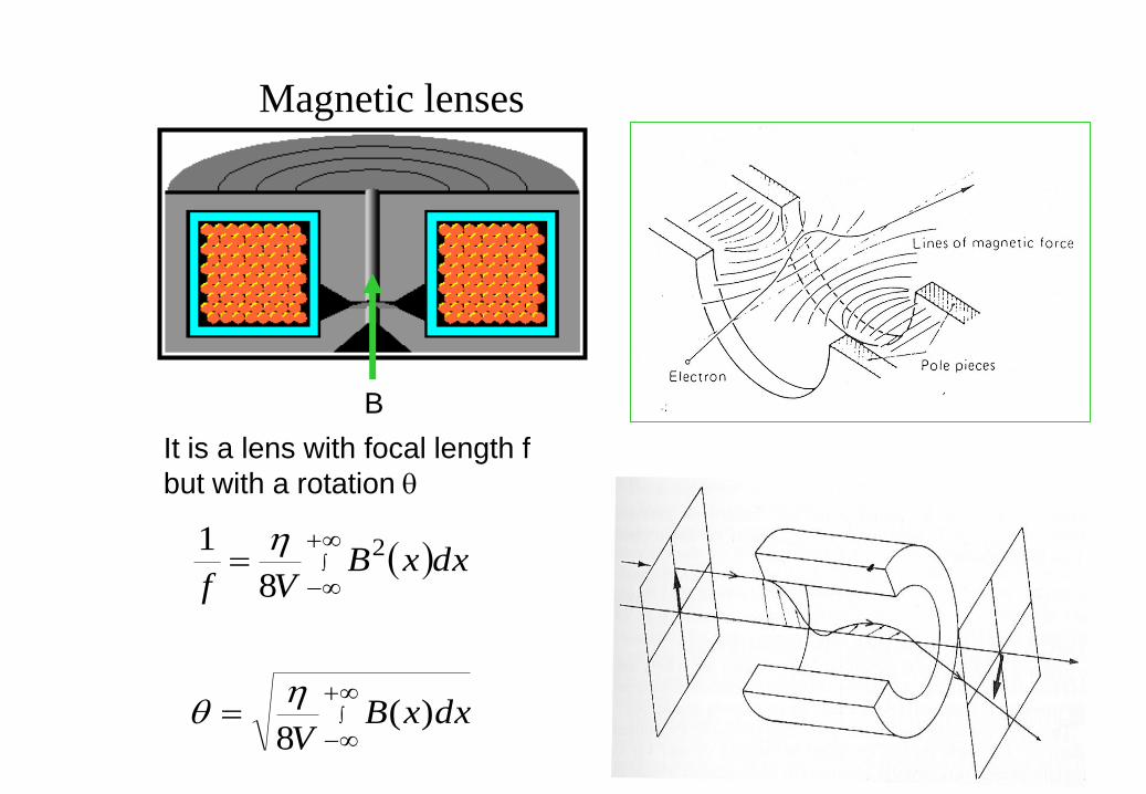
B
Magnetic lenses
dxxBV
dxxBVf
)(8
8
1 2
It is a lens with focal length f
but with a rotation
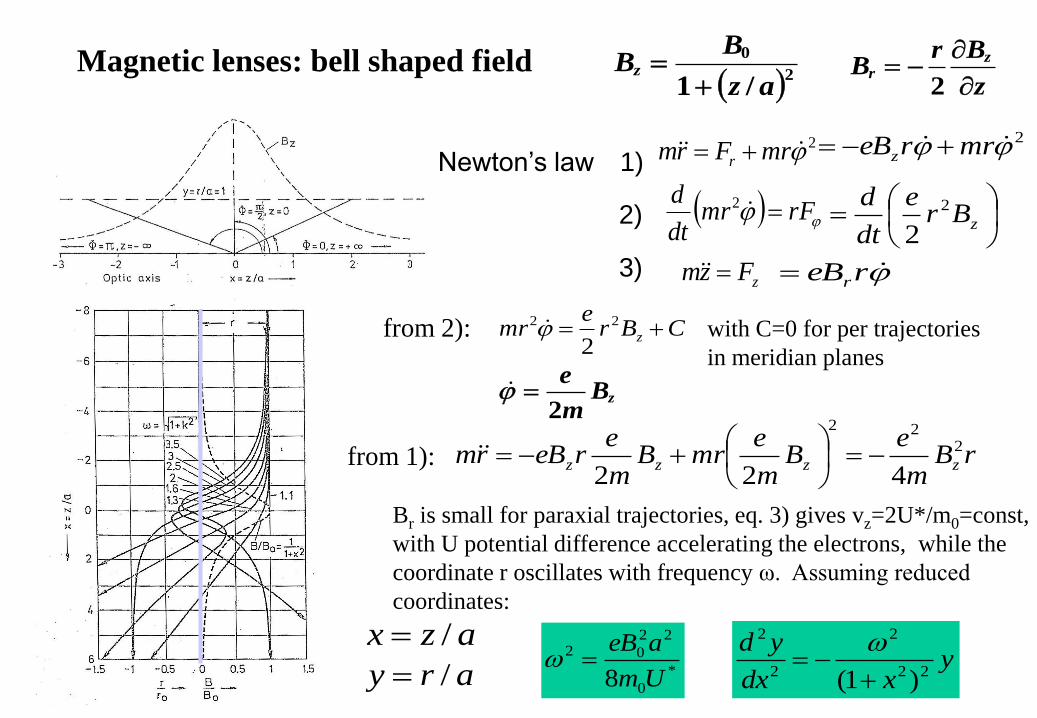
Magnetic lenses: bell shaped field 2
0
/1 az
BBz
z
BrB
zr
2
Newton’s law
3)
2 mrFrm r
rFmrdt
d2
zFzm
2 mrreBz
zBr
e
dt
d 2
2
reBr
1)
2)
CBre
mr z 22
2
zBm
e
2
Br is small for paraxial trajectories, eq. 3) gives vz=2U*/m0=const,
with U potential difference accelerating the electrons, while the
coordinate r oscillates with frequency ω. Assuming reduced
coordinates:
rBm
eB
m
emrB
m
ereBrm zzzz
222
422
ary /
azx /*
0
22
02
8 Um
aeB y
xdx
yd22
2
2
2
)1(
from 2):
from 1):
with C=0 for per trajectories
in meridian planes
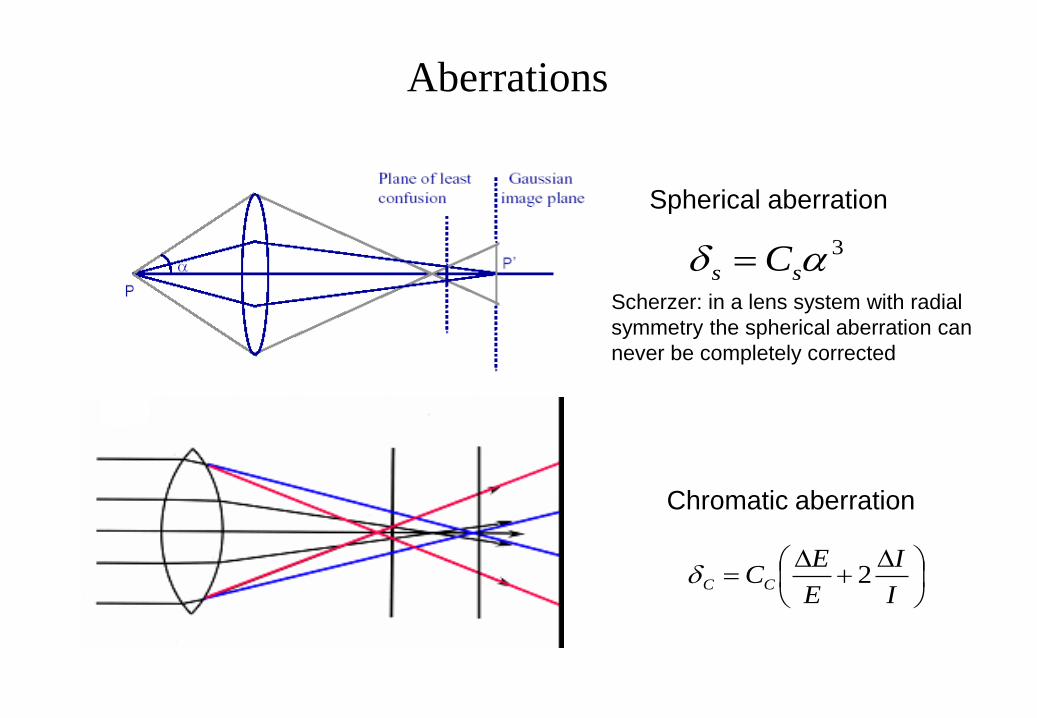
Aberrations
Spherical aberration
Chromatic aberration
I
I
E
ECCC 2
3 ss CScherzer: in a lens system with radial
symmetry the spherical aberration can
never be completely corrected
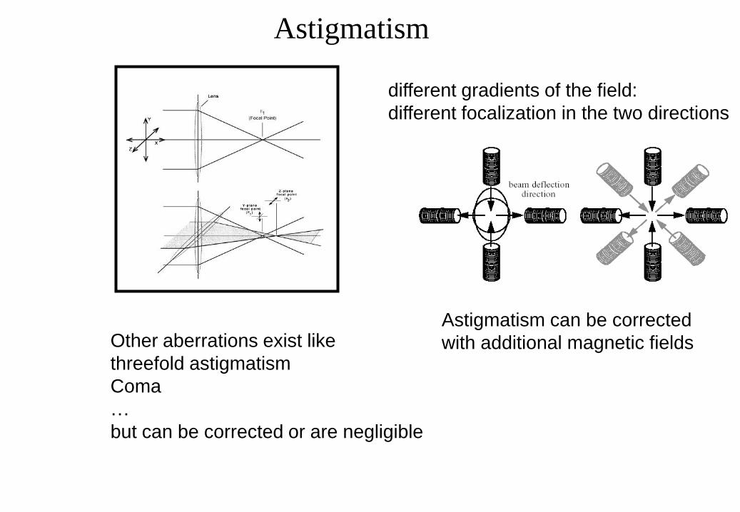
Astigmatism
different gradients of the field:
different focalization in the two directions
Astigmatism can be corrected
with additional magnetic fields Other aberrations exist like
threefold astigmatism
Coma
…
but can be corrected or are negligible
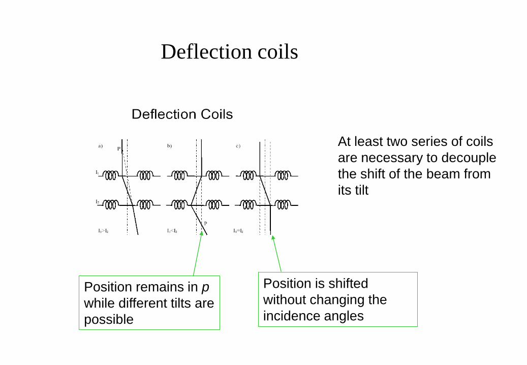
Deflection coils
At least two series of coils
are necessary to decouple
the shift of the beam from
its tilt
Position remains in p
while different tilts are
possible
Position is shifted
without changing the
incidence angles
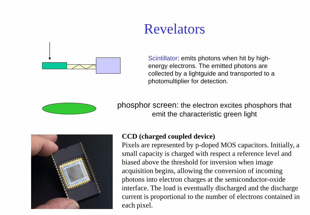
Revelators
Scintillator: emits photons when hit by high-
energy electrons. The emitted photons are
collected by a lightguide and transported to a
photomultiplier for detection.
phosphor screen: the electron excites phosphors that
emit the characteristic green light
CCD (charged coupled device)
Pixels are represented by p-doped MOS capacitors. Initially, a
small capacity is charged with respect a reference level and
biased above the threshold for inversion when image
acquisition begins, allowing the conversion of incoming
photons into electron charges at the semiconductor-oxide
interface. The load is eventually discharged and the discharge
current is proportional to the number of electrons contained in
each pixel.
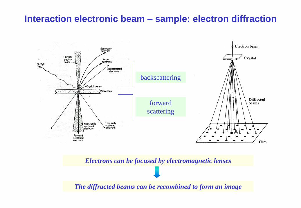
Interaction electronic beam – sample: electron diffraction
backscattering
forward
scattering
Electrons can be focused by electromagnetic lenses
The diffracted beams can be recombined to form an image
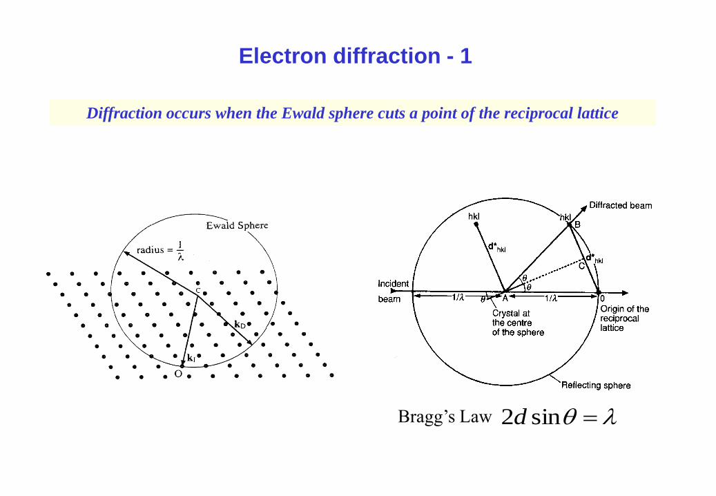
Electron diffraction - 1
l sin2dBragg’s Law
Diffraction occurs when the Ewald sphere cuts a point of the reciprocal lattice
l1
1 d
L
R
R
Ld
l
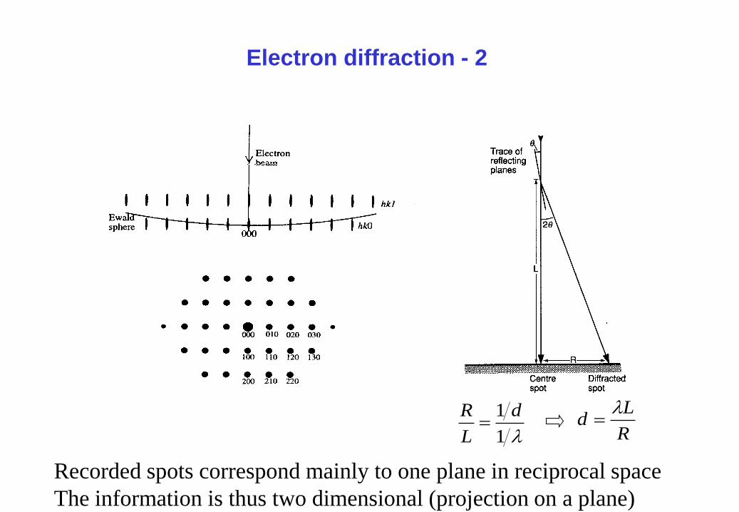
Electron diffraction - 2
Recorded spots correspond mainly to one plane in reciprocal space
The information is thus two dimensional (projection on a plane)
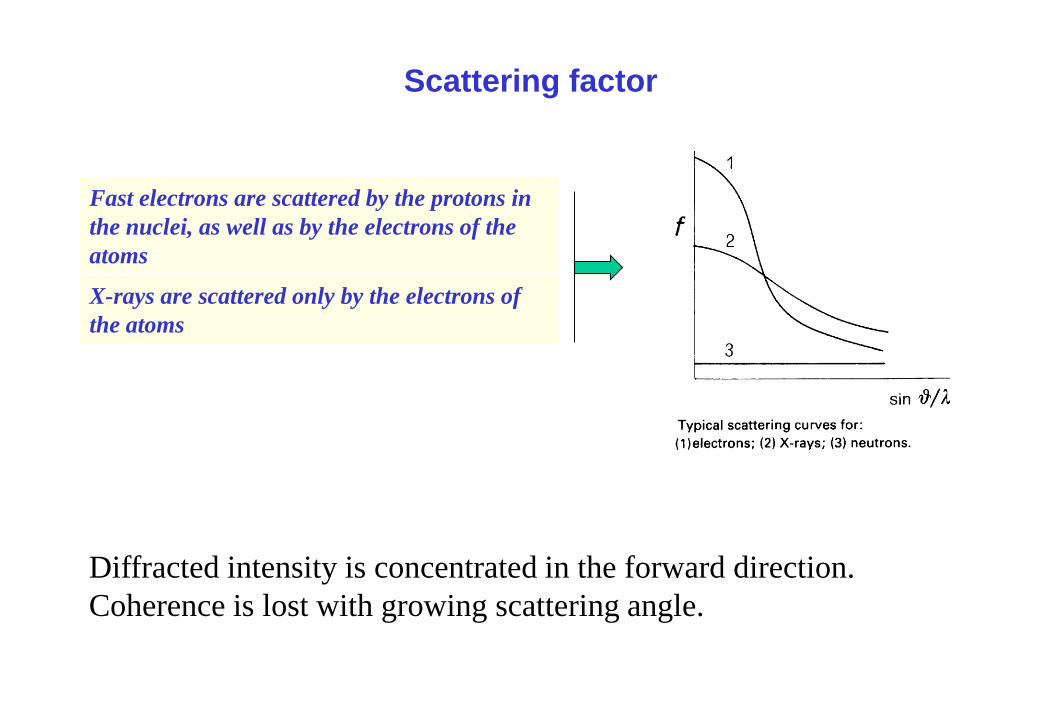
Scattering factor
Fast electrons are scattered by the protons in
the nuclei, as well as by the electrons of the
atoms
X-rays are scattered only by the electrons of
the atoms
Diffracted intensity is concentrated in the forward direction.
Coherence is lost with growing scattering angle.

X-ray (Cu K)
l = 154 pm
rE = 3.25·109 m
Electrons (200 kV)
l = 2.51 pm
rE = 2.0·1011 m
Comparison between high energy electron diffraction
and X-ray diffraction
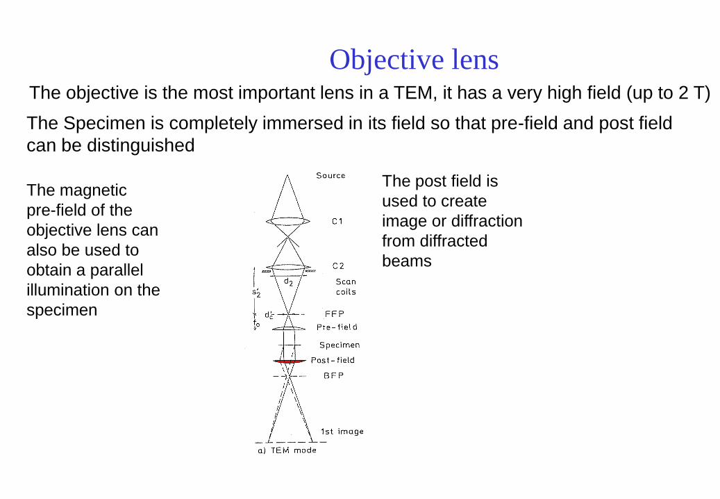
Objective lens
The magnetic
pre-field of the
objective lens can
also be used to
obtain a parallel
illumination on the
specimen
The objective is the most important lens in a TEM, it has a very high field (up to 2 T)
The Specimen is completely immersed in its field so that pre-field and post field
can be distinguished
The post field is
used to create
image or diffraction
from diffracted
beams
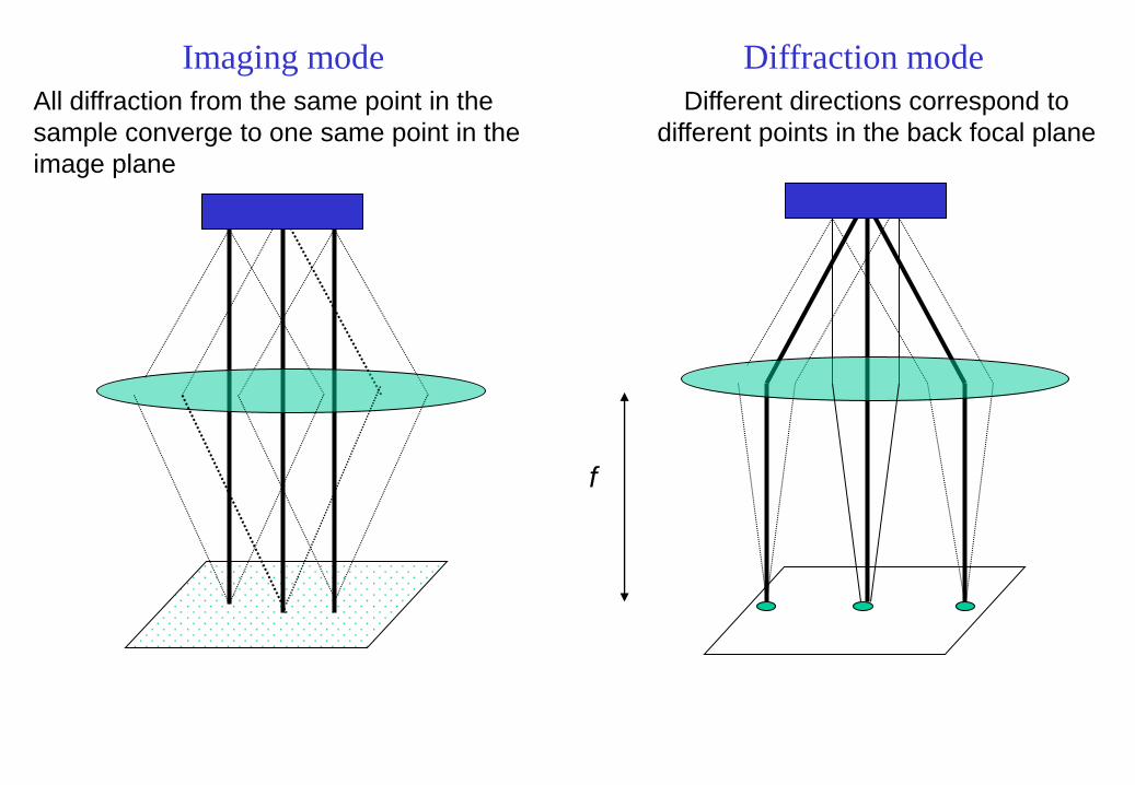
f
Different directions correspond to
different points in the back focal plane
Diffraction mode Imaging mode
All diffraction from the same point in the
sample converge to one same point in the
image plane
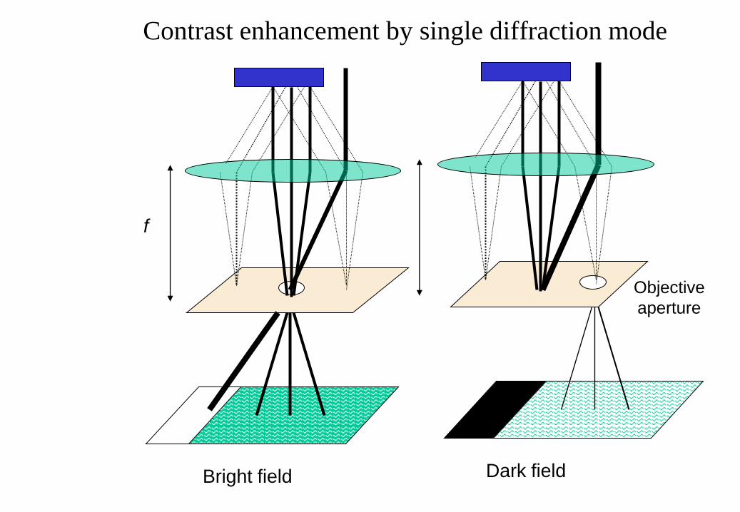
Contrast enhancement by single diffraction mode
Bright field Dark field
Objective
aperture
f
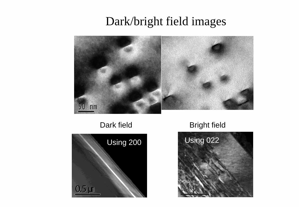
Dark/bright field images
Dark field Bright field
0.5 µm0.5 µm
Using 200 Using 022
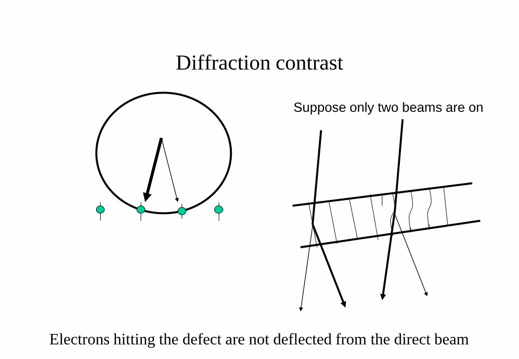
Diffraction contrast
Suppose only two beams are on
Electrons hitting the defect are not deflected from the direct beam
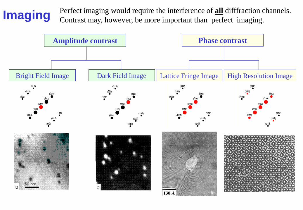
Imaging
Lattice Fringe Image High Resolution Image
Phase contrast Amplitude contrast
Bright Field Image Dark Field Image
Perfect imaging would require the interference of all difffraction channels.
Contrast may, however, be more important than perfect imaging.
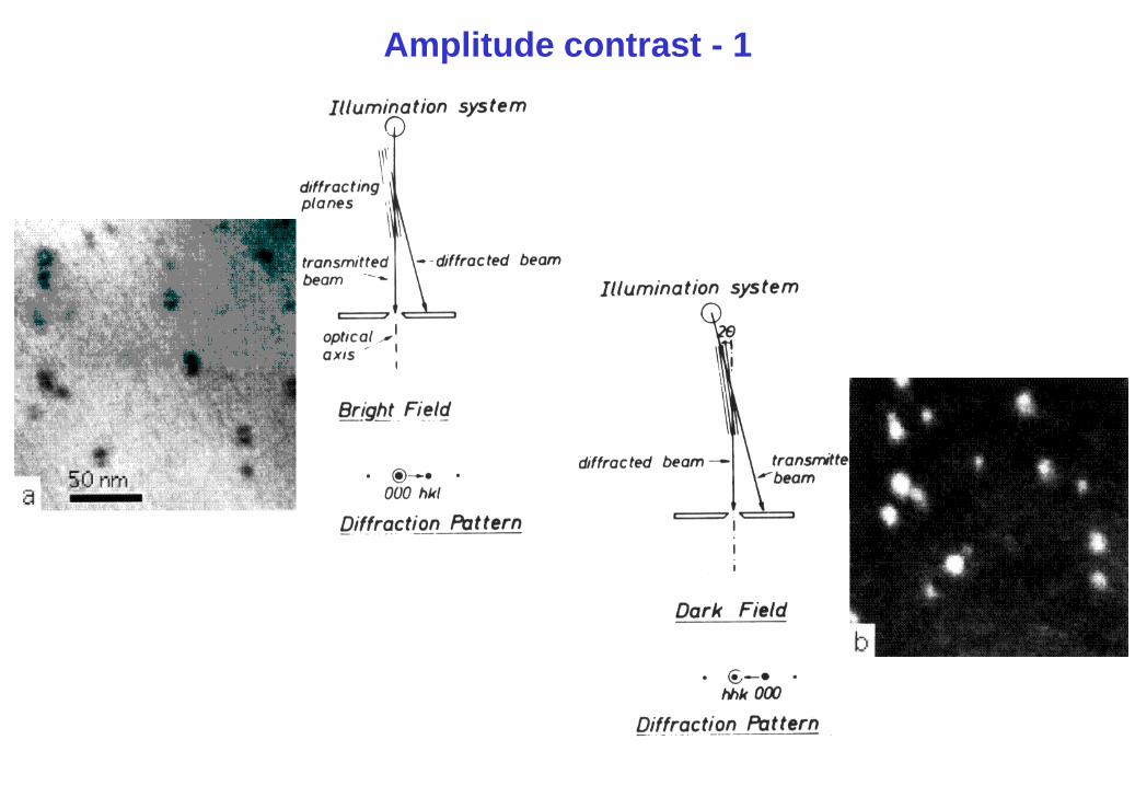
Amplitude contrast - 1
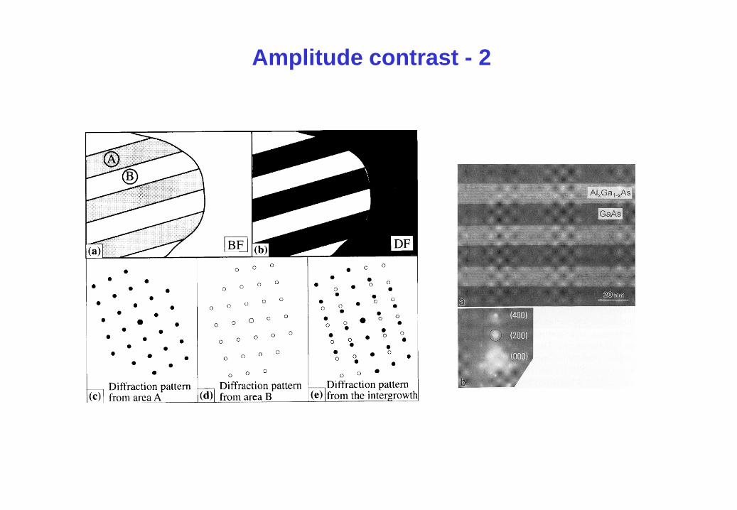
Amplitude contrast - 2

Fringes indicate two Dim. periodicity
Phase contrast in electron microscopy
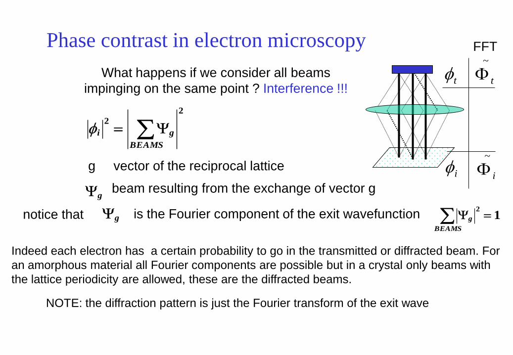
Phase contrast in electron microscopy
t
i
What happens if we consider all beams
impinging on the same point ? Interference !!!
~
t
~
i
FFT
2
2
BEAMS
gi
g vector of the reciprocal lattice
g beam resulting from the exchange of vector g
notice that g is the Fourier component of the exit wavefunction 12
BEAMS
g
Indeed each electron has a certain probability to go in the transmitted or diffracted beam. For
an amorphous material all Fourier components are possible but in a crystal only beams with
the lattice periodicity are allowed, these are the diffracted beams.
NOTE: the diffraction pattern is just the Fourier transform of the exit wave
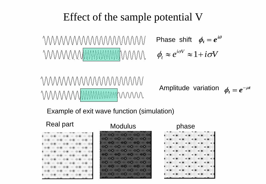
Effect of the sample potential V
Phase shift
Amplitude variation
it e
tt e
Example of exit wave function (simulation)
Real part Modulus phase
Vie Vi
t 1
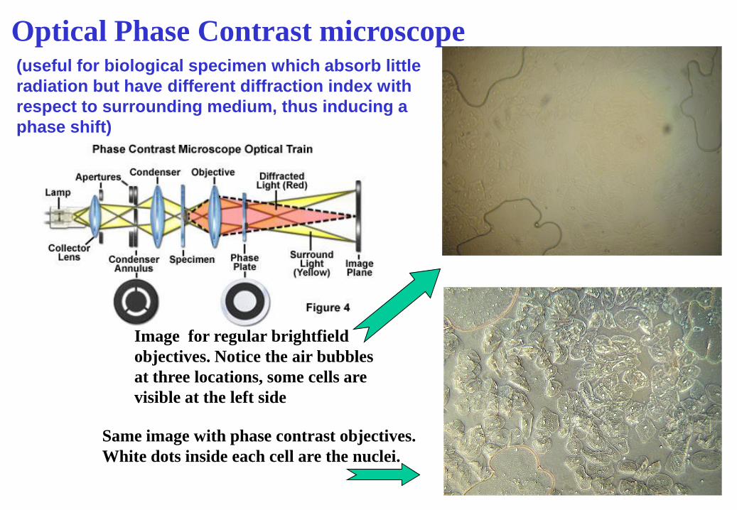
(useful for biological specimen which absorb little
radiation but have different diffraction index with
respect to surrounding medium, thus inducing a
phase shift)
Image for regular brightfield
objectives. Notice the air bubbles
at three locations, some cells are
visible at the left side
Same image with phase contrast objectives.
White dots inside each cell are the nuclei.
Optical Phase Contrast microscope
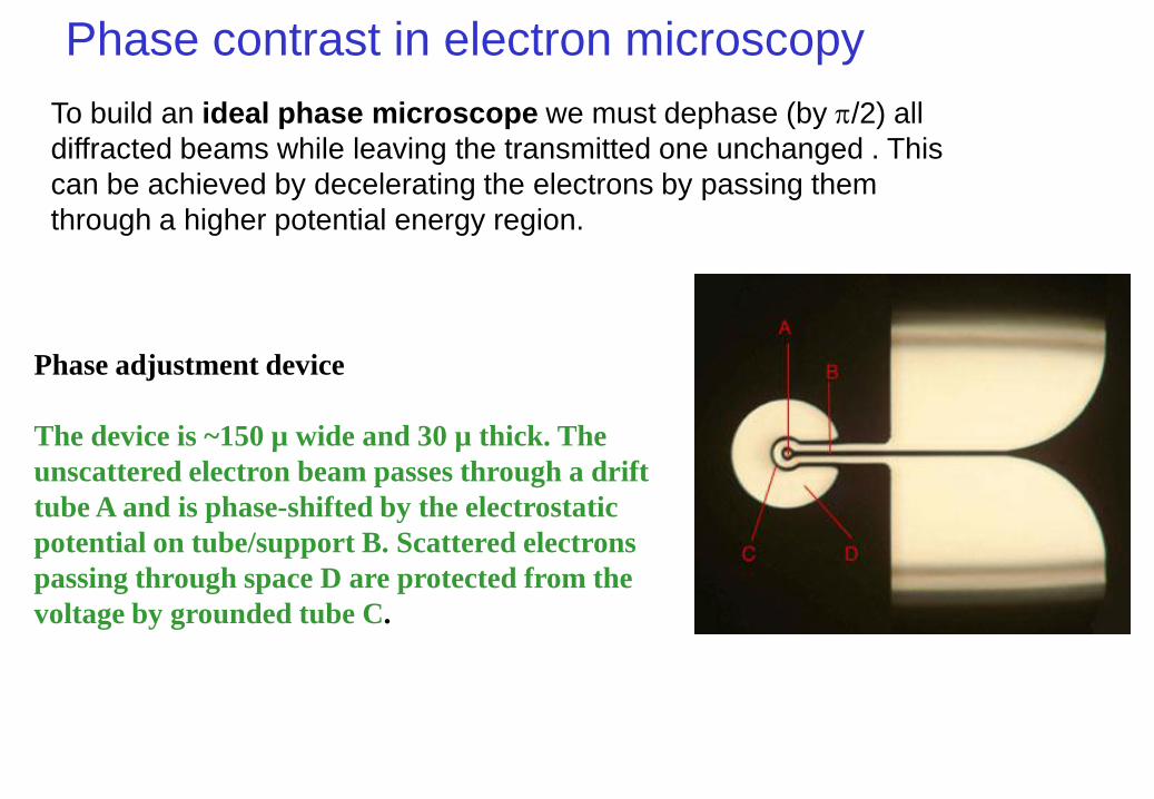
To build an ideal phase microscope we must dephase (by /2) all
diffracted beams while leaving the transmitted one unchanged . This
can be achieved by decelerating the electrons by passing them
through a higher potential energy region.
Phase adjustment device
The device is ~150 µ wide and 30 µ thick. The
unscattered electron beam passes through a drift
tube A and is phase-shifted by the electrostatic
potential on tube/support B. Scattered electrons
passing through space D are protected from the
voltage by grounded tube C.
Phase contrast in electron microscopy
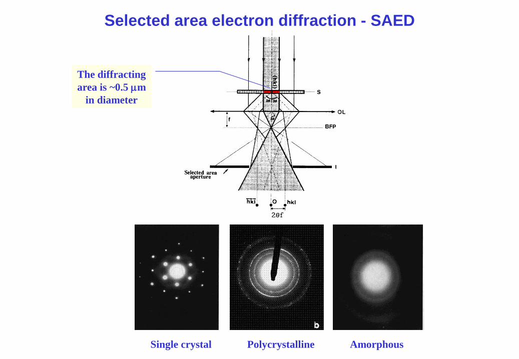
Selected area electron diffraction - SAED
The diffracting
area is ~0.5 m
in diameter
Single crystal Polycrystalline Amorphous
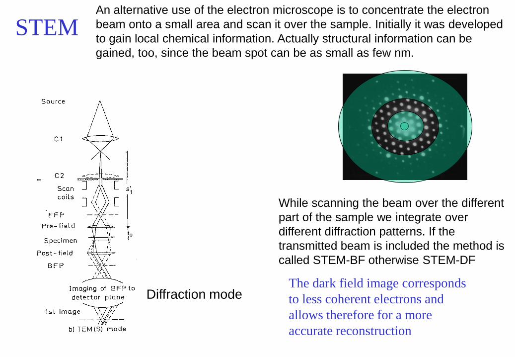
Diffraction mode
While scanning the beam over the different
part of the sample we integrate over
different diffraction patterns. If the
transmitted beam is included the method is
called STEM-BF otherwise STEM-DF
An alternative use of the electron microscope is to concentrate the electron
beam onto a small area and scan it over the sample. Initially it was developed
to gain local chemical information. Actually structural information can be
gained, too, since the beam spot can be as small as few nm.
STEM
The dark field image corresponds
to less coherent electrons and
allows therefore for a more
accurate reconstruction
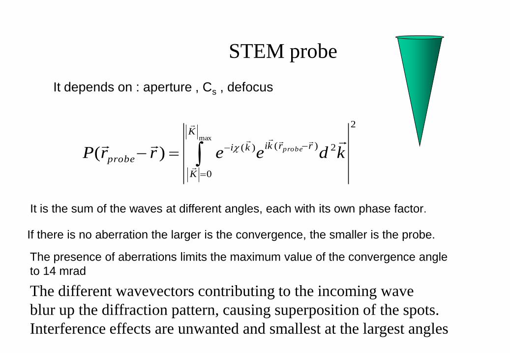
STEM probe
It depends on : aperture , Cs , defocus
2
0
2)()(max
)(
K
K
rrkiki
probe kdeerrP probe
It is the sum of the waves at different angles, each with its own phase factor.
If there is no aberration the larger is the convergence, the smaller is the probe.
The presence of aberrations limits the maximum value of the convergence angle
to 14 mrad
The different wavevectors contributing to the incoming wave
blur up the diffraction pattern, causing superposition of the spots.
Interference effects are unwanted and smallest at the largest angles
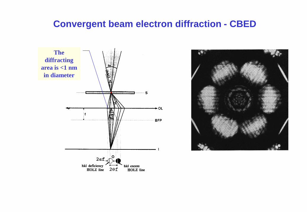
Convergent beam electron diffraction - CBED
The
diffracting
area is <1 nm
in diameter
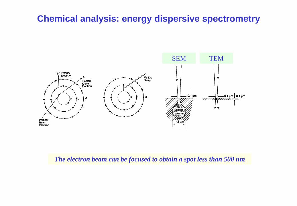
Chemical analysis: energy dispersive spectrometry
The electron beam can be focused to obtain a spot less than 500 nm
SEM TEM

http://www.gel.usherbrooke.ca/casino/download2.html
Energy released in the matrix
GaAs
bulk
Trajectories of 100 KeV Trajectories of 10 KeV
GaAs
thin film
Probed volume
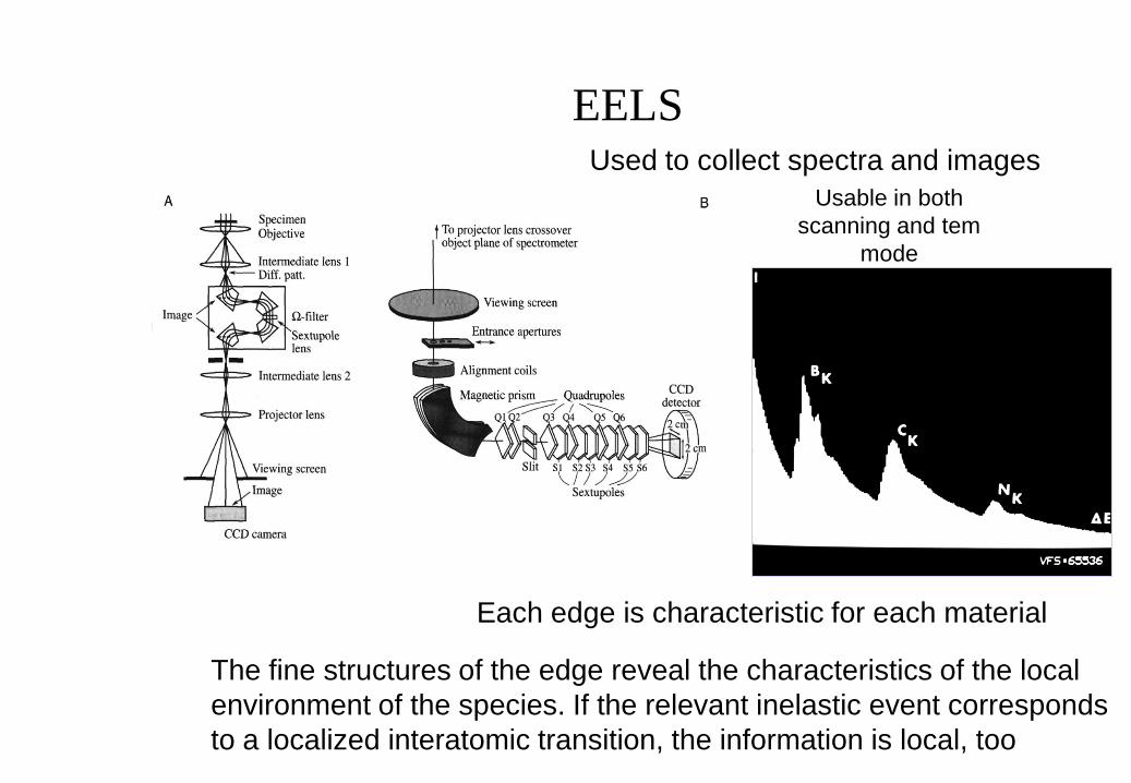
EELS Used to collect spectra and images
Usable in both
scanning and tem
mode
Each edge is characteristic for each material
The fine structures of the edge reveal the characteristics of the local
environment of the species. If the relevant inelastic event corresponds
to a localized interatomic transition, the information is local, too
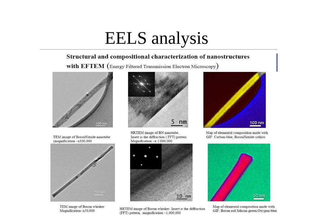
EELS analysis

Tomography By observing at
different angle it
it is possible to
reconstruct the
3D image
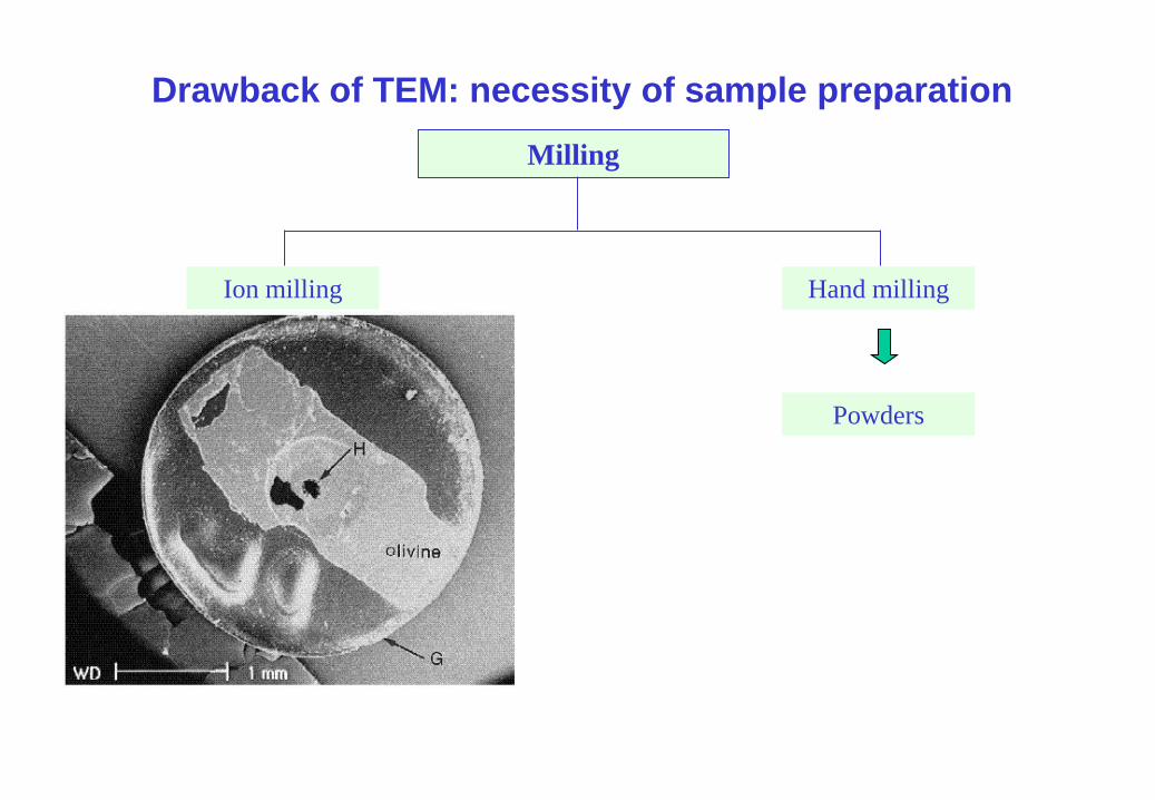
Drawback of TEM: necessity of sample preparation
Ion milling
Milling
Hand milling
Powders
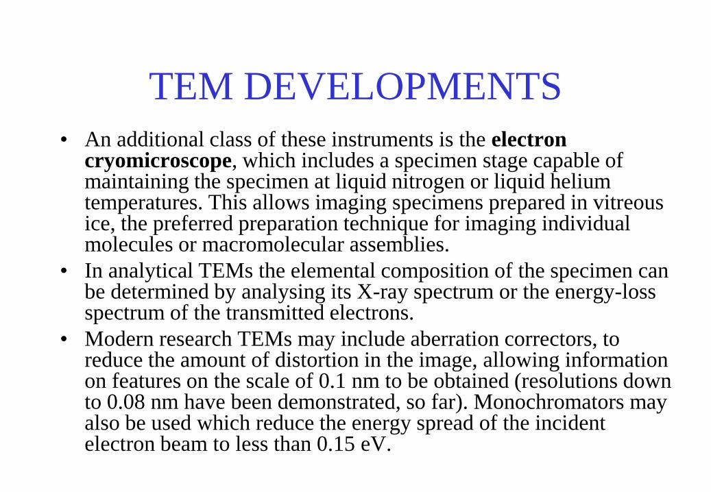
TEM DEVELOPMENTS
• An additional class of these instruments is the electron cryomicroscope, which includes a specimen stage capable of maintaining the specimen at liquid nitrogen or liquid helium temperatures. This allows imaging specimens prepared in vitreous ice, the preferred preparation technique for imaging individual molecules or macromolecular assemblies.
• In analytical TEMs the elemental composition of the specimen can be determined by analysing its X-ray spectrum or the energy-loss spectrum of the transmitted electrons.
• Modern research TEMs may include aberration correctors, to reduce the amount of distortion in the image, allowing information on features on the scale of 0.1 nm to be obtained (resolutions down to 0.08 nm have been demonstrated, so far). Monochromators may also be used which reduce the energy spread of the incident electron beam to less than 0.15 eV.
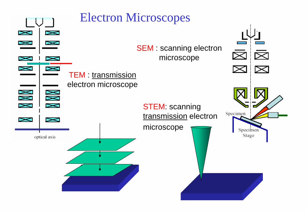
TEM : transmission
electron microscope
SEM : scanning electron
microscope
STEM: scanning
transmission electron
microscope
Electron Microscopes
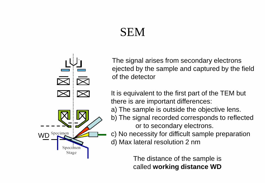
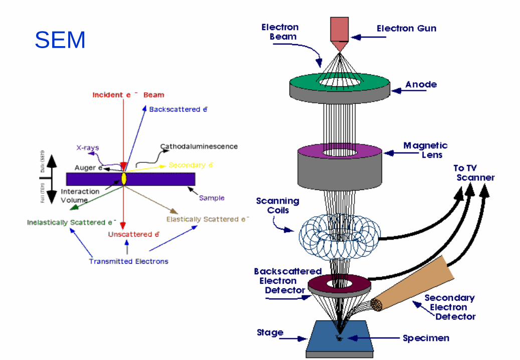
SEM
The signal arises from secondary electrons
ejected by the sample and captured by the field
of the detector
It is equivalent to the first part of the TEM but
there is are important differences:
a) The sample is outside the objective lens.
b) The signal recorded corresponds to reflected
or to secondary electrons.
c) No necessity for difficult sample preparation
d) Max lateral resolution 2 nm
The distance of the sample is
called working distance WD
WD
SEM
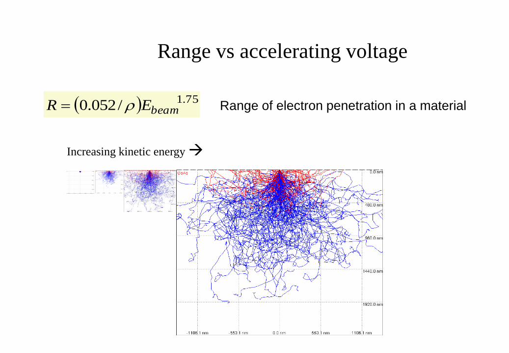
Range vs accelerating voltage
75.1/052.0 beamER Range of electron penetration in a material
Increasing kinetic energy
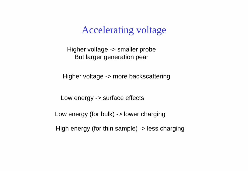
Accelerating voltage
Higher voltage -> smaller probe
But larger generation pear
Higher voltage -> more backscattering
Low energy -> surface effects
Low energy (for bulk) -> lower charging
High energy (for thin sample) -> less charging
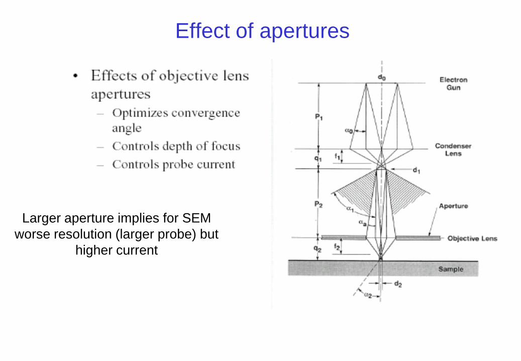
Effect of apertures
Larger aperture implies for SEM
worse resolution (larger probe) but
higher current

Effect of Strength of Condenser Lens
The effect is similar to that
of changing the aperture
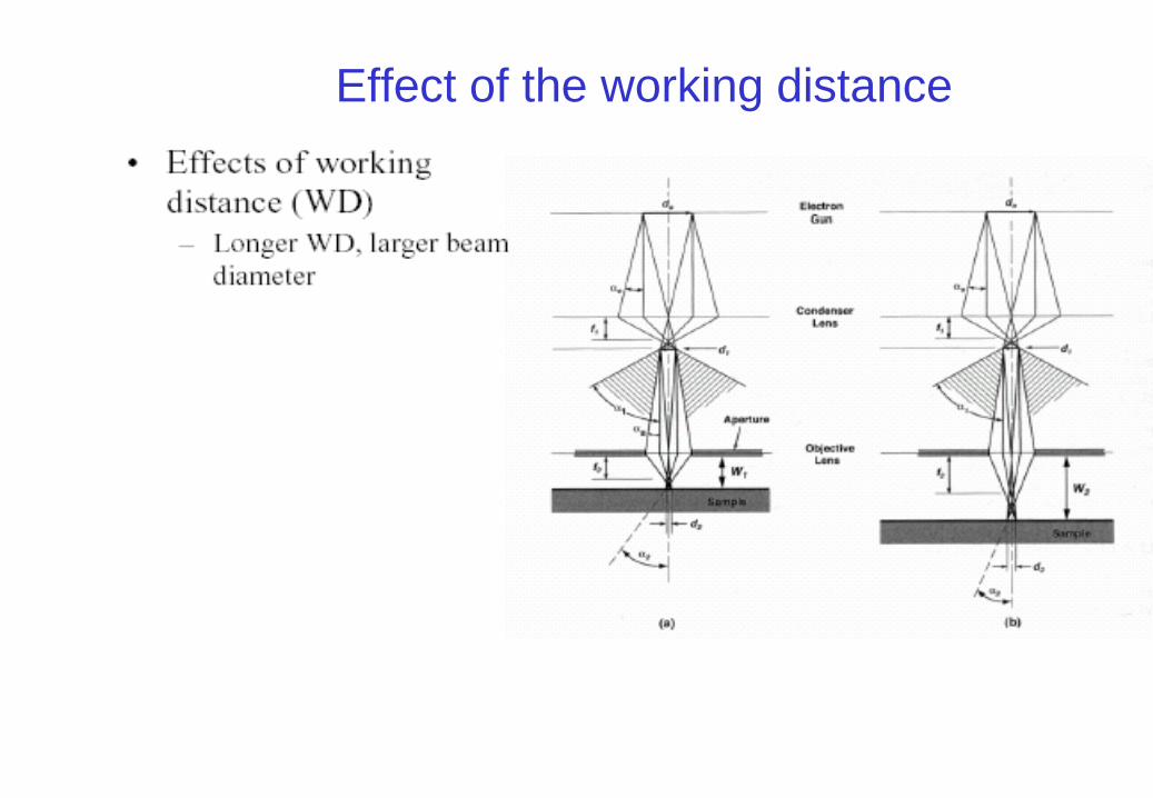
Effect of the working distance

Depth of field D
D
WD
WD
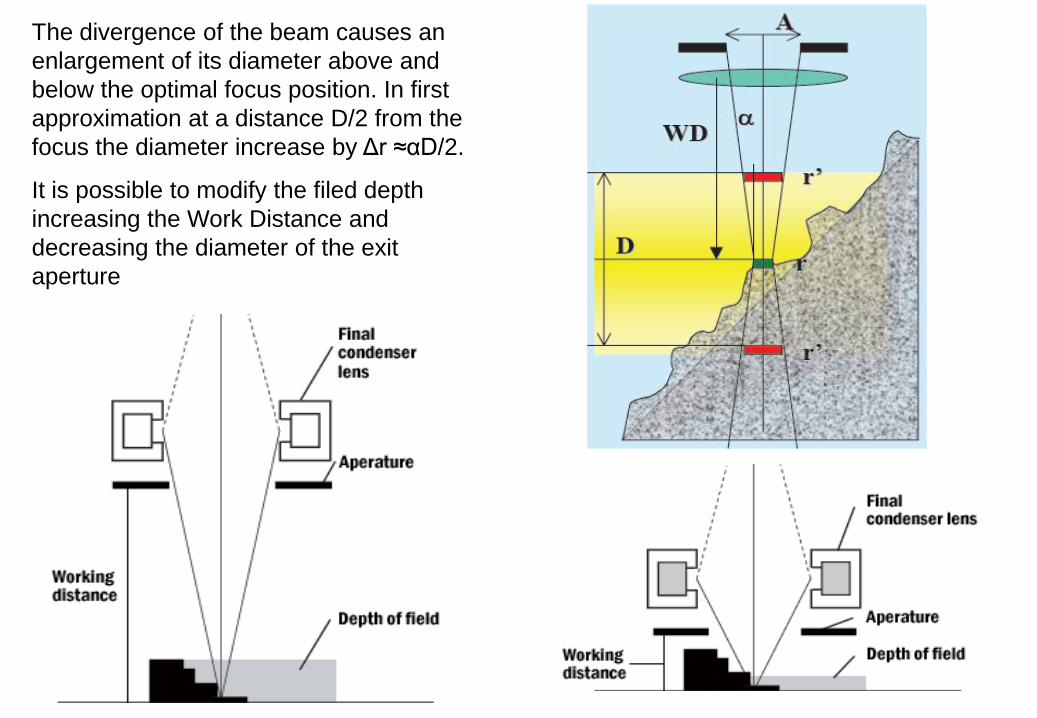
The divergence of the beam causes an
enlargement of its diameter above and
below the optimal focus position. In first
approximation at a distance D/2 from the
focus the diameter increase by Δr ≈αD/2.
It is possible to modify the filed depth
increasing the Work Distance and
decreasing the diameter of the exit
aperture
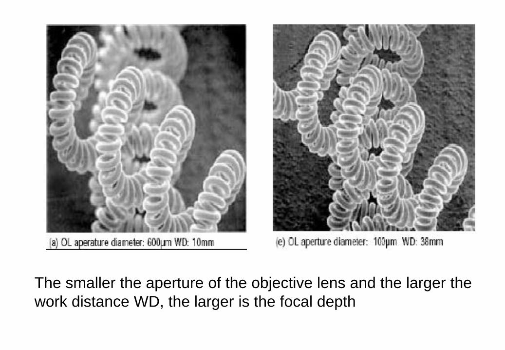
The smaller the aperture of the objective lens and the larger the
work distance WD, the larger is the focal depth
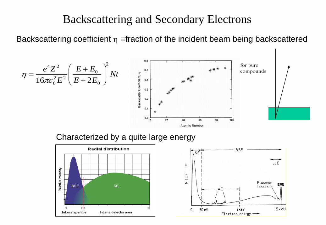
Backscattering and Secondary Electrons
NtEE
EE
E
Ze2
0
0
22
0
24
216
Backscattering coefficient =fraction of the incident beam being backscattered
Characterized by a quite large energy
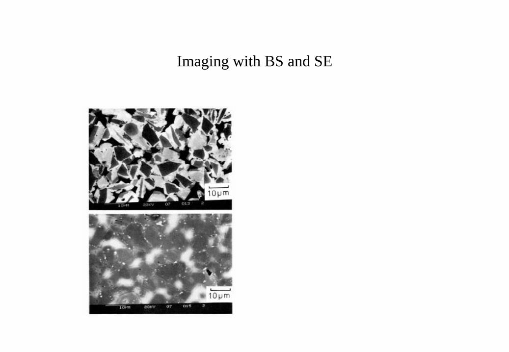
Imaging with BS and SE
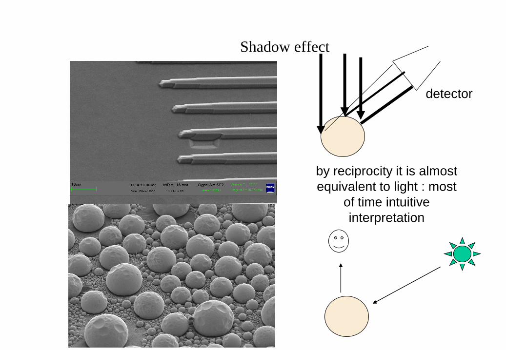
Shadow effect
detector
by reciprocity it is almost
equivalent to light : most
of time intuitive
interpretation

Kikuchi patterns
Kikuchi lines are formed in diffraction patterns by inelastic diffusely scattered electrons,
e.g. as a result of thermal atom vibrations. The main features of their geometry can be
deduced from a simple elastic mechanism proposed in 1928 by Seishi Kikuchi although
the dynamical theory of diffuse inelastic scattering is needed to understand them
quantitatively. In x-ray scattering the equivalent lines are referred to as Kossel lines.
Kikuchi patterns are
strongest when the
electron diffraction is
weakest, eg. at high
energy and high
crystal temperature
Kikuchi patterns in
LEED:
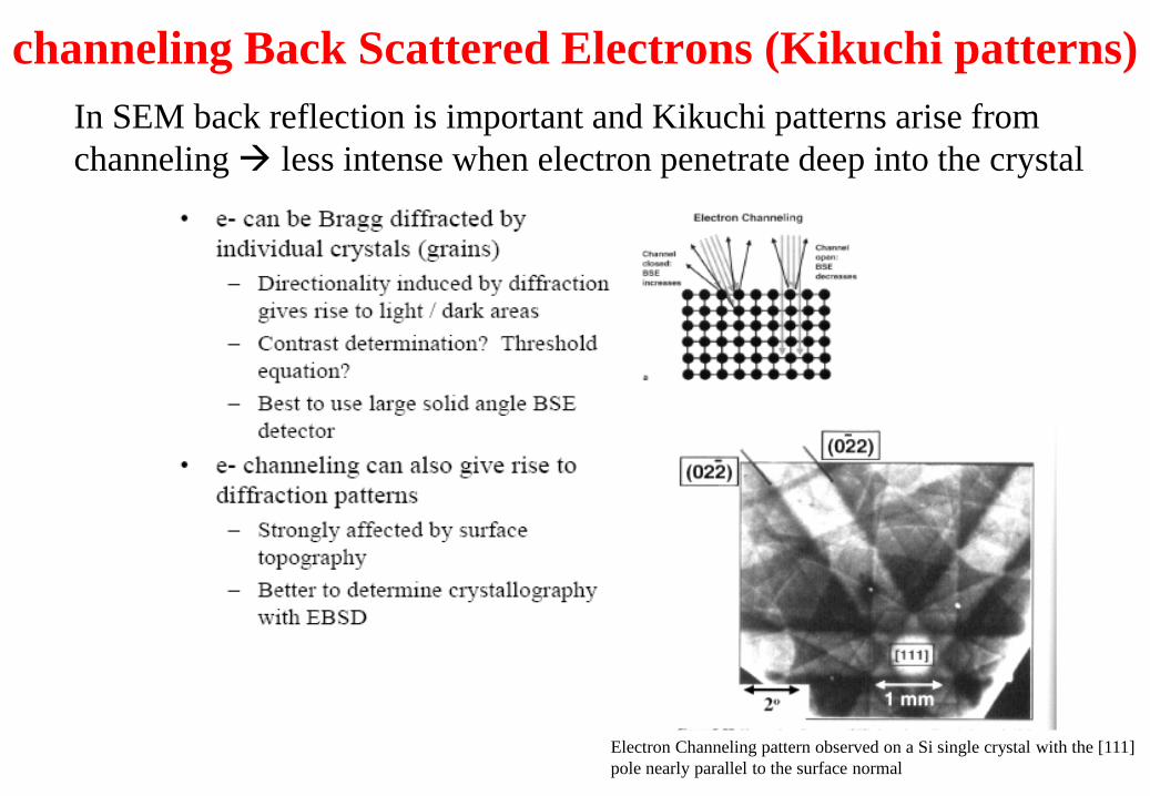
Electron Channeling pattern observed on a Si single crystal with the [111]
pole nearly parallel to the surface normal
In SEM back reflection is important and Kikuchi patterns arise from
channeling less intense when electron penetrate deep into the crystal
channeling Back Scattered Electrons (Kikuchi patterns)

BSDE Backscattering electron diffraction
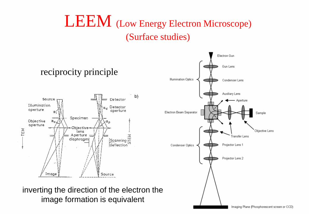
inverting the direction of the electron the
image formation is equivalent
reciprocity principle
LEEM (Low Energy Electron Microscope)
(Surface studies)
LEEM (Low Energy Electron Microscope)
(allows for surface studies)
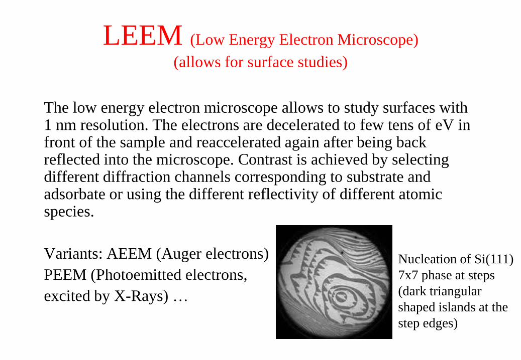
The low energy electron microscope allows to study surfaces with 1 nm resolution. The electrons are decelerated to few tens of eV in front of the sample and reaccelerated again after being back reflected into the microscope. Contrast is achieved by selecting different diffraction channels corresponding to substrate and adsorbate or using the different reflectivity of different atomic species.
Variants: AEEM (Auger electrons)
PEEM (Photoemitted electrons,
excited by X-Rays) …
Nucleation of Si(111)
7x7 phase at steps
(dark triangular
shaped islands at the
step edges)


![Electron Microscopy - Wikis09-10]_DOWNLOAD/4 tem i.… · Electron Microscopy 4. TEM Basics: interactions, basic modes, sample preparation, Diffraction: elastic scattering theory,](https://static.fdocuments.us/doc/165x107/5f05009e7e708231d410c617/electron-microscopy-wikis-09-10download4-tem-i-electron-microscopy-4-tem.jpg)