ECE 301 – Digital Electronics Flip-Flops and Registers (Lecture #15)

Flip-Flops and Registers
(Lecture #19)
The slides included herein were taken from the materials accompanying
Fundamentals of Logic Design, 6th Edition, by Roth and Kinney,
and were used with permission from Cengage Learning.

Spring 2011 ECE 331 - Digital System Design 2
Flip-Flops
(continued)
Spring 2011 ECE 331 - Digital System Design 3
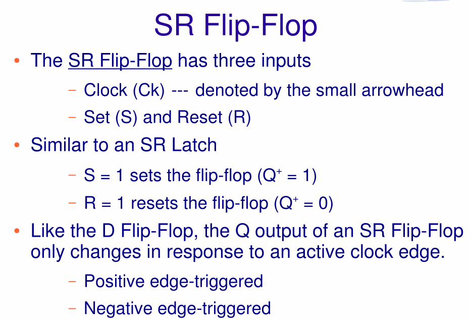
SR Flip-Flop● The SR Flip-Flop has three inputs
– Clock (Ck) --- denoted by the small arrowhead
– Set (S) and Reset (R)
● Similar to an SR Latch
– S = 1 sets the flip-flop (Q+ = 1)
– R = 1 resets the flip-flop (Q+ = 0)
● Like the D Flip-Flop, the Q output of an SR Flip-Flop only changes in response to an active clock edge.
– Positive edge-triggered
– Negative edge-triggered

Spring 2011 ECE 331 - Digital System Design 4
SR Flip-Flop
S R Q Q+
0 0 0 0
0 0 1 1
0 1 0 0
0 1 1 0
1 0 0 1
1 0 1 1
1 1 0 not
1 1 1 allowed
}Q+ = Q
Q+ = 0
Q+ = 1set
reset
store
}}
positive edge-triggeredSR Flip-Flop
State change occurs after active Clock edge

Spring 2011 ECE 331 - Digital System Design 5
SR Flip-Flop (master-slave)
Enabled on opposite levels of the clock
SR Latches

Spring 2011 ECE 331 - Digital System Design 6
SR Flip-Flop: Timing Diagram

Spring 2011 ECE 331 - Digital System Design 7
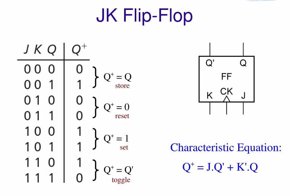
JK Flip-Flop● The JK Flip-Flop has three inputs
– Clock (Ck) --- denoted by the small arrowhead
– J and K
● Similar to the SR Flip-Flop
– J corresponds to S: J = 1 → Q+ = 1
– K corresponds to R: K = 1 → Q+ = 0
● Different from the SR Flip-Flop in that the input combination J = 1, K = 1 is allowed.
– J = K = 1 causes the Q output to toggle after an active clock edge.
Spring 2011 ECE 331 - Digital System Design 8
JK Flip-Flop
}Q+ = Q
}Q+ = 0
}Q+ = 1
}Q+ = Q'
set
reset
store
toggle
Q+ = J.Q' + K'.Q
Characteristic Equation:

Spring 2011 ECE 331 - Digital System Design 9
JK Flip-Flop (master-slave)
SR Latches
Enabled on opposite levels of the clock
Spring 2011 ECE 331 - Digital System Design 10
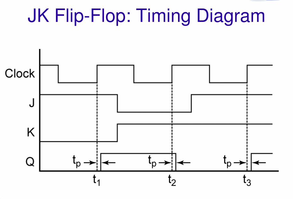
JK Flip-Flop: Timing Diagram

Spring 2011 ECE 331 - Digital System Design 11
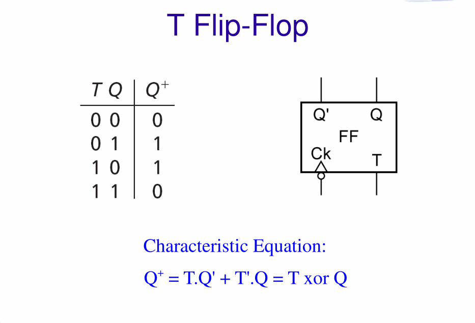
T Flip-Flop
● The Toggle (T) Flip-Flop has two inputs
– Clock (Ck) --- denoted by the small arrowhead
– Toggle (T)
● The T input controls the state change
– when T = 0, the state does not change (Q+ = Q)
– when T = 1, the state changes following an active clock edge (Q+ = Q')
● T Flip-Flops are often used in the design of counters.
Spring 2011 ECE 331 - Digital System Design 12
T Flip-Flop
Q+ = T.Q' + T'.Q = T xor Q
Characteristic Equation:
Spring 2011 ECE 331 - Digital System Design 13
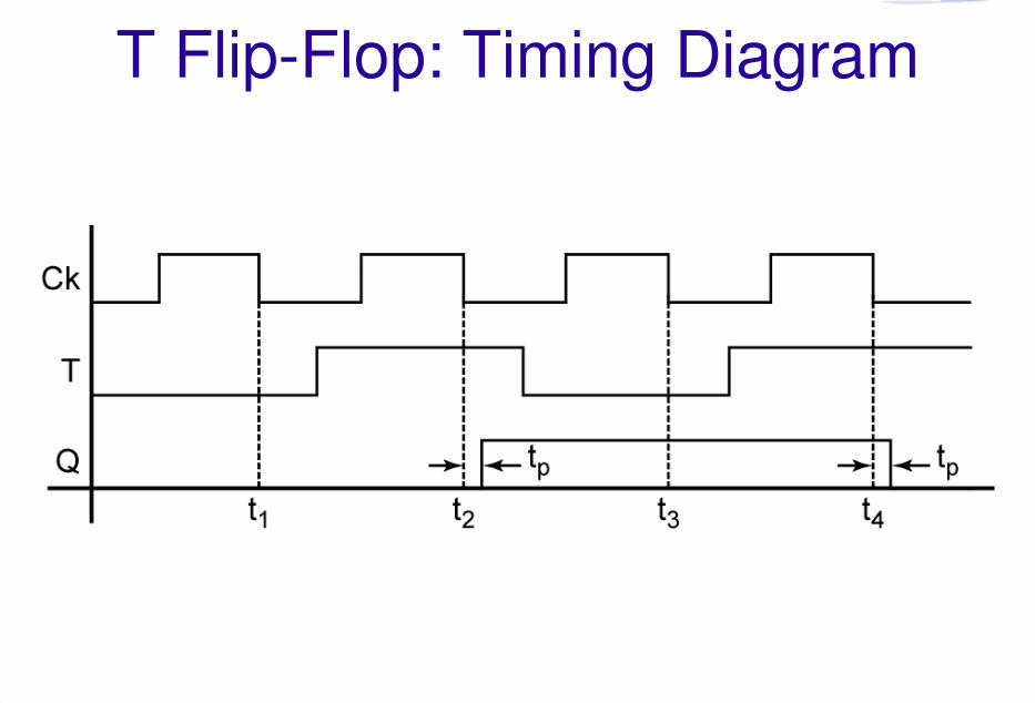
T Flip-Flop: Timing Diagram

Spring 2011 ECE 331 - Digital System Design 14
Building a T Flip-Flop

Spring 2011 ECE 331 - Digital System Design 15
Asynchronous Control Signals

Spring 2011 ECE 331 - Digital System Design 16
Asynchronous Control Signals: Timing Diagram

Spring 2011 ECE 331 - Digital System Design 17
D FF with Clock Enable

Spring 2011 ECE 331 - Digital System Design 18
Flip-Flops in VHDL
Spring 2011 ECE 331 - Digital System Design 19
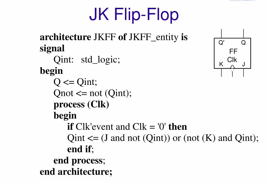
JK Flip-Floparchitecture JKFF of JKFF_entity is
signal
Qint: std_logic;
beginQ <= Qint;Qnot <= not (Qint);
process (Clk)
begin
if Clk'event and Clk = '0' thenQint <= (J and not (Qint)) or (not (K) and Qint);
end if;
end process;
end architecture;
FF
Clk
Spring 2011 ECE 331 - Digital System Design 20
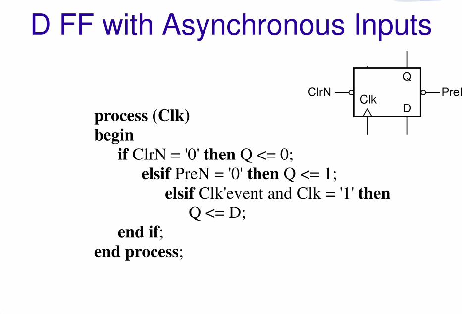
D FF with Asynchronous Inputs
process (Clk)
begin
if ClrN = '0' then Q <= 0;
elsif PreN = '0' then Q <= 1;
elsif Clk'event and Clk = '1' then
Q <= D;
end if;
end process;
Clk

Spring 2011 ECE 331 - Digital System Design 21
Registers

Spring 2011 ECE 331 - Digital System Design 22
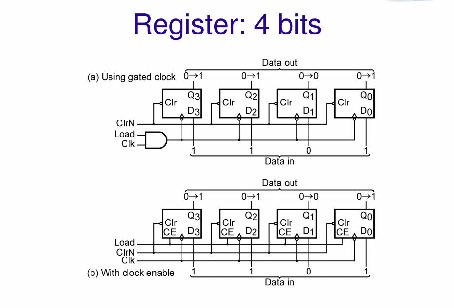
Several D flip-flops may be grouped together with a common
clock to form a register. Because each flip-flop can store one
bit of information, a register with n D flip-flops can store n bits
of information.
A load signal can be ANDed with the clock to enable and
disable loading the registers.
A better approach is to use registers with clock enables if
they are available.
Registers
Spring 2011 ECE 331 - Digital System Design 23
Register: 4 bits

Spring 2011 ECE 331 - Digital System Design 24
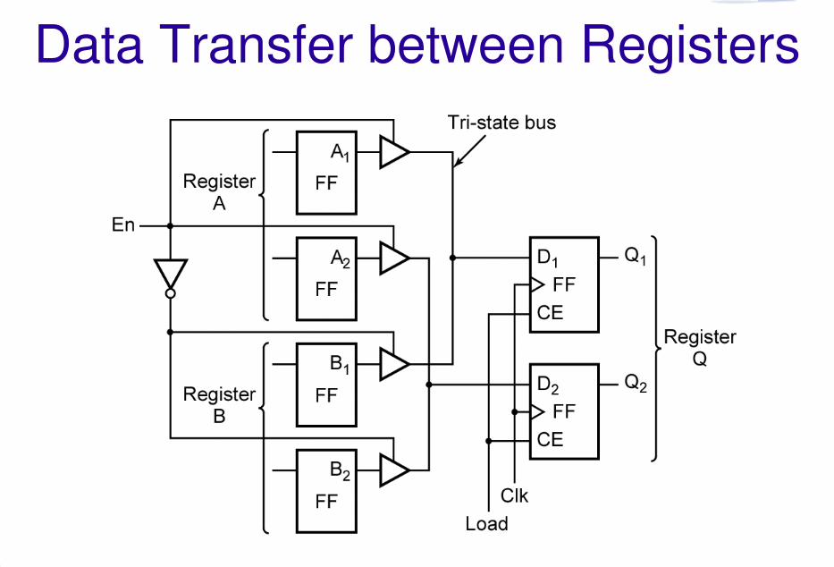
Data Transfer between Registers
● Data transfer between registers is a common operation in computer (i.e. digital) systems.
● Multiple registers can be interconnected using tri-state buffers.
● Data can be transferred between two registers by enabling the proper tri-state buffer.
Spring 2011 ECE 331 - Digital System Design 25
Data Transfer between Registers

Spring 2011 ECE 331 - Digital System Design 26
Register with Tri-state Output

Spring 2011 ECE 331 - Digital System Design 27
Data Transfer using Tri-state Bus

Spring 2011 ECE 331 - Digital System Design 28
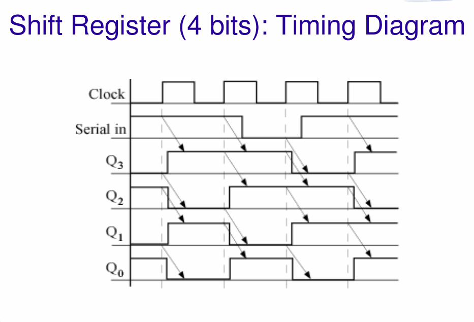
A shift register is a register in which binary data can be stored
and shifted either left or right. The data is shifted according to
the applied shift signal; often there is a left shift signal and a
right shift signal.
A shift register must be constructed using flip-flops (i.e. edge-
triggered devices); it cannot be constructed using latches or
gated-latches (i.e. level-sensitive devices).
Shift Register

Spring 2011 ECE 331 - Digital System Design 29
Shift Register: 4 bits
Spring 2011 ECE 331 - Digital System Design 30
Shift Register (4 bits): Timing Diagram

Spring 2011 ECE 331 - Digital System Design 31
8-bit SI SO Shift Register
Spring 2011 ECE 331 - Digital System Design 32
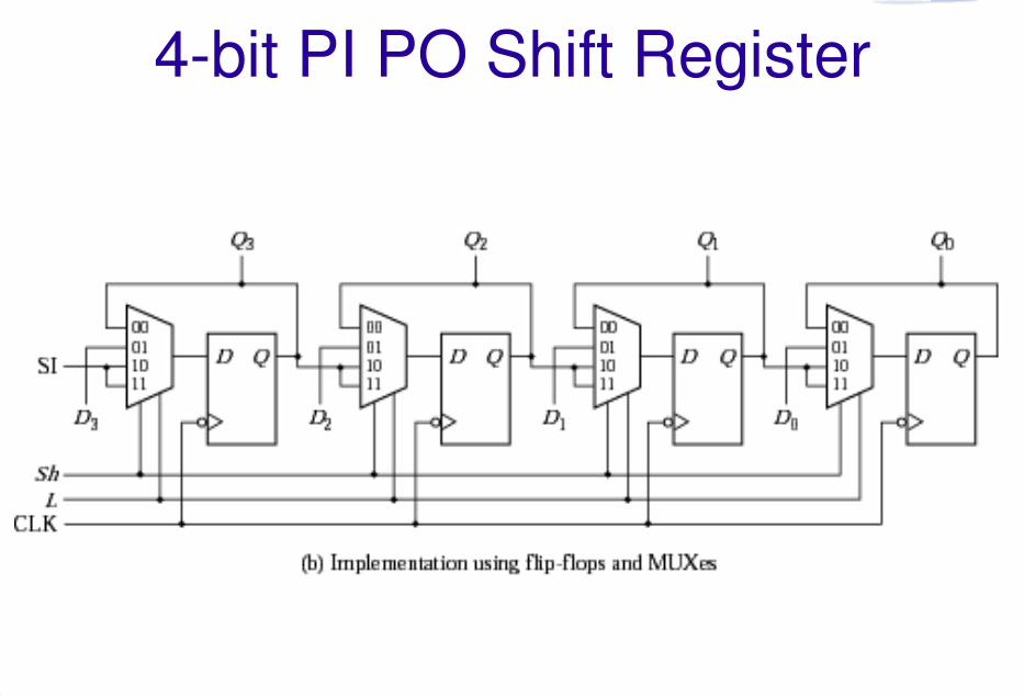
4-bit PI PO Shift Register
Spring 2011 ECE 331 - Digital System Design 33
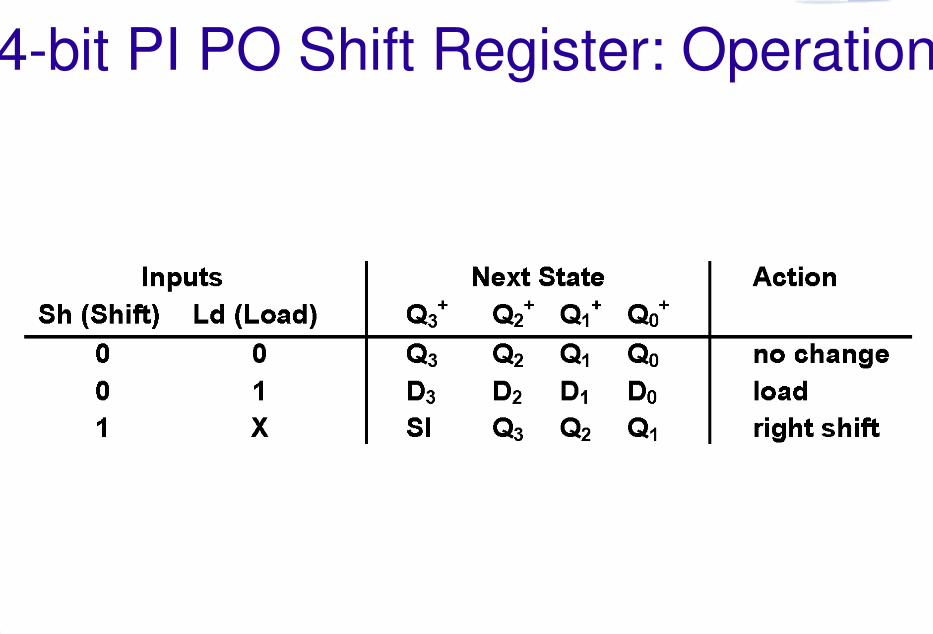
4-bit PI PO Shift Register: Operation

Spring 2011 ECE 331 - Digital System Design 34
Registers in VHDL
Spring 2011 ECE 331 - Digital System Design 35
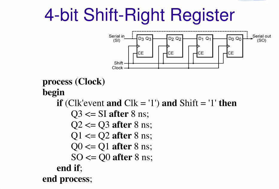
4-bit Shift-Right Register
process (Clock)
begin
if (Clk'event and Clk = '1') and Shift = '1' then
Q3 <= SI after 8 ns;
Q2 <= Q3 after 8 ns;
Q1 <= Q2 after 8 ns;
Q0 <= Q1 after 8 ns;
SO <= Q0 after 8 ns;
end if;
end process;
Spring 2011 ECE 331 - Digital System Design 36
Parallel Adder with Accumulator

Spring 2011 ECE 331 - Digital System Design 37
In computer circuits, it is frequently desirable to store one
number in a register (called an accumulator) and add a
second number to it, leaving the result stored in the register.
Parallel Adder with Accumulator
Spring 2011 ECE 331 - Digital System Design 38
n-bit Parallel Adder with Accumulator

Spring 2011 ECE 331 - Digital System Design 39
Before addition in the previous circuit can take place, the
accumulator must be loaded with X. This can be
accomplished in several ways. The easiest way is to first
clear the accumulator using the asynchronous clear inputs
on the flip-flops, and then put the X data on the Y inputs to
the adder and add the accumulator in the normal way.
Alternatively, we could add multiplexers at the accumulator
inputs so that we could select either the Y input data or the
adder output to load into the accumulator.
Loading the Accumulator
Spring 2011 ECE 331 - Digital System Design 40
Adder Cell with Multiplexer

Spring 2011 ECE 331 - Digital System Design 41
Questions?