Latches, Flip-flops, Registers, Memorycs240/f19/slides/registers.pdfC.8 Memory Elements: Flip-Flops,...
19
Latches, Flip-flops, Registers, Memory Sequential logic: elements to store values Output depends on inputs and stored values. (vs. combinational logic: output depends only on inputs) Latch: CC-BY Rberteig@flickr
Transcript of Latches, Flip-flops, Registers, Memorycs240/f19/slides/registers.pdfC.8 Memory Elements: Flip-Flops,...
Latches, Flip-flops,Registers, Memory
Sequential logic: elements to store valuesOutput depends on inputs and stored values.
(vs. combinational logic: output depends only on inputs)
Latch: CC-BY Rberteig@flickr
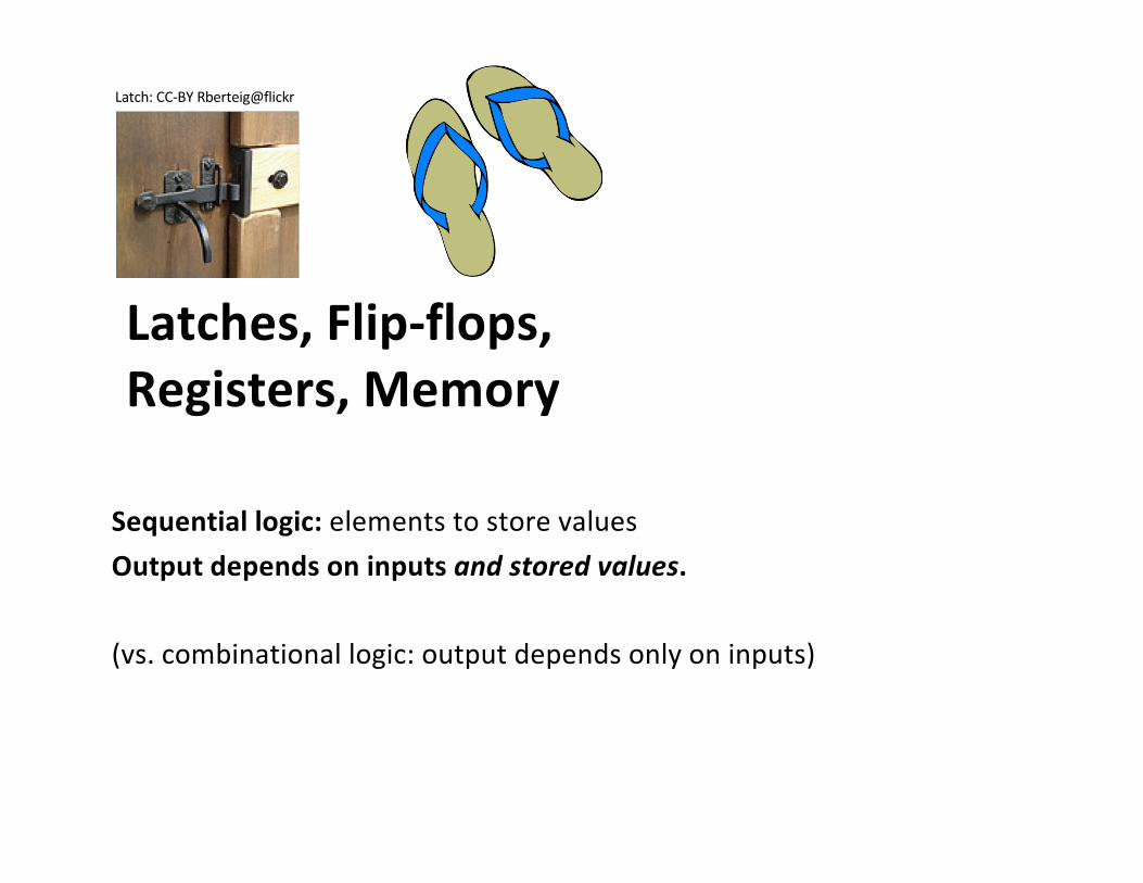
ALU
Processor: Data Path Components
Registers MemoryInstruction Fetch and Decode
12 3
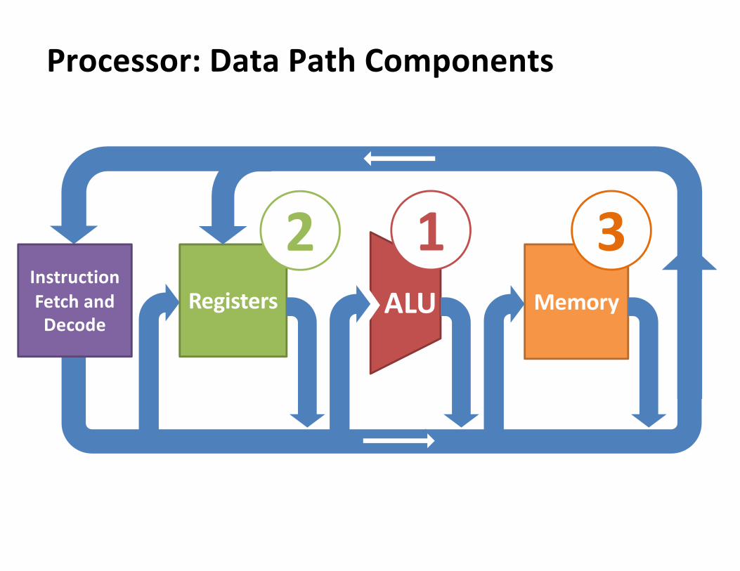
Bistable latches
Q Q
Suppose we somehow get a 1 (or a 0?) on here.
Q Q00
=
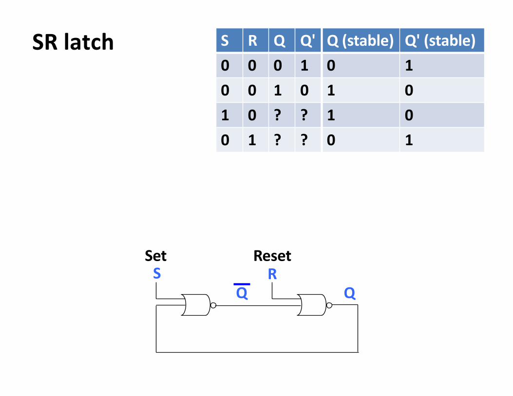
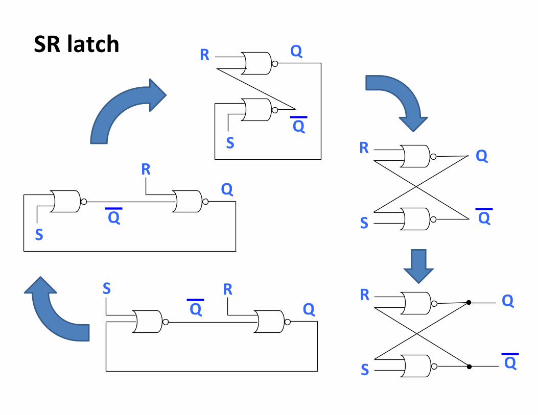
SR latch
Q QRS
Set Reset
S R Q Q' Q (stable) Q' (stable)0 0 0 1 0 10 0 1 0 1 01 0 ? ? 1 00 1 ? ? 0 1
SR latch
Q QRS
R
S
Q
QR
S R
S Q
Q
R
S Q
Q
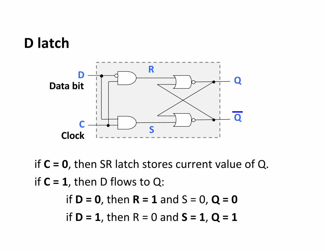
if C = 0, then SR latch stores current value of Q.if C = 1, then D flows to Q:
if D = 0, then R = 1 and S = 0, Q = 0if D = 1, then R = 0 and S = 1, Q = 1
D latch
D
C
R
S
Q
QClock
Data bit
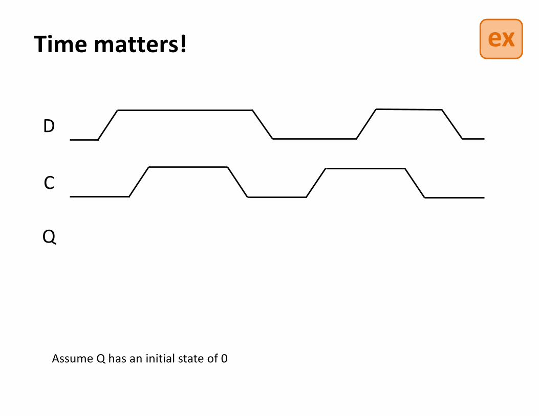
Time matters!
D
C
Q
Assume Q has an initial state of 0
ex
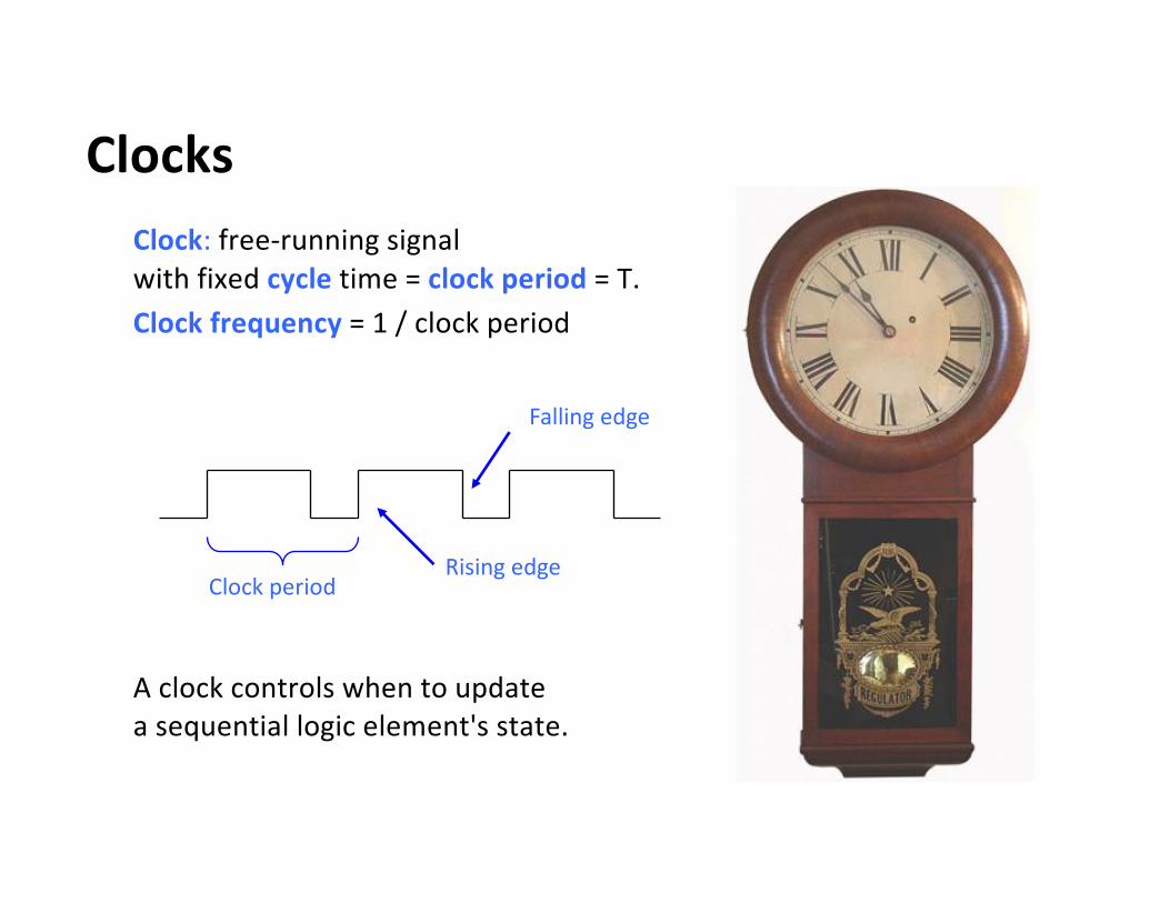
ClocksClock: free-running signalwith fixed cycle time = clock period = T. Clock frequency = 1 / clock period
A clock controls when to updatea sequential logic element's state.
Clock period
Falling edge
Rising edge
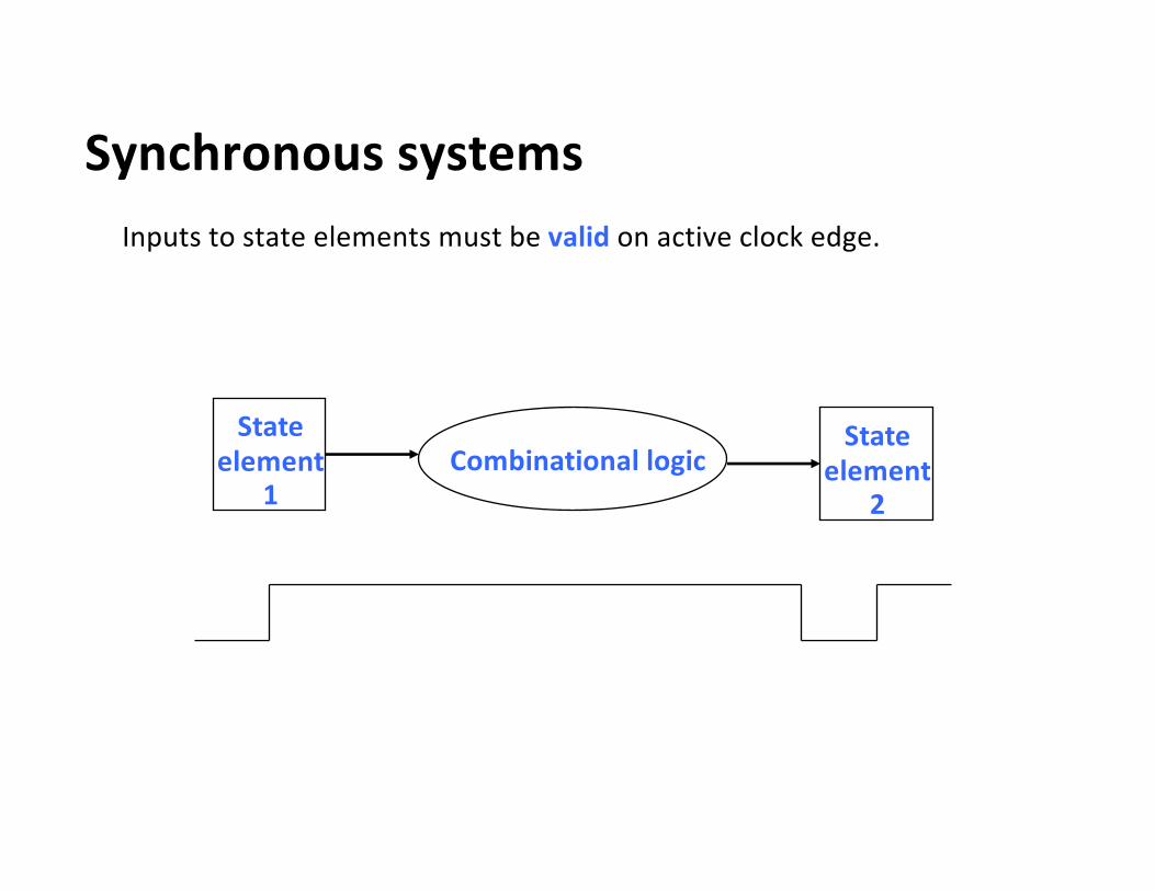
Synchronous systemsInputs to state elements must be valid on active clock edge.
Stateelement
1
Stateelement
2Combinational logic
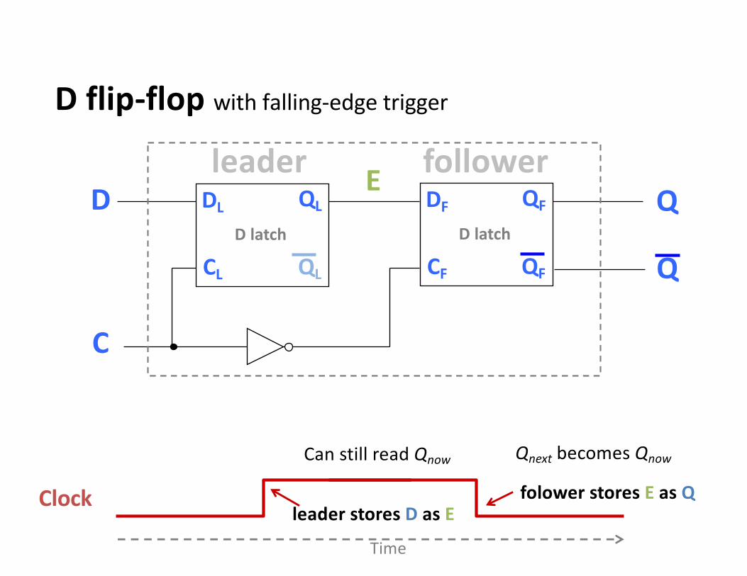
D flip-flop with falling-edge trigger
D
C
QEQLDL
CL
D latch
QL
QFDF
CF
D latch
QF Q
leader follower
Clockleader stores D as E
folower stores E as Q
Can still read Qnow Qnext becomes Qnow
Time
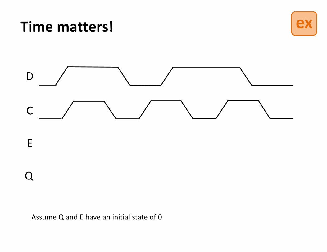
Time matters!
D
C
E
Q
Assume Q and E have an initial state of 0
ex
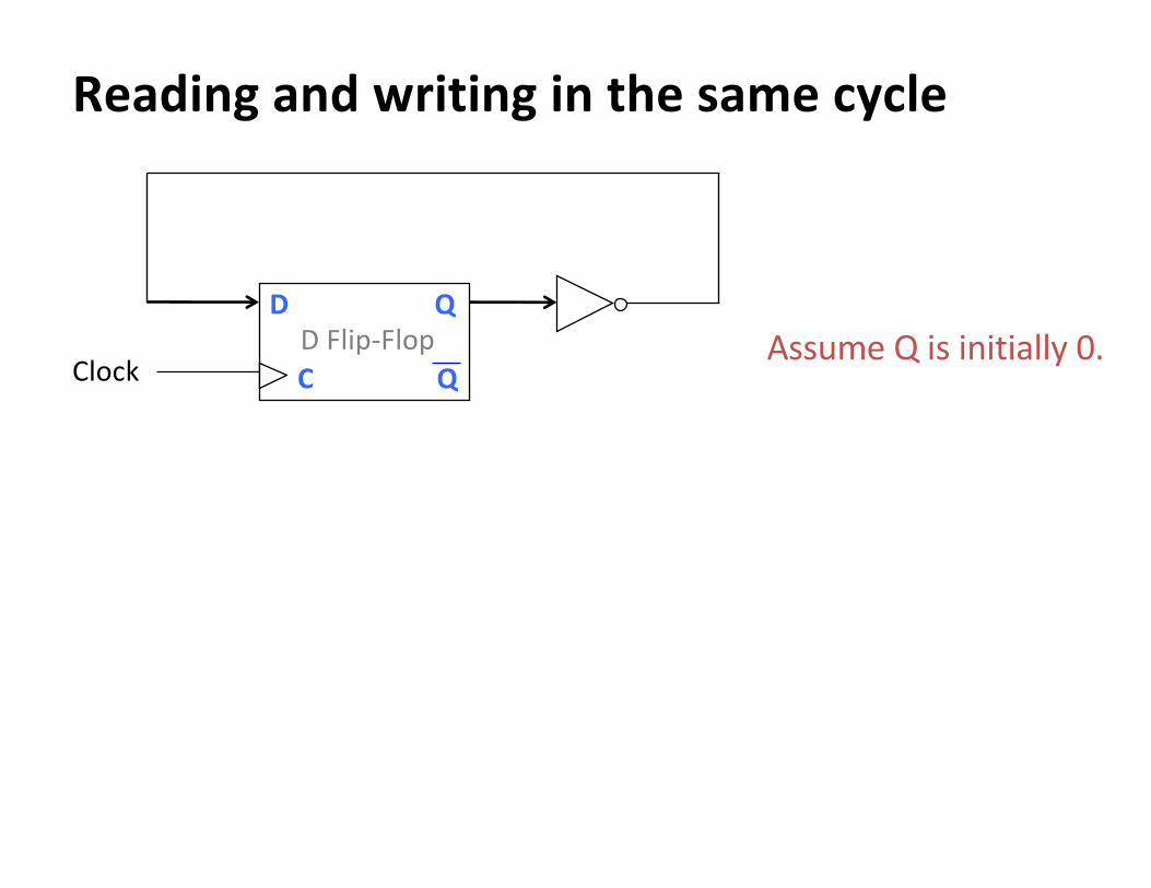
Reading and writing in the same cycle
Assume Q is initially 0.QD
CD Flip-Flop
QClock
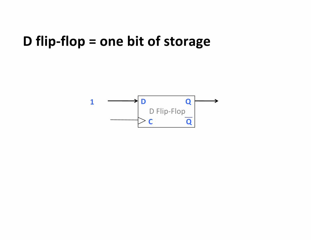
D flip-flop = one bit of storage
QD
CD Flip-Flop
Q
1
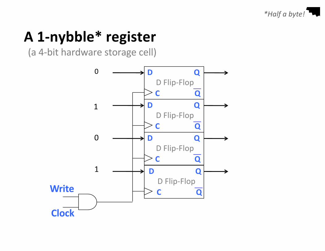
A 1-nybble* register(a 4-bit hardware storage cell)
Write
Clock
0
1
0
1
QD
CD Flip-Flop
QQD
CD Flip-Flop
QQD
CD Flip-Flop
QQD
CD Flip-Flop
Q
*Half a byte!
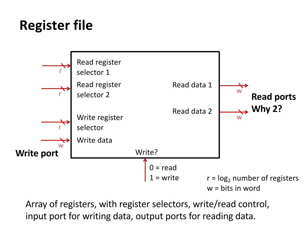
Register file
Read portsWhy 2?
Read registerselector 1Read registerselector 2
Write register selectorWrite data
Write?
Read data 1
Read data 2
r
r
r
w
w
w
r = log2 number of registersw = bits in word
Array of registers, with register selectors, write/read control,input port for writing data, output ports for reading data.
Write port0 = read1 = write
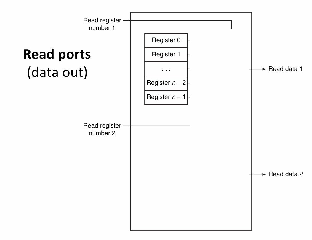
Read ports(data out)
C.8 Memory Elements: Flip-Flops, Latches, and Registers C-55
FIGURE C.8.7 A register fi le with two read ports and one write port has fi ve inputs and two outputs. The control input Write is shown in color.
FIGURE C.8.8 The implementation of two read ports for a register fi le with n registers can be done with a pair of n-to-1 multiplexors, each 32 bits wide. The register read number sig nal is used as the multiplexor selector signal. Figure C.8.9 shows how the write port is implemented.
Read registernumber 1 Read
data 1Read registernumber 2
Read data 2
Writeregister
WriteWritedata
Register file
Read registernumber 1
Register 0
Register 1
. . .
Register n – 2
Register n – 1
M
u
x
Read registernumber 2
M
u
x
Read data 1
Read data 2
AppendixC-9780123747501.indd 55AppendixC-9780123747501.indd 55 26/07/11 6:29 PM26/07/11 6:29 PM
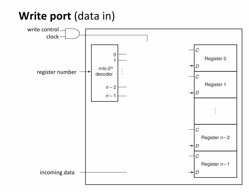
FIGURE C.8.9 The write port for a register fi le is implemented with a decoder that is used with the write signal to generate the C input to the registers. All three inputs (the regis ter number, the data, and the write signal) will have setup and hold-time constraints that ensure that the correct data is written into the register fi le.
Write
01
n-to-2n
decoder
n – 2
n – 1
Register 0
C
D
Register 1
C
D
Register n – 2
C
D
Register n – 1
C
D
...
Register number...
Register data
valid during the time it is read, as we saw earlier in Figure C.7.2. The value returned will be the value written in an earlier clock cycle. If we want a read to return the value currently being written, additional logic in the register fi le or out side of it is needed. Chapter 4 makes extensive use of such logic.
Specifying Sequential Logic in VerilogTo specify sequential logic in Verilog, we must understand how to generate a clock, how to describe when a value is written into a register, and how to specify sequential control. Let us start by specifying a clock. A clock is not a predefi ned object in Verilog; instead, we generate a clock by using the Verilog notation #n before a statement; this causes a delay of n simulation time steps before the execu tion of the statement. In most Verilog simulators, it is also possible to generate a clock as an external input, allowing the user to specify at simulation time the number of clock cycles during which to run a simulation.
The code in Figure C.8.10 implements a simple clock that is high or low for one simulation unit and then switches state. We use the delay capability and blocking assignment to implement the clock.
C-56 Appendix C The Basics of Logic Design
AppendixC-9780123747501.indd 56AppendixC-9780123747501.indd 56 26/07/11 6:29 PM26/07/11 6:29 PM
Write port (data in)
incoming data
register number
write controlclock
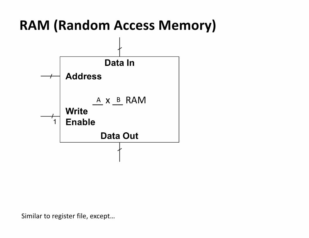
RAM (Random Access Memory)
Similar to register file, except…
A B
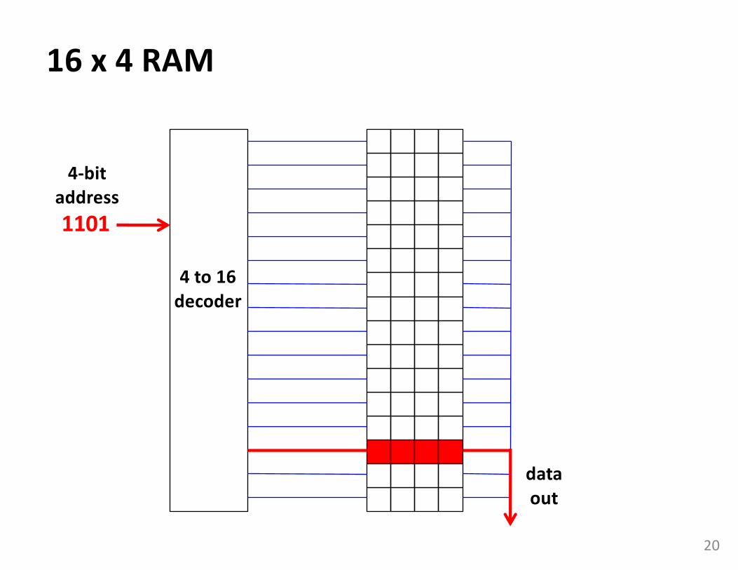
16 x 4 RAM
4 to 16decoder
dataout
1101
20
4-bitaddress