Combinational Logic Circuits PART2
34
Decoders • A decoder is a combinational circuit that converts binary information from n input lines to a maximum of 2 n unique output lines. If the n bit decoded information has unused or don’t care combinations, the decoder output will have fewer than 2 n outputs. • A decoder is a multiple-input, multiple- output logic circuit that converts coded inputs into coded outputs, where the input and output codes are different; e.g. n-to-2 n , BCD decoders. • Decoding is necessary in applications such as data multiplexing, 7 segment display and memory address decoding. Figure below shows the pseudo block of a decoder.
description
Logic Circuits
Transcript of Combinational Logic Circuits PART2
Decoders • A decoder is a combinational circuit that converts binary
information from n input lines to a maximum of 2n unique output lines. If the n bit decoded information has unused or don’t care combinations, the decoder output will have fewer than 2n outputs.
• A decoder is a multiple-input, multiple-output logic circuit that converts coded inputs into coded outputs, where the input and output codes are different; e.g. n-to-2n, BCD decoders.
• Decoding is necessary in applications such as data multiplexing, 7 segment display and memory address decoding. Figure below shows the pseudo block of a decoder.
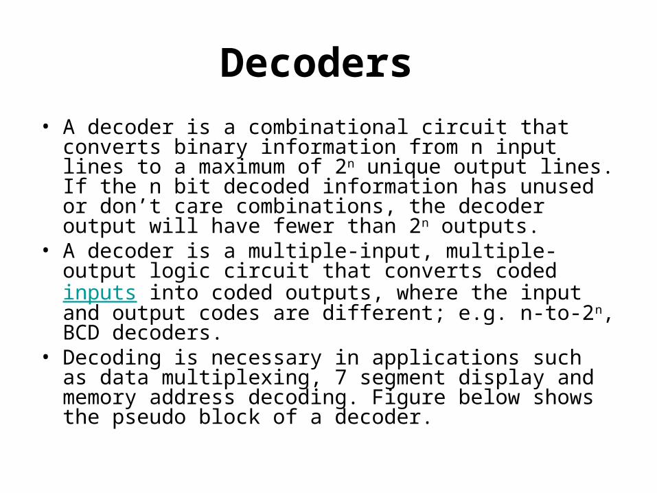
Basic Binary Decoder
• And AND gate can be used as the basic decoding element, because its output is HIGH only when all its inputs are HIGH. For example, if the input binary number is 0110, then, to make all the inputs to the AND gate HIGH, the two outer bits must be inverted using two inverters as shown in figure below.
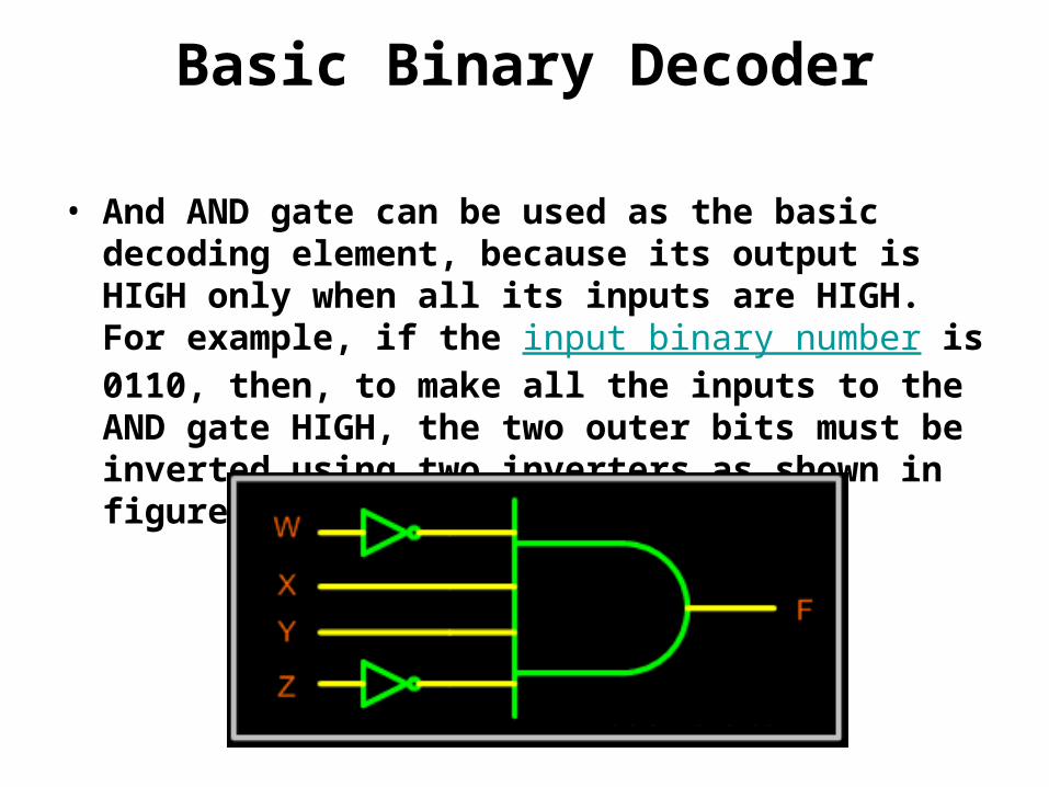
Binary n-to-2n Decoders • A binary decoder has n inputs and 2n
outputs. Only one output is active at any one time, corresponding to the input value. Figure below shows a representation of Binary n-to-2n decoder
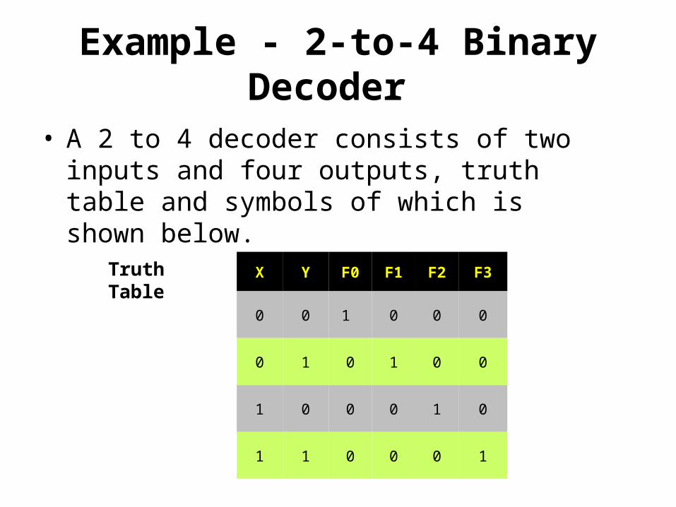
Example - 2-to-4 Binary Decoder
• A 2 to 4 decoder consists of two inputs and four outputs, truth table and symbols of which is shown below.
X Y F0 F1 F2 F3
0 0 1 0 0 0
0 1 0 1 0 0
1 0 0 0 1 0
1 1 0 0 0 1
Truth Table
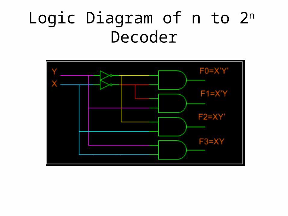
Logic Diagram of n to 2n Decoder

3-to-8 Binary Decoder • A 3 to 8 decoder consists of three inputs and
eight outputs, truth table and symbols of which is shown below.
X Y Z F0 F1 F2 F3 F4 F5 F6 F7
0 0 0 1 0 0 0 0 0 0 0
0 0 1 0 1 0 0 0 0 0 0
0 1 0 0 0 1 0 0 0 0 0
0 1 1 0 0 0 1 0 0 0 0
1 0 0 0 0 0 0 1 0 0 0
1 0 1 0 0 0 0 0 1 0 0
1 1 0 0 0 0 0 0 0 1 0
1 1 1 0 0 0 0 0 0 0 1
Truth Table

Block Diagram of 3 to 23 Decoder

Logic Diagram of 3 to 23
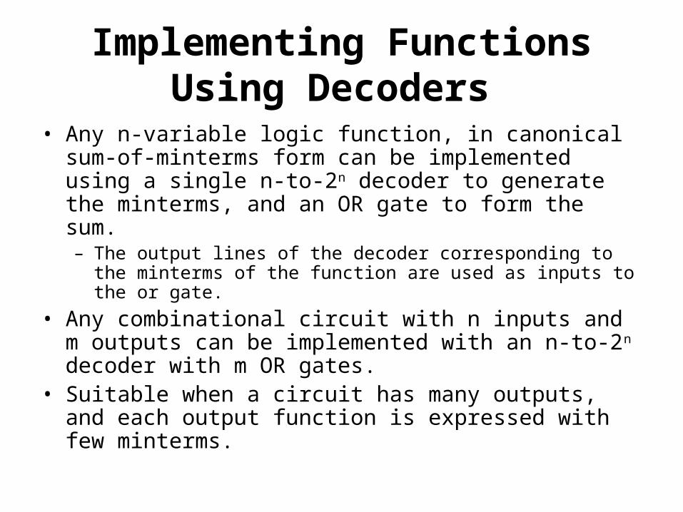
Implementing Functions Using Decoders
• Any n-variable logic function, in canonical sum-of-minterms form can be implemented using a single n-to-2n decoder to generate the minterms, and an OR gate to form the sum.– The output lines of the decoder corresponding to the minterms of
the function are used as inputs to the or gate.• Any combinational circuit with n inputs and m outputs
can be implemented with an n-to-2n decoder with m OR gates.
• Suitable when a circuit has many outputs, and each output function is expressed with few minterms.

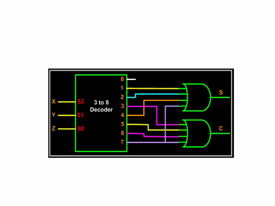
Example – Implement a Full adder using Decoder
X Y Z C S0 0 0 0 0
0 0 1 0 1
0 1 0 0 1
0 1 1 1 0
1 0 0 0 1
1 0 1 1 0
1 1 0 1 0
1 1 1 1 1
Truth Table
Equation S(x, y, z) = (1,2,4,7) C(x, y, z) = (3,5,6,7)
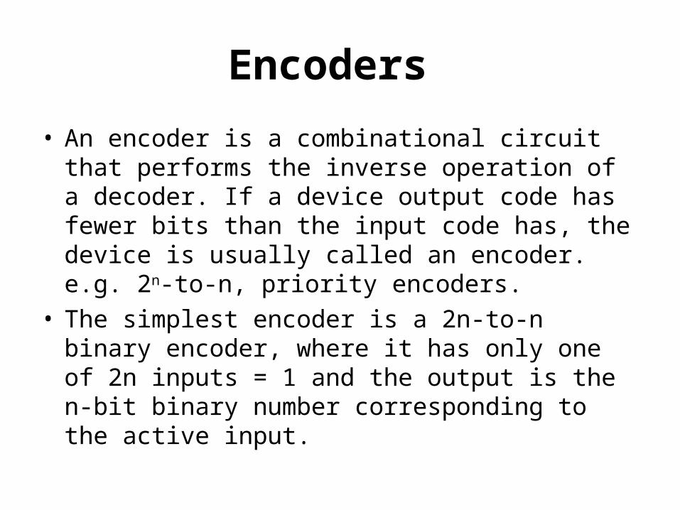
Encoders
• An encoder is a combinational circuit that performs the inverse operation of a decoder. If a device output code has fewer bits than the input code has, the device is usually called an encoder. e.g. 2n-to-n, priority encoders.
• The simplest encoder is a 2n-to-n binary encoder, where it has only one of 2n inputs = 1 and the output is the n-bit binary number corresponding to the active input.

Block Diagram
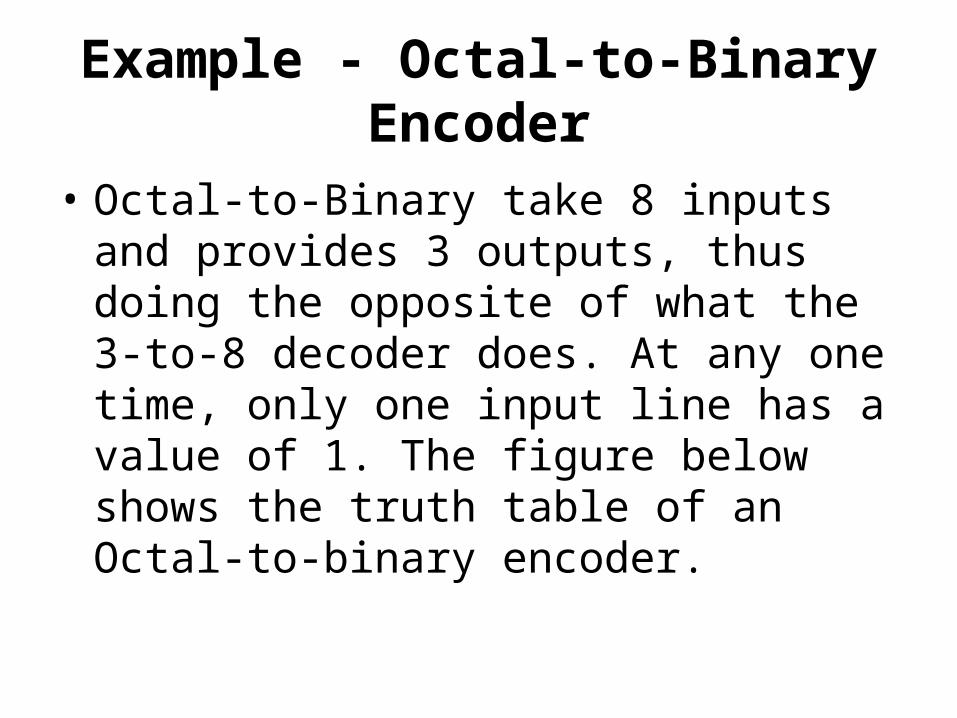
Example - Octal-to-Binary Encoder
• Octal-to-Binary take 8 inputs and provides 3 outputs, thus doing the opposite of what the 3-to-8 decoder does. At any one time, only one input line has a value of 1. The figure below shows the truth table of an Octal-to-binary encoder.

Truth TableI0 I1 I2 I3 I4 I5 I6 I7 Y2 Y1 Y0
1 0 0 0 0 0 0 0 0 0 0
0 1 0 0 0 0 0 0 0 0 1
0 0 1 0 0 0 0 0 0 1 0
0 0 0 1 0 0 0 0 0 1 1
0 0 0 0 1 0 0 0 1 0 0
0 0 0 0 0 1 0 0 1 0 1
0 0 0 0 0 0 1 0 1 1 0
0 0 0 0 0 0 0 1 1 1 1

• Y0 = I1 + I3 + I5 + I7 • Y1= I2 + I3 + I6 + I7
• Y2 = I4 + I5 + I6 +I7
Example - Decimal-to-Binary Encoder
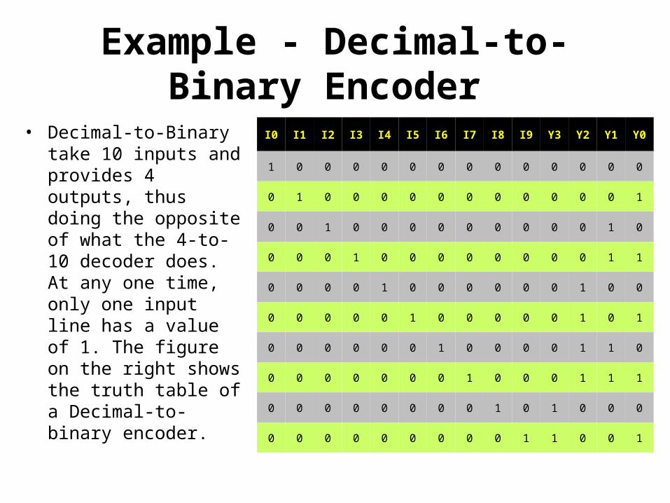
• Decimal-to-Binary take 10 inputs and provides 4 outputs, thus doing the opposite of what the 4-to-10 decoder does. At any one time, only one input line has a value of 1. The figure on the right shows the truth table of a Decimal-to-binary encoder.
I0 I1 I2 I3 I4 I5 I6 I7 I8 I9 Y3 Y2 Y1 Y0
1 0 0 0 0 0 0 0 0 0 0 0 0 0
0 1 0 0 0 0 0 0 0 0 0 0 0 1
0 0 1 0 0 0 0 0 0 0 0 0 1 0
0 0 0 1 0 0 0 0 0 0 0 0 1 1
0 0 0 0 1 0 0 0 0 0 0 1 0 0
0 0 0 0 0 1 0 0 0 0 0 1 0 1
0 0 0 0 0 0 1 0 0 0 0 1 1 0
0 0 0 0 0 0 0 1 0 0 0 1 1 1
0 0 0 0 0 0 0 0 1 0 1 0 0 0
0 0 0 0 0 0 0 0 0 1 1 0 0 1
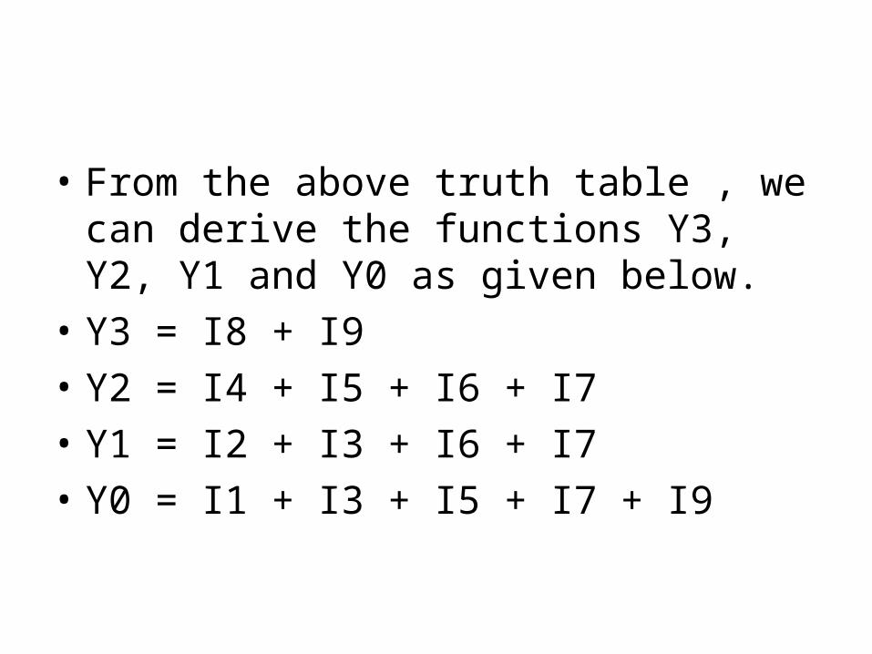
• From the above truth table , we can derive the functions Y3, Y2, Y1 and Y0 as given below.
• Y3 = I8 + I9 • Y2 = I4 + I5 + I6 + I7 • Y1 = I2 + I3 + I6 + I7 • Y0 = I1 + I3 + I5 + I7 + I9

Priority Encoder• If we look carefully at the Encoder circuits that we got,
we see the following limitations. If more than two inputs are active simultaneously, the output is unpredictable or rather it is not what we expect it to be.
• This ambiguity is resolved if priority is established so that only one input is encoded, no matter how many inputs are active at a given point of time.
• The priority encoder includes a priority function. The operation of the priority encoder is such that if two or more inputs are active at the same time, the input having the highest priority will take precedence.

Example – 4 to 3 Priority Encoder
• The truth table of a 4-input priority encoder is as shown below. The input D3 has the highest priority, D2 has next highest priority, D0 has the lowest priority. This means output Y2 and Y1 are 0 only when none of the inputs D1, D2, D3 are high and only D0 is high.
• A 4 to 3 encoder consists of four inputs and three outputs, truth table and symbols of which is shown below.

Truth Table
D3 D2 D1 D0 Y2 Y1 Y0
0 0 0 0 0 0 0
0 0 0 1 0 0 1
0 0 1 x 0 1 0
0 1 x x 0 1 1
1 x x x 1 0 0

Multiplexer
• Digital multiplexer is a combinational circuit that selects binary information from one of many input lines and directs it to a single output line. The selection of a particular input line is controlled by a set of selection lines.
• The block diagram of MUX with n data sources of b bits wide and s bits wide select line is shown in below figure.

Example of MUX

Mechanical Equivalent of a Multiplexer

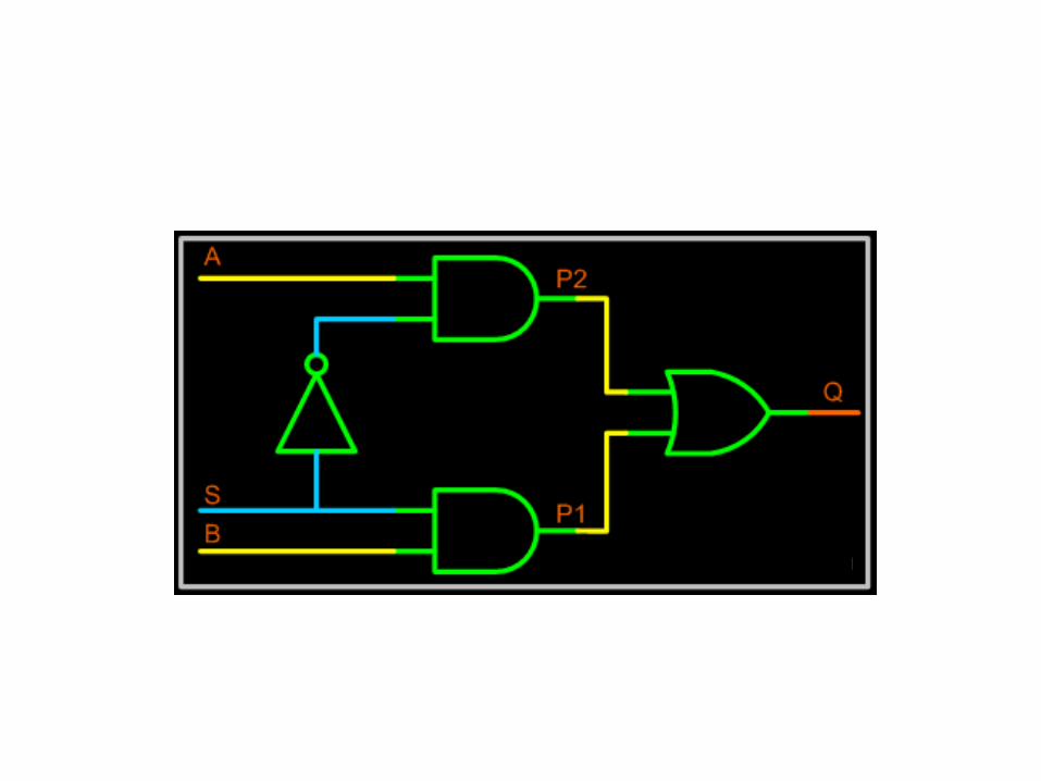
2 to 1 line multiplexer
S Y
0 A
1 B
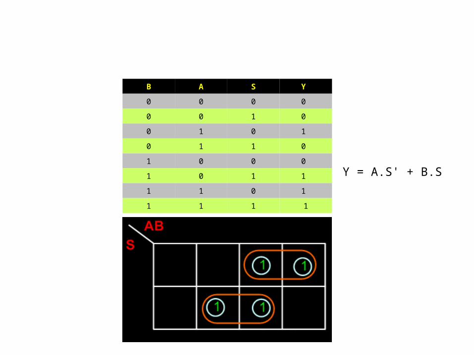
B A S Y
0 0 0 0
0 0 1 0
0 1 0 1
0 1 1 0
1 0 0 0
1 0 1 1
1 1 0 1
1 1 1 1
Y = A.S' + B.S

Example : 4:1 MUX
S1 S0 Y
0 0 I0
0 1 I1
1 0 I2
1 1 I3

Larger Multiplexers
• Larger multiplexers can be constructed from smaller ones. An 8-to-1 multiplexer can be constructed from smaller multiplexers as shown below.

Example - 8-to-1 multiplexer from Smaller MUX
S2 S1 S0 F
0 0 0 I0
0 0 1 I1
0 1 0 I2
0 1 1 I3
1 0 0 I4
1 0 1 I5
1 1 0 I6
1 1 1 I7

Example - 16-to-1 multiplexer from 4:1 mux

Exercises
1. Construct a 16 bit parallel adder with four MSI circuits, each containing a 4-bit parallel adder. Use block diagram with nine inputs and five outputs for each 4-bit adder. Show how carries are connected between the MSI circuits.
2. Construct a 5 X 32 decoder with four 3 X 8 decoders with enable and 0ne 2 X 4 decoder. Use block diagram.

3. Implement the following Boolean function with an 8 X 1 multiplexer. F(A,B,C,D) =∑(0,3,5,6,8,9,14,15).

References:– Digital Design 2nd Edition, M. Morris Mano– Digital Design, M. Morris Mano– Digital Design Principles and Practices 3rd Edition,
John F. Wakerly– Digital Systems Principles and Application 6th
Edition by Tocci– WEBSITEShttp://www.asic-world.com/digitalhttp://www.youtube.com/watch?
v=NrpW1e8IFeA&feature=related