Combinational-Circuit Building Blocks Data Flow Modeling of Combinational Logic
Upload
andra-robbinsCategory
view
214download
0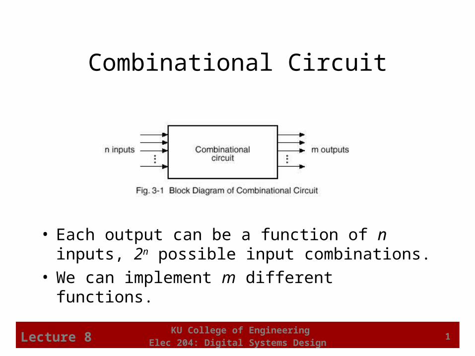
KU College of EngineeringElec 204: Digital Systems DesignLecture 8 1
Combinational Circuit
• Each output can be a function of n inputs, 2n possible input combinations.
• We can implement m different functions.
KU College of EngineeringElec 204: Digital Systems DesignLecture 8 2
Design Schemes
• VLSI circuit: millions of gates– Not manageable
– Need to divide sub-circuits
• Divide-and-Conquer Approach– Hierarchical Design
• Broke circuits into pieces of blocks
• Each block has a certain I/O
KU College of EngineeringElec 204: Digital Systems DesignLecture 8 3
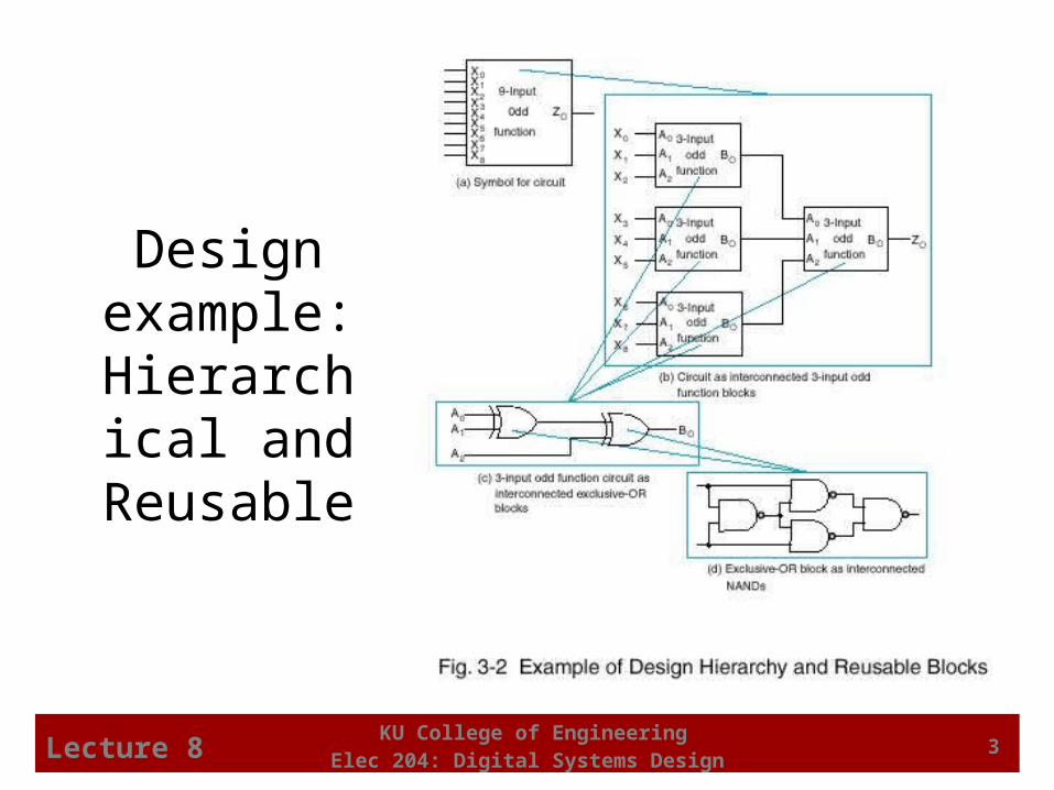
Design example:
Hierarchical and
Reusable
KU College of EngineeringElec 204: Digital Systems DesignLecture 8 4
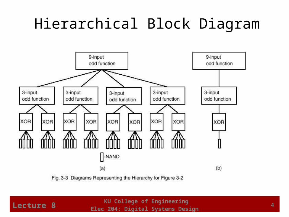
Hierarchical Block Diagram
KU College of EngineeringElec 204: Digital Systems DesignLecture 8 5
Top-Down versus Bottom-Up
• A top-down design proceeds from an abstract, high-level specification to a more and more detailed design by decomposition and successive refinement
• A bottom-up design starts with detailed primitive blocks and combines them into larger and more complex functional blocks
• Designs usually proceed from both directions simultaneously
– Top-down design answers: What are we building?
– Bottom-up design answers: How do we build it?
• Top-down controls complexity while bottom-up focuses on the details
KU College of EngineeringElec 204: Digital Systems DesignLecture 8 6
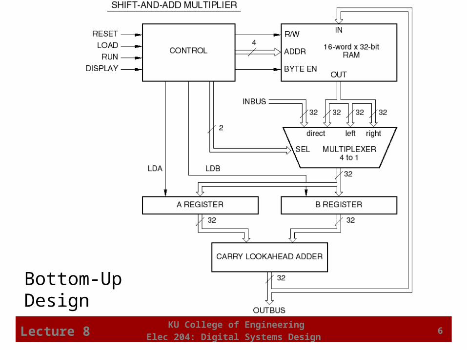
Bottom-Up Design
KU College of EngineeringElec 204: Digital Systems DesignLecture 8 7
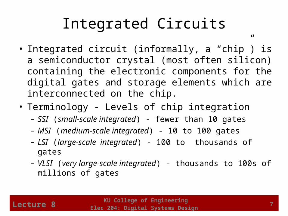
Integrated Circuits
• Integrated circuit (informally, a “chip”) is a semiconductor crystal (most often silicon) containing the electronic components for the digital gates and storage elements which are interconnected on the chip.
• Terminology - Levels of chip integration– SSI (small-scale integrated) - fewer than 10 gates
– MSI (medium-scale integrated) - 10 to 100 gates
– LSI (large-scale integrated) - 100 to thousands of gates
– VLSI (very large-scale integrated) - thousands to 100s of millions of gates

KU College of EngineeringElec 204: Digital Systems DesignLecture 8 8
Technology Parameters• Specific gate implementation technologies are characterized
by the following parameters: – Fan-in – the number of inputs available on a gate– Fan-out – the number of standard loads driven by a gate output– Logic Levels – the signal value ranges for 1 and 0 on the inputs and 1
and 0 on the outputs– Noise Margin – the maximum external noise voltage superimposed on
a normal input value that will not cause an undesirable change in the circuit output
– Cost for a gate - a measure of the contribution by the gate to the cost of the integrated circuit
– Propagation Delay – The time required for a change in the value of a signal to propagate from an input to an output
– Power Dissipation – the amount of power drawn from the power supply and consumed by the gate
KU College of EngineeringElec 204: Digital Systems DesignLecture 8 9
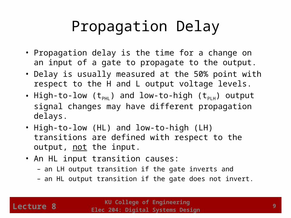
Propagation Delay
• Propagation delay is the time for a change on an input of a gate to propagate to the output.
• Delay is usually measured at the 50% point with respect to the H and L output voltage levels.
• High-to-low (tPHL) and low-to-high (tPLH) output signal changes may have different propagation delays.
• High-to-low (HL) and low-to-high (LH) transitions are defined with respect to the output, not the input.
• An HL input transition causes:– an LH output transition if the gate inverts and
– an HL output transition if the gate does not invert.
KU College of EngineeringElec 204: Digital Systems DesignLecture 8 10
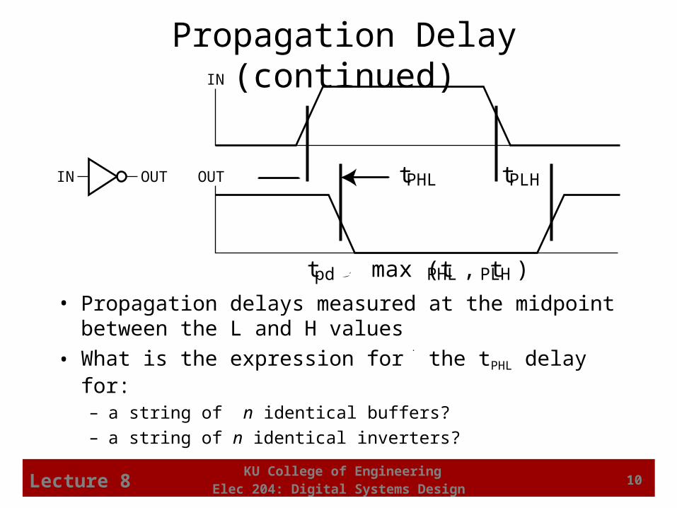
Propagation Delay (continued)
• Propagation delays measured at the midpoint between the L and H values
• What is the expression for the tPHL delay for:– a string of n identical buffers?
– a string of n identical inverters?
IN
OUT tPHL tPLH
tpd5 max (tPHL , tPLH )
IN OUT
KU College of EngineeringElec 204: Digital Systems DesignLecture 8 11
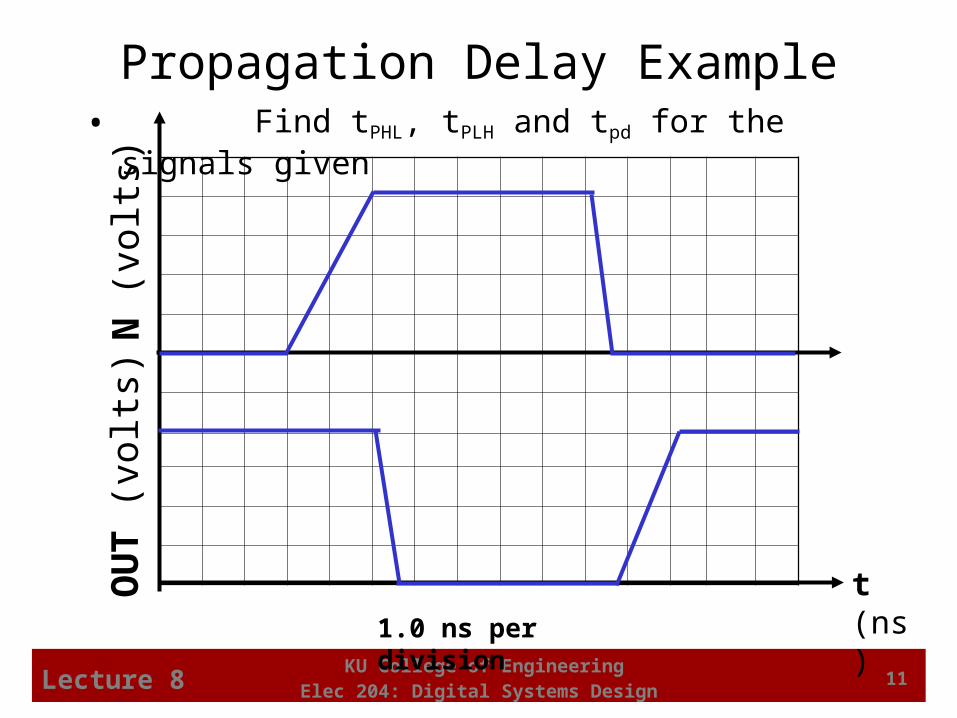
Propagation Delay Example• Find tPHL, tPLH and tpd for the signals given
IN (
volt
s)O
UT
(vo
lts)
t (ns)1.0 ns per division
KU College of EngineeringElec 204: Digital Systems DesignLecture 8 12
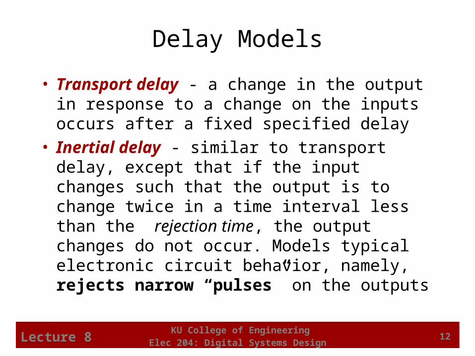
Delay Models
• Transport delay - a change in the output in response to a change on the inputs occurs after a fixed specified delay
• Inertial delay - similar to transport delay, except that if the input changes such that the output is to change twice in a time interval less than the rejection time, the output changes do not occur. Models typical electronic circuit behavior, namely, rejects narrow “pulses” on the outputs
KU College of EngineeringElec 204: Digital Systems DesignLecture 8 13
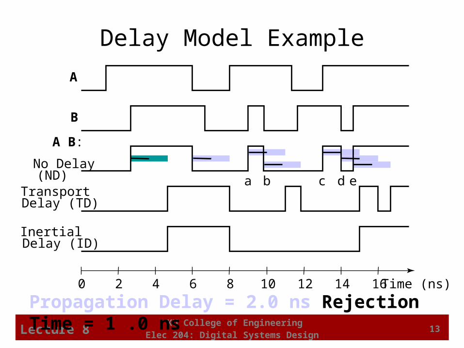
Delay Model Example
A
A B:
TransportDelay (TD)
InertialDelay (ID)
B
Time (ns)0 42 6 8 10 12 14 16
No Delay(ND) a b c d e
Propagation Delay = 2.0 ns Rejection Time = 1 .0 ns
KU College of EngineeringElec 204: Digital Systems DesignLecture 8 14
Fan-out
• Fan-out can be defined in terms of a standard load– Example: 1 standard load equals the load
contributed by the input of 1 inverter.– Transition time -the time required for the gate
output to change from H to L, tHL, or from L to H, tLH
– The maximum fan-out that can be driven by a gate is the number of standard loads the gate can drive without exceeding its specified maximum transition time
KU College of EngineeringElec 204: Digital Systems DesignLecture 8 15
Fan-out and Delay
• The fan-out loading of a gate’s output affects the gate’s propagation delay
• Example:– One realistic equation for tpd for a NAND gate
with 4 inputs is:
tpd = 0.07 + 0.021 SL ns
– SL is the number of standard loads the gate is driving, i. e., its fan-out in standard loads
– For SL = 4.5, tpd = 0.165 ns
KU College of EngineeringElec 204: Digital Systems DesignLecture 8 16
Cost• In an integrated circuit:
– The cost of a gate is proportional to the chip area occupied by the gate
– The gate area is roughly proportional to the number and size of the transistors and the amount of wiring connecting them
– Ignoring the wiring area, the gate area is roughly proportional to the gate input count
– So gate input count is a rough measure of gate cost
• If the actual chip layout area occupied by the gate is known, it is a far more accurate measure

KU College of EngineeringElec 204: Digital Systems DesignLecture 8 17
Design Procedure1. Specification
– Write a specification for the circuit if one is not already available
2. Formulation– Derive a truth table or initial Boolean equations that define the
required relationships between the inputs and outputs, if not in the specification
3. Optimization– Apply 2-level and multiple-level optimization– Draw a logic diagram or provide a netlist for the resulting circuit
using ANDs, ORs, and inverters
4. Technology Mapping– Map the logic diagram or netlist to the implementation technology
selected
5. Verification– Verify the correctness of the final design

KU College of EngineeringElec 204: Digital Systems DesignLecture 8 18
Design Example
1. Specification – BCD to Excess-3 code converter– Transforms BCD code for the decimal digits to Excess-3
code for the decimal digits– BCD code words for digits 0 through 9: 4-bit patterns 0000
to 1001, respectively– Excess-3 code words for digits 0 through 9: 4-bit patterns
consisting of 3 (binary 0011) added to each BCD code word
– Implementation: • multiple-level circuit• NAND gates (including inverters)
KU College of EngineeringElec 204: Digital Systems DesignLecture 8 19
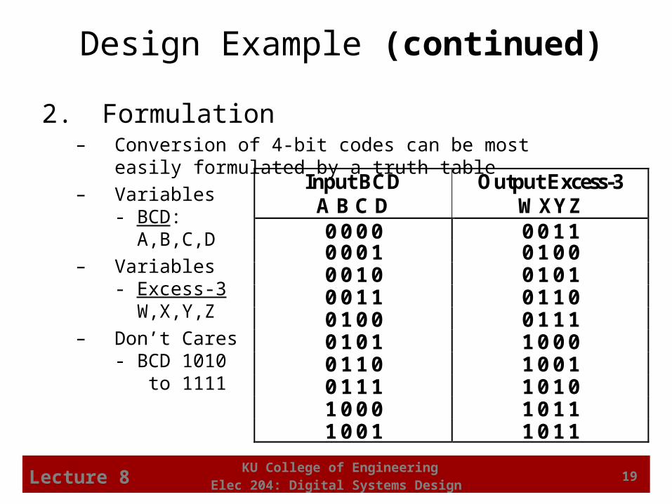
Design Example (continued)
2. Formulation– Conversion of 4-bit codes can be most easily formulated by a
truth table
– Variables- BCD: A,B,C,D
– Variables- Excess-3 W,X,Y,Z
– Don’t Cares- BCD 1010 to 1111
Input BCD A B C D
Output Excess-3 WXYZ
0 0 0 0 0 0 1 1 0 0 0 1 0 1 0 0 0 0 1 0 0 1 0 1 0 0 1 1 0 1 1 0 0 1 0 0 0 1 1 1 0 1 0 1 1 0 0 0 0 1 1 0 1 0 0 1 0 1 1 1 1 0 1 0 1 0 0 0 1 0 1 1 1 0 0 1 1 0 1 1
KU College of EngineeringElec 204: Digital Systems DesignLecture 8 20
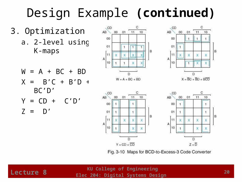
Design Example (continued)
3. Optimizationa. 2-level using
K-maps
W = A + BC + BD
X = B’C + B’D + BC’D’
Y = CD + C’D’
Z = D’
KU College of EngineeringElec 204: Digital Systems DesignLecture 8 21
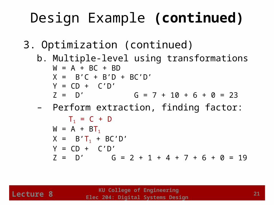
Design Example (continued)
3. Optimization (continued)b. Multiple-level using transformations
W = A + BC + BDX = B’C + B’D + BC’D’Y = CD + C’D’Z = D’ G = 7 + 10 + 6 + 0 = 23
– Perform extraction, finding factor: T1 = C + D
W = A + BT1 X = B’T1 + BC’D’Y = CD + C’D’Z = D’ G = 2 + 1 + 4 + 7 + 6 + 0 = 19
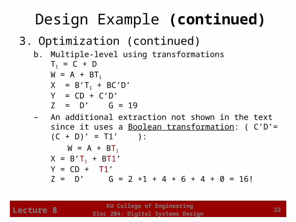
KU College of EngineeringElec 204: Digital Systems DesignLecture 8 22
Design Example (continued)
3. Optimization (continued)b. Multiple-level using transformations
T1 = C + DW = A + BT1 X = B’T1 + BC’D’Y = CD + C’D’ Z = D’ G = 19
– An additional extraction not shown in the text since it uses a Boolean transformation: ( C’D’= (C + D)’ = T1’ ):
W = A + BT1
X = B’T1 + BT1’ Y = CD + T1’Z = D’ G = 2 +1 + 4 + 6 + 4 + 0 = 16!
KU College of EngineeringElec 204: Digital Systems DesignLecture 8 23
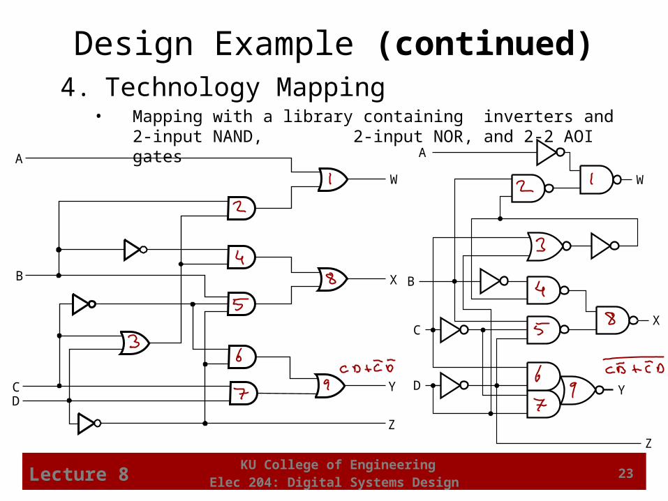
Design Example (continued)4. Technology Mapping
• Mapping with a library containing inverters and 2-input NAND, 2-input NOR, and 2-2 AOI gates
A
B
C
D
W
X
Y
Z
A
B
CD
W
X
Y
Z
KU College of EngineeringElec 204: Digital Systems DesignLecture 8 24
Technology Mapping
• Chip design styles• Cells and cell libraries• Mapping Techniques
– NAND gates
– NOR gates
– Multiple gate types
– Programmable logic devices
KU College of EngineeringElec 204: Digital Systems DesignLecture 8 25
Chip Design Styles• Full custom - the entire design of the chip down to the smallest detail
of the layout is performed– Expensive
– Justifiable only for dense, fast chips with high sales volume
• Standard cell - blocks have been design ahead of time or as part of previous designs– Intermediate cost
– Less density and speed compared to full custom
• Gate array - regular patterns of gate transistors that can be used in many designs built into chip - only the interconnections between gates are specific to a design– Lowest cost
– Less density compared to full custom and standard cell
KU College of EngineeringElec 204: Digital Systems DesignLecture 8 26
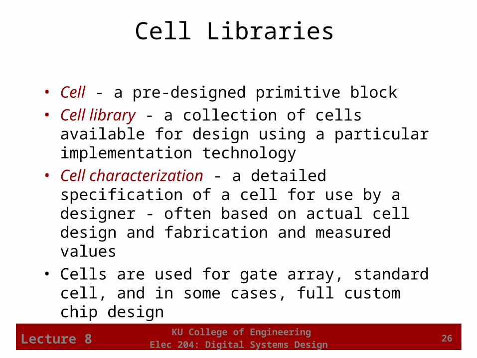
Cell Libraries
• Cell - a pre-designed primitive block
• Cell library - a collection of cells available for design using a particular implementation technology
• Cell characterization - a detailed specification of a cell for use by a designer - often based on actual cell design and fabrication and measured values
• Cells are used for gate array, standard cell, and in some cases, full custom chip design
KU College of EngineeringElec 204: Digital Systems DesignLecture 8 27
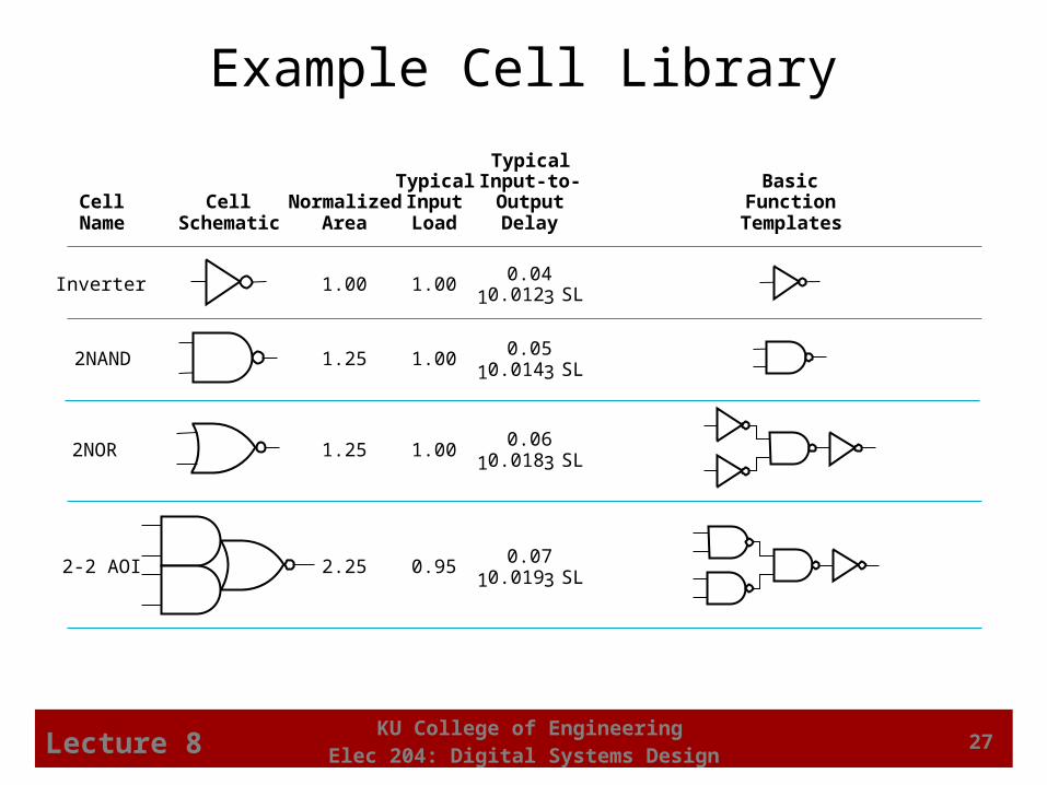
Example Cell Library
CellName
CellSchematic
NormalizedArea
TypicalInputLoad
TypicalInput-to-OutputDelay
BasicFunction
Templates
Inverter 1.00 1.00 0.0410.0123 SL
2NAND 1.25 1.00 0.0510.0143 SL
2NOR 1.25 1.00 0.0610.0183 SL
2-2 AOI 2.25 0.95 0.0710.0193 SL

KU College of EngineeringElec 204: Digital Systems DesignLecture 8 28
• Verification - show that the final circuit designed implements the original specification
• Simple specifications are:– truth tables
– Boolean equations
– HDL code
• If the above result from formulation are not the original specification, it is critical that the formulation process be flawless for the verification to be valid!
Verification
KU College of EngineeringElec 204: Digital Systems DesignLecture 8 29
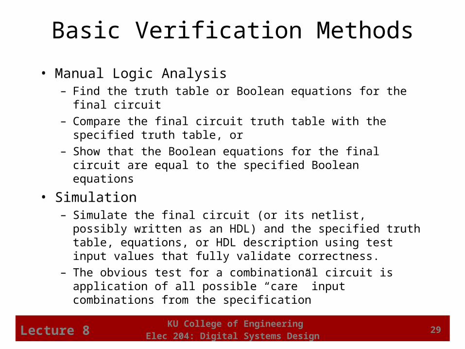
Basic Verification Methods
• Manual Logic Analysis– Find the truth table or Boolean equations for the final circuit
– Compare the final circuit truth table with the specified truth table, or
– Show that the Boolean equations for the final circuit are equal to the specified Boolean equations
• Simulation– Simulate the final circuit (or its netlist, possibly written as an
HDL) and the specified truth table, equations, or HDL description using test input values that fully validate correctness.
– The obvious test for a combinational circuit is application of all possible “care” input combinations from the specification

KU College of EngineeringElec 204: Digital Systems DesignLecture 8 30
Programmable Implementation Technologies
• Why programmable logic?• Programmable logic technologies• Read-Only Memory (ROM)• Programmable Logic Array (PLA)• Programmable Array Logic (PAL)
KU College of EngineeringElec 204: Digital Systems DesignLecture 8 31
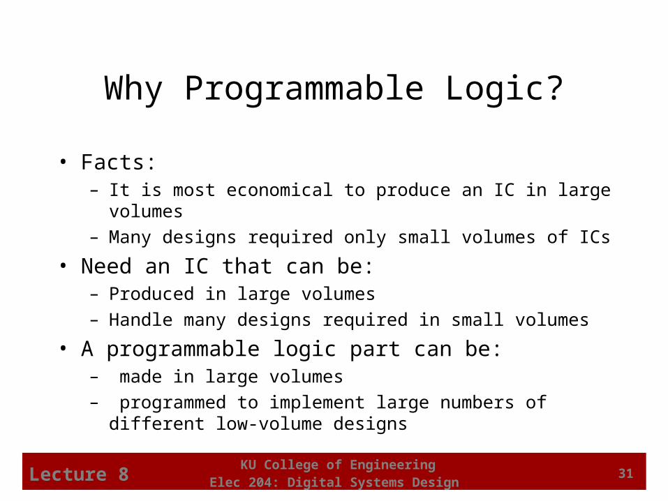
Why Programmable Logic?
• Facts:– It is most economical to produce an IC in large volumes
– Many designs required only small volumes of ICs
• Need an IC that can be:– Produced in large volumes
– Handle many designs required in small volumes
• A programmable logic part can be:– made in large volumes
– programmed to implement large numbers of different low-volume designs
KU College of EngineeringElec 204: Digital Systems DesignLecture 8 32
Programmable Logic - Additional Advantages
• Many programmable logic devices are field- programmable, i.e., can be programmed outside of the manufacturing environment
• Most programmable logic devices are erasable and reprogrammable.– Allows “updating” a device or correction of errors
– Allows reuse the device for a different design - the ultimate in re-usability!
– Ideal for course laboratories
• Programmable logic devices can be used to prototype design that will be implemented for sale in regular ICs.– Complete Intel Pentium designs were actually prototype with
specialized systems based on large numbers of VLSI programmable devices!
KU College of EngineeringElec 204: Digital Systems DesignLecture 8 33
Programming Technologies
• Programming technologies are used to:– Control connections
– Build lookup tables
– Control transistor switching
• The technologies– Control connections
• Mask programming
• Fuse
• Antifuse
• Single-bit storage element
KU College of EngineeringElec 204: Digital Systems DesignLecture 8 34
Programming Technologies
• The technologies (continued)– Build lookup tables
• Storage elements (as in a memory)
– Transistor Switching Control • Stored charge on a floating transistor gate
– Erasable
– Electrically erasable
– Flash (as in Flash Memory)
• Storage elements (as in a memory)

KU College of EngineeringElec 204: Digital Systems DesignLecture 8 35
Technology Characteristics
• Permanent - Cannot be erased and reprogrammed
• Mask programming
• Fuse
• Antifuse
• Reprogrammable– Volatile - Programming lost if chip power lost
• Single-bit storage element
– Non-Volatile• Erasable
• Electrically erasable
• Flash (as in Flash Memory)

KU College of EngineeringElec 204: Digital Systems DesignLecture 8 36
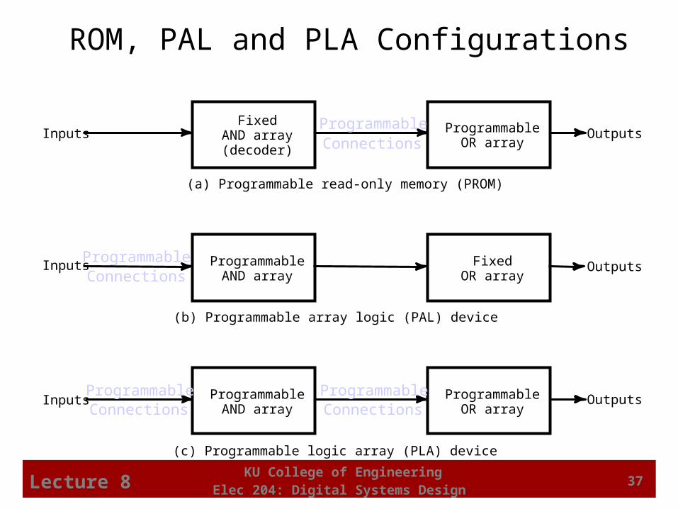
Programmable Configurations
• Read Only Memory (ROM) – – a fixed array of AND gates and a programmable array of OR gates
• Programmable Array Logic (PAL) – – a programmable array of AND gates feeding a fixed array of OR
gates.
• Programmable Logic Array (PLA) –– a programmable array of AND gates feeding a programmable array
of OR gates.
• Complex Programmable Logic Device (CPLD) /Field- Programmable Gate Array (FPGA) – – complex enough to be called “architectures”
KU College of EngineeringElec 204: Digital Systems DesignLecture 8 37
ROM, PAL and PLA Configurations
(a) Programmable read-only memory (PROM)
InputsFixed
AND array(decoder)
ProgrammableOR array
OutputsProgrammableConnections
(b) Programmable array logic (PAL) device
Inputs ProgrammableAND array
FixedOR array
OutputsProgrammableConnections
(c) Programmable logic array (PLA) device
Inputs ProgrammableOR array
OutputsProgrammableConnections
ProgrammableConnections
ProgrammableAND array
KU College of EngineeringElec 204: Digital Systems DesignLecture 8 38
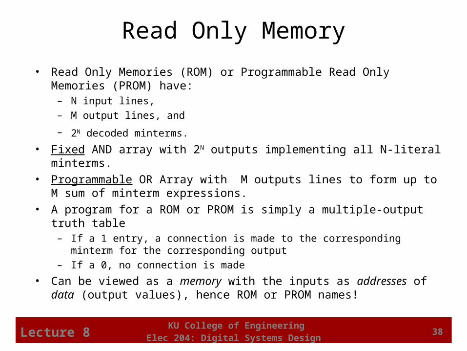
Read Only Memory
• Read Only Memories (ROM) or Programmable Read Only Memories (PROM) have:
– N input lines,
– M output lines, and
– 2N decoded minterms. • Fixed AND array with 2N outputs implementing all N-literal minterms.
• Programmable OR Array with M outputs lines to form up to M sum of minterm expressions.
• A program for a ROM or PROM is simply a multiple-output truth table– If a 1 entry, a connection is made to the corresponding minterm for the corresponding
output
– If a 0, no connection is made
• Can be viewed as a memory with the inputs as addresses of data (output values), hence ROM or PROM names!
KU College of EngineeringElec 204: Digital Systems DesignLecture 8 39
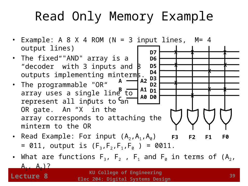
• Example: A 8 X 4 ROM (N = 3 input lines, M= 4 output lines)
• The fixed "AND" array is a“decoder” with 3 inputs and 8outputs implementing minterms.
• The programmable "OR“array uses a single line torepresent all inputs to anOR gate. An “X” in thearray corresponds to attaching theminterm to the OR
• Read Example: For input (A2,A1,A0)= 011, output is (F3,F2,F1,F0 ) = 0011.
• What are functions F3, F2 , F1 and F0 in terms of (A2, A1, A0)?
Read Only Memory Example
D7D6D5D4D3D2D1D0
A2
A1A0
A
B
C
F0F1F2F3
X XX
XX
X
XX
XX
KU College of EngineeringElec 204: Digital Systems DesignLecture 8 40
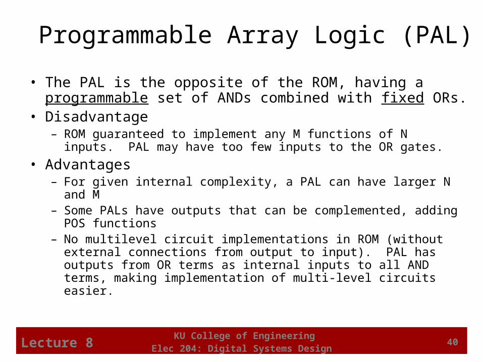
Programmable Array Logic (PAL)
• The PAL is the opposite of the ROM, having a programmable set of ANDs combined with fixed ORs.
• Disadvantage– ROM guaranteed to implement any M functions of N
inputs. PAL may have too few inputs to the OR gates.
• Advantages– For given internal complexity, a PAL can have larger N and M– Some PALs have outputs that can be complemented, adding POS
functions– No multilevel circuit implementations in ROM (without external
connections from output to input). PAL hasoutputs from OR terms as internal inputs to all ANDterms, making implementation of multi-level circuits easier.
KU College of EngineeringElec 204: Digital Systems DesignLecture 8 41
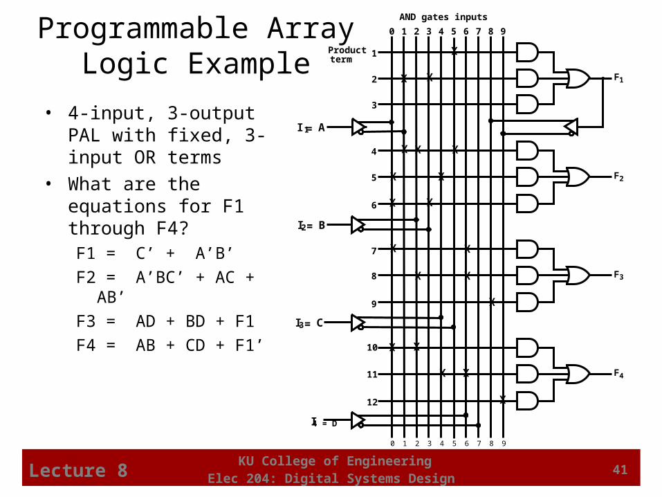
Programmable Array Logic Example
• 4-input, 3-output PAL with fixed, 3-input OR terms
• What are the equations for F1 through F4?F1 = C’ + A’B’
F2 = A’BC’ + AC + AB’
F3 = AD + BD + F1
F4 = AB + CD + F1’
0 91 2 3 4 5 6 7 8
AND gates inputs
0 9
Productterm
1
2
3
4
5
6
7
8
9
10
11
12
F1
F2
F3
F4
I3= C
I2= B
I 1= A
1 2 3 4 5 6 7 8
I4 = D
X X
X X
X X X
X X
X
X
X
XX
X
X X
X
X X
KU College of EngineeringElec 204: Digital Systems DesignLecture 8 42
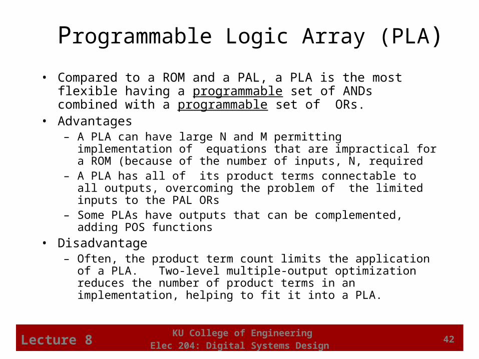
Programmable Logic Array (PLA)
• Compared to a ROM and a PAL, a PLA is the most flexible having a programmable set of ANDs combined with a programmable set of ORs.
• Advantages– A PLA can have large N and M permitting implementation of equations
that are impractical for a ROM (because of the number of inputs, N, required
– A PLA has all of its product terms connectable to all outputs, overcoming the problem of the limited inputs to the PAL ORs
– Some PLAs have outputs that can be complemented, adding POS functions
• Disadvantage– Often, the product term count limits the application of a PLA. Two-level
multiple-output optimization reduces the number of product terms in an implementation, helping to fit it into a PLA.
KU College of EngineeringElec 204: Digital Systems DesignLecture 8 43
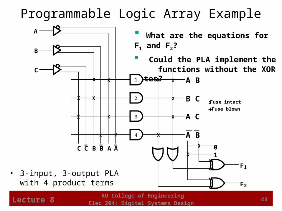
Programmable Logic Array Example
• 3-input, 3-output PLA with 4 product terms
What are the equations for F1 and F2?
Could the PLA implement the functions without the XOR gates?
Fuse intact
Fuse blown
1
F1
F2
X
A
B
C
C C B B A A 0
1
2
3
4X
XX
X X
X
X
X
X
X
X
X
X
X A B
A C
B C
A B
X