ELEC 1041 OR gate with inverted inputs is a NAND …nseng.tripod.com/elec1041/lec02-color.pdf ·...
9
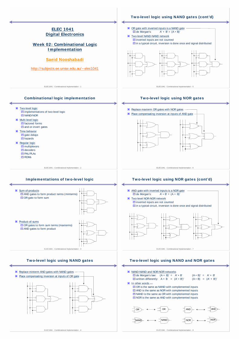
ELEC1041 - Combinational Implementation - 1 ELEC 1041 Digital Electronics Week 02: Combinational Logic Implementation Saeid Nooshabadi http://subjects. ee . unsw . edu .au/~elec1041 ELEC1041 - Combinational Implementation - 2 Combinational logic implementation ! Two-level logic " implementations of two-level logic " NAND/NOR ! Multi-level logic " factored forms " and-or-invert gates ! Time behavior " gate delays " hazards ! Regular logic " multiplexors " decoders " PAL/PLAs " ROMs ELEC1041 - Combinational Implementation - 3 Implementations of two-level logic ! Sum-of-products " AND gates to form product terms (minterms) " OR gate to form sum ! Product-of-sums " OR gates to form sum terms (maxterms) " AND gates to form product ELEC1041 - Combinational Implementation - 4 Two-level logic using NAND gates ! Replace minterm AND gates with NAND gates ! Place compensating inversion at inputs of OR gate ELEC1041 - Combinational Implementation - 5 Two-level logic using NAND gates (cont’d) ! OR gate with inverted inputs is a NAND gate " de Morgan's: A' + B' = (A • B)' ! Two-level NAND-NAND network " inverted inputs are not counted " in a typical circuit, inversion is done once and signal distributed ELEC1041 - Combinational Implementation - 6 Two-level logic using NOR gates ! Replace maxterm OR gates with NOR gates ! Place compensating inversion at inputs of AND gate ELEC1041 - Combinational Implementation - 7 Two-level logic using NOR gates (cont’d) ! AND gate with inverted inputs is a NOR gate " de Morgan's: A' • B' = (A + B)' ! Two-level NOR-NOR network " inverted inputs are not counted " in a typical circuit, inversion is done once and signal distributed ELEC1041 - Combinational Implementation - 8 OR NAND NAND OR AND NOR NOR AND Two-level logic using NAND and NOR gates ! NAND-NAND and NOR-NOR networks " de Morgan's law: (A + B)' = A' • B' (A • B)' = A' + B' " written differently: A + B = (A' • B')' (A • B) = (A' + B')' ! In other words –– " OR is the same as NAND with complemented inputs " AND is the same as NOR with complemented inputs " NAND is the same as OR with complemented inputs " NOR is the same as AND with complemented inputs
Transcript of ELEC 1041 OR gate with inverted inputs is a NAND …nseng.tripod.com/elec1041/lec02-color.pdf ·...
ELEC1041 - Combinational Implementation - 1
ELEC 1041Digital Electronics
Week 02: Combinational LogicImplementation
Saeid Nooshabadi
http://subjects.ee.unsw.edu.au/~elec1041
ELEC1041 - Combinational Implementation - 2
Combinational logic implementation
! Two-level logic" implementations of two-level logic"NAND/NOR
! Multi-level logic" factored forms" and-or-invert gates
! Time behavior" gate delays" hazards
! Regular logic"multiplexors" decoders" PAL/PLAs" ROMs
ELEC1041 - Combinational Implementation - 3
Implementations of two-level logic
! Sum-of-products" AND gates to form product terms (minterms)"OR gate to form sum
! Product-of-sums"OR gates to form sum terms (maxterms)" AND gates to form product
ELEC1041 - Combinational Implementation - 4
Two-level logic using NAND gates
! Replace minterm AND gates with NAND gates
! Place compensating inversion at inputs of OR gate
ELEC1041 - Combinational Implementation - 5
Two-level logic using NAND gates (cont’d)
! OR gate with inverted inputs is a NAND gate" de Morgan's: A' + B' = (A • B)'
! Two-level NAND-NAND network" inverted inputs are not counted" in a typical circuit, inversion is done once and signal distributed
ELEC1041 - Combinational Implementation - 6
Two-level logic using NOR gates
! Replace maxterm OR gates with NOR gates
! Place compensating inversion at inputs of AND gate
ELEC1041 - Combinational Implementation - 7
Two-level logic using NOR gates (cont’d)
! AND gate with inverted inputs is a NOR gate" de Morgan's: A' • B' = (A + B)'
! Two-level NOR-NOR network" inverted inputs are not counted" in a typical circuit, inversion is done once and signal distributed
ELEC1041 - Combinational Implementation - 8
OR
NAND NAND
OR AND
NOR NOR
AND
Two-level logic using NAND and NOR gates
! NAND-NAND and NOR-NOR networks" de Morgan's law: (A + B)' = A' • B' (A • B)' = A' + B'"written differently: A + B = (A' • B')' (A • B) = (A' + B')'
! In other words ––"OR is the same as NAND with complemented inputs" AND is the same as NOR with complemented inputs"NAND is the same as OR with complemented inputs"NOR is the same as AND with complemented inputs

ELEC1041 - Combinational Implementation - 9
A
B
C
D
Z
A
B
C
D
Z
NAND
NAND
NAND
Conversion between forms
! Convert from networks of ANDs and ORs to networks of NANDs and NORs" introduce appropriate inversions ("bubbles")
! Each introduced "bubble" must be matched by a corresponding "bubble"" conservation of inversions" do not alter logic function
! Example: AND/OR to NAND/NAND
ELEC1041 - Combinational Implementation - 10
Z = [ (A • B)' • (C • D)' ]'
= [ (A' + B') • (C' + D') ]'
= [ (A' + B')' + (C' + D')' ]
= (A • B) + (C • D) #
Conversion between forms (cont’d)
! Example: verify equivalence of two forms
A
B
C
D
Z
A
B
C
D
Z
NAND
NAND
NAND
ELEC1041 - Combinational Implementation - 11
Step 2conserve"bubbles"
Step 1conserve"bubbles"
NOR
NOR
NOR
\A
\B
\C
\D
Z
NOR
NORA
B
C
D
Z
Conversion between forms (cont’d)
! Example: map AND/OR network to NOR/NOR networkA
B
C
D
Z
ELEC1041 - Combinational Implementation - 12
Z = { [ (A' + B')' + (C' + D')' ]' }'
= { (A' + B') • (C' + D') }'
= (A' + B')' + (C' + D')'
= (A • B) + (C • D) #
Conversion between forms (cont’d)
! Example: verify equivalence of two forms
A
B
C
D
Z
NOR
NOR
NOR
\A
\B
\C
\D
Z
ELEC1041 - Combinational Implementation - 13
ABC
DE
FG
X
Multi-level logic
! x = A D F + A E F + B D F + B E F + C D F + C E F + G" reduced sum-of-products form – already simplified" 6 x 3-input AND gates + 1 x 7-input OR gate (that may not even exist!)" 25 wires (19 literals plus 6 internal wires)
! x = (A + B + C) (D + E) F + G" factored form – not written as two-level S-o-P" 1 x 3-input OR gate, 2 x 2-input OR gates, 1 x 3-input AND gate" 10 wires (7 literals plus 3 internal wires)
ELEC1041 - Combinational Implementation - 14
Level 1 Level 2 Level 3 Level 4
originalAND-ORnetwork
A
CD
B
B\C
F
introduction andconservation of
bubblesA
CD
B
B\C
F
redrawn in termsof conventional
NAND gates A
CD
\B
B\C
F
Conversion of multi-level logic to NANDgates
! F = A (B + C D) + B C'
ELEC1041 - Combinational Implementation - 15
Level 1 Level 2 Level 3 Level 4
A
CD
B
B\C
ForiginalAND-ORnetwork
introduction andconservation of
bubbles A
C
DB
B
\C
F
redrawn in termsof conventional
NOR gates\A
\C\D
B
\BC
F
Conversion of multi-level logic to NORs
! F = A (B + C D) + B C'
ELEC1041 - Combinational Implementation - 16
A
XBCD
F(a)
original circuit
A
XBCD
F(b)
add double bubbles at inputs
\D
A
\XBC
F(c)
distribute bubblessome mismatches
\D
AX
BC
F\X
(d)
insert inverters to fix mismatches
Conversion between forms
! Example

ELEC1041 - Combinational Implementation - 17
&
&+2x2 AOI gate
symbol
&
&+3x2 AOI gate
symbol
NAND NAND Invert
possible implementation
AB
CD
Z
AND OR Invert
logical concept
AB
CD
Z
AND-OR-invert gates
! AOI function: three stages of logic — AND, OR, Invert"multiple gates "packaged" as a single circuit block
ELEC1041 - Combinational Implementation - 18
0 1
1 0
A
B
&
&+
A'
B'AB
F
Conversion to AOI forms
! General procedure to place in AOI form" compute the complement of the function in sum-of-products form" by grouping the 0s in the Karnaugh map
! Example: XOR implementation –– A xor B = A' B + A B'" AOI form: F = (A' B' + A B)'
ELEC1041 - Combinational Implementation - 19
each implemented in a single 2x2 AOI gate
Examples of using AOI gates
! Example:" F = B C' + A C' + A B" F' = A' B' + A' C + B' C" Implemented by 2-input 3-stack AOI gate
" F = (A + B) (A + C') (B + C')" F' = (B' + C) (A' + C) (A' + B')" Implemented by 2-input 3-stack OAI gate
! Example: 4-bit equality function" Z = (A0 B0 + A0' B0')(A1 B1 + A1' B1')(A2 B2 + A2' B2')(A3 B3 + A3'
B3')
0 1
0 0
1 1
1 0C
B
A
ELEC1041 - Combinational Implementation - 20
high if A0 ≠ B0low if A0 = B0
if all inputs are lowthen Ai = Bi, i=0,...,3
output Z is high
conservation of bubbles
A0B0
A1B1
A2B2
A3B3
&
&+
&
&+
&
&+
&
&+
NOR Z
Examples of using AOI gates (cont’d)
! Example: AOI implementation of 4-bit equality function
ELEC1041 - Combinational Implementation - 21
Summary for multi-level logic
! Advantages" circuits may be smaller" gates have smaller fan-in" circuits may be faster
! Disadvantages"more difficult to design" tools for optimization are not as good as for two-level" analysis is more complex
ELEC1041 - Combinational Implementation - 22
ADMINISTRATIVE (1/2)
! Distributed Handouts:"First day Handout"Laboratory Information"Tutorial #1"Laboratory #1
! If you haven’t got them get it off the website or fromthe lab
! Future Laboratory handouts can only be collectedfrom the lab/website
! Tutorial handouts will be provided in the class. Alsoavailable from the website/Lab.
ELEC1041 - Combinational Implementation - 23
ADMINISTRATIVE (2/2)
! Lecture Slides are available in"PowerPoint format,"PDF (6 slides a page)"PDF (4 slides a page) as well
! Check website to see your lab allocation! Laboratory starts on week #3 for Odd groups and
week #4 for Even groups! Do your Lab Enrolment if you haven’t done so yet.! You will not be allowed in the lab if you have not
enrolled"283 Students are enrolled in the course"258 Students are enrolled in the lab"21 yet to enroll in the laboratory
ELEC1041 - Combinational Implementation - 24
Time behavior of combinational networks
! Waveforms" visualization of values carried on signal wires over time" useful in explaining sequences of events (changes in value)
! Simulation tools are used to create these waveforms" input to the simulator includes gates and their connections" input stimulus, that is, input signal waveforms
! Some terms" gate delay — time for change at input to cause change at output
⌧min delay – typical/nominal delay – max delay⌧careful designers design for the worst case
" rise time — time for output to transition from low to high voltage" fall time — time for output to transition from high to low voltage" pulse width — time that an output stays high or stays low between changes

ELEC1041 - Combinational Implementation - 25
F is not always 0pulse 3 gate-delays wide
D remains high forthree gate delays after
A changes from low to high
FA B C D
Momentary changes in outputs
! Can be useful — pulse shaping circuits
! Can be a problem — incorrect circuit operation (glitches/hazards)
! Example: pulse shaping circuit" A' • A = 0" delays matter in function
ELEC1041 - Combinational Implementation - 26
initiallyundefined
close switch
open switch
+
openswitch
resistorA B
CD
Oscillatory behavior
! Another pulse shaping circuit
ELEC1041 - Combinational Implementation - 27
Hazards/glitches
! Hazards/glitches: unwanted switching at the outputs" occur when different paths through circuit have different propagation delays
⌧as in pulse shaping circuits we just analyzed" dangerous if logic causes an action while output is unstable
⌧may need to guarantee absence of glitches
! Usual solutions" 1) wait until signals are stable (by using a clock)
preferable (easiest to design when there is a clock – synchronous design)" 2) design hazard-free circuits
sometimes necessary (clock not used – asynchronous design)
ELEC1041 - Combinational Implementation - 28
10 0
1 10 0
1 10 0
01 1
Types of hazards
! Static 1-hazard" input change causes output to go from 1 to 0 to 1
! Static 0-hazard" input change causes output to go from 0 to 1 to 0
! Dynamic hazards" input change causes a double change
from 0 to 1 to 0 to 1 OR from 1 to 0 to 1 to 0
ELEC1041 - Combinational Implementation - 29
F
A
B
S
S'
F
hazard
static-0 hazard static-1 hazard
AS
B
S'
Static hazards
! Due to a literal and its complement momentarily taking on the same value" through different paths with different delays and reconverging
! May cause an output that should have stayed at the same valueto momentarily take on the wrong value
! Example: multiplexer
ELEC1041 - Combinational Implementation - 30
B2
A
C
B1
F
hazard
dynamic hazards
B3
A
C
B
F
1
23
Dynamic hazards
! Due to the same versions of a literal taking on opposite values" through different paths with different delays and reconverging
! May cause an output that was to change valueto change 3 times instead of once
! Example:
ELEC1041 - Combinational Implementation - 31
multiplexer demultiplexer 4x4 switch
control control
Making connections
! Direct point-to-point connections between gates"wires we've seen so far
! Route one of many inputs to a single output --- multiplexer
! Route a single input to one of many outputs --- demultiplexer
ELEC1041 - Combinational Implementation - 32
Mux and demux
! Switch implementation of multiplexers and demultiplexers" can be composed to make arbitrary size switching networks" used to implement multiple-source/multiple-destination interconnections
A
B
Y
Z
A
B
Y
Z

ELEC1041 - Combinational Implementation - 33
multiple input sources
multiple output destinations
MUX
A B
Sum
Sa
Ss
Sb
B0
MUX
DEMUX
Mux and demux (cont'd)
! Uses of multiplexers/demultiplexers in multi-point connections
B1A0 A1
S0 S1
ELEC1041 - Combinational Implementation - 34
two alternative formsfor a 2:1 Mux truth table
functional form
logical form
A Z0 I01 I1
I1 I0 A Z0 0 0 00 0 1 00 1 0 10 1 1 01 0 0 01 0 1 11 1 0 11 1 1 1
Z = A' I0 + A I1
Multiplexers/selectors
! Multiplexers/selectors: general concept" 2n data inputs, n control inputs (called "selects"), 1 output" used to connect 2n points to a single point" control signal pattern forms binary index of input connected to output
ELEC1041 - Combinational Implementation - 35
2 -1
I0I1I2I3I4I5I6I7
A B C
8:1mux
Z
I0I1I2I3
A B
4:1mux ZI0
I1
A
2:1mux Z
k=0
n
Multiplexers/selectors (cont'd)
! 2:1 mux: Z = A' I0 + A I1
! 4:1 mux: Z = A' B' I0 + A' B I1 + A B' I2 + A B I3
! 8:1 mux: Z = A' B' C' I0 + A' B' C I1 + A' B C' I2 + A' B C I3 +A B' C' I4 + A B' C I5 + A B C' I6 + A B C I7
! In general, Z = Σ (mkIk)
" in minterm shorthand form for a 2n:1 Mux
ELEC1041 - Combinational Implementation - 36
Gate level implementation of muxes
! 2:1 mux
! 4:1 mux
ELEC1041 - Combinational Implementation - 37
control signals B and C simultaneously chooseone of I0, I1, I2, I3 and one of I4, I5, I6, I7
control signal A chooses which of theupper or lower mux's output to gate to Z
alternativeimplementation
C
Z
A B
4:1mux
2:1mux
2:1mux
2:1mux
2:1mux
I4I5
I2I3
I0I1
I6I7
8:1mux
Cascading multiplexers
! Large multiplexers can be implemented by cascading smaller ones
Z
I0I1I2I3
A
I4I5I6I7
B C
4:1mux
4:1mux
2:1mux
8:1mux
ELEC1041 - Combinational Implementation - 38CA B
01234567
10100011
S2
8:1 MUX
S1 S0
F
Multiplexers as general-purpose logic
! A 2n:1 multiplexer can implement any function of n variables"with the variables used as control inputs and" the data inputs tied to 0 or 1" in essence, a lookup table
! Example:" F(A,B,C) = m0 + m2 + m6 + m7
= A'B'C' + A'BC' + ABC' + ABC
ELEC1041 - Combinational Implementation - 39
A B C F0 0 0 10 0 1 00 1 0 10 1 1 01 0 0 01 0 1 01 1 0 11 1 1 1
C'
C'
0
1 A B
S1 S0
F0123
4:1 MUX
C'C'01
F
CA B
01234567
10100011
S2
8:1 MUX
S1 S0
Multiplexers as general-purpose logic(cont’d)
! A 2n-1:1 multiplexer can implement any function of n variables"with n-1 variables used as control inputs and" the data inputs tied to the last variable or its complement
! Example:" F(A,B,C) = m0 + m2 + m6 + m7
= A'B'C' + A'BC' + ABC' + ABC= A'B'(C') + A'B(C') + AB'(0) + AB(1)
AB(C' + C)
ELEC1041 - Combinational Implementation - 40
n-1 mux controlvariables
single mux datavariable
four possibleconfigurationsof truth table rowscan be expressedas a function of In
choose A,B,C as controlvariables
multiplexer implementation
I0 I1 . . . In-2 In-1 F
. . . . 0 0 0 1 1
. . . . 1 0 1 0 1
0 In-1 In-1' 1
Multiplexers as general-purpose logic(cont’d)
CA B
01234567
1D01D’DD’D’
S2
8:1 MUX
S1 S0
1 0
1 0
1 1
0 0D
A
1 1
0 1
0 1
1 0
B
C

ELEC1041 - Combinational Implementation - 41
1:2 Decoder:O0 = G • S’O1 = G • S
2:4 Decoder:O0 = G • S1’ • S0’O1 = G • S1’ • S0O2 = G • S1 • S0’O3 = G • S1 • S0
3:8 Decoder:O0 = G • S2’ • S1’ • S0’O1 = G • S2’ • S1’ • S0O2 = G • S2’ • S1 • S0’O3 = G • S2’ • S1 • S0O4 = G • S2 • S1’ • S0’O5 = G • S2 • S1’ • S0O6 = G • S2 • S1 • S0’O7 = G • S2 • S1 • S0
Demultiplexers/decoders
! Decoders/demultiplexers: general concept" single data input, n control inputs, 2n outputs" control inputs (called “selects” (S)) represent binary index of output to
which the input is connected" data input usually called “enable” (G)
ELEC1041 - Combinational Implementation - 42
active-highenable
active-lowenable
active-highenable
active-lowenable
O0G
S
O1
O0\G
S
O1
S1
O2
O3
O0G
O1
S0 S1
O2
O3
O0\G
O1
S0
Gate level implementation of demultiplexers
! 1:2 decoders
! 2:4 decoders
ELEC1041 - Combinational Implementation - 43
demultiplexer generates appropriateminterm based on control signals
(it "decodes" control signals)
Demultiplexers as general-purpose logic
! A n:2n decoder can implement any function of n variables"with the variables used as control inputs" the enable inputs tied to 1 and" the appropriate minterms summed to form the function
A'B'C'A'B'CA'BC'A'BCAB'C'AB'CABC'ABC
CA B
01234567
S2
3:8 DEC
S1 S0
“1”
ELEC1041 - Combinational Implementation - 44
Demultiplexers as general-purpose logic (cont’d)
! F1 = A' B C' D + A' B' C D + A B C D
! F2 = A B C' D’ + A B C
! F2 = A B C' D’ + A B C (D’ + D)
= A B C D’ + A B C D
! F3 = (A' + B' + C' + D')
! F3 = (A B C D)'
F1
F2
F3
A B
0 A'B'C'D'1 A'B'C'D2 A'B'CD'3 A'B'CD4 A'BC'D'5 A'BC'D6 A'BCD'7 A'BCD8 AB'C'D'9 AB'C'D10 AB'CD'11 AB'CD12 ABC'D'13 ABC'D14 ABCD'15 ABCD
4:16DECEnable
C D
ELEC1041 - Combinational Implementation - 45
0 A'B'C'D'E'1234567
S2
3:8 DEC
S1 S0
A B
0123S1
2:4 DEC
S0
F
012 A'BC'DE'34567
S2
3:8 DEC
S1 S0
EC D
0 AB'C'D'E'1234567 AB'CDE
Cascading decoders
! 5:32 decoder" 1x2:4 decoder" 4x3:8 decoders
3:8 DEC
01234567 ABCDE
EC D
S2 S1 S0 S2
3:8 DEC
S1 S0
ELEC1041 - Combinational Implementation - 46
ADMINISTRATIVE
! Tutorial #2 handouts is avilable for collection at theend of the lecture.
! Tomorrow’s Session may be a Lecture Session, orLecture + Tutorial Session.
ELEC1041 - Combinational Implementation - 47
• • •
inputs
ANDarray
• • •
outputs
ORarrayproduct
terms
Programmable logic arrays
! Pre-fabricated building block of many AND/OR gates" actually NOR or NAND" "personalized" by making or breaking connections among the gates" programmable array block diagram for sum of products form
ELEC1041 - Combinational Implementation - 48
example:F0 = A + B' C'F1 = A C' + A BF2 = B' C' + A BF3 = B' C + A
personality matrix 1 = uncomplemented in term0 = complemented in term– = does not participate
1 = term connected to output0 = no connection to output
input side:
output side:
product inputs outputsterm A B C F0 F1 F2 F3
AB 1 1 – 0 1 1 0B'C – 0 1 0 0 0 1AC' 1 – 0 0 1 0 0B'C' – 0 0 1 0 1 0A 1 – – 1 0 0 1 reuse of terms
Enabling concept
! Shared product terms among outputs

ELEC1041 - Combinational Implementation - 49
Before programming
! All possible connections are available before "programming"" in reality, all AND and OR gates are NANDs
ELEC1041 - Combinational Implementation - 50
A B C
F1 F2 F3F0
AB
B'C
AC'
B'C'
A
After programming
! Unwanted connections are "blown"" fuse (normally connected, break unwanted ones)" anti-fuse (normally disconnected, make wanted connections)
ELEC1041 - Combinational Implementation - 51
notation for implementingF0 = A B + A' B'F1 = C D' + C' D
AB+A'B'CD'+C'D
AB
A'B'
CD'
C'D
A B C D
Alternate representation for high fan-in structures
! Short-hand notation so we don't have to draw all the wires" signifies a connection is present and perpendicular signal is an input
to gate
ELEC1041 - Combinational Implementation - 52
A B C F1 F2 F3 F4 F5 F60 0 0 0 0 1 1 0 00 0 1 0 1 0 1 1 10 1 0 0 1 0 1 1 10 1 1 0 1 0 1 0 01 0 0 0 1 0 1 1 11 0 1 0 1 0 1 0 01 1 0 0 1 0 1 0 01 1 1 1 1 0 0 1 1
A'B'C'
A'B'C
A'BC'
A'BC
AB'C'
AB'C
ABC'
ABC
A B C
F1 F2 F3 F4 F5F6
full decoder as for memory address
bits stored in memory
Programmable logic array example
! Multiple functions of A, B, C" F1 = A B C" F2 = A + B + C" F3 = A' B' C'" F4 = A' + B' + C'" F5 = A xor B xor C" F6 = A xnor B xnor C
ELEC1041 - Combinational Implementation - 53
a given column of the OR arrayhas access to only a subset of
the possible product terms
PALs and PLAs
! Programmable logic array (PLA)"what we've seen so far" unconstrained fully-general AND and OR arrays
! Programmable array logic (PAL)" constrained topology of the OR array" innovation by Monolithic Memories" faster and smaller OR plane
ELEC1041 - Combinational Implementation - 54
0 1 X 0
0 1 X 0
0 0 X X
0 0 X X
D
A
B
C
minimized functions:
W = A + B D + B CX = B C'Y = B + CZ = A'B'C'D + B C D + A D' + B' C D'
A B C D W X Y Z0 0 0 0 0 0 0 00 0 0 1 0 0 0 10 0 1 0 0 0 1 10 0 1 1 0 0 1 00 1 0 0 0 1 1 00 1 0 1 1 1 1 00 1 1 0 1 0 1 00 1 1 1 1 0 1 11 0 0 0 1 0 0 11 0 0 1 1 0 0 01 0 1 – – – – –1 1 – – – – – –
0 0 X 1
0 1 X 1
0 1 X X
0 1 X X
D
A
B
C
K-map for W K-map for X
0 1 X 0
0 1 X 0
1 1 X X
1 1 X X
D
A
B
C
K-map for Y
PALs and PLAs: design example
! BCD to Gray code converter
K-map for Z
0 0 X 1
1 0 X 0
0 1 X X
1 0 X X
D
A
B
C
ELEC1041 - Combinational Implementation - 55
not a particularly goodcandidate for PAL/PLA
implementation since no termsare shared among outputs
however, much more compactand regular implementation
when compared with discreteAND and OR gates
A B C D
W X Y Z
A
BD
BC
BC'
B
C
A'B'C'D
BCD
AD'
BCD'
minimized functions:
W = A + B D + B CX = B C'Y = B + CZ = A'B'C'D + B C D + A D' + B' C D'
PALs and PLAs: design example (cont’d)
! Code converter: programmed PLA
ELEC1041 - Combinational Implementation - 56
4 product termsper each OR gate
ABDBC0BC'000BC00A'B'C'DBCDAD'B'CD'
W X Y Z
A B C D
PALs and PLAs: design example (cont’d)
! Code converter: programmed PAL

ELEC1041 - Combinational Implementation - 57
W
X
Y
Z
B
B
B
B
B
B
\BC
C
C
C
CA
AA
D
D
D
\D
\D
PALs and PLAs: design example (cont’d)
! Code converter: NAND gate implementation" loss or regularity, harder to understand" harder to make changes
ELEC1041 - Combinational Implementation - 58EQ NE LT GT
A'B'C'D'
A'BC'D
ABCD
AB'CD'
AC'
A'C
B'D
BD'
A'B'D
B'CD
ABC
BC'D'
A B C D
PALs and PLAs: another design example
! Magnitude comparator
1 0 0 0
0 1 0 0
0 0 1 0
0 0 0 1
D
A
B
C
0 1 1 1
1 0 1 1
1 1 0 1
1 1 1 0
D
A
B
C
0 0 0 0
1 0 0 0
1 1 0 1
1 1 0 0
D
A
B
C
0 1 1 1
0 0 1 1
0 0 0 0
0 0 1 0
D
A
B
C
K-map for EQ K-map for NE
K-map for GTK-map for LT
ELEC1041 - Combinational Implementation - 59
decoder
0 n-1
Address
2 -1n
0
1 1 1 1
word[i] = 0011
word[j] = 1010
bit lines (normally pulled to 1 throughresistor – selectively connected to 0by word line controlled switches)
j
i
internal organization
word lines (only oneis active – decoder isjust right for this)
Read-only memories
! Two dimensional array of 1s and 0s" entry (row) is called a "word""width of row = word-size" index is called an "address"" address is input" selected word is output
ELEC1041 - Combinational Implementation - 60
F0 = A' B' C + A B' C' + A B' C
F1 = A' B' C + A' B C' + A B C
F2 = A' B' C' + A' B' C + A B' C'
F3 = A' B C + A B' C' + A B C'
truth table
A B C F0 F1 F2 F30 0 0 0 0 1 00 0 1 1 1 1 00 1 0 0 1 0 00 1 1 0 0 0 11 0 0 1 0 1 11 0 1 1 0 0 01 1 0 0 0 0 11 1 1 0 1 0 0
block diagram
ROM8 words x 4 bits/word
address outputsA B C F0F1F2F3
ROMs and combinational logic
! Combinational logic implementation (two-level canonical form) using a ROM
ELEC1041 - Combinational Implementation - 61
ROM structure
! Similar to a PLA structure but with a fully decoded AND array" completely flexible OR array (unlike PAL)
n address lines
• • •
inputs
decoder 2n wordlines
• • •
outputs
memoryarray
(2n wordsby m bits)
m data lines
ELEC1041 - Combinational Implementation - 62
ROM vs. PLA
! ROM approach advantageous when" design time is short (no need to minimize output functions)"most input combinations are needed (e.g., code converters)" little sharing of product terms among output functions
! ROM problems" size doubles for each additional input" can't exploit don't cares
! PLA approach advantageous when" design tools are available for multi-output minimization" there are relatively few unique minterm combinations"many minterms are shared among the output functions
! PAL problems" constrained fan-ins on OR plane
ELEC1041 - Combinational Implementation - 63
Regular logic structures for two-level logic
! ROM – full AND plane, general OR plane" cheap (high-volume component)" can implement any function of n inputs"medium speed
! PAL – programmable AND plane, fixed OR plane" intermediate cost" can implement functions limited by number of terms" high speed (only one programmable plane that is much smaller than
ROM's decoder)
! PLA – programmable AND and OR planes"most expensive (most complex in design, need more sophisticated tools)" can implement any function up to a product term limit" slow (two programmable planes)
ELEC1041 - Combinational Implementation - 64
Regular logic structures for multi-level logic
! Difficult to devise a regular structure for arbitrary connections between alarge set of different types of gates" efficiency/speed concerns for such a structure" in 467 you'll learn about field programmable gate arrays (FPGAs) that
are just such programmable multi-level structures⌧programmable multiplexers for wiring⌧lookup tables for logic functions (programming fills in the table)⌧multi-purpose cells (utilization is the big issue)
! Use multiple levels of PALs/PLAs/ROMs" output intermediate result"make it an input to be used in further logic

ELEC1041 - Combinational Implementation - 65
Combinational logic implementationsummary
! Multi-level logic" conversion to NAND-NAND and NOR-NOR networks" transition from simple gates to more complex gate building blocks" reduced gate count, fan-ins, potentially faster"more levels, harder to design
! Time response in combinational networks" gate delays and timing waveforms" hazards/glitches (what they are and why they happen)
! Regular logic"multiplexers/decoders" ROMs" PLAs/PALs" advantages/disadvantages of each