Vacancy Interface: Ab-Initio Study
3
Vacancy At Si-SiO2 Interface: Ab-Initio Study Taras A. Kirichenkol, Decai YU2, Gyenong S. Hwang2 and Sanjay K Banerjee3 'Austin Silicon Technology Solutions, Freescale Semiconductor Inc., Austin TX 78721. Email: 2Dept. of Chemical Engineering, The University of Texas at Austin, Austin, TX 78712. Email: 3 Microelectronics Research Center, The University of Texas at Austin, Austin, TX 78758. Email: Abstract- Using density functional theory calculations within the generalized gradient approximation we have examined structure and dynamics of neutral Si vacancies at Si/SiO2 interface. We show that Si/SiO2 interface may serve as a limited sink for Si vacancies. Single vacancy and vacancy cluster defects are substantially more stable at c-Si/a-SiO2 interface compared to the bulk c-Si layers away from interface, mainly due to termination of dangling bonds with bridging 0 atoms and reduction of interface strain. Keywords- Si, diffusion vacancy, point defects, SiO2, interface I. INTRODUCTION In modem MOS fabrication processes large quantities of native defects are introduced in close proximity to the semiconductor surface. With rapid decrease of Metal-Oxide- Semiconductor (MOS) device lateral and vertical dimensions interface and surface reactions and related processes have become dominant for the formation of shallow and abrupt dopant profiles. Understanding of interactions of dopant atoms and point defects with surface films and interfaces is crucial for determining the redistribution of dopants during high temperature treatments. In this paper we will address the structure, bonding, energetics and diffusion of neutral Si vacancies at the vicinity of Si/a-SiO2 interface as well as mechanism of creation of large vacancy clusters at interface. II. COMPUTATIONAL DETAILS We construct a defect-free Si(001)/amorphous SiO2 (Si/a- SiO2) (as shown in Fig. 1) structure using continuous random network (CRN) model [1]. This method ensures construction of realistic, fully relaxed c-Si/a-SiO2 interface. Amorphous SiO2 layer has structural properties similar to ones observed in the experiment, yielding the average Si-O-Si bond angle, Si-O distance and oxide density consistent with experimental measurements [2]. For calculation of structure and energetics of defects we employ a "large" 4x4x5.26 Si/SiO2 supercell, whereas defect dynamics was studied on a "small" 2x2x4.26 supercell, where the fractional super-cell size corresponds to the extension into the oxide. We calculate interstitial defect structures and energies using plane-wave pseudopotential method within the density functional theory [3], as implemented in ab-initio total-energy program VASP[4-7]. The exchange-correlation energy functional is represented using the generalized gradient approximation (GGA) in the Perdew and Wang form. We use a cutoff energy of 300 eV for planewave expansion. For the k- space summation, we use gamma point only for the "large" supercell and the (2x2xl) Monkhorst-Pack mesh for the "small" supercell. All atoms are fully relaxed using a conjugate gradient method to minimize the total energy until all residual forces on the atoms are less than 5x10⁻² eV/A. We calculate diffusion pathways and barriers under static approximation using the climbing nudged elastic band method [8]. III. RESULTS AND DISCUSSION For the sake of reference we first calculate neutral vacancy structure and formation inside an inner Si layer of the Si/a- SiO2 supercell. We found that variation in total energy for a single vacancy created at 5th and 6th Si inner layers to be less than 0.2 and 0.1 eV, correspondingly, with virtually no changes in relaxed vacancy geometry compared to the bulk Si 216 atoms supercell. Herein, we call vacancy at the sixth c-Si sublayer a bulk vacancy. id 0 z- pos tion A) Figure 1. Si/a-SiO2 interface structure and distribution of strain on atoms in the supercell. Yellow (light grey) and red (dark grey) correspond to Si and 0 atoms respectively. 1-4244-0404-5/06/$20.00 © 2006 IEEE ..........".............iII _4 a F- A! A(' SISPAD 2006 147
Transcript of Vacancy Interface: Ab-Initio Study
Vacancy At Si-SiO2 Interface: Ab-Initio StudyTaras A. Kirichenkol, Decai YU2, Gyenong S. Hwang2 and Sanjay K Banerjee3
'Austin Silicon Technology Solutions, Freescale Semiconductor Inc., Austin TX 78721. Email:2Dept. of Chemical Engineering, The University of Texas at Austin, Austin, TX 78712. Email:3 Microelectronics Research Center, The University of Texas at Austin, Austin, TX 78758. Email:
Abstract- Using density functional theory calculations within thegeneralized gradient approximation we have examined structureand dynamics of neutral Si vacancies at Si/SiO2 interface. Weshow that Si/SiO2 interface may serve as a limited sink for Sivacancies. Single vacancy and vacancy cluster defects aresubstantially more stable at c-Si/a-SiO2 interface compared tothe bulk c-Si layers away from interface, mainly due totermination of dangling bonds with bridging 0 atoms andreduction of interface strain.
Keywords- Si, diffusion vacancy, point defects, SiO2, interface
I. INTRODUCTIONIn modem MOS fabrication processes large quantities of
native defects are introduced in close proximity to thesemiconductor surface. With rapid decrease of Metal-Oxide-Semiconductor (MOS) device lateral and vertical dimensionsinterface and surface reactions and related processes havebecome dominant for the formation of shallow and abruptdopant profiles. Understanding of interactions of dopant atomsand point defects with surface films and interfaces is crucial fordetermining the redistribution of dopants during hightemperature treatments. In this paper we will address thestructure, bonding, energetics and diffusion of neutral Sivacancies at the vicinity of Si/a-SiO2 interface as well asmechanism of creation of large vacancy clusters at interface.
II. COMPUTATIONAL DETAILS
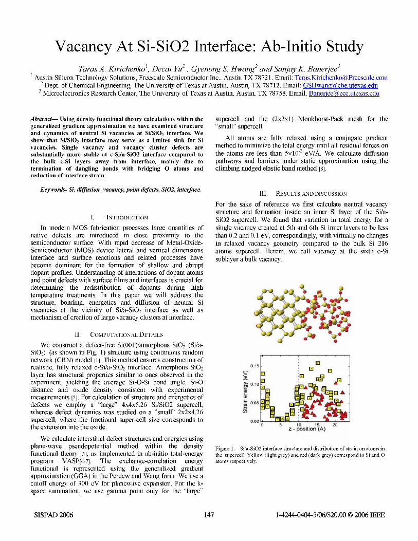
We construct a defect-free Si(001)/amorphous SiO2 (Si/a-SiO2) (as shown in Fig. 1) structure using continuous randomnetwork (CRN) model [1]. This method ensures construction ofrealistic, fully relaxed c-Si/a-SiO2 interface. Amorphous SiO2layer has structural properties similar to ones observed in theexperiment, yielding the average Si-O-Si bond angle, Si-Odistance and oxide density consistent with experimentalmeasurements [2]. For calculation of structure and energetics ofdefects we employ a "large" 4x4x5.26 Si/SiO2 supercell,whereas defect dynamics was studied on a "small" 2x2x4.26supercell, where the fractional super-cell size corresponds tothe extension into the oxide.
We calculate interstitial defect structures and energies usingplane-wave pseudopotential method within the densityfunctional theory [3], as implemented in ab-initio total-energyprogram VASP[4-7]. The exchange-correlation energyfunctional is represented using the generalized gradientapproximation (GGA) in the Perdew and Wang form. We use acutoff energy of 300 eV for planewave expansion. For the k-space summation, we use gamma point only for the "large"
supercell and the (2x2xl) Monkhorst-Pack mesh for the"small" supercell.
All atoms are fully relaxed using a conjugate gradientmethod to minimize the total energy until all residual forces onthe atoms are less than 5x10⁻² eV/A. We calculate diffusionpathways and barriers under static approximation using theclimbing nudged elastic band method [8].
III. RESULTS AND DISCUSSION
For the sake of reference we first calculate neutral vacancystructure and formation inside an inner Si layer of the Si/a-SiO2 supercell. We found that variation in total energy for asingle vacancy created at 5th and 6th Si inner layers to be lessthan 0.2 and 0.1 eV, correspondingly, with virtually no changesin relaxed vacancy geometry compared to the bulk Si 216atoms supercell. Herein, we call vacancy at the sixth c-Sisublayer a bulk vacancy.
id 0
z- pos tion A)
Figure 1. Si/a-SiO2 interface structure and distribution of strain on atoms inthe supercell. Yellow (light grey) and red (dark grey) correspond to Si and 0atoms respectively.
1-4244-0404-5/06/$20.00 © 2006 IEEE
..........".............iII
_4 a F-
A!
A('
SISPAD 2006 147

A. Interface VacancyTo create the interface vacancy we remove a Si atom from
the interface Si-O-Si bridge and relax the configuration (Fig. 2a)). Upon structure relaxation all atoms in the interface vacancystructure become fully coordinated. As a result, the interfacevacancy structure does not have any dangling bonds at all andis expected to be much more energetically stable compared tovacancies in inner Si layers. The interface vacancy structure isexamined at eighteen different locations. The most and leaststable states are respectively 1.9 eV more and 0.8 eV less stablethan the bulk vacancy, with the average energy reduction ofabout 1.0 eV. Vacancy stabilization at the interface isfacilitated by rearrangement of interface 0 atoms andformation of strong Si-O bonds with vacancy neighbors. Theabove stabilization strongly depends on the a-SiO2 networktopology near the interface vacancy site. At elevatedtemperatures formation of the interface vacancy may introducetopology changes in amorphous oxide network, leading tofarther stabilization. In addition, the vacancy may migratealong the interface to more energetically favorable location.
B. Sub-interface VacancyAt the first two Si layers under the interface we find the
vacancy formation energy to be reduced by 0.9 eV to 1.3 eV.As can be seen from the Fig. 1, removal of one atom from theSi layer provides immediate strain relief for the vacancy'snearest neighbors located in the first few atomic layers aroundinterface. Furthermore, upon the vacancy structure relaxationadditional reduction of strain in the second and third nearestneighbor shells occurs. We therefore suggest that one of themajor sources of vacancy stabilization at Si layers is the strain-assisted pairing and the immediate strain relief. Indeed, relaxedvacancy structures at the second and third sublayers showsignificant inward relaxation compared to the bulk. Forvacancy at third sublayer the most significant stabilization isobserved for vacancies created directly under the Si-O-Sibridge, where vacancies on average are 1.2 eV more stablecompared to the bulk vacancies.
We carefully examine the influence of the interface on theelectronic structure of the sub-interface and interface vacancy.In unrelaxed vacancy structure one of the vacancy-induceddefect levels is created inside the valence band manifold andthe one triply degenerate level inside the band gap. The bandgap level is unstable with respect to distortion due to the orbitaldegeneracy. As vacancy structure relaxes, Jahn-Teller (JT)distortion lows the symmetry and partially remove degeneracyof the triplet, splitting it into two levels in the band gap. Thispairing will sweep defects states from the band gap. The effectof pairing close to interface is well reflected in the vacancyDOS and should be distinguished from the pure strain reliefeffect discussed earlier.
Besides pure effect of strain assisted pairing we should alsotake into account possible interaction between vacancy statesand the states close in energy that are induced by distorted Sibonds near the interface as well as by interface sub-oxidized Siatoms. Although it is difficult to distinguish between thisresonance effect and strain-assisted pairing, we can gain someinsight by comparing vacancy stabilization under Si/a-SiO2with Si/c-SiO2 interface. Both interfaces have comparable
oxidation-induced strain. However, the interface states Si/a-SiO2 inherently have broader spectrum compared to the Si/c-SiO2. Thus coupling of the interface-induced states withvacancy defect states is more feasible in case of Si/a-SiO2. Thismay explain why we observe much smaller vacancystabilization of 0.6 eV under Si/C-SiO2.
Besides pure effect of strain assisted pairing we shouldalso take into account possible interaction between vacancystates and the states close in energy that are induced bydistorted Si bonds near the interface as well as by interfacesub-oxidized Si atoms. Although it is difficult to distinguishbetween this resonance effect and strain-assisted pairing, wecan gain some insight by comparing vacancy stabilizationunder Si/a-SiO2 with Si/c-SiO2 interface. Both interfaces havecomparable oxidation-induced strain. However, the interfacestates Si/a-SiO2 inherently have broader spectrum compared tothe Si/c-SiO2. Thus coupling of the interface-induced stateswith vacancy defect states is more feasible in case of Si/a-SiO2. This may explain why we observe much smallervacancy stabilization of 0.6 eV under Si/c-SiO2.
C. Vacancy Clustering at Si/a-SiO2 InterfaceWe check interface di-vacancy (DV) configurations at
several interface locations. For DV construction we removetwo Si atoms from an interface Si-O-Si bridge and rearrangeremaining unpaired 0 atoms such that the four-foldcoordination of all remaining atoms in the supercell isrecovered (Fig. 2 b)). For all tested configurations pairing oftwo single vacancies into a DV leads to an additional energyreduction per vacancy ranging from 0.2 eV to 0.8 eV. Themost stable interface DV is 1.8 eV more stable compared to aDV at 5th and 6t c-Si sublayers of the Si/a-SiO2 supercell.
As widely known, cluster formation energy per vacancydecreases with cluster size. Contrary to above, adding anothervacancy to an interface DV does not lead to considerableincrease in stabilization per vacancy. Advantages of danglingbonds removal are achieved at the expense of increased strainenergy. The later imposes an upper limit on the number ofvacancies that can be accommodated at the interface. The Si/a-SiO2 interface can absorb up to up to a monolayer (7x10¹⁴ /cm2) of vacancies without undergoing step or void formation.
(a) (b)Figure 2. a) relaxed interface vacancy structure b) relaxed interface di-vacancy structure. Positions of the removed Si atoms are shown by dark bluecircles. Note that the coordination of all atoms is restored.
1-4244-0404-5/06/$20.00 © 2006 IEEESISPAD 2006 148

(a) (b)
Figure 3. Vacancy migration pathway: a) from bulk layer to theinterface b) along the interface. Frame sequence is top to bottom,with saddle point illustrated at middle. Direction of atomdisplacements is shown by blue arrows. Yellow (light grey) and red(dark grey) correspond to Si and 0 atoms respectively.
D. Vacancy Dynamics at Si/a-SiO2 Interface
To identify a possible mechanism of a single vacancyformation at Si/a-SiO2 interface, we calculate the migrationpathway of a vacancy to the interface from a c-Si sublayer(Fig.3 a)). We test four different locations and find the rangeof migration barriers from 0.1 eV to 1.3 eV, with the averagemigration barrier of 0.8 eV. The return barrier is found to beat least 0.5 eV higher since as a surface vacancy is generallymore stable compared to the subsurface one. The wide rangeof migration barriers and the higher return barrier suggest that
the interface might be an effective sink for vacancies even atlow temperatures.
We also calculate the energy barrier and the pathway forvacancy migration along interface (Fig.3 b)). Migrationbarriers for pathways between the chosen three pairs ofneighboring interface vacancies are found to be 0.4-0.8 eV.Thus at a sufficiently high temperature an interface vacancycan migrate along the Si-O-Si row before either it is trapped atthe low energy location or combined with another vacancy inthe same row forming a more stable DV defect.
IV. CONCLUSIONIn summary, we found that vacancy formation energy at
interface is reduced up to 1.9 eV, and even larger stabilizationpossible for interface vacancy clusters. We attribute thisstabilization to the two factors: i) strain relief c-Si sub-layersunder Si/a-SiO2 interface, and ii) strain-assisted pairingbetween vacancy neighbors and the effect change ofperiodicity and a chemical composition of the system on theelectronic states associated with a vacancy. We found that avacancy can migrate easily form bulk Si layers to theinterface. Clustering can farther reduce vacancy formation atinterface. We may conclude that Si/a-SiO2 interface may serveas a (limited) sink for neutral vacancies.
ACKNOWLEDGMENTAll our calculations were performed using supercomputers atthe Texas Advanced Computing Center (TACC) at theUniversity of Texas at Austin.This work was supported in part by Semiconductor ResearchCorporation, Task ID 1413.00 1.
REFERENCES
[1] F. Wooten et al, Phys.Rev.Lett. 54,1392 (1985)[2] A. Brunet-Bruneau et al, JVST A 16, 2281(1998)[3] W. Kohn and L.J. Sham, Phys. Rev. 140, A1133 (1965)[4] G. Kresse and J. Hafner, Phys. Rev. B 47, 558 (1993); ibid. 49, 14251
(1994)[5] G. Kresse and J. Furthmuller, Comput. Mat. Sci/ 6. 15 (1996)[6] G. Kresse and J.Furthmuller, Phys.Rev.B 55, 11169(1996)[7] G. Kresse and J. Hafner, J. Phys.: Condens. Matter 6, 8245 (1994)[8] G. Henkelman et al, J. Chem. Phys., 113, 9901 (2000)
1-4244-0404-5/06/$20.00 © 2006 IEEESISPAD 2006 149