Tektronix - Fundamentals of Signal Integrity - Techni … · Fundamentals of Signal Integrity ......
17
1547 N. Trooper Road • P. O. Box 1117 • Worcester, PA 19490-1117 USA Corporate Phone: 610-825-4990 • Sales: 800-832-4866 or 610-941-2400 Fax: 800-854-8665 or 610-828-5623 • Web: www.techni-tool.com Fundamentals of Signal Integrity Our thanks to Tektronix for allowing us to reprint the following article. Signal Integrity Described By definition, “integrity” means “complete and unimpaired.” Likewise, a digital signal with good integrity has clean, fast transitions; stable and valid logic levels; accurate placement in time and it would be free of any transients. Evolving technology makes it increasingly difficult for system developers to produce and maintain complete, unimpaired signals in digital systems. The purpose of this primer is to provide some insight into signal integrity-related problems in digital systems, and to describe their causes, characteristics, effects, and solutions. Digital Technology and the Information Age It’s been over twenty years since the personal computer emerged and almost as long since cellular telephony went from being a novelty to a consumer necessity. For both, one trend has remained constant: the demand for more features and services, and the need for more bandwidth to deliver them. First-generation PC users were excited about the power of creating a simple spreadsheet. Now they demand detailed graphics, high- quality audio, and fast-streaming video. And, cell phones are hardly a tool anymore for just conversation. Our much-smaller world now depends on increasingly more content and its rapid, reliable delivery. The term “Information Age” was coined to describe this new interwoven, interdependent, data-based culture. With the Information Age has come a steady stream of technology breakthroughs in the fields of semiconductors, PC bus architectures, network infrastructures, and digital wireless communications. In PCs— and especially in servers— processor speeds have escalated into the multi-GHz range, and memory throughput and internal bus speeds have risen right along with them. These dramatically increased rates support computer applications such as 3D games and computer-aided design programs. Sophisticated 3D imagery requires a huge amount of bandwidth at the circuit board level, where the CPU, the graphics subsystem, and the memory has to move data, constantly, as the image moves. Computers are just one facet of the bandwidth-hungry Information Age. Digital communication equipment designers (and particularly those developing the electrical and optical infrastructure elements for both mobile and fixed networks) are moving toward 40 Gb/s data rates. And digital video product development teams are designing a new generation of transmission equipment for high-definition, interactive video. Numerous technologies are pushing these data rate advancements. Serial buses are emerging to break the speed barriers inherent in older, parallel bus architectures. In some cases, system clocks are intentionally dithered to reduce unintended radiated emissions. And smaller, denser circuit boards using ball grid array ICs and buried vias have become common as developers look for ways to maximize density and minimize path lengths. Rising Bandwidth Challenges Digital Design Today’s digital bandwidth race requires innovative thinking. Bus cycle times are now up to a thousand times faster than they were twenty years ago. Transactions that once took microseconds are now measured in nanoseconds. To achieve this improvement, edge speeds today are now a hundred times faster than before. Circuit board technology, however, has not kept pace because of certain physical realities. The propagation time of inter-chip buses has remained virtually unchanged. Although geometries have shrunk, circuit boards still need sufficient space for IC devices, connectors, passive components, and of course, the bus traces themselves. This space equates to distance, and distance means delay— the enemy of speed. It’s important to remember that the edge speed – or rise time – of a digital signal can carry much higher frequency components than its repetition rate might imply. It’s actually the higher frequency components that
Transcript of Tektronix - Fundamentals of Signal Integrity - Techni … · Fundamentals of Signal Integrity ......
1547 N. Trooper Road • P. O. Box 1117 • Worcester, PA 19490-1117 USA Corporate Phone: 610-825-4990 • Sales: 800-832-4866 or 610-941-2400
Fax: 800-854-8665 or 610-828-5623 • Web: www.techni-tool.com
Fundamentals of Signal Integrity
Our thanks to Tektronix for allowing us to reprint the following article.
Signal Integrity Described By definition, “integrity” means “complete and unimpaired.” Likewise, a digital signal with good integrity has clean, fast transitions; stable and valid logic levels; accurate placement in time and it would be free of any transients. Evolving technology makes it increasingly difficult for system developers to produce and maintain complete, unimpaired signals in digital systems. The purpose of this primer is to provide some insight into signal integrity-related problems in digital systems, and to describe their causes, characteristics, effects, and solutions. Digital Technology and the Information Age It’s been over twenty years since the personal computer emerged and almost as long since cellular telephony went from being a novelty to a consumer necessity. For both, one trend has remained constant: the demand for more features and services, and the need for more bandwidth to deliver them. First-generation PC users were excited about the power of creating a simple spreadsheet. Now they demand detailed graphics, high-quality audio, and fast-streaming video. And, cell phones are hardly a tool anymore for just conversation. Our much-smaller world now depends on increasingly more content and its rapid, reliable delivery. The term “Information Age” was coined to describe this new interwoven, interdependent, data-based culture. With the Information Age has come a steady stream of technology breakthroughs in the fields of semiconductors, PC bus architectures, network infrastructures, and digital wireless communications. In PCs— and especially in servers— processor speeds have escalated into the multi-GHz range, and memory throughput and internal bus speeds have risen right along with them. These dramatically increased rates support computer applications such as 3D games and computer-aided design programs. Sophisticated 3D imagery requires a
huge amount of bandwidth at the circuit board level, where the CPU, the graphics subsystem, and the memory has to move data, constantly, as the image moves. Computers are just one facet of the bandwidth-hungry Information Age. Digital communication equipment designers (and particularly those developing the electrical and optical infrastructure elements for both mobile and fixed networks) are moving toward 40 Gb/s data rates. And digital video product development teams are designing a new generation of transmission equipment for high-definition, interactive video. Numerous technologies are pushing these data rate advancements. Serial buses are emerging to break the speed barriers inherent in older, parallel bus architectures. In some cases, system clocks are intentionally dithered to reduce unintended radiated emissions. And smaller, denser circuit boards using ball grid array ICs and buried vias have become common as developers look for ways to maximize density and minimize path lengths. Rising Bandwidth Challenges Digital Design Today’s digital bandwidth race requires innovative thinking. Bus cycle times are now up to a thousand times faster than they were twenty years ago. Transactions that once took microseconds are now measured in nanoseconds. To achieve this improvement, edge speeds today are now a hundred times faster than before. Circuit board technology, however, has not kept pace because of certain physical realities. The propagation time of inter-chip buses has remained virtually unchanged. Although geometries have shrunk, circuit boards still need sufficient space for IC devices, connectors, passive components, and of course, the bus traces themselves. This space equates to distance, and distance means delay— the enemy of speed. It’s important to remember that the edge speed – or rise time – of a digital signal can carry much higher frequency components than its repetition rate might imply. It’s actually the higher frequency components that
1547 N. Trooper Road • P. O. Box 1117 • Worcester, PA 19490-1117 USA Corporate Phone: 610-825-4990 • Sales: 800-832-4866 or 610-941-2400
Fax: 800-854-8665 or 610-828-5623 • Web: www.techni-tool.com
create the desired fast transitions in a digital signal. With today’s high-speed serial buses, there is often significant energy at the 5th harmonic of the clock rate. As a result, circuit board traces just six inches long become transmission lines when driven with signals exhibiting edge rates below four to six nanoseconds. Circuit board traces are no longer simple conductors. At lower frequencies, a trace exhibits mostly resistive characteristics. As frequencies increase, a trace begins to act like a capacitor. At the highest frequencies, a trace’s inductance plays a larger role. Signal integrity problems increase at higher frequencies. Transmission line effects are critical. Impedance discontinuities along the signal path create reflections, which degrade signal edges. Crosstalk increases. Power supply decoupling becomes far less effective, as ground planes and power planes become inductive and act like transmission lines. EMI (electromagnetic interference) goes up as faster edge speeds produce shorter wavelengths relative to the bus length, which creates unintended radiated emissions. These emissions increase crosstalk and can cause a digital device to fail EMC (electromagnetic compliance) testing. Faster edge speeds generally also require higher currents to produce them. Higher currents tend to cause ground bounce, especially on wide buses in which many signals switch at once. Also, higher current increases the amount of radiated magnetic energy and, with it, crosstalk. As data rates increase to the gigabit range and beyond, digital designers face all the frustrations that come with high frequency design. An ideal digital pulse is cohesive in time and amplitude, is free from deviations and jitter, and has fast, clean transitions. As system speeds increase it becomes increasingly more difficult to maintain ideal signal characteristics, requiring careful consideration of signal integrity issues. Review of Signal Integrity Concepts At frequencies in the gigahertz range, a host of variables can affect signal integrity: signal path design, impedances and loading, transmission line effects, and even power distribution on or off the circuit board. The design engineer’s mission is to minimize these problems from the start, and to correct them when they do appear. To do that, they must investigate both of the fundamental sources of signal degradation: digital issues and analog issues.
Problems Created by Digital Timing Issues An engineer working with an evolving digital system design is likely to encounter signal integrity problems in their digital form. Binary signals on the bus or device outputs produce incorrect values. The errors may appear in the waveform (timing measurement) view on a logic analyzer, and they may also show up at the state or even the protocol level. It only takes one bad bit to dramatically affect the outcome of an instruction or transaction. Digital signal aberrations stem from many root causes. Timing-related issues are especially common:
• Bus Contention - Bus contention occurs when two driver devices try to use the same bus line at the same time. Normally, one of the drivers should go to a high impedance state and not hinder the other while it sends data. If the high impedance device doesn’t change in time, the two drivers then contend for the bus. Neither driver prevails, forcing the bus to an indeterminate amplitude that may fail to reach the threshold voltage. This creates, for example, a “0” logic level where there should be a “1.” With a high-speed bus, this situation is complicated further by the time of flight between the contending sources and the receiver.
Every Design Detail is Important At clock frequencies in the hundreds of megahertz and above, every design detail is important to minimize signal integrity problems:
• Clock distribution • Signal path design • Stubs • Noise margin • Impedances and loading • Transmission line effects • Signal path return currents • Termination • Decoupling • Power distribution
• Setup and Hold Violations - Setup and hold violations are increasing as digital systems push to faster speeds. A clocked device, such as a D flip flop, requires the data to be stable at its input for a specified time before the clock arrives. This is known as “setup” time. Similarly, the input data must remain valid for a specified time after the leading edge of the clock. This is known as “hold” time. Violating setup and/or hold requirements can cause unpredictable glitches on the output, or can cause there to be no output transition at all. Setup and hold times are decreasing as device speeds increase, making the timing relationships harder to troubleshoot.
1547 N. Trooper Road • P. O. Box 1117 • Worcester, PA 19490-1117 USA Corporate Phone: 610-825-4990 • Sales: 800-832-4866 or 610-941-2400
Fax: 800-854-8665 or 610-828-5623 • Web: www.techni-tool.com
• Metastability - Metastability is an indeterminate or unstable data state that results from a timing violation, such as a setup and hold problem. As a result, the output signal might be late or achieve an illegal output level, such as a runt, a glitch, or even the wrong logic level.
• Undefined Conditions - Undefined conditions can
occur when the switching states on multiple inputs of a logic device are not correctly aligned in time. This may be caused by variations or errors in the delay on these input signals.
• Inter-Symbol Interference (ISI) - ISI is when one
symbol interferes with subsequent symbols, creating distortion of the signal. It is caused by jitter and noise due to high frequency losses and reflections.
Logic analyzers have powerful tools to help users acquire and analyze digital signals in many formats. Today’s advanced logic analyzers can capture data from thousands of test points simultaneously, then display streams of digital pulses and their placement in time relative to each another. With this type of conventional logic analyzer acquisition, amplitude errors and glitches can appear to be valid logic levels even though they contain incorrect data. It may be possible to see an error value in the hexadecimal code, for example, but the display won’t show why the error is occurring. It can be very difficult to find the cause of a logic error if there is no means to probe further into the signal’s behavior. Isolating Analog Deviations Many digital problems are much easier to pinpoint if you can probe deeply into the signal’s behavior and see the analog representation of the flawed digital signal. Although the problem may appear as a misplaced digital pulse, the cause of the problem signal often is due to its analog characteristics. Analog characteristics can become digital faults when low-amplitude signals turn into incorrect logic states, or when slow rise times cause pulses to shift in time. Seeing a digital pulse stream with a simultaneous analog view of the same pulses is the first step in tracking down these kinds of problems. Oscilloscopes are commonly used to identify the root cause of signal integrity problems by analyzing a signal’s analog characteristics. They can display waveform details, edges and noise, and they can also detect and display transients. With powerful triggering and analysis features, an oscilloscope can track down analog aberrations and help the design engineer find device problems causing faults. Common causes of analog deviations:
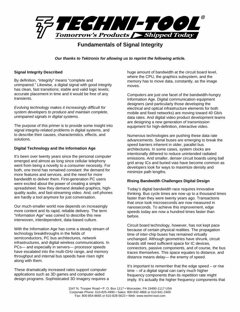
Figure 1. Amplitude problems. Amplitude Problems – Amplitude problems include ringing (oscillation), “droop” (decreased amplitude at the start of a pulse), and “runt” pulses (those which don’t reach full amplitude).
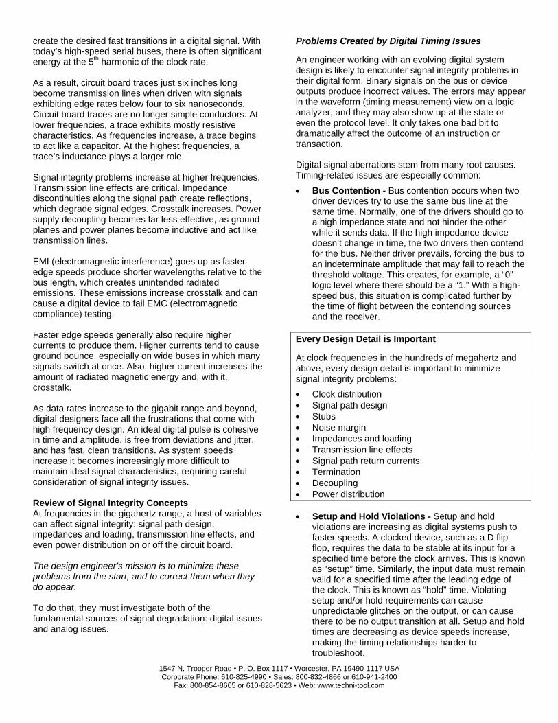
Figure 2. Edge aberrations. Edge Aberrations – Edge aberrations can result from board layout problems or from improper termination or even quality problems in the semiconductor devices. Aberrations can include preshoot, rounding, overshoot, ringing, and slow rise time.
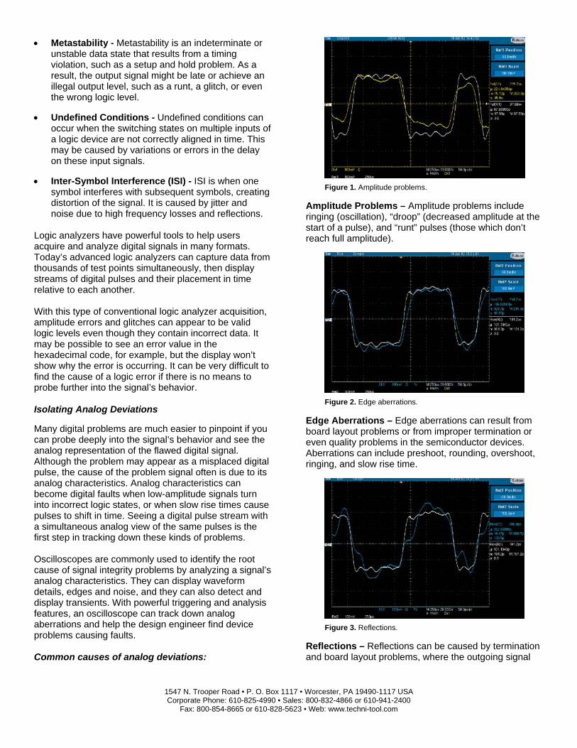
Figure 3. Reflections. Reflections – Reflections can be caused by termination and board layout problems, where the outgoing signal
1547 N. Trooper Road • P. O. Box 1117 • Worcester, PA 19490-1117 USA Corporate Phone: 610-825-4990 • Sales: 800-832-4866 or 610-941-2400
Fax: 800-854-8665 or 610-828-5623 • Web: www.techni-tool.com
bounces back toward its source and interferes with subsequent pulses.
Figure 4. Crosstalk. Crosstalk – Crosstalk can occur when long traces running next to each other couple their signals together through mutual capacitance and inductance. In addition, the higher current embodied in fast edges increases the amount of radiated magnetic energy, and with it, crosstalk.
Figure 5. Ground bounce. Ground Bounce – Ground bounce, caused by excessive current draw (and/or resistance in the power supply and ground return paths), can cause a circuit’s ground reference level to shift when current demands are high.
Figure 6. Jitter.
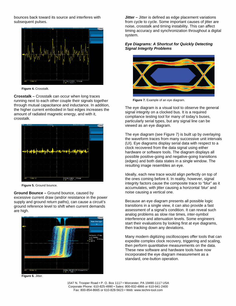
Jitter – Jitter is defined as edge placement variations from cycle to cycle. Some important causes of jitter are noise, crosstalk and timing instability. This can affect timing accuracy and synchronization throughout a digital system. Eye Diagrams: A Shortcut for Quickly Detecting Signal Integrity Problems
Figure 7. Example of an eye diagram. The eye diagram is a visual tool to observe the general signal integrity on a clocked bus. It is a required compliance testing tool for many of today’s buses, particularly serial types, but any signal line can be viewed as an eye diagram. The eye diagram (see Figure 7) is built up by overlaying the waveform traces from many successive unit intervals (UI). Eye diagrams display serial data with respect to a clock recovered from the data signal using either hardware or software tools. The diagram displays all possible positive-going and negative-going transitions (edges) and both data states in a single window. The resulting image resembles an eye. Ideally, each new trace would align perfectly on top of the ones coming before it. In reality, however, signal integrity factors cause the composite trace to “blur” as it accumulates, with jitter causing a horizontal ‘blur’ and noise causing a vertical one. Because an eye diagram presents all possible logic transitions in a single view, it can also provide a fast assessment of a signal’s condition. It can reveal such analog problems as slow rise times, inter-symbol interference and attenuation levels. Some engineers start their evaluations by looking first at eye diagrams, then tracking down any deviations. Many modern digitizing oscilloscopes offer tools that can expedite complex clock recovery, triggering and scaling, then perform quantitative measurements on the data. These new software and hardware tools have now incorporated the eye diagram measurement as a standard, one-button operation.
1547 N. Trooper Road • P. O. Box 1117 • Worcester, PA 19490-1117 USA Corporate Phone: 610-825-4990 • Sales: 800-832-4866 or 610-941-2400
Fax: 800-854-8665 or 610-828-5623 • Web: www.techni-tool.com
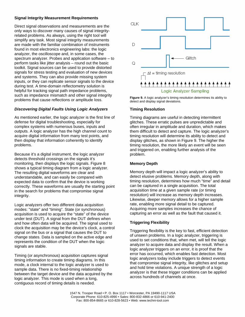
Signal Integrity Measurement Requirements Direct signal observations and measurements are the only ways to discover many causes of signal integrity-related problems. As always, using the right tool will simplify any task. Most signal integrity measurements are made with the familiar combination of instruments found in most electronics engineering labs: the logic analyzer, the oscilloscope and, in some cases, the spectrum analyzer. Probes and application software – to perform tasks like jitter analysis – round out the basic toolkit. Signal sources can be used to provide distorted signals for stress testing and evaluation of new devices and systems. They can also provide missing system inputs, or they can replicate sensor signals to the device during test. A time-domain reflectometry solution is helpful for tracking signal path impedance problems, such as impedance mismatch and other signal integrity problems that cause reflections or amplitude loss. Discovering Digital Faults Using Logic Analyzers As mentioned earlier, the logic analyzer is the first line of defense for digital troubleshooting, especially for complex systems with numerous buses, inputs and outputs. A logic analyzer has the high channel count to acquire digital information from many test points, and then display that information coherently to identify problems. Because it’s a digital instrument, the logic analyzer detects threshold crossings on the signals it’s monitoring, then displays the logic signals. Figure 8 shows a typical timing diagram from a logic analyzer. The resulting digital waveforms are clear and understandable, and can easily be compared with expected data to confirm that the device is working correctly. These waveforms are usually the starting point in the search for problems that compromise signal integrity. Logic analyzers offer two different data acquisition modes: "state" and “timing”. State (or synchronous) acquisition is used to acquire the “state” of the device under test (DUT). A signal from the DUT defines when and how often data will be acquired. The signal used to clock the acquisition may be the device’s clock, a control signal on the bus or a signal that causes the DUT to change states. Data is sampled on the active edge and represents the condition of the DUT when the logic signals are stable. Timing (or asynchronous) acquisition captures signal timing information to create timing diagrams. In this mode, a clock internal to the logic analyzer is used to sample data. There is no fixed-timing relationship between the target device and the data acquired by the logic analyzer. This mode is used when a long, contiguous record of timing details is needed.
Figure 9. A logic analyzer’s timing resolution determines its ability to detect and display signal deviations. Timing Resolution Timing diagrams are useful in detecting intermittent glitches. These erratic pulses are unpredictable and often irregular in amplitude and duration, which makes them difficult to detect and capture. The logic analyzer’s timing resolution will determine its ability to detect and display glitches, as shown in Figure 9. The higher the timing resolution, the more likely an event will be seen and triggered on, enabling further analysis of the problem. Memory Depth Memory depth will impact a logic analyzer’s ability to detect elusive problems. Memory depth, along with timing resolution, determines how much “time” and detail can be captured in a single acquisition. The total acquisition time at a given sample rate (or timing resolution) will increase as memory depth increases. Likewise, deeper memory allows for a higher sample rate, enabling more signal detail to be captured. Acquiring more samples increases the chance of capturing an error as well as the fault that caused it. Triggering Flexibility Triggering flexibility is the key to fast, efficient detection of unseen problems. In a logic analyzer, triggering is used to set conditions that, when met, will tell the logic analyzer to acquire data and display the result. When a logic analyzer triggers on an error, it is proof that the error has occurred, which enables fast detection. Most logic analyzers today include triggers to detect events that compromise signal integrity, like glitches and setup and hold time violations. A unique strength of a logic analyzer is that these trigger conditions can be applied across hundreds of channels at once.
1547 N. Trooper Road • P. O. Box 1117 • Worcester, PA 19490-1117 USA Corporate Phone: 610-825-4990 • Sales: 800-832-4866 or 610-941-2400
Fax: 800-854-8665 or 610-828-5623 • Web: www.techni-tool.com
With its ability to analyze hundreds to thousands of digital lines at a time, the logic analyzer is a powerful tool for discovering device faults for further analysis. For fast and efficient debugging, it’s important to carefully look at usability features like triggering, as well as performance attributes, when choosing a logic analyzer solution. Logic Analyzer Probing Solutions A logic analyzer’s probing scheme plays a critical role in high-speed digital acquisition. It's critical that the probe deliver the signal to the logic analyzer with the highest possible fidelity. Most logic analyzer probes fulfill this fundamental requirement, but some take the concept even further. Some logic analyzers require separate probing connections for timing and state acquisitions. This is known as “double probing”, which is a technique that can compromise the signal environment, affecting the actual measurements themselves. For example, connecting two probes at once to the test point can create unacceptable levels of signal loading. Connecting them individually exposes the test point to double the risk of damage or misconnection. Moreover, it is time-consuming to connect two probes. Some logic analyzers have the ability to measure both timing and state acquisitions through one probe. This simultaneous timing/state acquisition speeds troubleshooting and supports signal integrity analysis tasks by minimizing the impact of probes on the DUT. Recent advancements have taken logic analyzer probing technology to a new level. The latest generation of probes can carry both digital information to the logic analyzer while also delivering the same information to an oscilloscope as analog signals. Any pin of the probe can be used for both digital and analog acquisition. The analog signal routes through the logic analyzer to an external oscilloscope, making it possible to determine, almost instantly, if a digital error is associated with an analog fault. In high performance digital systems, a dedicated test point is usually the most practical way to measure signals. Some dedicated test points are fitted with pins to simplify their connection with clip-on probes and leadsets. These types of test connectors have an effect on the target device’s signal environment, even when they aren’t connected to a logic analyzer. A logic analyzer’s probes can also mount to dedicated connectors on the DUT. The matched impedance connector, MICTOR, is a compact, high-density connector joined to a matching connector on the logic analyzer probe. Board-mounted connectors add cost to the target device, and they can affect high-speed signal operation, but they do provide fast, positive connections.
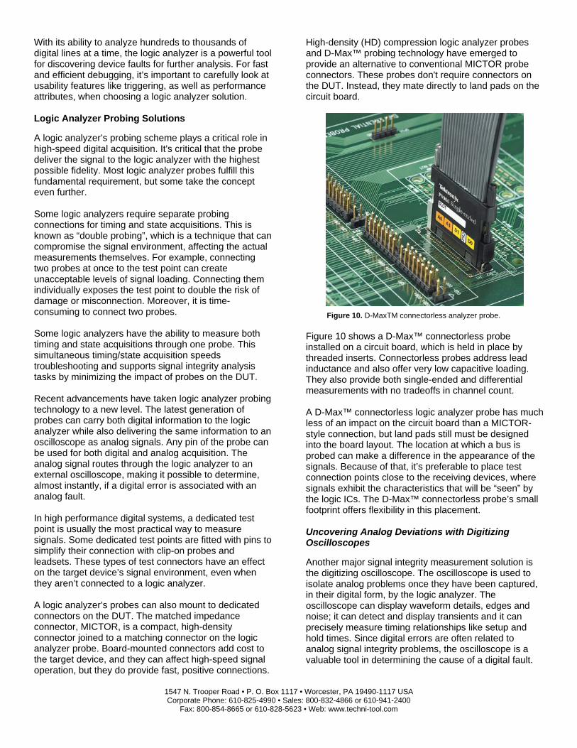
High-density (HD) compression logic analyzer probes and D-Max™ probing technology have emerged to provide an alternative to conventional MICTOR probe connectors. These probes don't require connectors on the DUT. Instead, they mate directly to land pads on the circuit board.
Figure 10. D-MaxTM connectorless analyzer probe. Figure 10 shows a D-Max™ connectorless probe installed on a circuit board, which is held in place by threaded inserts. Connectorless probes address lead inductance and also offer very low capacitive loading. They also provide both single-ended and differential measurements with no tradeoffs in channel count. A D-Max™ connectorless logic analyzer probe has much less of an impact on the circuit board than a MICTOR-style connection, but land pads still must be designed into the board layout. The location at which a bus is probed can make a difference in the appearance of the signals. Because of that, it’s preferable to place test connection points close to the receiving devices, where signals exhibit the characteristics that will be “seen” by the logic ICs. The D-Max™ connectorless probe’s small footprint offers flexibility in this placement. Uncovering Analog Deviations with Digitizing Oscilloscopes Another major signal integrity measurement solution is the digitizing oscilloscope. The oscilloscope is used to isolate analog problems once they have been captured, in their digital form, by the logic analyzer. The oscilloscope can display waveform details, edges and noise; it can detect and display transients and it can precisely measure timing relationships like setup and hold times. Since digital errors are often related to analog signal integrity problems, the oscilloscope is a valuable tool in determining the cause of a digital fault.
1547 N. Trooper Road • P. O. Box 1117 • Worcester, PA 19490-1117 USA Corporate Phone: 610-825-4990 • Sales: 800-832-4866 or 610-941-2400
Fax: 800-854-8665 or 610-828-5623 • Web: www.techni-tool.com
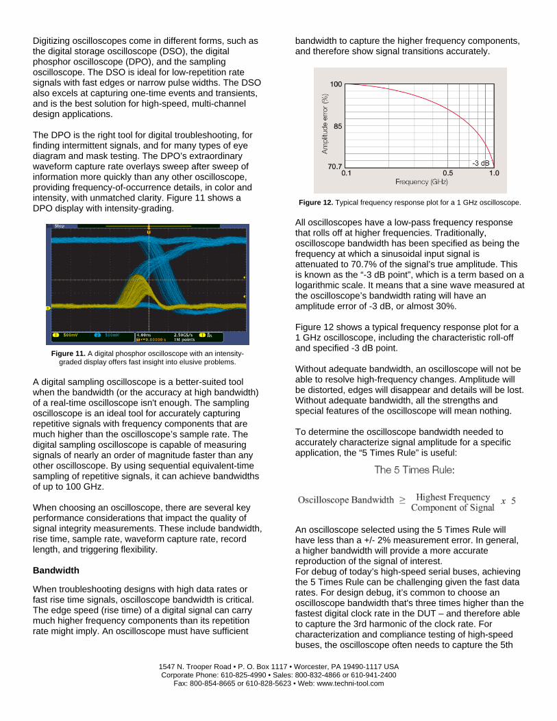
Digitizing oscilloscopes come in different forms, such as the digital storage oscilloscope (DSO), the digital phosphor oscilloscope (DPO), and the sampling oscilloscope. The DSO is ideal for low-repetition rate signals with fast edges or narrow pulse widths. The DSO also excels at capturing one-time events and transients, and is the best solution for high-speed, multi-channel design applications. The DPO is the right tool for digital troubleshooting, for finding intermittent signals, and for many types of eye diagram and mask testing. The DPO’s extraordinary waveform capture rate overlays sweep after sweep of information more quickly than any other oscilloscope, providing frequency-of-occurrence details, in color and intensity, with unmatched clarity. Figure 11 shows a DPO display with intensity-grading.
Figure 11. A digital phosphor oscilloscope with an intensity- graded display offers fast insight into elusive problems.
A digital sampling oscilloscope is a better-suited tool when the bandwidth (or the accuracy at high bandwidth) of a real-time oscilloscope isn't enough. The sampling oscilloscope is an ideal tool for accurately capturing repetitive signals with frequency components that are much higher than the oscilloscope’s sample rate. The digital sampling oscilloscope is capable of measuring signals of nearly an order of magnitude faster than any other oscilloscope. By using sequential equivalent-time sampling of repetitive signals, it can achieve bandwidths of up to 100 GHz. When choosing an oscilloscope, there are several key performance considerations that impact the quality of signal integrity measurements. These include bandwidth, rise time, sample rate, waveform capture rate, record length, and triggering flexibility. Bandwidth When troubleshooting designs with high data rates or fast rise time signals, oscilloscope bandwidth is critical. The edge speed (rise time) of a digital signal can carry much higher frequency components than its repetition rate might imply. An oscilloscope must have sufficient
bandwidth to capture the higher frequency components, and therefore show signal transitions accurately.
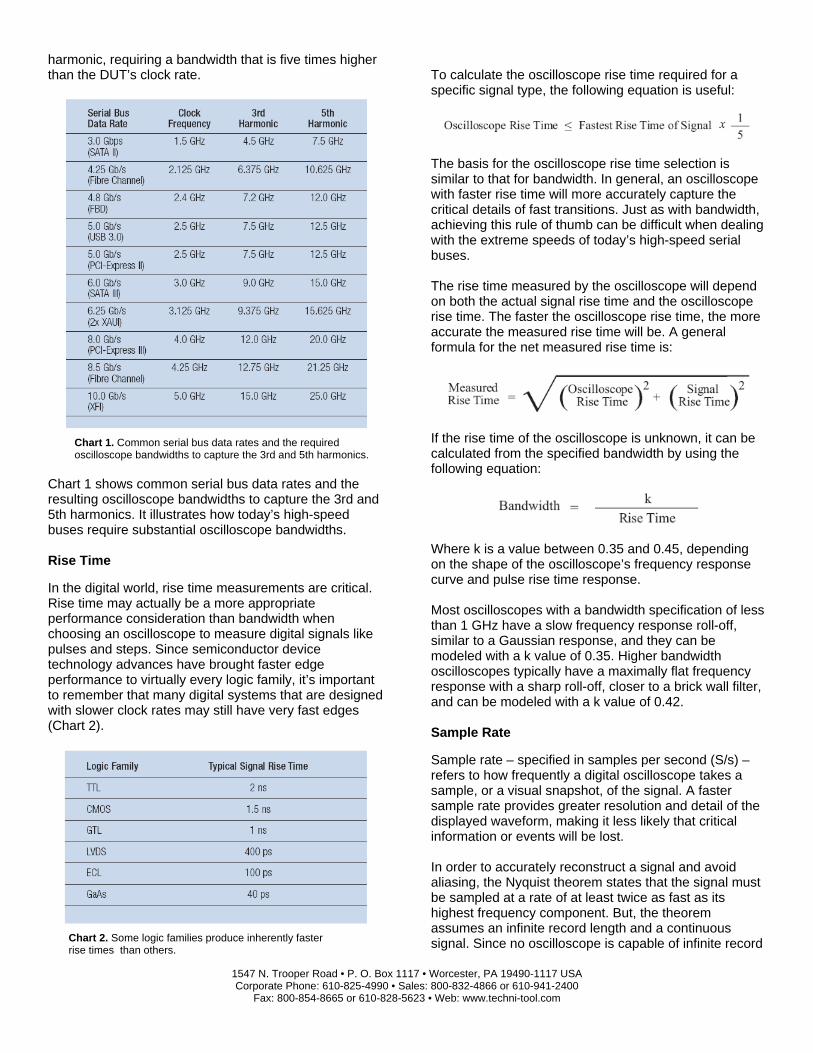
Figure 12. Typical frequency response plot for a 1 GHz oscilloscope.
All oscilloscopes have a low-pass frequency response that rolls off at higher frequencies. Traditionally, oscilloscope bandwidth has been specified as being the frequency at which a sinusoidal input signal is attenuated to 70.7% of the signal’s true amplitude. This is known as the “-3 dB point”, which is a term based on a logarithmic scale. It means that a sine wave measured at the oscilloscope’s bandwidth rating will have an amplitude error of -3 dB, or almost 30%. Figure 12 shows a typical frequency response plot for a 1 GHz oscilloscope, including the characteristic roll-off and specified -3 dB point. Without adequate bandwidth, an oscilloscope will not be able to resolve high-frequency changes. Amplitude will be distorted, edges will disappear and details will be lost. Without adequate bandwidth, all the strengths and special features of the oscilloscope will mean nothing. To determine the oscilloscope bandwidth needed to accurately characterize signal amplitude for a specific application, the “5 Times Rule” is useful:
An oscilloscope selected using the 5 Times Rule will have less than a +/- 2% measurement error. In general, a higher bandwidth will provide a more accurate reproduction of the signal of interest. For debug of today’s high-speed serial buses, achieving the 5 Times Rule can be challenging given the fast data rates. For design debug, it’s common to choose an oscilloscope bandwidth that's three times higher than the fastest digital clock rate in the DUT – and therefore able to capture the 3rd harmonic of the clock rate. For characterization and compliance testing of high-speed buses, the oscilloscope often needs to capture the 5th
1547 N. Trooper Road • P. O. Box 1117 • Worcester, PA 19490-1117 USA Corporate Phone: 610-825-4990 • Sales: 800-832-4866 or 610-941-2400
Fax: 800-854-8665 or 610-828-5623 • Web: www.techni-tool.com
harmonic, requiring a bandwidth that is five times higher than the DUT’s clock rate.
Chart 1. Common serial bus data rates and the required oscilloscope bandwidths to capture the 3rd and 5th harmonics. Chart 1 shows common serial bus data rates and the resulting oscilloscope bandwidths to capture the 3rd and 5th harmonics. It illustrates how today’s high-speed buses require substantial oscilloscope bandwidths. Rise Time In the digital world, rise time measurements are critical. Rise time may actually be a more appropriate performance consideration than bandwidth when choosing an oscilloscope to measure digital signals like pulses and steps. Since semiconductor device technology advances have brought faster edge performance to virtually every logic family, it’s important to remember that many digital systems that are designed with slower clock rates may still have very fast edges (Chart 2).
Chart 2. Some logic families produce inherently faster rise times than others.
To calculate the oscilloscope rise time required for a specific signal type, the following equation is useful:
The basis for the oscilloscope rise time selection is similar to that for bandwidth. In general, an oscilloscope with faster rise time will more accurately capture the critical details of fast transitions. Just as with bandwidth, achieving this rule of thumb can be difficult when dealing with the extreme speeds of today’s high-speed serial buses. The rise time measured by the oscilloscope will depend on both the actual signal rise time and the oscilloscope rise time. The faster the oscilloscope rise time, the more accurate the measured rise time will be. A general formula for the net measured rise time is:
If the rise time of the oscilloscope is unknown, it can be calculated from the specified bandwidth by using the following equation:
Where k is a value between 0.35 and 0.45, depending on the shape of the oscilloscope’s frequency response curve and pulse rise time response. Most oscilloscopes with a bandwidth specification of less than 1 GHz have a slow frequency response roll-off, similar to a Gaussian response, and they can be modeled with a k value of 0.35. Higher bandwidth oscilloscopes typically have a maximally flat frequency response with a sharp roll-off, closer to a brick wall filter, and can be modeled with a k value of 0.42. Sample Rate Sample rate – specified in samples per second (S/s) – refers to how frequently a digital oscilloscope takes a sample, or a visual snapshot, of the signal. A faster sample rate provides greater resolution and detail of the displayed waveform, making it less likely that critical information or events will be lost. In order to accurately reconstruct a signal and avoid aliasing, the Nyquist theorem states that the signal must be sampled at a rate of at least twice as fast as its highest frequency component. But, the theorem assumes an infinite record length and a continuous signal. Since no oscilloscope is capable of infinite record
1547 N. Trooper Road • P. O. Box 1117 • Worcester, PA 19490-1117 USA Corporate Phone: 610-825-4990 • Sales: 800-832-4866 or 610-941-2400
Fax: 800-854-8665 or 610-828-5623 • Web: www.techni-tool.com
length, and because, by definition, glitches aren't continuous, sampling at only twice the rate of the highest frequency component is usually insufficient. In reality, accurate reconstruction of a signal depends on both the sample rate and the interpolation method used to fill in the spaces between the samples. Some oscilloscopes offer sin(x)/x interpolation for measuring sinusoidal signals or linear interpolation for square waves, pulses, and other signal types. Waveform Capture Rate The waveform capture rate, expressed as waveforms per second (wfms/s), determines how frequently the oscilloscope captures a signal. While the sample rate indicates how frequently the oscilloscope samples the input signal within one waveform, or cycle, the waveform capture rate refers to how quickly an oscilloscope acquires the whole waveform. Oscilloscopes with high waveform capture rates provide significantly more visual insight into signal behavior. They can dramatically increase the probability that the oscilloscope will quickly capture transient anomalies like jitter, runt pulses, glitches, and transition errors. Record Length Record length is the number of samples the oscilloscope can digitize and store in a single acquisition. Since an oscilloscope can store only a limited number of samples, the waveform duration – or length of “time” captured – will be inversely proportional to the oscilloscope’s sample rate.
Today’s oscilloscopes allow the user to select the record length for an acquisition to optimize the level of detail needed for the application. If a very stable sinusoidal signal is being analyzed, a 500-point record length may be sufficient. However, if a complex digital data stream is being analyzed for the causes of timing anomalies, a record length of over a million points may be required. A longer record length enables a longer time window to be captured with high resolution (high sample rate). Trigger Flexibility The triggering functions in an oscilloscope are just as critical as those in the logic analyzer. Like a logic analyzer, the oscilloscope’s trigger is proof that a specified type of event occurred. Modern oscilloscopes offer triggers for a host of analog events:
• Edge levels and slew rate conditions • Pulse characteristics, including glitches, low-
amplitude events and even width conditions
• Setup and hold time violations • Serial digital patterns All of these trigger types can assist engineers in detecting and isolating signal integrity problems. There are also various combinations of voltage, timing, and logic triggers, as well as specialty triggers, for applications such as serial data compliance testing. The oscilloscope is a critical piece of the signal integrity measurement solution. Once a digital fault has been isolated, the oscilloscope can provide detailed analysis of the digital signal to identify possible analog problems. For quality measurements, and for efficient debug, it’s important to look carefully at the performance of the oscilloscope to ensure it can meet the challenges of the signals being analyzed. The key to fast and efficient debug is usability features like triggering flexibility and tools to efficiently navigate long record lengths. Oscilloscope Probing Solutions The oscilloscope probe is a critical element in signal integrity analysis measurements. Essentially, the probe must bring the system’s full bandwidth and step response performance to the test point. Also, it must be durable and small enough to probe densely-packed circuit boards. During troubleshooting for signal integrity problems, it’s usually necessary to have one probe “fixed” on a test point at which an error appears and another probe that can follow the signal path to isolate the source of the problem. For high-speed work, two important characteristics of a probe are its capacitance and its inductance. Every probe has resistance, inductance, and capacitance. The effects of capacitance and inductance, however, increase with frequency. Their combined effects can change the signal and its measurement results.
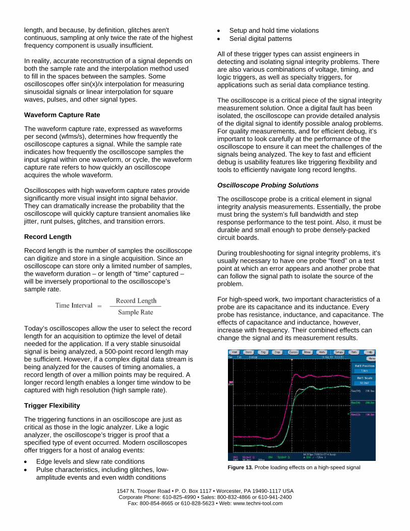
Figure 13. Probe loading effects on a high-speed signal
1547 N. Trooper Road • P. O. Box 1117 • Worcester, PA 19490-1117 USA Corporate Phone: 610-825-4990 • Sales: 800-832-4866 or 610-941-2400
Fax: 800-854-8665 or 610-828-5623 • Web: www.techni-tool.com
Figure 13 demonstrates the probe loading effects on a typical high-speed signal (ground-referenced 250 mV step with about 200 ps rise time). This screen shows the same signal, loaded and unloaded, on a 4 GHz oscilloscope. The addition of the probe has loaded the original signal (the white trace), as shown by the green trace, with the front corner of the step being somewhat slowed. Simply stated, as capacitance and inductance increase, loading on the signal also increases. Similarly, lead length inductance can cause significant distortion in the signal being measured. Probe input characteristics and lead length inductance can actually cause signal integrity problems. A new generation of ultra-low-capacitance oscilloscope probes is the answer to signal integrity and high-speed measurement problems. With wide bandwidths at the probe tip, very short probe tip lead lengths and ultra-low input capacitance, these probes better preserve the signal as it travels to the oscilloscope input. They bring the signal to the acquisition system accurately, with aberrations and all. The probe’s performance is critical because it’s the first link, in a chain of measurement subsystems, that must preserve, capture and display the signal as accurately as possible. A high-bandwidth, low-capacitance probe with both a very short probe tip and ground lead lengths ensures that the bandwidth of the oscilloscope is not wasted. Identifying Signal Integrity Problems with Integrated Measurement Tools In today’s digital systems, with their fast edges and data rates, the analog characteristics underlying digital signals have an ever-increasing impact on system behavior—reliability and repeatability in particular. Efficiently troubleshooting signal integrity problems requires looking at both the analog and digital domains. As mentioned earlier, digital signal deviations can arise from problems in the analog domain like impedance mismatches, transmission line effects, and crosstalk. Similarly, signal deviations may be a by-product of digital issues like setup and hold violations. There is a high degree of interaction between digital and analog signal effects. For devices with just a few digital lines, a mixed signal oscilloscope (MSO) provides both analog and digital measurement capabilities. That enables simultaneous analysis of both domains with one instrument. For more complex devices, with many digital signals, a full-featured logic analyzer integrated with an oscilloscope is the right choice.
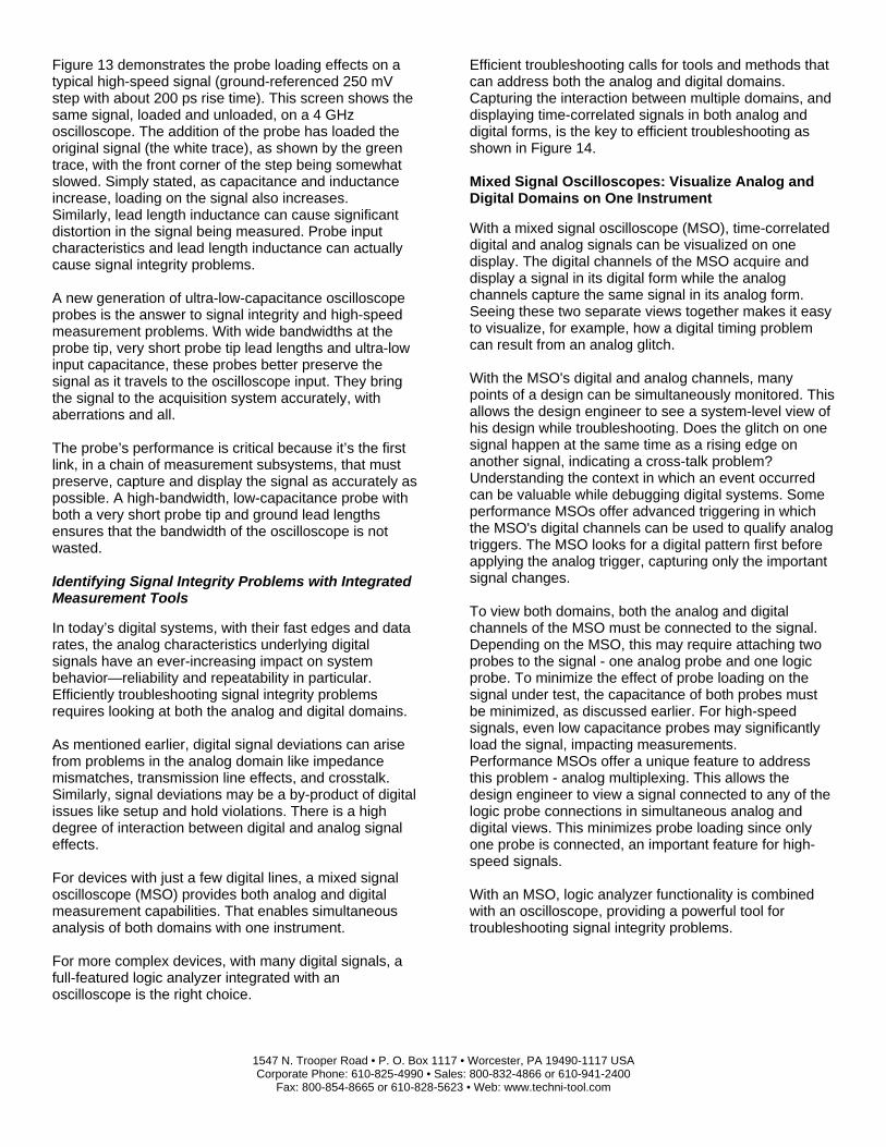
Efficient troubleshooting calls for tools and methods that can address both the analog and digital domains. Capturing the interaction between multiple domains, and displaying time-correlated signals in both analog and digital forms, is the key to efficient troubleshooting as shown in Figure 14. Mixed Signal Oscilloscopes: Visualize Analog and Digital Domains on One Instrument With a mixed signal oscilloscope (MSO), time-correlated digital and analog signals can be visualized on one display. The digital channels of the MSO acquire and display a signal in its digital form while the analog channels capture the same signal in its analog form. Seeing these two separate views together makes it easy to visualize, for example, how a digital timing problem can result from an analog glitch. With the MSO's digital and analog channels, many points of a design can be simultaneously monitored. This allows the design engineer to see a system-level view of his design while troubleshooting. Does the glitch on one signal happen at the same time as a rising edge on another signal, indicating a cross-talk problem? Understanding the context in which an event occurred can be valuable while debugging digital systems. Some performance MSOs offer advanced triggering in which the MSO's digital channels can be used to qualify analog triggers. The MSO looks for a digital pattern first before applying the analog trigger, capturing only the important signal changes. To view both domains, both the analog and digital channels of the MSO must be connected to the signal. Depending on the MSO, this may require attaching two probes to the signal - one analog probe and one logic probe. To minimize the effect of probe loading on the signal under test, the capacitance of both probes must be minimized, as discussed earlier. For high-speed signals, even low capacitance probes may significantly load the signal, impacting measurements. Performance MSOs offer a unique feature to address this problem - analog multiplexing. This allows the design engineer to view a signal connected to any of the logic probe connections in simultaneous analog and digital views. This minimizes probe loading since only one probe is connected, an important feature for high-speed signals. With an MSO, logic analyzer functionality is combined with an oscilloscope, providing a powerful tool for troubleshooting signal integrity problems.
1547 N. Trooper Road • P. O. Box 1117 • Worcester, PA 19490-1117 USA Corporate Phone: 610-825-4990 • Sales: 800-832-4866 or 610-941-2400
Fax: 800-854-8665 or 610-828-5623 • Web: www.techni-tool.com
Figure 14. Crosstalk errors are quickly identified with time-correlated digital and analog measurements on the same display. Revealing the Frequency Domain with Real-Time Spectrum Analyzers For some elusive events, a measurement tool with improved frequency resolution may be required to see subtle frequency events such as clock phase-slip, microphonics, and phase lock loop (PLL) settling. Since a spectrum analyzer provides much greater frequency resolution than an oscilloscope, it can be an invaluable tool for tracking down these events. It is also a good tool for measuring the frequency tolerance of dither generation, which is becoming more common as today’s high-speed clocks are being intentionally dithered for EMI suppression. Since the spectrum analyzer is inherently bandwidth-limited as it is tuned over its frequency range, it also provides excellent dynamic range for measuring low-level signals that may be otherwise masked by noise. Examples include impulse noise, clock glitches from metastable events, and crosstalk signals in the presence of higher amplitude signals. To help detect signal integrity problems, a spectrum analyzer is typically used to determine how frequency and amplitude parameters behave over short and long intervals of time. Common measurement tasks include: • Observing signals masked by noise • Seeing tonal clock signals masked within spread
spectrum signals • Finding and analyzing transient and dynamic signals • Capturing burst transmissions, glitches and
switching transients • Characterizing PLL settling times, frequency drift
and microphonics • Frequency-stepped clock signals • Testing and diagnosing transient EMI effects • Characterizing time-variant modulation schemes • Isolating software and hardware interactions
Traditional swept spectrum analyzers (SA) and vector signal analyzers (VSA) provide snapshots of the signal in the frequency domain or in the modulation domain. But often that's not enough information to confidently describe the dynamic nature of modern signals. Spectrum analyzers are not all equal in their capabilities to see transient events. Each of the measurement tasks listed above involves high-frequency (RF) signals that change over time, often unpredictably. To effectively characterize these signals, engineers need a tool that can discover elusive events, effectively trigger on those events and isolate them into memory so that signal behavior can be analyzed in the frequency, time, modulation, statistical and code domains. DPX Technology: a Revolutionary Tool for Signal Discovery
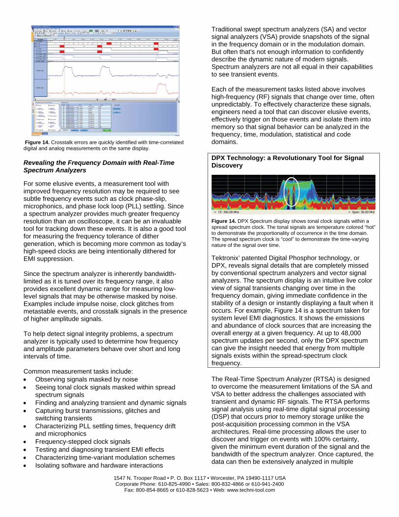
Figure 14. DPX Spectrum display shows tonal clock signals within a spread spectrum clock. The tonal signals are temperature colored “hot” to demonstrate the proportionality of occurrence in the time domain. The spread spectrum clock is “cool” to demonstrate the time-varying nature of the signal over time. Tektronix’ patented Digital Phosphor technology, or DPX, reveals signal details that are completely missed by conventional spectrum analyzers and vector signal analyzers. The spectrum display is an intuitive live color view of signal transients changing over time in the frequency domain, giving immediate confidence in the stability of a design or instantly displaying a fault when it occurs. For example, Figure 14 is a spectrum taken for system level EMI diagnostics. It shows the emissions and abundance of clock sources that are increasing the overall energy at a given frequency. At up to 48,000 spectrum updates per second, only the DPX spectrum can give the insight needed that energy from multiple signals exists within the spread-spectrum clock frequency. The Real-Time Spectrum Analyzer (RTSA) is designed to overcome the measurement limitations of the SA and VSA to better address the challenges associated with transient and dynamic RF signals. The RTSA performs signal analysis using real-time digital signal processing (DSP) that occurs prior to memory storage unlike the post-acquisition processing common in the VSA architectures. Real-time processing allows the user to discover and trigger on events with 100% certainty, given the minimum event duration of the signal and the bandwidth of the spectrum analyzer. Once captured, the data can then be extensively analyzed in multiple
1547 N. Trooper Road • P. O. Box 1117 • Worcester, PA 19490-1117 USA Corporate Phone: 610-825-4990 • Sales: 800-832-4866 or 610-941-2400
Fax: 800-854-8665 or 610-828-5623 • Web: www.techni-tool.com
domains – time, frequency and modulation - using batch processing. With the RTSA’s unique architecture, it is possible to trigger on an event in the frequency domain, capture a continuous time record of changing RF events and perform time-correlated analysis in all domains, speeding troubleshooting of RF signal integrity issues. Since an RTSA must take all of the information contained in a time domain waveform and transform it into frequency domain signals, there are several important signal processing requirements to consider when choosing an RTSA for signal integrity analysis: frequency range, capture bandwidth, sample rate, analysis interval and minimum event duration. Capture Bandwidth and Frequency Range The RTSA’s frequency range and capture bandwidth are critical parameters. It’s important to choose the right RTSA for the signal of interest, with considerations for things like the signal's fundamental frequency, modulation type, frequency spread, and PLL tuning steps. Sample Rate The RTSA’s analog-to-digital converter (ADC) clock rate must be high enough to exceed the Nyquist criteria for the capture bandwidth that's necessary for a particular measurement. Analysis Interval The analysis interval must be long enough to support the narrowest resolution bandwidth of interest when repetitive Fourier transforms are being used to discover, capture and analyze infrequent transient events in the frequency domain. Minimum Event Duration A minimum event is defined as the narrowest, non-repetitive rectangular pulse that can be captured with 100% certainty at the specified accuracy. Narrower events can be detected, but the accuracy and probability may degrade. Minimum event duration will depend largely on the RTSA’s DFT transform rate. For example, an RTSA with a 48,000 spectrums per second DFT transform rate can detect RF pulses as short as 24 microseconds with 100% probability and with full specified accuracy. By comparison, a swept spectrum analyzer with 50 sweeps per second requires pulses longer than 20 milliseconds for 100% probability of detection at full accuracy.
Figure 15. Time-interval error is the difference between the recovered clock and the actual waveform edge. Multi-Domain Analysis An RTSA may be integrated in with a logic analyzer and oscilloscope, allowing the user to trigger in the frequency domain and capture time-correlated frequency (RTSA), time (oscilloscope) and digital (logic analyzer) signals, for in-depth analysis of signal integrity problems. A RTSA is an indispensible tool for detecting and analyzing subtle frequency events that require a measurement tool with tight frequency resolution. Also, its high dynamic range enables the measurement of low-level signals that may otherwise be masked by noise. As designs drive to high-speed data rates, requiring fast timing and techniques like clock dithering, the RTSA will become a critical part of the signal integrity measurement tool set. Simplifying Complex Measurements with Jitter Analysis Tools Signal integrity analysis is not always a matter of finding a slow edge or a low signal amplitude somewhere in the system. As explained earlier, factors like timing jitter can play a large role in system stability. Jitter typically originates in the clock circuitry but can also arise from power supply noise, crosstalk, and PLL circuits. Jitter can affect data, addresses, enable lines and, in fact, virtually any signal in the system. In today’s high-speed designs, as signaling rates climb above 2 GHz and voltage swings shrink to conserve power, the timing jitter in a system becomes a significant percentage of the signaling interval. Under these circumstances, jitter becomes a fundamental performance limit. Understanding what jitter is, and how to characterize it, is the first step to successfully deploy high-speed systems that dependably meet their performance requirements. Conceptually, jitter is the deviation of timing edges from their “correct” locations. In a timing-based system, timing jitter is the most obvious and direct form of non-ideal behavior. As a form of noise, jitter must be treated as a random process and characterized in terms of its statistics. Jitter is divided into two generalized categories: deterministic jitter and random jitter. Deterministic jitter is predictable and consistent, and it has specific causes. Random jitter exhibits a Gaussian distribution which is theoretically unconstrained in amplitude. Since random
1547 N. Trooper Road • P. O. Box 1117 • Worcester, PA 19490-1117 USA Corporate Phone: 610-825-4990 • Sales: 800-832-4866 or 610-941-2400
Fax: 800-854-8665 or 610-828-5623 • Web: www.techni-tool.com
jitter normally fits a Gaussian distribution, certain statistical rules apply. Time-interval error (TIE) is the basis for many jitter measurements. TIE is the difference between the recovered clock (the jitter timing reference) and the actual waveform edge, as shown in Figure 15. Performing histogram and spectrum analysis on the TIE waveform provides the basis for advanced jitter measurements, which is a key step in tracking down the root cause of jitter in the DUT.
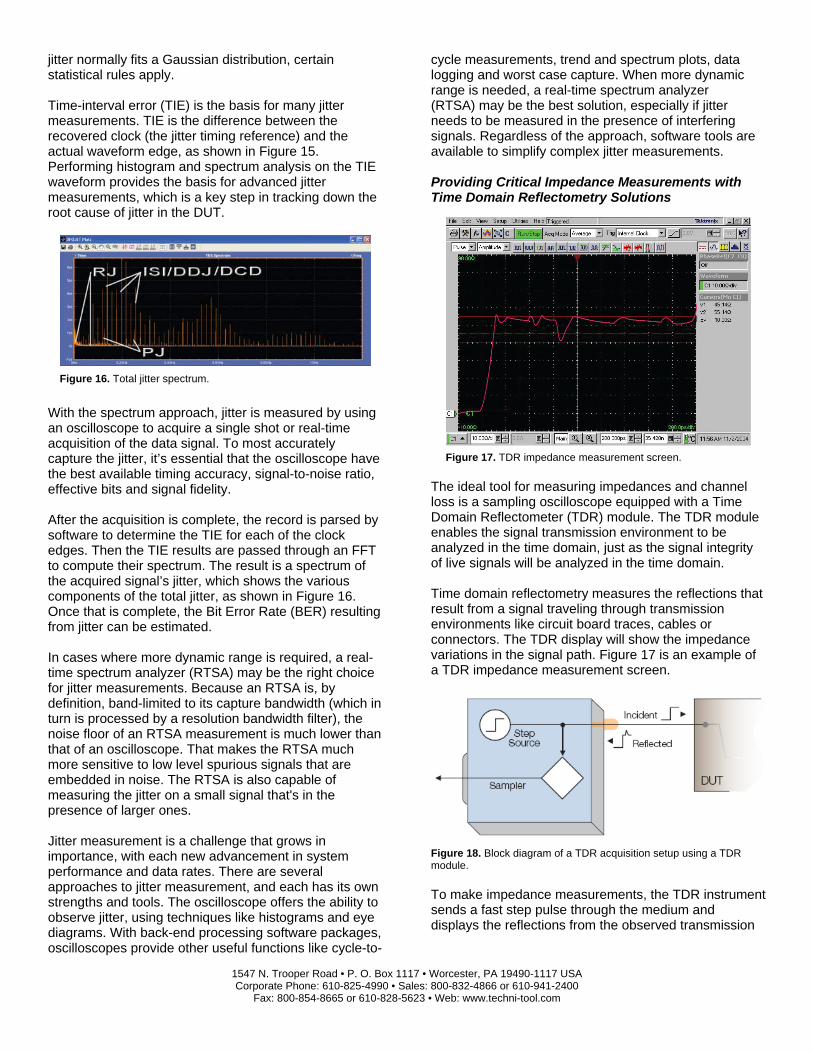
Figure 16. Total jitter spectrum.
With the spectrum approach, jitter is measured by using an oscilloscope to acquire a single shot or real-time acquisition of the data signal. To most accurately capture the jitter, it’s essential that the oscilloscope have the best available timing accuracy, signal-to-noise ratio, effective bits and signal fidelity. After the acquisition is complete, the record is parsed by software to determine the TIE for each of the clock edges. Then the TIE results are passed through an FFT to compute their spectrum. The result is a spectrum of the acquired signal’s jitter, which shows the various components of the total jitter, as shown in Figure 16. Once that is complete, the Bit Error Rate (BER) resulting from jitter can be estimated. In cases where more dynamic range is required, a real-time spectrum analyzer (RTSA) may be the right choice for jitter measurements. Because an RTSA is, by definition, band-limited to its capture bandwidth (which in turn is processed by a resolution bandwidth filter), the noise floor of an RTSA measurement is much lower than that of an oscilloscope. That makes the RTSA much more sensitive to low level spurious signals that are embedded in noise. The RTSA is also capable of measuring the jitter on a small signal that's in the presence of larger ones. Jitter measurement is a challenge that grows in importance, with each new advancement in system performance and data rates. There are several approaches to jitter measurement, and each has its own strengths and tools. The oscilloscope offers the ability to observe jitter, using techniques like histograms and eye diagrams. With back-end processing software packages, oscilloscopes provide other useful functions like cycle-to-
cycle measurements, trend and spectrum plots, data logging and worst case capture. When more dynamic range is needed, a real-time spectrum analyzer (RTSA) may be the best solution, especially if jitter needs to be measured in the presence of interfering signals. Regardless of the approach, software tools are available to simplify complex jitter measurements. Providing Critical Impedance Measurements with Time Domain Reflectometry Solutions
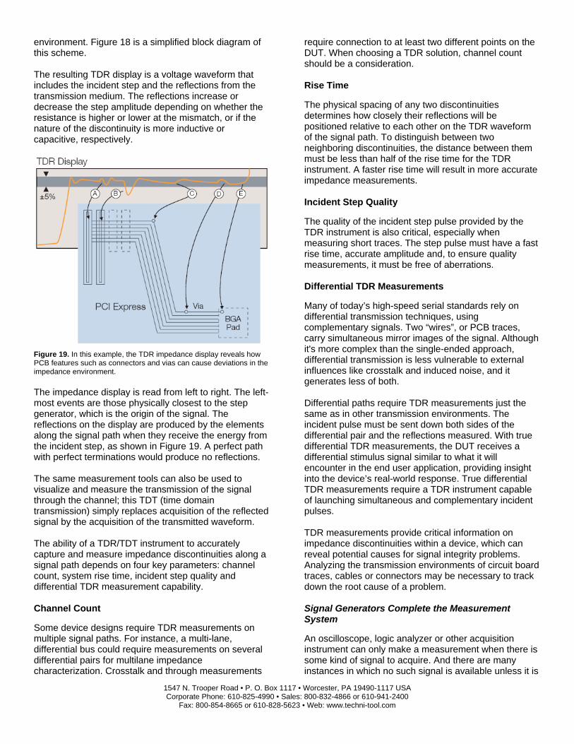
Figure 17. TDR impedance measurement screen. The ideal tool for measuring impedances and channel loss is a sampling oscilloscope equipped with a Time Domain Reflectometer (TDR) module. The TDR module enables the signal transmission environment to be analyzed in the time domain, just as the signal integrity of live signals will be analyzed in the time domain. Time domain reflectometry measures the reflections that result from a signal traveling through transmission environments like circuit board traces, cables or connectors. The TDR display will show the impedance variations in the signal path. Figure 17 is an example of a TDR impedance measurement screen.
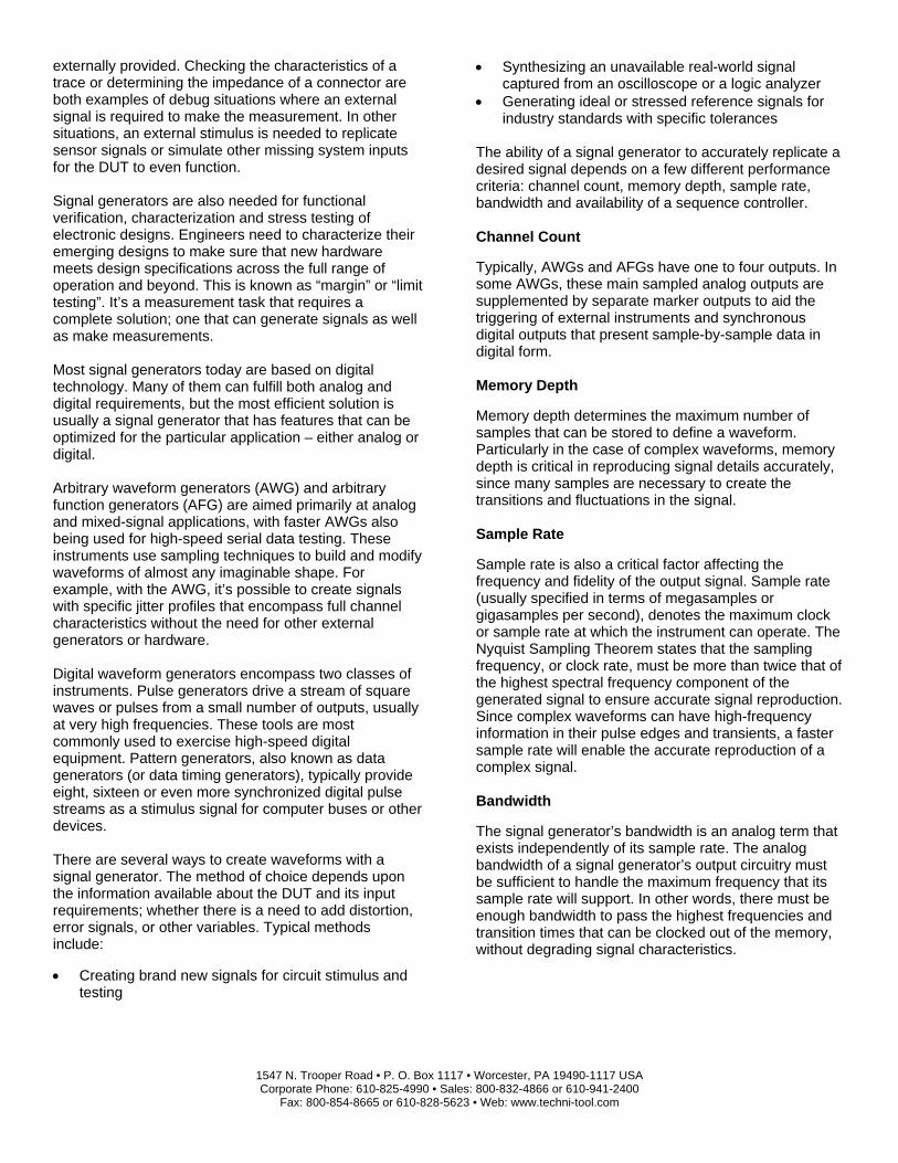
Figure 18. Block diagram of a TDR acquisition setup using a TDR module. To make impedance measurements, the TDR instrument sends a fast step pulse through the medium and displays the reflections from the observed transmission
1547 N. Trooper Road • P. O. Box 1117 • Worcester, PA 19490-1117 USA Corporate Phone: 610-825-4990 • Sales: 800-832-4866 or 610-941-2400
Fax: 800-854-8665 or 610-828-5623 • Web: www.techni-tool.com
environment. Figure 18 is a simplified block diagram of this scheme. The resulting TDR display is a voltage waveform that includes the incident step and the reflections from the transmission medium. The reflections increase or decrease the step amplitude depending on whether the resistance is higher or lower at the mismatch, or if the nature of the discontinuity is more inductive or capacitive, respectively.
Figure 19. In this example, the TDR impedance display reveals how PCB features such as connectors and vias can cause deviations in the impedance environment. The impedance display is read from left to right. The left-most events are those physically closest to the step generator, which is the origin of the signal. The reflections on the display are produced by the elements along the signal path when they receive the energy from the incident step, as shown in Figure 19. A perfect path with perfect terminations would produce no reflections. The same measurement tools can also be used to visualize and measure the transmission of the signal through the channel; this TDT (time domain transmission) simply replaces acquisition of the reflected signal by the acquisition of the transmitted waveform. The ability of a TDR/TDT instrument to accurately capture and measure impedance discontinuities along a signal path depends on four key parameters: channel count, system rise time, incident step quality and differential TDR measurement capability. Channel Count Some device designs require TDR measurements on multiple signal paths. For instance, a multi-lane, differential bus could require measurements on several differential pairs for multilane impedance characterization. Crosstalk and through measurements
require connection to at least two different points on the DUT. When choosing a TDR solution, channel count should be a consideration. Rise Time The physical spacing of any two discontinuities determines how closely their reflections will be positioned relative to each other on the TDR waveform of the signal path. To distinguish between two neighboring discontinuities, the distance between them must be less than half of the rise time for the TDR instrument. A faster rise time will result in more accurate impedance measurements. Incident Step Quality The quality of the incident step pulse provided by the TDR instrument is also critical, especially when measuring short traces. The step pulse must have a fast rise time, accurate amplitude and, to ensure quality measurements, it must be free of aberrations. Differential TDR Measurements Many of today’s high-speed serial standards rely on differential transmission techniques, using complementary signals. Two “wires”, or PCB traces, carry simultaneous mirror images of the signal. Although it's more complex than the single-ended approach, differential transmission is less vulnerable to external influences like crosstalk and induced noise, and it generates less of both. Differential paths require TDR measurements just the same as in other transmission environments. The incident pulse must be sent down both sides of the differential pair and the reflections measured. With true differential TDR measurements, the DUT receives a differential stimulus signal similar to what it will encounter in the end user application, providing insight into the device’s real-world response. True differential TDR measurements require a TDR instrument capable of launching simultaneous and complementary incident pulses. TDR measurements provide critical information on impedance discontinuities within a device, which can reveal potential causes for signal integrity problems. Analyzing the transmission environments of circuit board traces, cables or connectors may be necessary to track down the root cause of a problem. Signal Generators Complete the Measurement System An oscilloscope, logic analyzer or other acquisition instrument can only make a measurement when there is some kind of signal to acquire. And there are many instances in which no such signal is available unless it is
1547 N. Trooper Road • P. O. Box 1117 • Worcester, PA 19490-1117 USA Corporate Phone: 610-825-4990 • Sales: 800-832-4866 or 610-941-2400
Fax: 800-854-8665 or 610-828-5623 • Web: www.techni-tool.com
externally provided. Checking the characteristics of a trace or determining the impedance of a connector are both examples of debug situations where an external signal is required to make the measurement. In other situations, an external stimulus is needed to replicate sensor signals or simulate other missing system inputs for the DUT to even function. Signal generators are also needed for functional verification, characterization and stress testing of electronic designs. Engineers need to characterize their emerging designs to make sure that new hardware meets design specifications across the full range of operation and beyond. This is known as “margin” or “limit testing”. It’s a measurement task that requires a complete solution; one that can generate signals as well as make measurements. Most signal generators today are based on digital technology. Many of them can fulfill both analog and digital requirements, but the most efficient solution is usually a signal generator that has features that can be optimized for the particular application – either analog or digital. Arbitrary waveform generators (AWG) and arbitrary function generators (AFG) are aimed primarily at analog and mixed-signal applications, with faster AWGs also being used for high-speed serial data testing. These instruments use sampling techniques to build and modify waveforms of almost any imaginable shape. For example, with the AWG, it’s possible to create signals with specific jitter profiles that encompass full channel characteristics without the need for other external generators or hardware. Digital waveform generators encompass two classes of instruments. Pulse generators drive a stream of square waves or pulses from a small number of outputs, usually at very high frequencies. These tools are most commonly used to exercise high-speed digital equipment. Pattern generators, also known as data generators (or data timing generators), typically provide eight, sixteen or even more synchronized digital pulse streams as a stimulus signal for computer buses or other devices. There are several ways to create waveforms with a signal generator. The method of choice depends upon the information available about the DUT and its input requirements; whether there is a need to add distortion, error signals, or other variables. Typical methods include: • Creating brand new signals for circuit stimulus and
testing
• Synthesizing an unavailable real-world signal captured from an oscilloscope or a logic analyzer
• Generating ideal or stressed reference signals for industry standards with specific tolerances
The ability of a signal generator to accurately replicate a desired signal depends on a few different performance criteria: channel count, memory depth, sample rate, bandwidth and availability of a sequence controller. Channel Count Typically, AWGs and AFGs have one to four outputs. In some AWGs, these main sampled analog outputs are supplemented by separate marker outputs to aid the triggering of external instruments and synchronous digital outputs that present sample-by-sample data in digital form. Memory Depth Memory depth determines the maximum number of samples that can be stored to define a waveform. Particularly in the case of complex waveforms, memory depth is critical in reproducing signal details accurately, since many samples are necessary to create the transitions and fluctuations in the signal. Sample Rate Sample rate is also a critical factor affecting the frequency and fidelity of the output signal. Sample rate (usually specified in terms of megasamples or gigasamples per second), denotes the maximum clock or sample rate at which the instrument can operate. The Nyquist Sampling Theorem states that the sampling frequency, or clock rate, must be more than twice that of the highest spectral frequency component of the generated signal to ensure accurate signal reproduction. Since complex waveforms can have high-frequency information in their pulse edges and transients, a faster sample rate will enable the accurate reproduction of a complex signal. Bandwidth The signal generator’s bandwidth is an analog term that exists independently of its sample rate. The analog bandwidth of a signal generator’s output circuitry must be sufficient to handle the maximum frequency that its sample rate will support. In other words, there must be enough bandwidth to pass the highest frequencies and transition times that can be clocked out of the memory, without degrading signal characteristics.
1547 N. Trooper Road • P. O. Box 1117 • Worcester, PA 19490-1117 USA Corporate Phone: 610-825-4990 • Sales: 800-832-4866 or 610-941-2400
Fax: 800-854-8665 or 610-828-5623 • Web: www.techni-tool.com
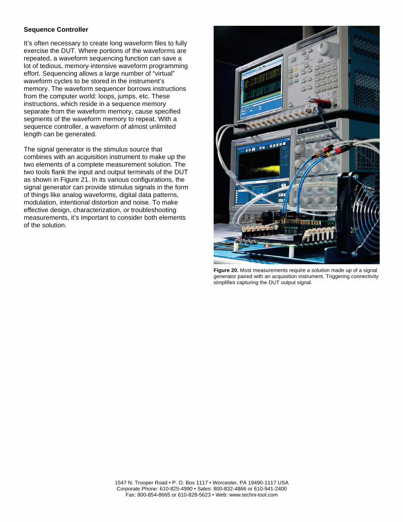
Sequence Controller It’s often necessary to create long waveform files to fully exercise the DUT. Where portions of the waveforms are repeated, a waveform sequencing function can save a lot of tedious, memory-intensive waveform programming effort. Sequencing allows a large number of “virtual” waveform cycles to be stored in the instrument’s memory. The waveform sequencer borrows instructions from the computer world: loops, jumps, etc. These instructions, which reside in a sequence memory separate from the waveform memory, cause specified segments of the waveform memory to repeat. With a sequence controller, a waveform of almost unlimited length can be generated. The signal generator is the stimulus source that combines with an acquisition instrument to make up the two elements of a complete measurement solution. The two tools flank the input and output terminals of the DUT as shown in Figure 21. In its various configurations, the signal generator can provide stimulus signals in the form of things like analog waveforms, digital data patterns, modulation, intentional distortion and noise. To make effective design, characterization, or troubleshooting measurements, it’s important to consider both elements of the solution.
Figure 20. Most measurements require a solution made up of a signal generator paired with an acquisition instrument. Triggering connectivity simplifies capturing the DUT output signal.
1547 N. Trooper Road • P. O. Box 1117 • Worcester, PA 19490-1117 USA Corporate Phone: 610-825-4990 • Sales: 800-832-4866 or 610-941-2400
Fax: 800-854-8665 or 610-828-5623 • Web: www.techni-tool.com
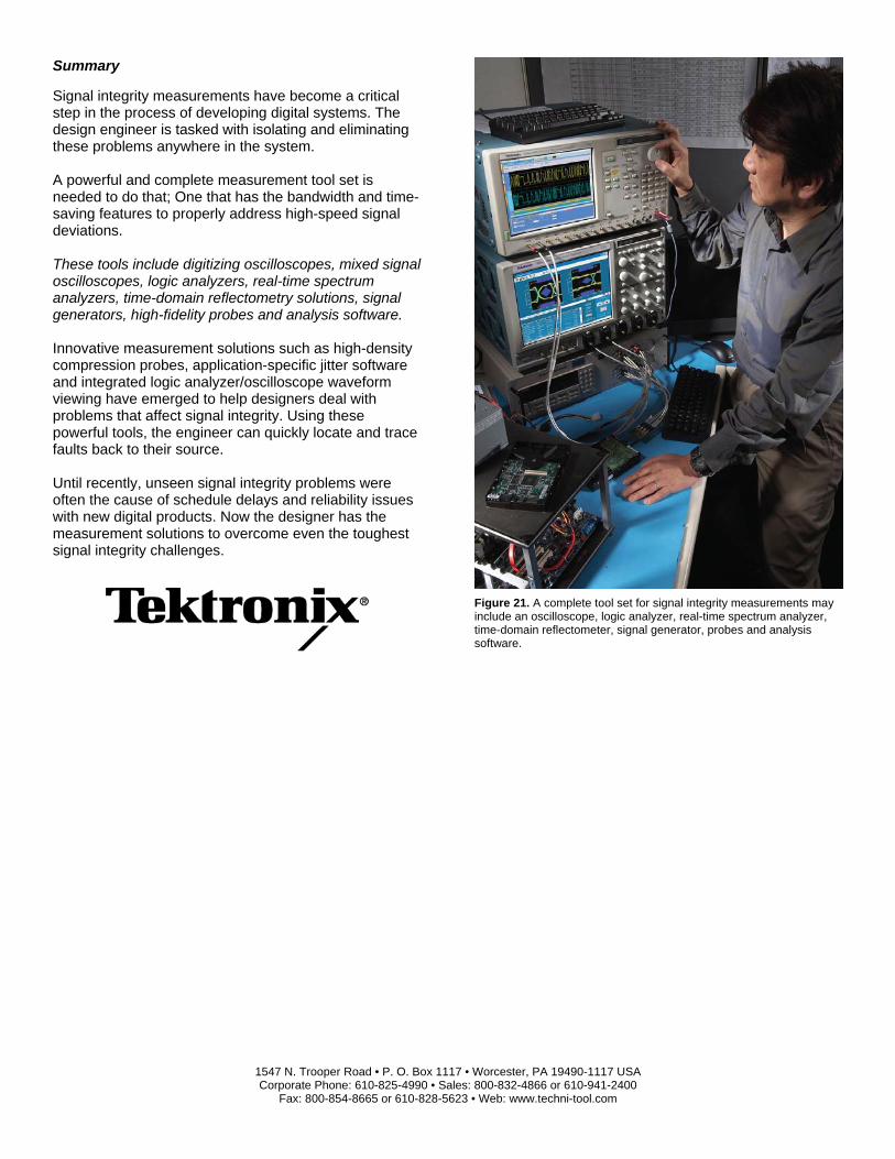
Summary Signal integrity measurements have become a critical step in the process of developing digital systems. The design engineer is tasked with isolating and eliminating these problems anywhere in the system. A powerful and complete measurement tool set is needed to do that; One that has the bandwidth and time-saving features to properly address high-speed signal deviations. These tools include digitizing oscilloscopes, mixed signal oscilloscopes, logic analyzers, real-time spectrum analyzers, time-domain reflectometry solutions, signal generators, high-fidelity probes and analysis software. Innovative measurement solutions such as high-density compression probes, application-specific jitter software and integrated logic analyzer/oscilloscope waveform viewing have emerged to help designers deal with problems that affect signal integrity. Using these powerful tools, the engineer can quickly locate and trace faults back to their source. Until recently, unseen signal integrity problems were often the cause of schedule delays and reliability issues with new digital products. Now the designer has the measurement solutions to overcome even the toughest signal integrity challenges.
Figure 21. A complete tool set for signal integrity measurements may include an oscilloscope, logic analyzer, real-time spectrum analyzer, time-domain reflectometer, signal generator, probes and analysis software.