Research Article Engineering Change Orders Design Using...
6
Research Article Engineering Change Orders Design Using Multiple Variables Linear Programming for VLSI Design Yu-Cheng Fan, Chih-Kang Lin, Shih-Ying Chou, Chun-Hung Wang, Shu-Hsien Wu, and Hung-Kuan Liu Department of Electronic Engineering, National Taipei University of Technology, Taipei 10608, Taiwan Correspondence should be addressed to Yu-Cheng Fan; [email protected] Received 7 June 2014; Accepted 18 July 2014; Published 24 August 2014 Academic Editor: Chih-Cheng Lu Copyright © 2014 Yu-Cheng Fan et al. is is an open access article distributed under the Creative Commons Attribution License, which permits unrestricted use, distribution, and reproduction in any medium, provided the original work is properly cited. An engineering change orders design using multiple variable linear programming for VLSI design is presented in this paper. is approach addresses the main issues of resource between spare cells and target cells. We adopt linear programming technique to plan and balance the spare cells and target cells to meet the new specification according to logic transformation. e proposed method solves the related problem of resource for ECO problems and provides a well solution. e scheme shows new concept to manage the spare cells to meet possible target cells for ECO research. 1. Introduction Engineering change orders (ECO) are important technolo- gies used for changes in integrated circuit (IC) layout and compensate for design problems. Traditionally, when chip shows errors, it oſten requires new photomasks for all layers. However, photomasks of deep-submicron semiconductor fabrication process are very expensive. In order to save money, ECO technology modifies only a few of the metal layers (metal-mask ECO) to reduce the cost of photomasks for all layers [1]. To perform the ECO, IC designers adopt sprinkling many unused logic gates during IC design flow. When chip is manufactured and shows design errors, IC designers modify the gate-level net-list using the presprinkling unused logic gates. At the same time, the designers track and verify the modification to check formal equivalence aſter ECO process. e designers must guarantee the revised design matching the revised specification. How to achieve ECO efficiently? ere are some litera- tures that address this problem and provide related solution. In literature [2], Tan and Jiang describe a typical metal- only ECO flow with four steps that include placement and spare cell distribution, logic difference extraction, metal-only ECO synthesis, and ECO routing [2]. Kuo et al. insert spare cells with constant insertion for engineering change and describe an iterative method to determine feasible mapping solutions for an EC problem [3]. Besides, in order to per- form ECO efficiently, literature [4–9] adopt minimal change EC equations automatically. Brand proposed incremental synthesis method [4]. Huang presented a hybrid tool for automatic logic rectification [5]. Lin et al. addressed logic synthesis techniques for engineering change problems [6]. Shinsha et al. performed incremental logic synthesis through gate logic structure identification [7]. Swamy et al. achieved minimal logic resynthesis for engineering change [8]. Watan- abe and Brayton presented another kind of incremental synthesis technique for engineering changes [9]. However, few researchers discuss the resource between spare cells and target cells. erefore, in order to solve the problems, we adopt linear programming technique to plan and balance the spare cells and target cells in this paper. e proposed scheme meets the new specification according to logic transformation and overcomes the related problems of resource for ECO research. is paper is organized as follows. In Section 2, we address typical ECO design flow. In Section 3, logic trans- formation is discussed. In Section 4, multiple variables linear Hindawi Publishing Corporation VLSI Design Volume 2014, Article ID 698041, 5 pages http://dx.doi.org/10.1155/2014/698041
Transcript of Research Article Engineering Change Orders Design Using...

Research ArticleEngineering Change Orders Design Using Multiple VariablesLinear Programming for VLSI Design
Yu-Cheng Fan Chih-Kang Lin Shih-Ying Chou Chun-Hung WangShu-Hsien Wu and Hung-Kuan Liu
Department of Electronic Engineering National Taipei University of Technology Taipei 10608 Taiwan
Correspondence should be addressed to Yu-Cheng Fan skystarntutedutw
Received 7 June 2014 Accepted 18 July 2014 Published 24 August 2014
Academic Editor Chih-Cheng Lu
Copyright copy 2014 Yu-Cheng Fan et al This is an open access article distributed under the Creative Commons Attribution Licensewhich permits unrestricted use distribution and reproduction in any medium provided the original work is properly cited
An engineering change orders design using multiple variable linear programming for VLSI design is presented in this paper Thisapproach addresses themain issues of resource between spare cells and target cellsWe adopt linear programming technique to planand balance the spare cells and target cells to meet the new specification according to logic transformation The proposed methodsolves the related problem of resource for ECO problems and provides a well solution The scheme shows new concept to managethe spare cells to meet possible target cells for ECO research
1 Introduction
Engineering change orders (ECO) are important technolo-gies used for changes in integrated circuit (IC) layout andcompensate for design problems Traditionally when chipshows errors it often requires new photomasks for all layersHowever photomasks of deep-submicron semiconductorfabrication process are very expensive In order to savemoney ECO technology modifies only a few of the metallayers (metal-mask ECO) to reduce the cost of photomasksfor all layers [1]
To perform the ECO IC designers adopt sprinklingmanyunused logic gates during IC design flow When chip ismanufactured and shows design errors IC designers modifythe gate-level net-list using the presprinkling unused logicgates At the same time the designers track and verify themodification to check formal equivalence after ECO processThe designers must guarantee the revised design matchingthe revised specification
How to achieve ECO efficiently There are some litera-tures that address this problem and provide related solutionIn literature [2] Tan and Jiang describe a typical metal-only ECO flow with four steps that include placement andspare cell distribution logic difference extraction metal-only
ECO synthesis and ECO routing [2] Kuo et al insert sparecells with constant insertion for engineering change anddescribe an iterative method to determine feasible mappingsolutions for an EC problem [3] Besides in order to per-form ECO efficiently literature [4ndash9] adopt minimal changeEC equations automatically Brand proposed incrementalsynthesis method [4] Huang presented a hybrid tool forautomatic logic rectification [5] Lin et al addressed logicsynthesis techniques for engineering change problems [6]Shinsha et al performed incremental logic synthesis throughgate logic structure identification [7] Swamy et al achievedminimal logic resynthesis for engineering change [8]Watan-abe and Brayton presented another kind of incrementalsynthesis technique for engineering changes [9] Howeverfew researchers discuss the resource between spare cells andtarget cells Therefore in order to solve the problems weadopt linear programming technique to plan and balance thespare cells and target cells in this paperThe proposed schememeets the new specification according to logic transformationand overcomes the related problems of resource for ECOresearch
This paper is organized as follows In Section 2 weaddress typical ECO design flow In Section 3 logic trans-formation is discussed In Section 4 multiple variables linear
Hindawi Publishing CorporationVLSI DesignVolume 2014 Article ID 698041 5 pageshttpdxdoiorg1011552014698041
2 VLSI Design
Old net-listECONew registertransfer level
ECO New net-list
ECO editing
Old registertransfer level
Logic synthesis DFT Placement
and routing
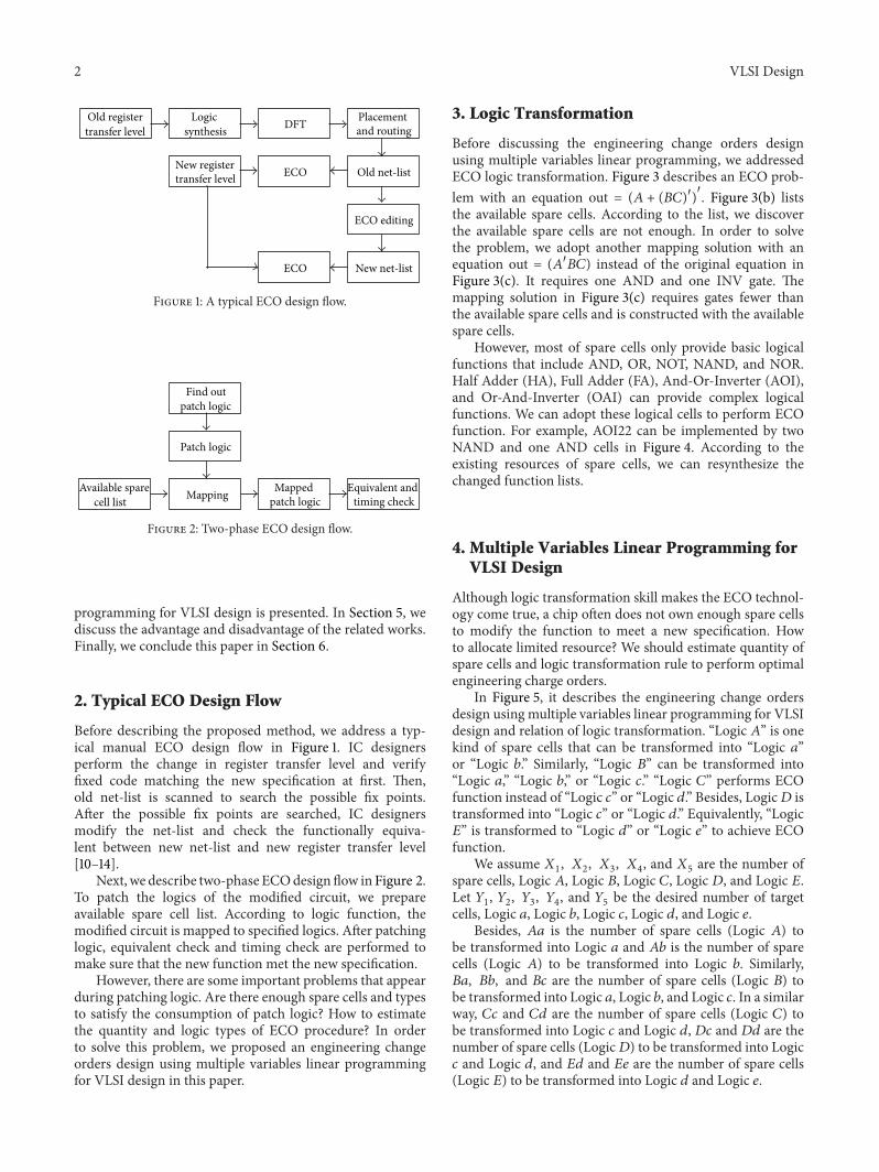
Figure 1 A typical ECO design flow
Find out patch logic
Mapped patch logic
Patch logic
MappingAvailable spare cell list
Equivalent and timing check
Figure 2 Two-phase ECO design flow
programming for VLSI design is presented In Section 5 wediscuss the advantage and disadvantage of the related worksFinally we conclude this paper in Section 6
2 Typical ECO Design Flow
Before describing the proposed method we address a typ-ical manual ECO design flow in Figure 1 IC designersperform the change in register transfer level and verifyfixed code matching the new specification at first Thenold net-list is scanned to search the possible fix pointsAfter the possible fix points are searched IC designersmodify the net-list and check the functionally equiva-lent between new net-list and new register transfer level[10ndash14]
Next we describe two-phase ECOdesign flow in Figure 2To patch the logics of the modified circuit we prepareavailable spare cell list According to logic function themodified circuit is mapped to specified logics After patchinglogic equivalent check and timing check are performed tomake sure that the new function met the new specification
However there are some important problems that appearduring patching logic Are there enough spare cells and typesto satisfy the consumption of patch logic How to estimatethe quantity and logic types of ECO procedure In orderto solve this problem we proposed an engineering changeorders design using multiple variables linear programmingfor VLSI design in this paper
3 Logic Transformation
Before discussing the engineering change orders designusing multiple variables linear programming we addressedECO logic transformation Figure 3 describes an ECO prob-lem with an equation out = (119860 + (119861119862)1015840)1015840 Figure 3(b) liststhe available spare cells According to the list we discoverthe available spare cells are not enough In order to solvethe problem we adopt another mapping solution with anequation out = (1198601015840119861119862) instead of the original equation inFigure 3(c) It requires one AND and one INV gate Themapping solution in Figure 3(c) requires gates fewer thanthe available spare cells and is constructed with the availablespare cells
However most of spare cells only provide basic logicalfunctions that include AND OR NOT NAND and NORHalf Adder (HA) Full Adder (FA) And-Or-Inverter (AOI)and Or-And-Inverter (OAI) can provide complex logicalfunctions We can adopt these logical cells to perform ECOfunction For example AOI22 can be implemented by twoNAND and one AND cells in Figure 4 According to theexisting resources of spare cells we can resynthesize thechanged function lists
4 Multiple Variables Linear Programming forVLSI Design
Although logic transformation skill makes the ECO technol-ogy come true a chip often does not own enough spare cellsto modify the function to meet a new specification Howto allocate limited resource We should estimate quantity ofspare cells and logic transformation rule to perform optimalengineering charge orders
In Figure 5 it describes the engineering change ordersdesign using multiple variables linear programming for VLSIdesign and relation of logic transformation ldquoLogic 119860rdquo is onekind of spare cells that can be transformed into ldquoLogic 119886rdquoor ldquoLogic 119887rdquo Similarly ldquoLogic 119861rdquo can be transformed intoldquoLogic 119886rdquo ldquoLogic 119887rdquo or ldquoLogic 119888rdquo ldquoLogic 119862rdquo performs ECOfunction instead of ldquoLogic 119888rdquo or ldquoLogic 119889rdquo Besides Logic119863 istransformed into ldquoLogic 119888rdquo or ldquoLogic 119889rdquo Equivalently ldquoLogic119864rdquo is transformed to ldquoLogic 119889rdquo or ldquoLogic 119890rdquo to achieve ECOfunction
We assume 1198831 1198832 1198833 1198834 and 119883
5are the number of
spare cells Logic 119860 Logic 119861 Logic 119862 Logic 119863 and Logic 119864Let 1198841 1198842 1198843 1198844 and 119884
5be the desired number of target
cells Logic 119886 Logic 119887 Logic 119888 Logic 119889 and Logic 119890Besides 119860119886 is the number of spare cells (Logic 119860) to
be transformed into Logic 119886 and 119860119887 is the number of sparecells (Logic 119860) to be transformed into Logic 119887 Similarly119861119886 119861119887 and 119861119888 are the number of spare cells (Logic 119861) tobe transformed into Logic 119886 Logic 119887 and Logic 119888 In a similarway 119862119888 and 119862119889 are the number of spare cells (Logic 119862) tobe transformed into Logic 119888 and Logic 119889 119863119888 and 119863119889 are thenumber of spare cells (Logic119863) to be transformed into Logic119888 and Logic 119889 and 119864119889 and 119864119890 are the number of spare cells(Logic 119864) to be transformed into Logic 119889 and Logic 119890
VLSI Design 3
A
A
B
C
BC
(a)
Type Spare cellsAND 2OR 2INV 1
NAND 1
(b)
A
B
C
A
(c)
Figure 3 Example of an ECO problem (a) EC equation output = (119860 + (119861119862)1015840)1015840 (b) Spare cells (c) Mapping output = (1198601015840119861119862)
(a) (b)
Figure 4 AOI22 can be implemented by two NAND and one AND cells
X1
Y1
X2
Y2
X3
Y3
X4
Y4
X5
Y5
Logic A
Logic B
Logic C
Logic D
Logic E
Logic a
Logic b
Logic c
Logic d
Logic e
Aa
Ab
Ba
Bb
Bc
Cc
Cd
Dc
Dd
Ed
Ee
Figure 5 ECO design using multiple variables linear programmingfor VLSI design and relation of logic transformation
Therefore the restriction rule of the number of spare cellsand transformed target cells in Figure 5 is written as follows
1198831= 119860119886 + 119860119887
1198832= 119861119886 + 119861119887 + 119861119888
1198833= 119862119888 + 119862119889
1198834= 119863119888 + 119863119889
1198835= 119864119889 + 119864119890
(1)
Besides the restriction rule of the engineering changeorders design usingmultiple variables linear programming inFigure 5 is written as follows
119860119886 + 119861119886 ≧ 1198841 (2)
119860119887 + 119861119887 ≧ 1198842 (3)
119861119888 + 119862119888 + 119863119888 ≧ 1198843 (4)
119862119889 + 119863119889 + 119864119889 ≧ 1198844 (5)
119864119889 + 119864119890 ≧ 1198845 (6)
However spare cells are not often enough designershould balance the spare cell allocation to meet all require-ments of desirable cells
We assume one case when 119861119887 ≦ 1198842 In order to provide
enough spare cells we should increase the number of 119860119887 toachieve 119860119887 + 119861119887 ≧ 119884
2
Similarly when 119862119888 + 119863119888 ≦ 1198843 we should increase 119861119888
number to meet 119861119888 + 119862119888 + 119863119888 ≧ 1198843
Therefore we define another restriction rule of the engi-neering change orders design which is written as follows
119860119886 = 1198831minus 119860119887
119861119886 = 1198832minus 119861119887 minus 119861119888
(7)
4 VLSI Design
Table 1 ECO methods comparison
Method Traditional ECO Proposed methodCell resource prediction Constraint based Multiple variables linear programmingPredictive precision of patching logic number Normal precision High precisionBalance between spare cells and target cells Low balance High balanceRestriction rule Not define DefineResource optimization Not define DefineSolution boundary Not define Define
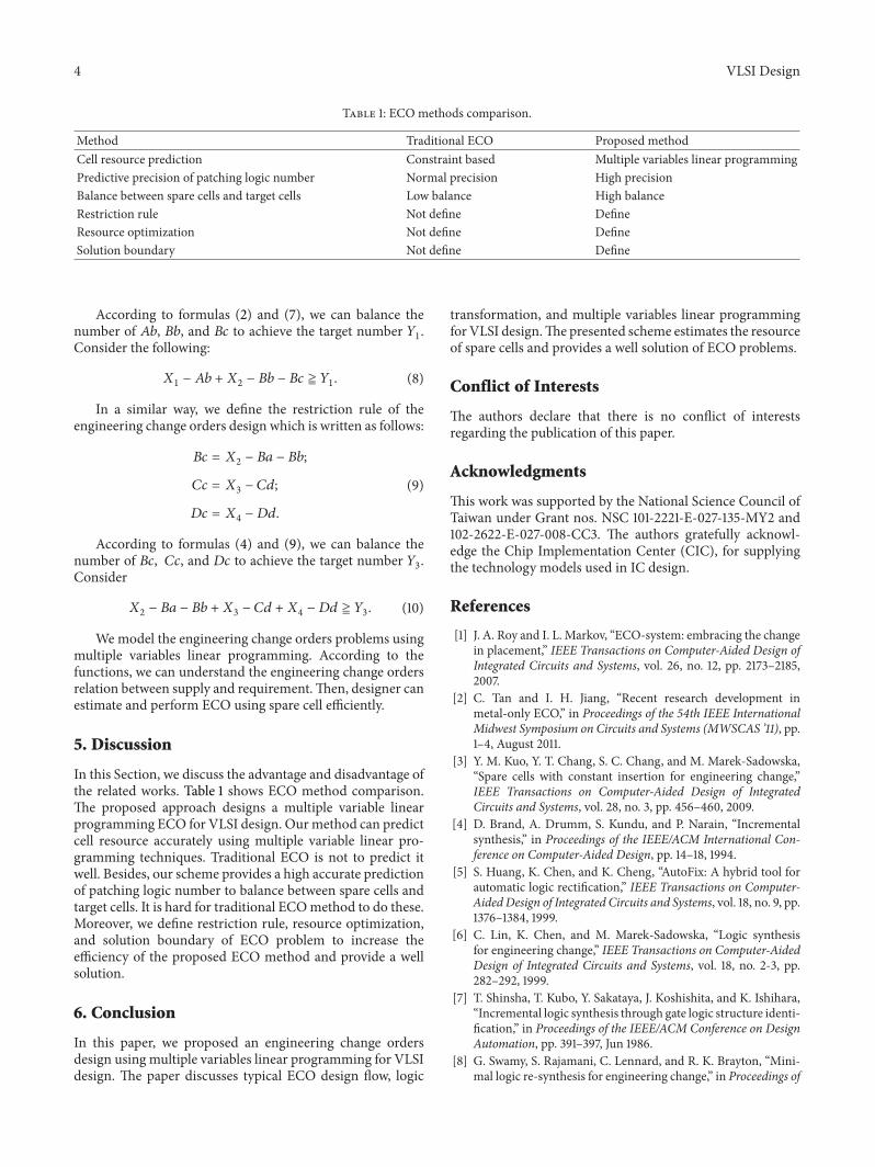
According to formulas (2) and (7) we can balance thenumber of 119860119887 119861119887 and 119861119888 to achieve the target number 119884
1
Consider the following
1198831minus 119860119887 + 119883
2minus 119861119887 minus 119861119888 ≧ 119884
1 (8)
In a similar way we define the restriction rule of theengineering change orders design which is written as follows
119861119888 = 1198832minus 119861119886 minus 119861119887
119862119888 = 1198833minus 119862119889
119863119888 = 1198834minus 119863119889
(9)
According to formulas (4) and (9) we can balance thenumber of 119861119888 119862119888 and 119863119888 to achieve the target number 119884
3
Consider
1198832minus 119861119886 minus 119861119887 + 119883
3minus 119862119889 + 119883
4minus 119863119889 ≧ 119884
3 (10)
We model the engineering change orders problems usingmultiple variables linear programming According to thefunctions we can understand the engineering change ordersrelation between supply and requirementThen designer canestimate and perform ECO using spare cell efficiently
5 Discussion
In this Section we discuss the advantage and disadvantage ofthe related works Table 1 shows ECO method comparisonThe proposed approach designs a multiple variable linearprogramming ECO for VLSI design Ourmethod can predictcell resource accurately using multiple variable linear pro-gramming techniques Traditional ECO is not to predict itwell Besides our scheme provides a high accurate predictionof patching logic number to balance between spare cells andtarget cells It is hard for traditional ECOmethod to do theseMoreover we define restriction rule resource optimizationand solution boundary of ECO problem to increase theefficiency of the proposed ECO method and provide a wellsolution
6 Conclusion
In this paper we proposed an engineering change ordersdesign using multiple variables linear programming for VLSIdesign The paper discusses typical ECO design flow logic
transformation and multiple variables linear programmingfor VLSI designThe presented scheme estimates the resourceof spare cells and provides a well solution of ECO problems
Conflict of Interests
The authors declare that there is no conflict of interestsregarding the publication of this paper
Acknowledgments
This work was supported by the National Science Council ofTaiwan under Grant nos NSC 101-2221-E-027-135-MY2 and102-2622-E-027-008-CC3 The authors gratefully acknowl-edge the Chip Implementation Center (CIC) for supplyingthe technology models used in IC design
References
[1] J A Roy and I L Markov ldquoECO-system embracing the changein placementrdquo IEEE Transactions on Computer-Aided Design ofIntegrated Circuits and Systems vol 26 no 12 pp 2173ndash21852007
[2] C Tan and I H Jiang ldquoRecent research development inmetal-only ECOrdquo in Proceedings of the 54th IEEE InternationalMidwest Symposium on Circuits and Systems (MWSCAS rsquo11) pp1ndash4 August 2011
[3] Y M Kuo Y T Chang S C Chang and M Marek-SadowskaldquoSpare cells with constant insertion for engineering changerdquoIEEE Transactions on Computer-Aided Design of IntegratedCircuits and Systems vol 28 no 3 pp 456ndash460 2009
[4] D Brand A Drumm S Kundu and P Narain ldquoIncrementalsynthesisrdquo in Proceedings of the IEEEACM International Con-ference on Computer-Aided Design pp 14ndash18 1994
[5] S Huang K Chen and K Cheng ldquoAutoFix A hybrid tool forautomatic logic rectificationrdquo IEEE Transactions on Computer-Aided Design of Integrated Circuits and Systems vol 18 no 9 pp1376ndash1384 1999
[6] C Lin K Chen and M Marek-Sadowska ldquoLogic synthesisfor engineering changerdquo IEEE Transactions on Computer-AidedDesign of Integrated Circuits and Systems vol 18 no 2-3 pp282ndash292 1999
[7] T Shinsha T Kubo Y Sakataya J Koshishita and K IshiharaldquoIncremental logic synthesis through gate logic structure identi-ficationrdquo in Proceedings of the IEEEACM Conference on DesignAutomation pp 391ndash397 Jun 1986
[8] G Swamy S Rajamani C Lennard and R K Brayton ldquoMini-mal logic re-synthesis for engineering changerdquo in Proceedings of
VLSI Design 5
the IEEE International Symposium on Circuits and Systems pp1596ndash1599 1997
[9] Y Watanabe and R K Brayton ldquoIncremental synthesis forengineering changesrdquo in Proceedings of the IEEE InternationalConference on Computer Design VLSI in Computers and Pro-cessors (ICCD rsquo91) pp 40ndash43 Cambridge Mass USA October1991
[10] J Wang Finding the Minimal Logic Difference for FunctionalECO Taiwan Cadence Design Systems 2012
[11] Y C Fan and H W Tsao ldquoWatermarking for intellectualproperty protectionrdquo IEE Electronics Letters vol 39 no 18 pp1316ndash1318 2003
[12] Y Fan and H Tsao ldquoBoundary scan test scheme for IPcore identification via watermarkingrdquo IEICE Transactions onInformation and Systems vol E88-D no 7 pp 1397ndash1400 2005
[13] Y Fan ldquoTesting-based watermarking techniques for intellectual-property identification in SOC designrdquo IEEE Transactions onInstrumentation and Measurement vol 57 no 3 pp 467ndash4792008
[14] Y Fan and Y Chiang ldquoDiscrete wavelet transform on colorpicture interpolation of digital still camerardquo VLSI Design vol2013 Article ID 738057 9 pages 2013
International Journal of
AerospaceEngineeringHindawi Publishing Corporationhttpwwwhindawicom Volume 2014
RoboticsJournal of
Hindawi Publishing Corporationhttpwwwhindawicom Volume 2014
Hindawi Publishing Corporationhttpwwwhindawicom Volume 2014
Active and Passive Electronic Components
Control Scienceand Engineering
Journal of
Hindawi Publishing Corporationhttpwwwhindawicom Volume 2014
International Journal of
RotatingMachinery
Hindawi Publishing Corporationhttpwwwhindawicom Volume 2014
Hindawi Publishing Corporation httpwwwhindawicom
Journal ofEngineeringVolume 2014
Submit your manuscripts athttpwwwhindawicom
VLSI Design
Hindawi Publishing Corporationhttpwwwhindawicom Volume 2014
Hindawi Publishing Corporationhttpwwwhindawicom Volume 2014
Shock and Vibration
Hindawi Publishing Corporationhttpwwwhindawicom Volume 2014
Civil EngineeringAdvances in
Acoustics and VibrationAdvances in
Hindawi Publishing Corporationhttpwwwhindawicom Volume 2014
Hindawi Publishing Corporationhttpwwwhindawicom Volume 2014
Electrical and Computer Engineering
Journal of
Advances inOptoElectronics
Hindawi Publishing Corporation httpwwwhindawicom
Volume 2014
The Scientific World JournalHindawi Publishing Corporation httpwwwhindawicom Volume 2014
SensorsJournal of
Hindawi Publishing Corporationhttpwwwhindawicom Volume 2014
Modelling amp Simulation in EngineeringHindawi Publishing Corporation httpwwwhindawicom Volume 2014
Hindawi Publishing Corporationhttpwwwhindawicom Volume 2014
Chemical EngineeringInternational Journal of Antennas and
Propagation
International Journal of
Hindawi Publishing Corporationhttpwwwhindawicom Volume 2014
Hindawi Publishing Corporationhttpwwwhindawicom Volume 2014
Navigation and Observation
International Journal of
Hindawi Publishing Corporationhttpwwwhindawicom Volume 2014
DistributedSensor Networks
International Journal of
2 VLSI Design
Old net-listECONew registertransfer level
ECO New net-list
ECO editing
Old registertransfer level
Logic synthesis DFT Placement
and routing
Figure 1 A typical ECO design flow
Find out patch logic
Mapped patch logic
Patch logic
MappingAvailable spare cell list
Equivalent and timing check
Figure 2 Two-phase ECO design flow
programming for VLSI design is presented In Section 5 wediscuss the advantage and disadvantage of the related worksFinally we conclude this paper in Section 6
2 Typical ECO Design Flow
Before describing the proposed method we address a typ-ical manual ECO design flow in Figure 1 IC designersperform the change in register transfer level and verifyfixed code matching the new specification at first Thenold net-list is scanned to search the possible fix pointsAfter the possible fix points are searched IC designersmodify the net-list and check the functionally equiva-lent between new net-list and new register transfer level[10ndash14]
Next we describe two-phase ECOdesign flow in Figure 2To patch the logics of the modified circuit we prepareavailable spare cell list According to logic function themodified circuit is mapped to specified logics After patchinglogic equivalent check and timing check are performed tomake sure that the new function met the new specification
However there are some important problems that appearduring patching logic Are there enough spare cells and typesto satisfy the consumption of patch logic How to estimatethe quantity and logic types of ECO procedure In orderto solve this problem we proposed an engineering changeorders design using multiple variables linear programmingfor VLSI design in this paper
3 Logic Transformation
Before discussing the engineering change orders designusing multiple variables linear programming we addressedECO logic transformation Figure 3 describes an ECO prob-lem with an equation out = (119860 + (119861119862)1015840)1015840 Figure 3(b) liststhe available spare cells According to the list we discoverthe available spare cells are not enough In order to solvethe problem we adopt another mapping solution with anequation out = (1198601015840119861119862) instead of the original equation inFigure 3(c) It requires one AND and one INV gate Themapping solution in Figure 3(c) requires gates fewer thanthe available spare cells and is constructed with the availablespare cells
However most of spare cells only provide basic logicalfunctions that include AND OR NOT NAND and NORHalf Adder (HA) Full Adder (FA) And-Or-Inverter (AOI)and Or-And-Inverter (OAI) can provide complex logicalfunctions We can adopt these logical cells to perform ECOfunction For example AOI22 can be implemented by twoNAND and one AND cells in Figure 4 According to theexisting resources of spare cells we can resynthesize thechanged function lists
4 Multiple Variables Linear Programming forVLSI Design
Although logic transformation skill makes the ECO technol-ogy come true a chip often does not own enough spare cellsto modify the function to meet a new specification Howto allocate limited resource We should estimate quantity ofspare cells and logic transformation rule to perform optimalengineering charge orders
In Figure 5 it describes the engineering change ordersdesign using multiple variables linear programming for VLSIdesign and relation of logic transformation ldquoLogic 119860rdquo is onekind of spare cells that can be transformed into ldquoLogic 119886rdquoor ldquoLogic 119887rdquo Similarly ldquoLogic 119861rdquo can be transformed intoldquoLogic 119886rdquo ldquoLogic 119887rdquo or ldquoLogic 119888rdquo ldquoLogic 119862rdquo performs ECOfunction instead of ldquoLogic 119888rdquo or ldquoLogic 119889rdquo Besides Logic119863 istransformed into ldquoLogic 119888rdquo or ldquoLogic 119889rdquo Equivalently ldquoLogic119864rdquo is transformed to ldquoLogic 119889rdquo or ldquoLogic 119890rdquo to achieve ECOfunction
We assume 1198831 1198832 1198833 1198834 and 119883
5are the number of
spare cells Logic 119860 Logic 119861 Logic 119862 Logic 119863 and Logic 119864Let 1198841 1198842 1198843 1198844 and 119884
5be the desired number of target
cells Logic 119886 Logic 119887 Logic 119888 Logic 119889 and Logic 119890Besides 119860119886 is the number of spare cells (Logic 119860) to
be transformed into Logic 119886 and 119860119887 is the number of sparecells (Logic 119860) to be transformed into Logic 119887 Similarly119861119886 119861119887 and 119861119888 are the number of spare cells (Logic 119861) tobe transformed into Logic 119886 Logic 119887 and Logic 119888 In a similarway 119862119888 and 119862119889 are the number of spare cells (Logic 119862) tobe transformed into Logic 119888 and Logic 119889 119863119888 and 119863119889 are thenumber of spare cells (Logic119863) to be transformed into Logic119888 and Logic 119889 and 119864119889 and 119864119890 are the number of spare cells(Logic 119864) to be transformed into Logic 119889 and Logic 119890
VLSI Design 3
A
A
B
C
BC
(a)
Type Spare cellsAND 2OR 2INV 1
NAND 1
(b)
A
B
C
A
(c)
Figure 3 Example of an ECO problem (a) EC equation output = (119860 + (119861119862)1015840)1015840 (b) Spare cells (c) Mapping output = (1198601015840119861119862)
(a) (b)
Figure 4 AOI22 can be implemented by two NAND and one AND cells
X1
Y1
X2
Y2
X3
Y3
X4
Y4
X5
Y5
Logic A
Logic B
Logic C
Logic D
Logic E
Logic a
Logic b
Logic c
Logic d
Logic e
Aa
Ab
Ba
Bb
Bc
Cc
Cd
Dc
Dd
Ed
Ee
Figure 5 ECO design using multiple variables linear programmingfor VLSI design and relation of logic transformation
Therefore the restriction rule of the number of spare cellsand transformed target cells in Figure 5 is written as follows
1198831= 119860119886 + 119860119887
1198832= 119861119886 + 119861119887 + 119861119888
1198833= 119862119888 + 119862119889
1198834= 119863119888 + 119863119889
1198835= 119864119889 + 119864119890
(1)
Besides the restriction rule of the engineering changeorders design usingmultiple variables linear programming inFigure 5 is written as follows
119860119886 + 119861119886 ≧ 1198841 (2)
119860119887 + 119861119887 ≧ 1198842 (3)
119861119888 + 119862119888 + 119863119888 ≧ 1198843 (4)
119862119889 + 119863119889 + 119864119889 ≧ 1198844 (5)
119864119889 + 119864119890 ≧ 1198845 (6)
However spare cells are not often enough designershould balance the spare cell allocation to meet all require-ments of desirable cells
We assume one case when 119861119887 ≦ 1198842 In order to provide
enough spare cells we should increase the number of 119860119887 toachieve 119860119887 + 119861119887 ≧ 119884
2
Similarly when 119862119888 + 119863119888 ≦ 1198843 we should increase 119861119888
number to meet 119861119888 + 119862119888 + 119863119888 ≧ 1198843
Therefore we define another restriction rule of the engi-neering change orders design which is written as follows
119860119886 = 1198831minus 119860119887
119861119886 = 1198832minus 119861119887 minus 119861119888
(7)
4 VLSI Design
Table 1 ECO methods comparison
Method Traditional ECO Proposed methodCell resource prediction Constraint based Multiple variables linear programmingPredictive precision of patching logic number Normal precision High precisionBalance between spare cells and target cells Low balance High balanceRestriction rule Not define DefineResource optimization Not define DefineSolution boundary Not define Define
According to formulas (2) and (7) we can balance thenumber of 119860119887 119861119887 and 119861119888 to achieve the target number 119884
1
Consider the following
1198831minus 119860119887 + 119883
2minus 119861119887 minus 119861119888 ≧ 119884
1 (8)
In a similar way we define the restriction rule of theengineering change orders design which is written as follows
119861119888 = 1198832minus 119861119886 minus 119861119887
119862119888 = 1198833minus 119862119889
119863119888 = 1198834minus 119863119889
(9)
According to formulas (4) and (9) we can balance thenumber of 119861119888 119862119888 and 119863119888 to achieve the target number 119884
3
Consider
1198832minus 119861119886 minus 119861119887 + 119883
3minus 119862119889 + 119883
4minus 119863119889 ≧ 119884
3 (10)
We model the engineering change orders problems usingmultiple variables linear programming According to thefunctions we can understand the engineering change ordersrelation between supply and requirementThen designer canestimate and perform ECO using spare cell efficiently
5 Discussion
In this Section we discuss the advantage and disadvantage ofthe related works Table 1 shows ECO method comparisonThe proposed approach designs a multiple variable linearprogramming ECO for VLSI design Ourmethod can predictcell resource accurately using multiple variable linear pro-gramming techniques Traditional ECO is not to predict itwell Besides our scheme provides a high accurate predictionof patching logic number to balance between spare cells andtarget cells It is hard for traditional ECOmethod to do theseMoreover we define restriction rule resource optimizationand solution boundary of ECO problem to increase theefficiency of the proposed ECO method and provide a wellsolution
6 Conclusion
In this paper we proposed an engineering change ordersdesign using multiple variables linear programming for VLSIdesign The paper discusses typical ECO design flow logic
transformation and multiple variables linear programmingfor VLSI designThe presented scheme estimates the resourceof spare cells and provides a well solution of ECO problems
Conflict of Interests
The authors declare that there is no conflict of interestsregarding the publication of this paper
Acknowledgments
This work was supported by the National Science Council ofTaiwan under Grant nos NSC 101-2221-E-027-135-MY2 and102-2622-E-027-008-CC3 The authors gratefully acknowl-edge the Chip Implementation Center (CIC) for supplyingthe technology models used in IC design
References
[1] J A Roy and I L Markov ldquoECO-system embracing the changein placementrdquo IEEE Transactions on Computer-Aided Design ofIntegrated Circuits and Systems vol 26 no 12 pp 2173ndash21852007
[2] C Tan and I H Jiang ldquoRecent research development inmetal-only ECOrdquo in Proceedings of the 54th IEEE InternationalMidwest Symposium on Circuits and Systems (MWSCAS rsquo11) pp1ndash4 August 2011
[3] Y M Kuo Y T Chang S C Chang and M Marek-SadowskaldquoSpare cells with constant insertion for engineering changerdquoIEEE Transactions on Computer-Aided Design of IntegratedCircuits and Systems vol 28 no 3 pp 456ndash460 2009
[4] D Brand A Drumm S Kundu and P Narain ldquoIncrementalsynthesisrdquo in Proceedings of the IEEEACM International Con-ference on Computer-Aided Design pp 14ndash18 1994
[5] S Huang K Chen and K Cheng ldquoAutoFix A hybrid tool forautomatic logic rectificationrdquo IEEE Transactions on Computer-Aided Design of Integrated Circuits and Systems vol 18 no 9 pp1376ndash1384 1999
[6] C Lin K Chen and M Marek-Sadowska ldquoLogic synthesisfor engineering changerdquo IEEE Transactions on Computer-AidedDesign of Integrated Circuits and Systems vol 18 no 2-3 pp282ndash292 1999
[7] T Shinsha T Kubo Y Sakataya J Koshishita and K IshiharaldquoIncremental logic synthesis through gate logic structure identi-ficationrdquo in Proceedings of the IEEEACM Conference on DesignAutomation pp 391ndash397 Jun 1986
[8] G Swamy S Rajamani C Lennard and R K Brayton ldquoMini-mal logic re-synthesis for engineering changerdquo in Proceedings of
VLSI Design 5
the IEEE International Symposium on Circuits and Systems pp1596ndash1599 1997
[9] Y Watanabe and R K Brayton ldquoIncremental synthesis forengineering changesrdquo in Proceedings of the IEEE InternationalConference on Computer Design VLSI in Computers and Pro-cessors (ICCD rsquo91) pp 40ndash43 Cambridge Mass USA October1991
[10] J Wang Finding the Minimal Logic Difference for FunctionalECO Taiwan Cadence Design Systems 2012
[11] Y C Fan and H W Tsao ldquoWatermarking for intellectualproperty protectionrdquo IEE Electronics Letters vol 39 no 18 pp1316ndash1318 2003
[12] Y Fan and H Tsao ldquoBoundary scan test scheme for IPcore identification via watermarkingrdquo IEICE Transactions onInformation and Systems vol E88-D no 7 pp 1397ndash1400 2005
[13] Y Fan ldquoTesting-based watermarking techniques for intellectual-property identification in SOC designrdquo IEEE Transactions onInstrumentation and Measurement vol 57 no 3 pp 467ndash4792008
[14] Y Fan and Y Chiang ldquoDiscrete wavelet transform on colorpicture interpolation of digital still camerardquo VLSI Design vol2013 Article ID 738057 9 pages 2013
International Journal of
AerospaceEngineeringHindawi Publishing Corporationhttpwwwhindawicom Volume 2014
RoboticsJournal of
Hindawi Publishing Corporationhttpwwwhindawicom Volume 2014
Hindawi Publishing Corporationhttpwwwhindawicom Volume 2014
Active and Passive Electronic Components
Control Scienceand Engineering
Journal of
Hindawi Publishing Corporationhttpwwwhindawicom Volume 2014
International Journal of
RotatingMachinery
Hindawi Publishing Corporationhttpwwwhindawicom Volume 2014
Hindawi Publishing Corporation httpwwwhindawicom
Journal ofEngineeringVolume 2014
Submit your manuscripts athttpwwwhindawicom
VLSI Design
Hindawi Publishing Corporationhttpwwwhindawicom Volume 2014
Hindawi Publishing Corporationhttpwwwhindawicom Volume 2014
Shock and Vibration
Hindawi Publishing Corporationhttpwwwhindawicom Volume 2014
Civil EngineeringAdvances in
Acoustics and VibrationAdvances in
Hindawi Publishing Corporationhttpwwwhindawicom Volume 2014
Hindawi Publishing Corporationhttpwwwhindawicom Volume 2014
Electrical and Computer Engineering
Journal of
Advances inOptoElectronics
Hindawi Publishing Corporation httpwwwhindawicom
Volume 2014
The Scientific World JournalHindawi Publishing Corporation httpwwwhindawicom Volume 2014
SensorsJournal of
Hindawi Publishing Corporationhttpwwwhindawicom Volume 2014
Modelling amp Simulation in EngineeringHindawi Publishing Corporation httpwwwhindawicom Volume 2014
Hindawi Publishing Corporationhttpwwwhindawicom Volume 2014
Chemical EngineeringInternational Journal of Antennas and
Propagation
International Journal of
Hindawi Publishing Corporationhttpwwwhindawicom Volume 2014
Hindawi Publishing Corporationhttpwwwhindawicom Volume 2014
Navigation and Observation
International Journal of
Hindawi Publishing Corporationhttpwwwhindawicom Volume 2014
DistributedSensor Networks
International Journal of

International Journal of
AerospaceEngineeringHindawi Publishing Corporationhttpwwwhindawicom Volume 2014
RoboticsJournal of
Hindawi Publishing Corporationhttpwwwhindawicom Volume 2014
Hindawi Publishing Corporationhttpwwwhindawicom Volume 2014
Active and Passive Electronic Components
Control Scienceand Engineering
Journal of
Hindawi Publishing Corporationhttpwwwhindawicom Volume 2014
International Journal of
RotatingMachinery
Hindawi Publishing Corporationhttpwwwhindawicom Volume 2014
Hindawi Publishing Corporation httpwwwhindawicom
Journal ofEngineeringVolume 2014
Submit your manuscripts athttpwwwhindawicom
VLSI Design
Hindawi Publishing Corporationhttpwwwhindawicom Volume 2014
Hindawi Publishing Corporationhttpwwwhindawicom Volume 2014
Shock and Vibration
Hindawi Publishing Corporationhttpwwwhindawicom Volume 2014
Civil EngineeringAdvances in
Acoustics and VibrationAdvances in
Hindawi Publishing Corporationhttpwwwhindawicom Volume 2014
Hindawi Publishing Corporationhttpwwwhindawicom Volume 2014
Electrical and Computer Engineering
Journal of
Advances inOptoElectronics
Hindawi Publishing Corporation httpwwwhindawicom
Volume 2014
The Scientific World JournalHindawi Publishing Corporation httpwwwhindawicom Volume 2014
SensorsJournal of
Hindawi Publishing Corporationhttpwwwhindawicom Volume 2014
Modelling amp Simulation in EngineeringHindawi Publishing Corporation httpwwwhindawicom Volume 2014
Hindawi Publishing Corporationhttpwwwhindawicom Volume 2014
Chemical EngineeringInternational Journal of Antennas and
Propagation
International Journal of
Hindawi Publishing Corporationhttpwwwhindawicom Volume 2014
Hindawi Publishing Corporationhttpwwwhindawicom Volume 2014
Navigation and Observation
International Journal of
Hindawi Publishing Corporationhttpwwwhindawicom Volume 2014
DistributedSensor Networks
International Journal of