DLLBased Frequency Multiplier - Bahnhofprivat.bahnhof.se/wb380437/media/projekt/VLSI-chip design:...
29
DLLBased Frequency Multiplier Final Project Report VLSI Chip Design Project Project Group 4 Version 1.0 Status Reviewed Ameya Bhide Approved Ameya Bhide TSEK06 VLSI Design Project 1 of 29 Group 4
Transcript of DLLBased Frequency Multiplier - Bahnhofprivat.bahnhof.se/wb380437/media/projekt/VLSI-chip design:...
DLLBased Frequency MultiplierFinal Project ReportVLSI Chip Design Project
Project Group 4Version 1.0
StatusReviewed Ameya BhideApproved Ameya Bhide
TSEK06 VLSI Design Project 1 of 29 Group 4
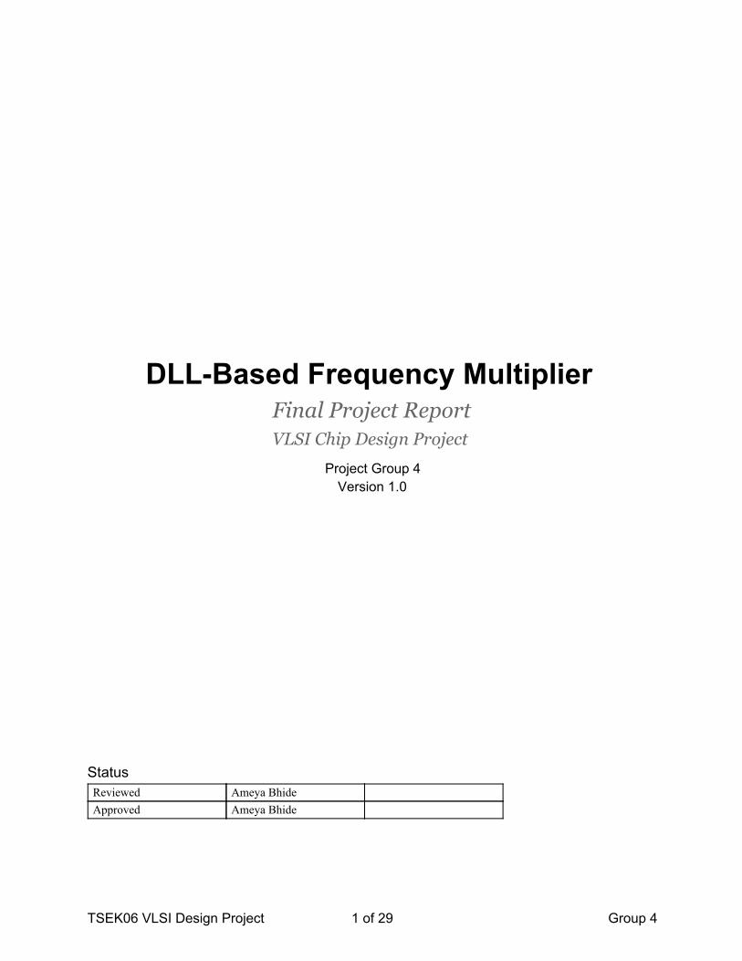
PROJECT IDENTITYProject group 4, 2012/Spring
Linköping University, ISY, Electronic Devices
Name Responsibility Phone EmailHenrik Larsson 073841 30 32 [email protected] Marklund 070684 35 62 [email protected] Moberg Project leader (PL) 070393 84 49 [email protected]
Course responsible: Atila Alvandpour, [email protected] and Supervisor: Ameya Bhide
Office: Bhouse 2B:229:218, 581 00 LINKÖPING, Phone: 013288946, Fax: 013139282Email: [email protected]
TSEK06 VLSI Design Project 2 of 29 Group 4
IntroductionSystem Description
TimingBlock Level and Description
Phase DetectorClock DividerCounterDelay LineTransition DetectorEdge Combiner
Symmetric ANDTPL
Simulation ResultsPAD Assignments / Early Test Plan
PinsRisks and DelaysProject EvaluationReferencesTime Report
TSEK06 VLSI Design Project 3 of 29 Group 4
IntroductionWe are using a pure digital approach to realize a DLLbased frequency multiplier. It uses amultiplier of 8x and is primarily designed for an output frequency of 1GHz, although the actualoutput range is subject to process variations.
The input frequency range designed for at the start was approximately 125250 MHz for an 8xmultiplier and 250500 MHz for a 4x multiplier, enabling an output frequency between 1 GHz and2 GHz. But due to problems with the sizing of the delay line the input range is now around100130 MHz with variations depending on transistor corners. There is also no option for a 4xmultiplier since it was no longer needed.
TSEK06 VLSI Design Project 4 of 29 Group 4
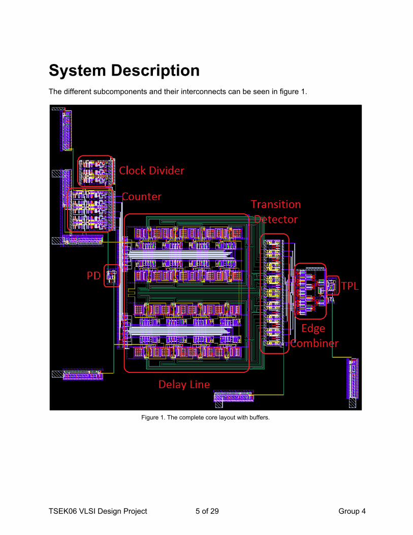
System DescriptionThe different subcomponents and their interconnects can be seen in figure 1.
Figure 1. The complete core layout with buffers.
TSEK06 VLSI Design Project 5 of 29 Group 4
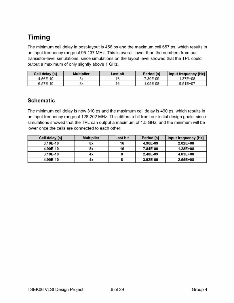
TimingThe minimum cell delay in postlayout is 456 ps and the maximum cell 657 ps, which results inan input frequency range of 95137 MHz. This is overall lower than the numbers from ourtransistorlevel simulations, since simulations on the layout level showed that the TPL couldoutput a maximum of only slightly above 1 GHz.
Cell delay [s] Multiplier Last bit Period [s] Input frequency [Hz]4.56E10 8x 16 7.30E09 1.37E+086.57E10 8x 16 1.05E08 9.51E+07
Schematic
The minimum cell delay is now 310 ps and the maximum cell delay is 490 ps, which results inan input frequency range of 128202 MHz. This differs a bit from our initial design goals, sincesimulations showed that the TPL can output a maximum of 1.5 GHz, and the minimum will belower once the cells are connected to each other.
Cell delay [s] Multiplier Last bit Period [s] Input frequency [Hz]3.10E10 8x 16 4.96E09 2.02E+084.90E10 8x 16 7.84E09 1.28E+083.10E10 4x 8 2.48E09 4.03E+084.90E10 4x 8 3.92E09 2.55E+08
TSEK06 VLSI Design Project 6 of 29 Group 4
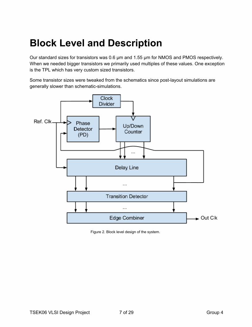
Block Level and DescriptionOur standard sizes for transistors was 0.6 µm and 1.55 µm for NMOS and PMOS respectively.When we needed bigger transistors we primarily used multiples of these values. One exceptionis the TPL which has very custom sized transistors.
Some transistor sizes were tweaked from the schematics since postlayout simulations aregenerally slower than schematicsimulations.
Figure 2. Block level design of the system.
TSEK06 VLSI Design Project 7 of 29 Group 4
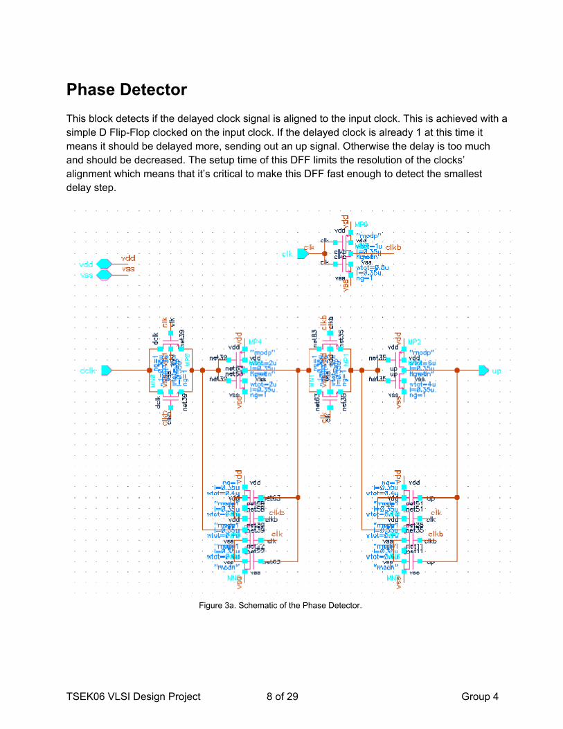
Phase DetectorThis block detects if the delayed clock signal is aligned to the input clock. This is achieved with asimple D FlipFlop clocked on the input clock. If the delayed clock is already 1 at this time itmeans it should be delayed more, sending out an up signal. Otherwise the delay is too muchand should be decreased. The setup time of this DFF limits the resolution of the clocks’alignment which means that it’s critical to make this DFF fast enough to detect the smallestdelay step.
Figure 3a. Schematic of the Phase Detector.
TSEK06 VLSI Design Project 8 of 29 Group 4
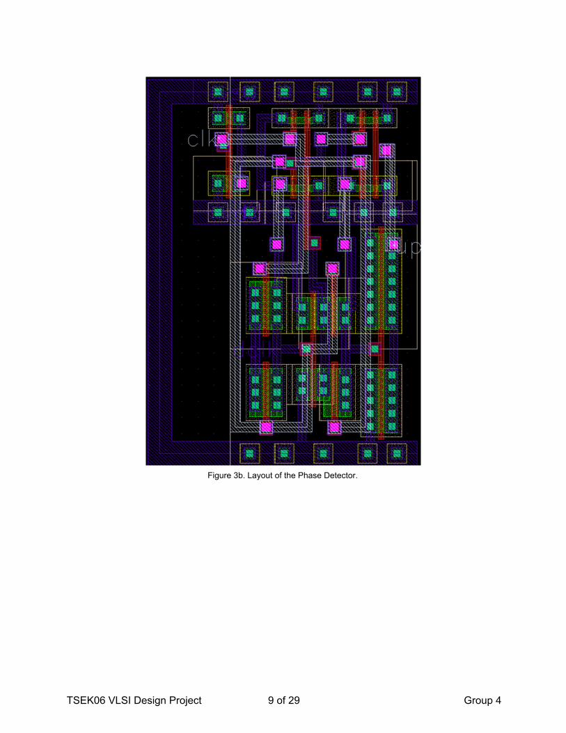
Figure 3b. Layout of the Phase Detector.
TSEK06 VLSI Design Project 9 of 29 Group 4
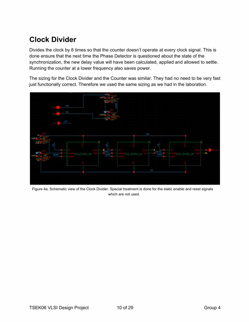
Clock DividerDivides the clock by 8 times so that the counter doesn’t operate at every clock signal. This isdone ensure that the next time the Phase Detector is questioned about the state of thesynchronization, the new delay value will have been calculated, applied and allowed to settle.Running the counter at a lower frequency also saves power.
The sizing for the Clock Divider and the Counter was similar. They had no need to be very fastjust functionally correct. Therefore we used the same sizing as we had in the laboration.
Figure 4a. Schematic view of the Clock Divider. Special treatment is done for the static enable and reset signalswhich are not used.
TSEK06 VLSI Design Project 10 of 29 Group 4
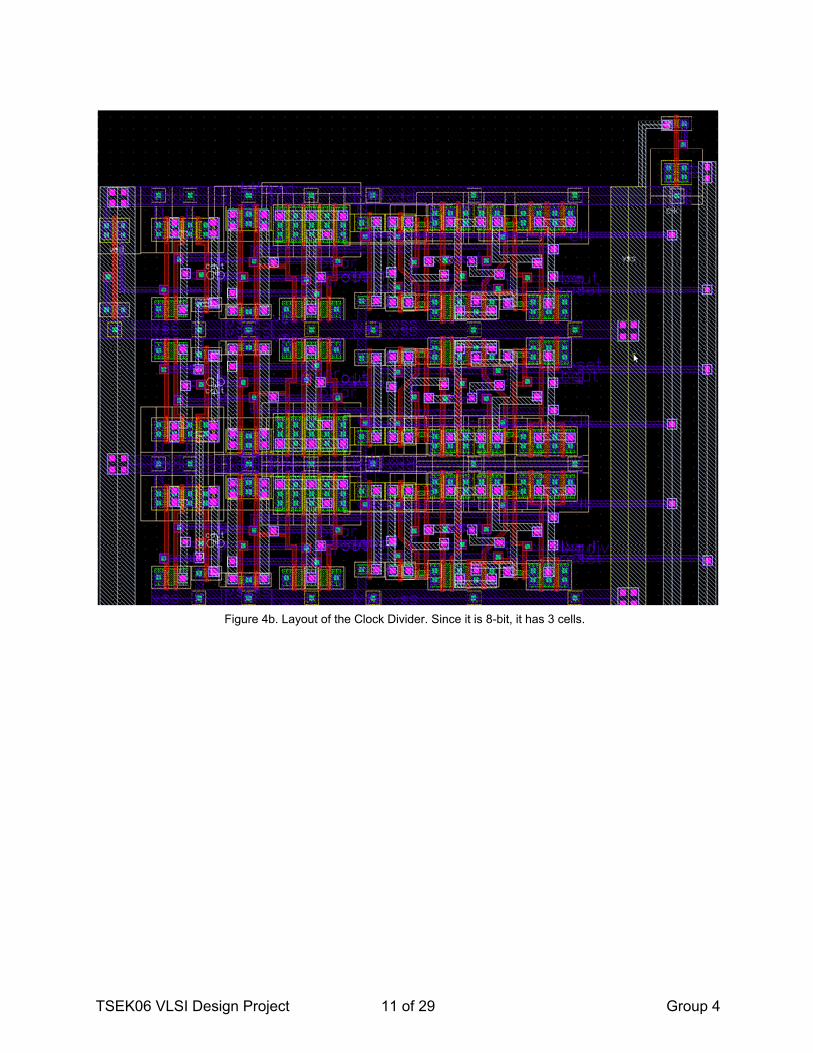
Figure 4b. Layout of the Clock Divider. Since it is 8bit, it has 3 cells.
TSEK06 VLSI Design Project 11 of 29 Group 4
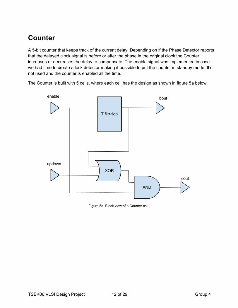
CounterA 5bit counter that keeps track of the current delay. Depending on if the Phase Detector reportsthat the delayed clock signal is before or after the phase in the original clock the Counterincreases or decreases the delay to compensate. The enable signal was implemented in casewe had time to create a lock detector making it possible to put the counter in standby mode. It’snot used and the counter is enabled all the time.
The Counter is built with 5 cells, where each cell has the design as shown in figure 5a below.
Figure 5a. Block view of a Counter cell.
TSEK06 VLSI Design Project 12 of 29 Group 4
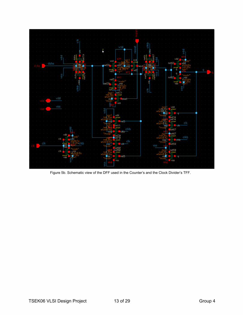
Figure 5b. Schematic view of the DFF used in the Counter’s and the Clock Divider’s TFF.
TSEK06 VLSI Design Project 13 of 29 Group 4
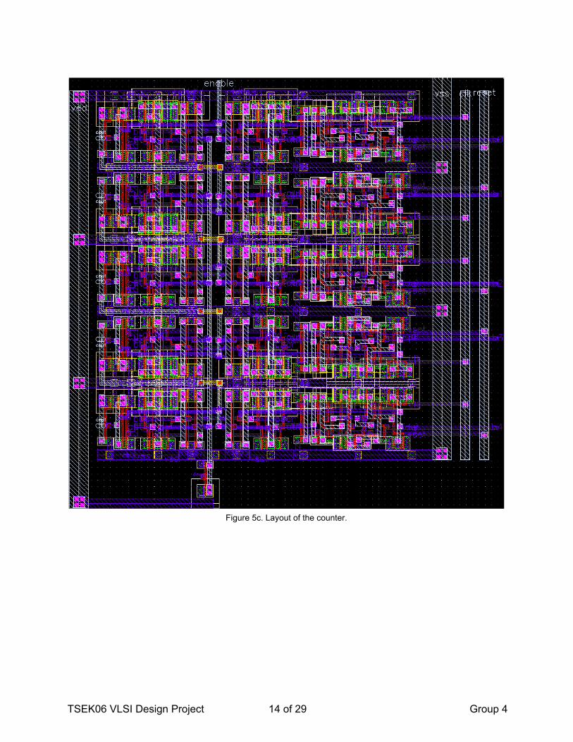
Figure 5c. Layout of the counter.
TSEK06 VLSI Design Project 14 of 29 Group 4
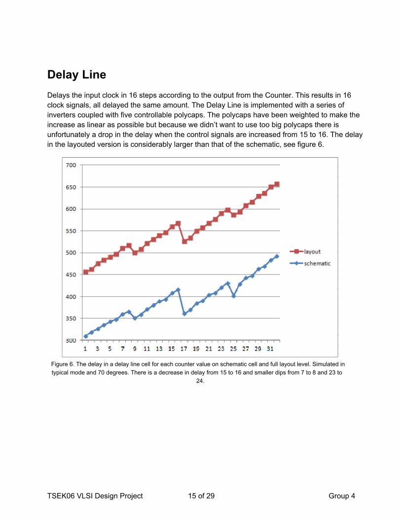
Delay LineDelays the input clock in 16 steps according to the output from the Counter. This results in 16clock signals, all delayed the same amount. The Delay Line is implemented with a series ofinverters coupled with five controllable polycaps. The polycaps have been weighted to make theincrease as linear as possible but because we didn’t want to use too big polycaps there isunfortunately a drop in the delay when the control signals are increased from 15 to 16. The delayin the layouted version is considerably larger than that of the schematic, see figure 6.
Figure 6. The delay in a delay line cell for each counter value on schematic cell and full layout level. Simulated intypical mode and 70 degrees. There is a decrease in delay from 15 to 16 and smaller dips from 7 to 8 and 23 to
24.
TSEK06 VLSI Design Project 15 of 29 Group 4
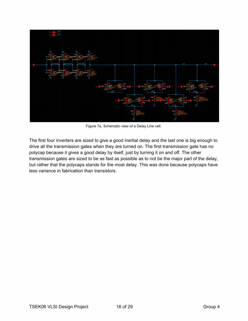
Figure 7a. Schematic view of a Delay Line cell.
The first four inverters are sized to give a good inertial delay and the last one is big enough todrive all the transmission gates when they are turned on. The first transmission gate has nopolycap because it gives a good delay by itself, just by turning it on and off. The othertransmission gates are sized to be as fast as possible as to not be the major part of the delay,but rather that the polycaps stands for the most delay. This was done because polycaps haveless variance in fabrication than transistors.
TSEK06 VLSI Design Project 16 of 29 Group 4
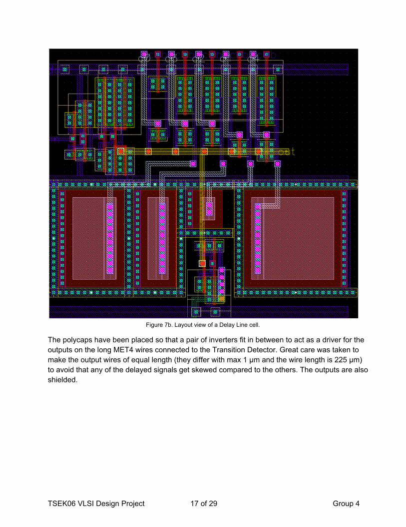
Figure 7b. Layout view of a Delay Line cell.
The polycaps have been placed so that a pair of inverters fit in between to act as a driver for theoutputs on the long MET4 wires connected to the Transition Detector. Great care was taken tomake the output wires of equal length (they differ with max 1 µm and the wire length is 225 µm)to avoid that any of the delayed signals get skewed compared to the others. The outputs are alsoshielded.
TSEK06 VLSI Design Project 17 of 29 Group 4
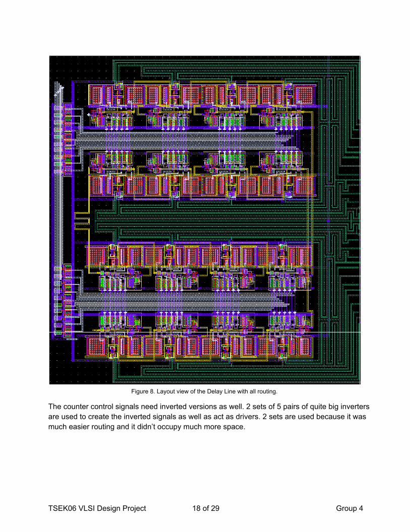
Figure 8. Layout view of the Delay Line with all routing.
The counter control signals need inverted versions as well. 2 sets of 5 pairs of quite big invertersare used to create the inverted signals as well as act as drivers. 2 sets are used because it wasmuch easier routing and it didn’t occupy much more space.
TSEK06 VLSI Design Project 18 of 29 Group 4
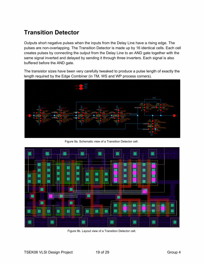
Transition DetectorOutputs short negative pulses when the inputs from the Delay Line have a rising edge. Thepulses are nonoverlapping. The Transition Detector is made up by 16 identical cells. Each cellcreates pulses by connecting the output from the Delay Line to an AND gate together with thesame signal inverted and delayed by sending it through three inverters. Each signal is alsobuffered before the AND gate.
The transistor sizes have been very carefully tweaked to produce a pulse length of exactly thelength required by the Edge Combiner (in TM, WS and WP process corners).
Figure 9a. Schematic view of a Transition Detector cell.
Figure 9b. Layout view of a Transition Detector cell.
TSEK06 VLSI Design Project 19 of 29 Group 4
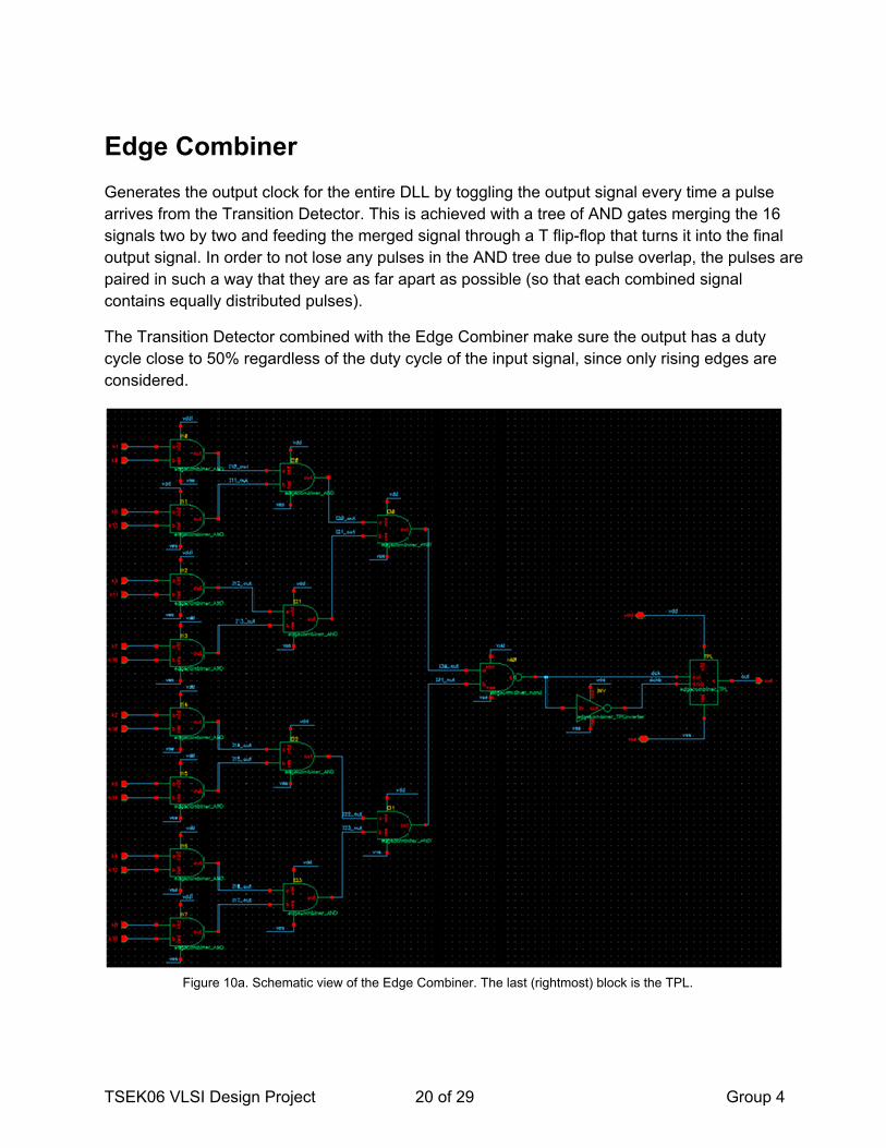
Edge CombinerGenerates the output clock for the entire DLL by toggling the output signal every time a pulsearrives from the Transition Detector. This is achieved with a tree of AND gates merging the 16signals two by two and feeding the merged signal through a T flipflop that turns it into the finaloutput signal. In order to not lose any pulses in the AND tree due to pulse overlap, the pulses arepaired in such a way that they are as far apart as possible (so that each combined signalcontains equally distributed pulses).
The Transition Detector combined with the Edge Combiner make sure the output has a dutycycle close to 50% regardless of the duty cycle of the input signal, since only rising edges areconsidered.
Figure 10a. Schematic view of the Edge Combiner. The last (rightmost) block is the TPL.
TSEK06 VLSI Design Project 20 of 29 Group 4
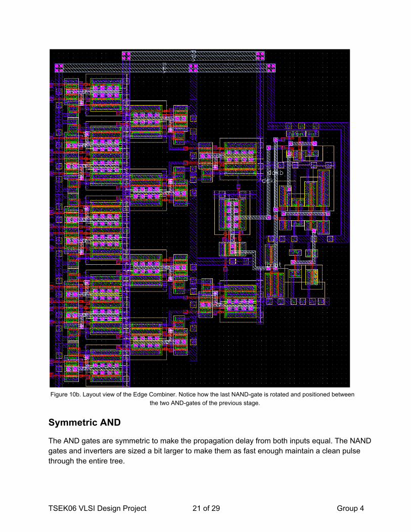
Figure 10b. Layout view of the Edge Combiner. Notice how the last NANDgate is rotated and positioned betweenthe two ANDgates of the previous stage.
Symmetric AND
The AND gates are symmetric to make the propagation delay from both inputs equal. The NANDgates and inverters are sized a bit larger to make them as fast enough maintain a clean pulsethrough the entire tree.
TSEK06 VLSI Design Project 21 of 29 Group 4
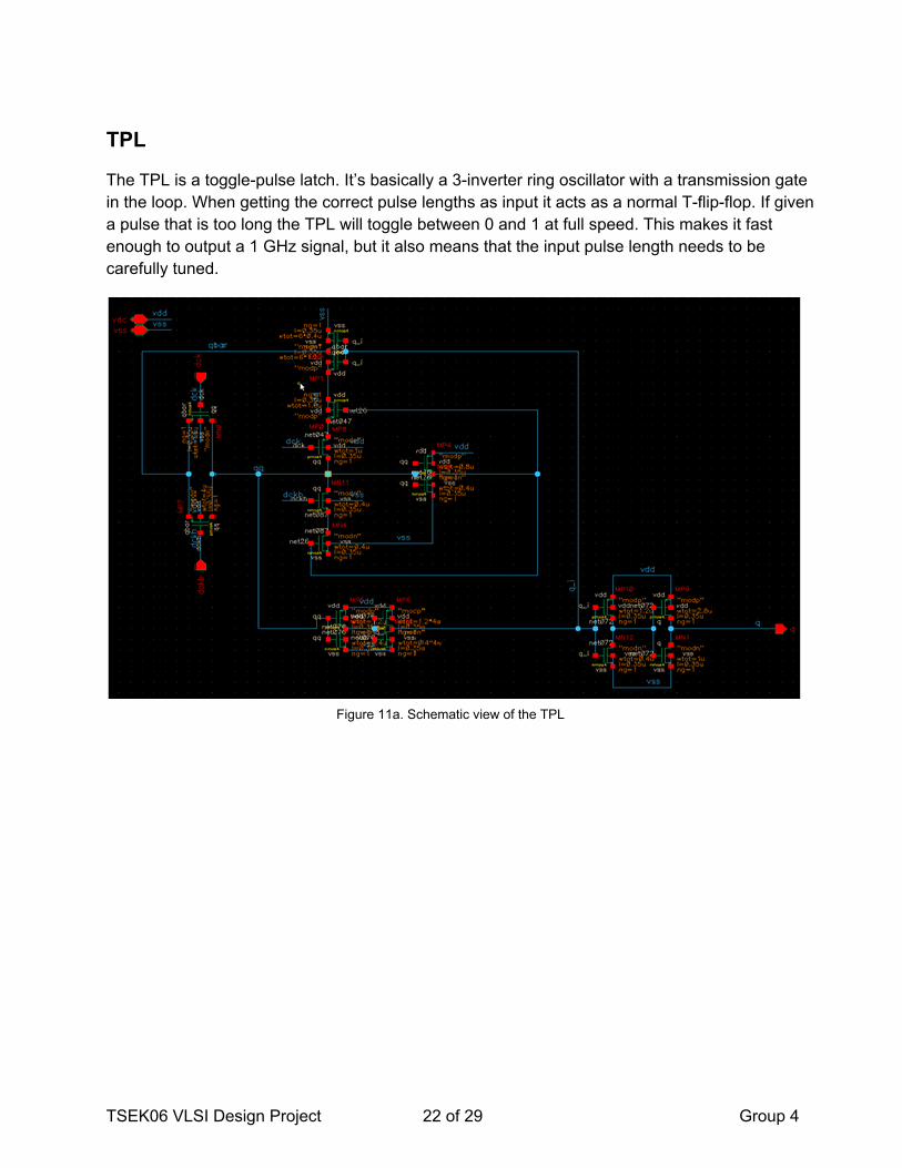
TPL
The TPL is a togglepulse latch. It’s basically a 3inverter ring oscillator with a transmission gatein the loop. When getting the correct pulse lengths as input it acts as a normal Tflipflop. If givena pulse that is too long the TPL will toggle between 0 and 1 at full speed. This makes it fastenough to output a 1 GHz signal, but it also means that the input pulse length needs to becarefully tuned.
Figure 11a. Schematic view of the TPL
TSEK06 VLSI Design Project 22 of 29 Group 4
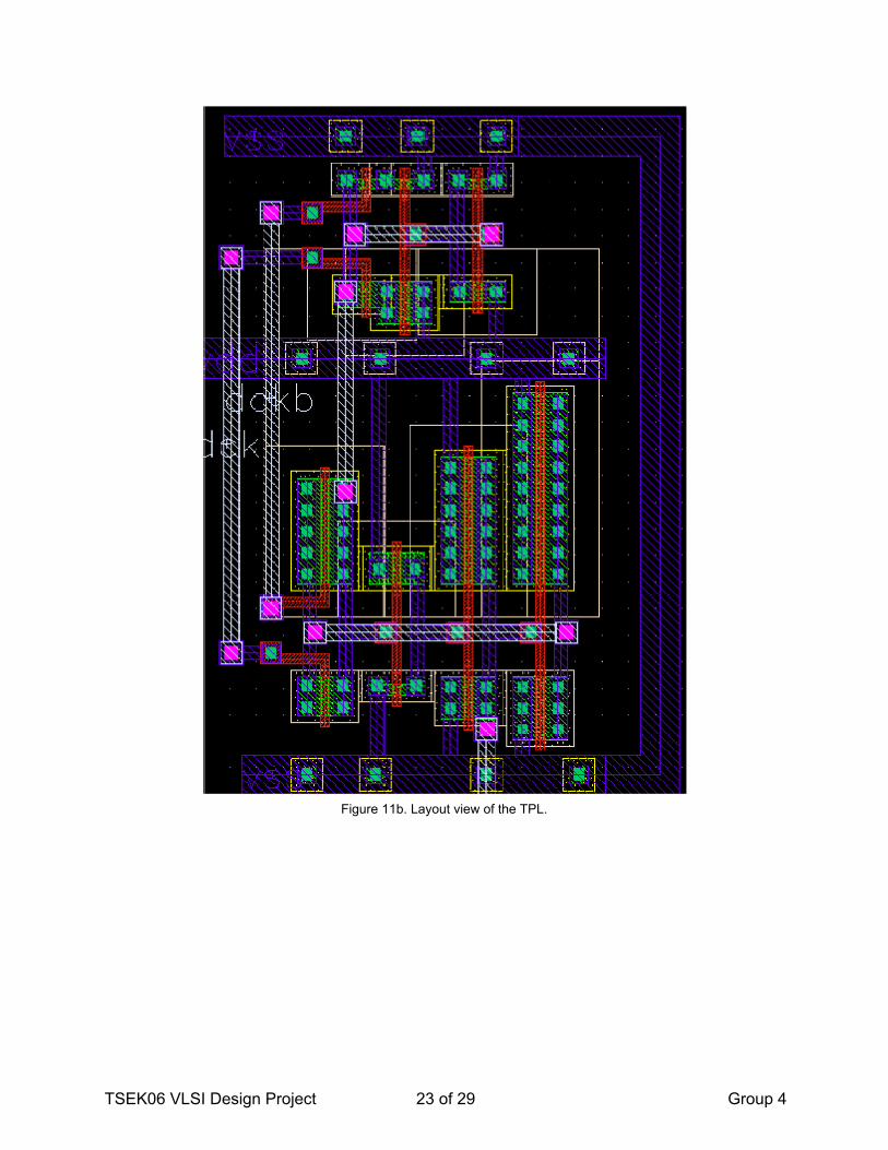
Figure 11b. Layout view of the TPL.
TSEK06 VLSI Design Project 23 of 29 Group 4
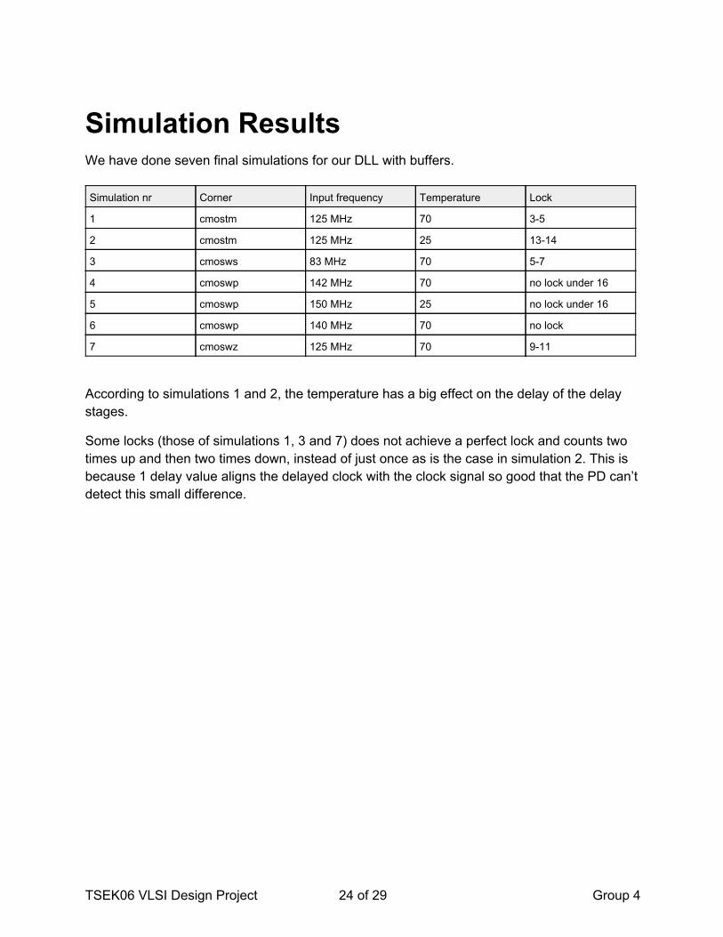
Simulation ResultsWe have done seven final simulations for our DLL with buffers.
Simulation nr Corner Input frequency Temperature Lock
1 cmostm 125 MHz 70 35
2 cmostm 125 MHz 25 1314
3 cmosws 83 MHz 70 57
4 cmoswp 142 MHz 70 no lock under 16
5 cmoswp 150 MHz 25 no lock under 16
6 cmoswp 140 MHz 70 no lock
7 cmoswz 125 MHz 70 911
According to simulations 1 and 2, the temperature has a big effect on the delay of the delaystages.
Some locks (those of simulations 1, 3 and 7) does not achieve a perfect lock and counts twotimes up and then two times down, instead of just once as is the case in simulation 2. This isbecause 1 delay value aligns the delayed clock with the clock signal so good that the PD can’tdetect this small difference.
TSEK06 VLSI Design Project 24 of 29 Group 4
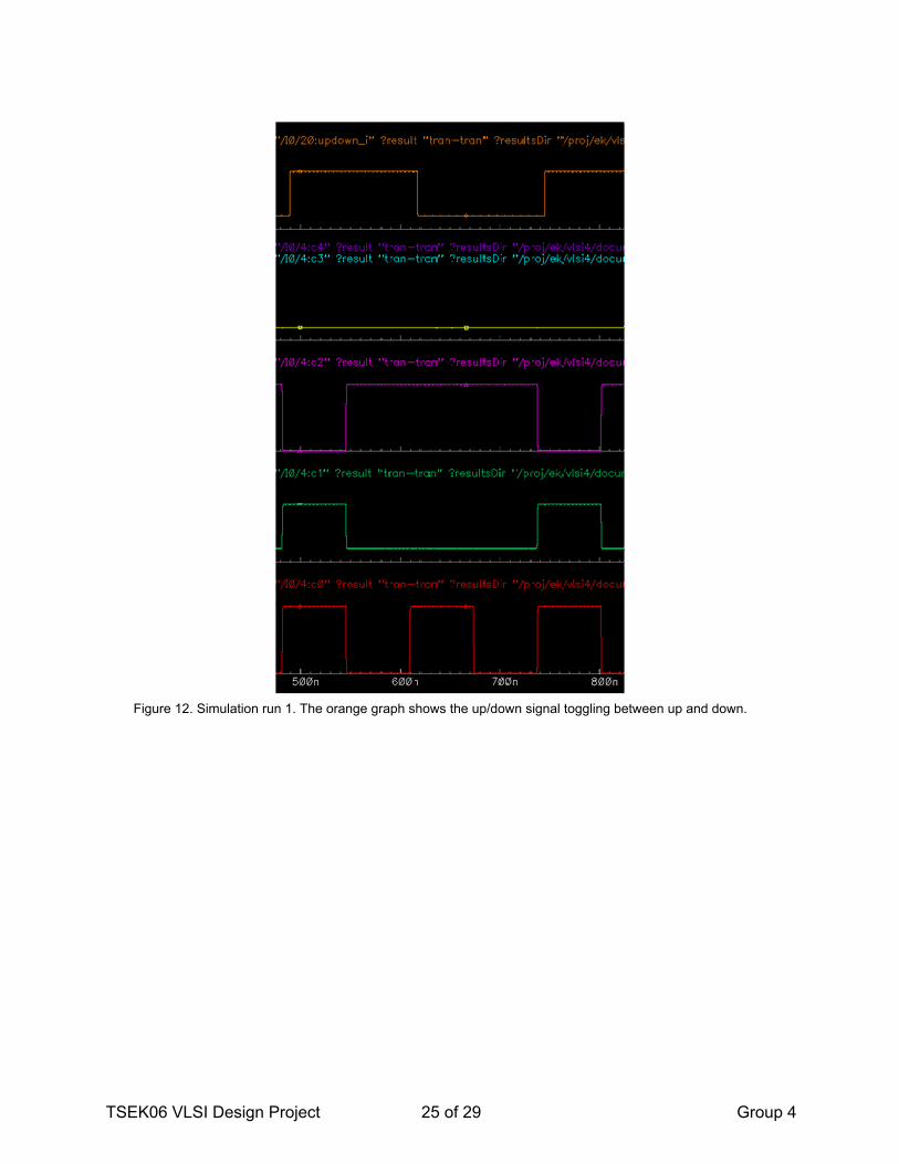
Figure 12. Simulation run 1. The orange graph shows the up/down signal toggling between up and down.
TSEK06 VLSI Design Project 25 of 29 Group 4
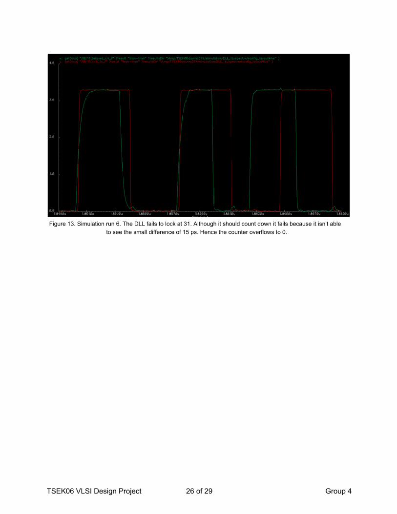
Figure 13. Simulation run 6. The DLL fails to lock at 31. Although it should count down it fails because it isn’t ableto see the small difference of 15 ps. Hence the counter overflows to 0.
TSEK06 VLSI Design Project 26 of 29 Group 4

PAD Assignments / Early Test Plan
PinsWe have 12 pins available, and our pin configuration is as follows:
● 6 input pins○ Vdd○ Vdd for the Delay Line○ Vdd for the Transition Detector○ Vss○ Reset (for the counter)○ Input clock
● 4 output pins○ Delayed clock, the other input to the Phase Detector○ Resulting down/up signal from the Phase Detector○ One of the pulses from the Transition Detector, p15○ Output clock
This configuration uses 10 pins. The output clock is our main output. The other three outputs aretest pins. With the down/up signal we can see if the DLL has achieved a lock (signal switching)or not (signal constantly 0 or 1).
The delayed clock signal shows how the clock has propagated through the Delay Line and thepulse signal will show if the Transition Detector delivers a pulse or not. Because of the shortwidth of the pulse we will probably not be able to measure its width.
TSEK06 VLSI Design Project 27 of 29 Group 4
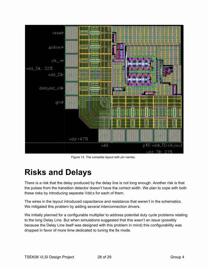
Figure 14. The complete layout with pin names.
Risks and DelaysThere is a risk that the delay produced by the delay line is not long enough. Another risk is thatthe pulses from the transition detector doesn’t have the correct width. We plan to cope with boththese risks by introducing separate Vdd:s for each of them.
The wires in the layout introduced capacitance and resistance that weren’t in the schematics.We mitigated this problem by adding several interconnection drivers.
We initially planned for a configurable multiplier to address potential duty cycle problems relatingto the long Delay Line. But when simulations suggested that this wasn’t an issue (possiblybecause the Delay Line itself was designed with this problem in mind) this configurability wasdropped in favor of more time dedicated to tuning the 8x mode.
TSEK06 VLSI Design Project 28 of 29 Group 4
Project EvaluationVery good supervisor!
Lagom amount of work.
Good laborations suited to make the project easier. Some additional virtuoso commands couldbe introduced, like reshape (R) and edit in place (x). A nice schematic command is M. Show thealternative result browser (graph viewer).
References1. JinHan Kim, YoungHo Kwak, SeokRyung Yoon, MooYoung Kim, SooWon Kim, Chulwoo Kim, A CMOS
DLLBased 120MHz to 1.8GHz Clock Generator for Dynamic Frequency Scaling, ISSCC 2005, KoreaUniversity, Seoul, Korea
TSEK06 VLSI Design Project 29 of 29 Group 4