
Digital VLSI Design Lecture 11: Chip Finishing and Signoff
32
January 14, 2021 Disclaimer: This course was prepared, in its entirety, by Adam Teman. Many materials were copied from sources freely available on the internet. When possible, these sources have been cited; however, some references may have been cited incorrectly or overlooked. If you feel that a picture, graph, or code example has been copied from you and either needs to be cited or removed, please feel free to email adam [email protected] and I will address this as soon as possible. Digital VLSI Design Lecture 11: Chip Finishing and Signoff Lecturer: Dr. Adam Teman
Transcript of Digital VLSI Design Lecture 11: Chip Finishing and Signoff

January 14, 2021
Disclaimer: This course was prepared, in its entirety, by Adam Teman. Many materials were copied from sources freely available on the internet. When possible, these sources have been cited;
however, some references may have been cited incorrectly or overlooked. If you feel that a picture, graph, or code example has been copied from you and either needs to be cited or removed,
please feel free to email [email protected] and I will address this as soon as possible.
Digital VLSI Design
Lecture 11: Chip Finishing and Signoff
Lecturer: Dr. Adam Teman

January 14, 2021© Adam Teman,
Lecture Outline
Sign-off TimingAdvanced Concepts in Static Timing Analysis
3
1
Sign-off Timing
2
Chip Finishing and
Sign-off Checks
January 14, 2021© Adam Teman,
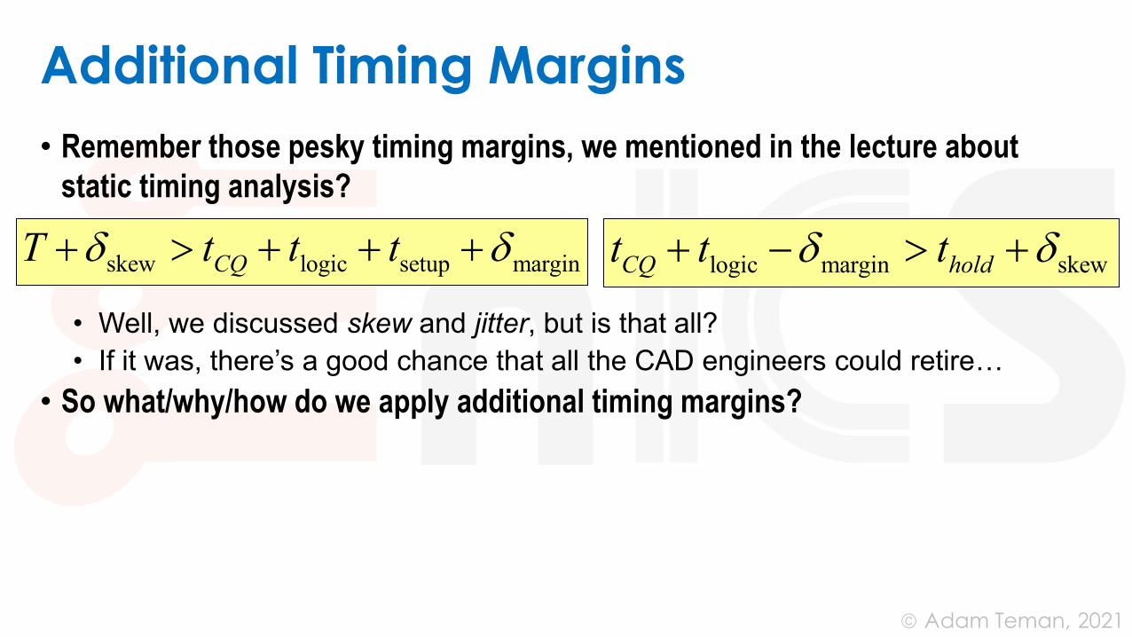
Additional Timing Margins
• Remember those pesky timing margins, we mentioned in the lecture about
static timing analysis?
• Well, we discussed skew and jitter, but is that all?
• If it was, there’s a good chance that all the CAD engineers could retire…
• So what/why/how do we apply additional timing margins?
skew logic setup marginCQT t t t + + + +logic margin skewCQ holdt t t + − +

January 14, 2021© Adam Teman,
Best Case-Worst Case (BC-WC) Timing
• This is the straightforward and traditional way to run STA:
• Max-delay (setup) checks are run on worst-case (slow) conditions.
• Min-delay (hold) checks are run on best-case (fast) conditions.
• However, it doesn’t take into account variation that can occur across the chip,
for example, due to a temperature variance.
set_db timing_analysis_type best_case_worst_case
January 14, 2021© Adam Teman,
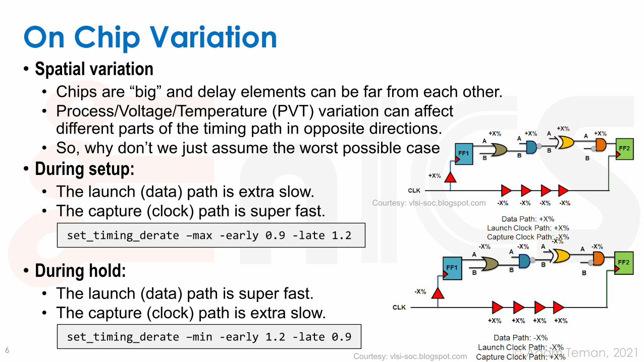
On Chip Variation• Spatial variation
• Chips are “big” and delay elements can be far from each other.
• Process/Voltage/Temperature (PVT) variation can affect different parts of the timing path in opposite directions.
• So, why don’t we just assume the worst possible case
• During setup:• The launch (data) path is extra slow.
• The capture (clock) path is super fast.
• During hold:• The launch (data) path is super fast.
• The capture (clock) path is extra slow.
6
set_timing_derate –max -early 0.9 -late 1.2
set_timing_derate –min -early 1.2 -late 0.9
Courtesy: vlsi-soc.blogspot.com
Courtesy: vlsi-soc.blogspot.com
January 14, 2021© Adam Teman,
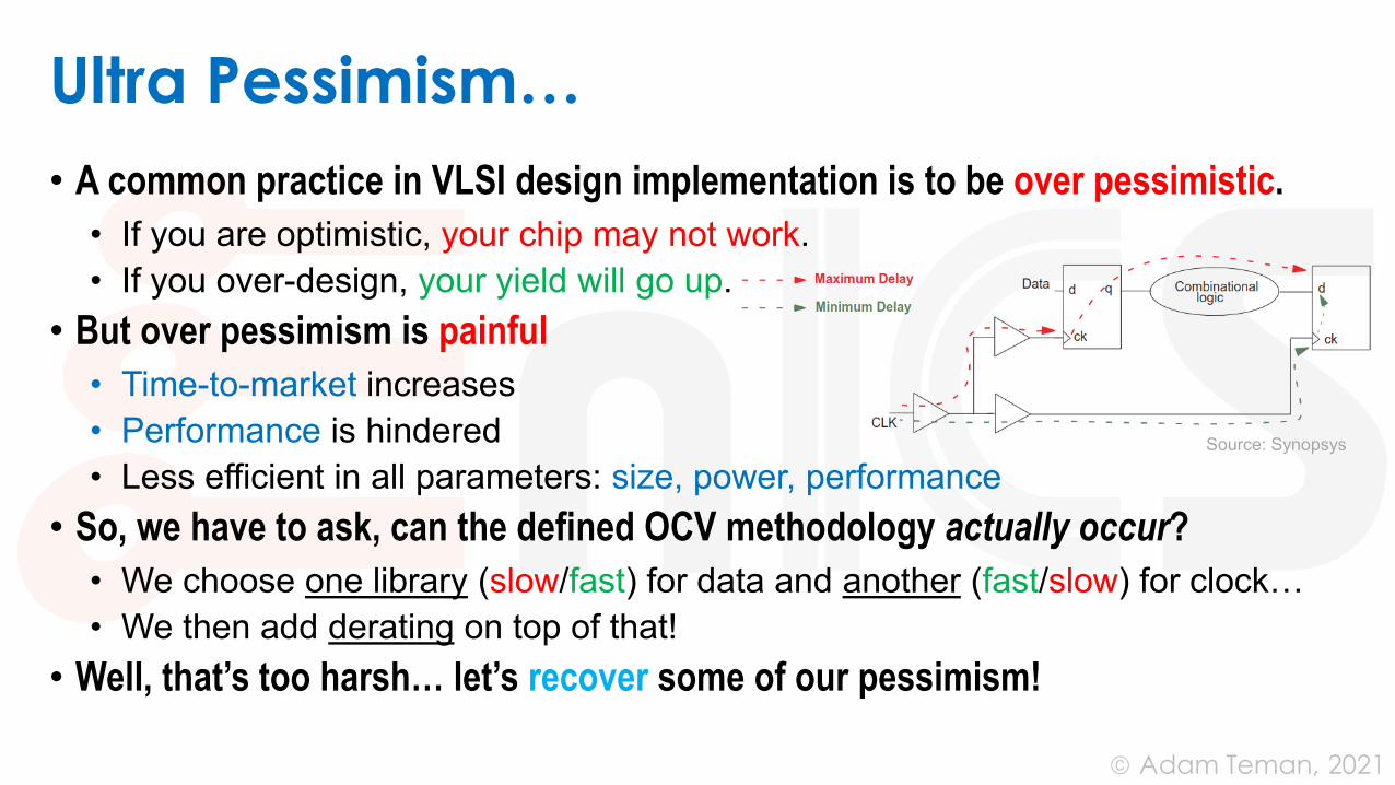
Ultra Pessimism…
• A common practice in VLSI design implementation is to be over pessimistic.
• If you are optimistic, your chip may not work.
• If you over-design, your yield will go up.
• But over pessimism is painful
• Time-to-market increases
• Performance is hindered
• Less efficient in all parameters: size, power, performance
• So, we have to ask, can the defined OCV methodology actually occur?
• We choose one library (slow/fast) for data and another (fast/slow) for clock…
• We then add derating on top of that!
• Well, that’s too harsh… let’s recover some of our pessimism!
Source: Synopsys
January 14, 2021© Adam Teman,
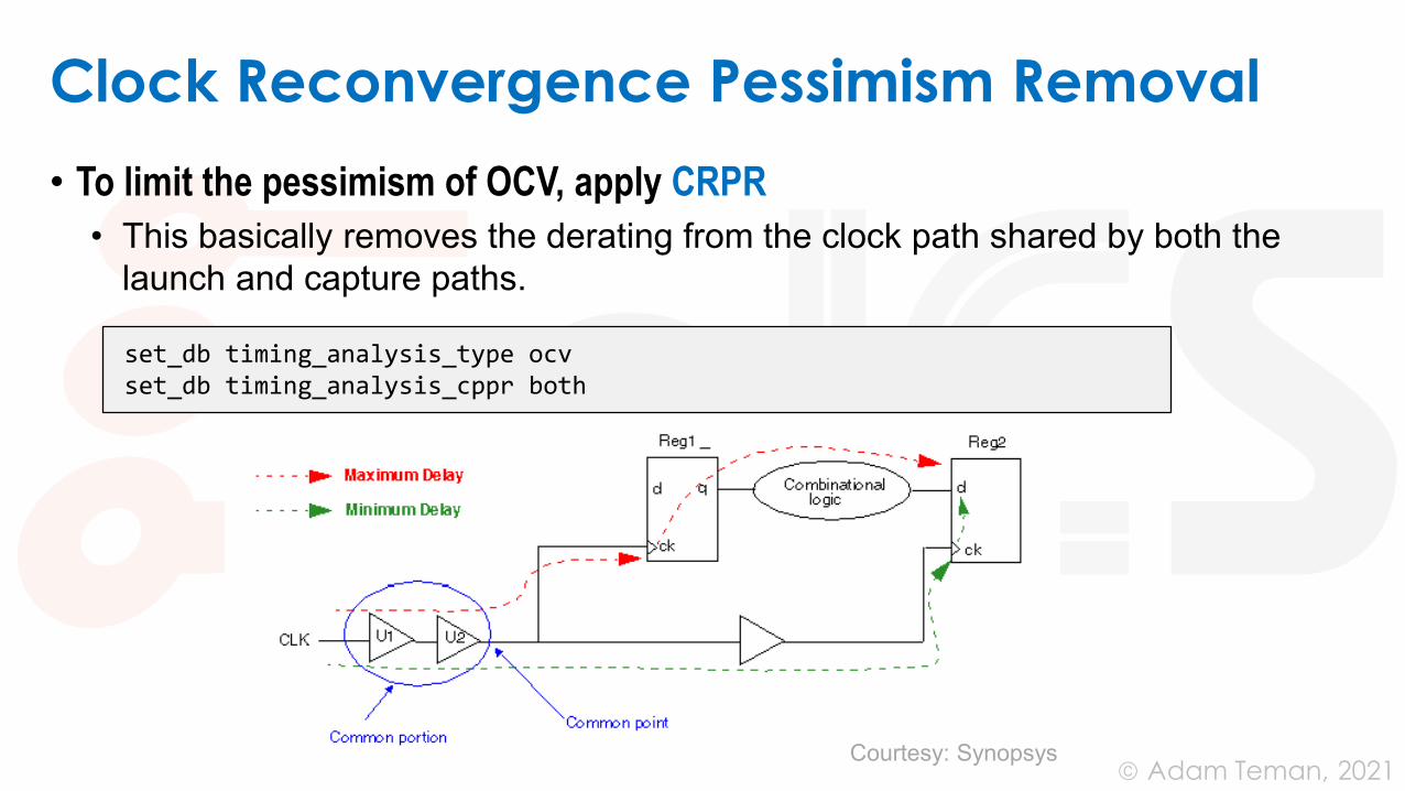
Clock Reconvergence Pessimism Removal
• To limit the pessimism of OCV, apply CRPR
• This basically removes the derating from the clock path shared by both the
launch and capture paths.
Courtesy: Synopsys
set_db timing_analysis_type ocvset_db timing_analysis_cppr both

January 14, 2021© Adam Teman,
Advanced on-chip variation (AOCV)
• Well, CPPR helped, but those derates are gruesome.
• Do all paths derate the same?
• No, variation is statistical…
• But statistical behavior is hard to compute.
• So, let’s do something easier.
• Someone noticed that worst-case conditions in a path depend on:
• Distance between gates on the path
• Depth (number of stages) of the path
• So let’s provide libraries with new derating factors based on these factors.
• We’ll call it “Advanced On-Chip Variation”!
Courtesy: Cadence
update_library_set –name slow –aocv test.aocv.libset_db timing_analysis_aocv true
January 14, 2021© Adam Teman,
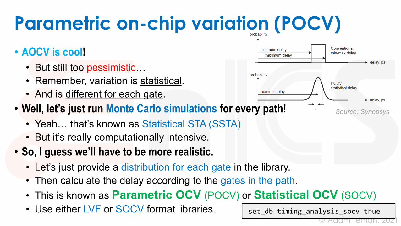
Parametric on-chip variation (POCV)
• AOCV is cool!
• But still too pessimistic…
• Remember, variation is statistical.
• And is different for each gate.
• Well, let’s just run Monte Carlo simulations for every path!
• Yeah… that’s known as Statistical STA (SSTA)
• But it’s really computationally intensive.
• So, I guess we’ll have to be more realistic.
• Let’s just provide a distribution for each gate in the library.
• Then calculate the delay according to the gates in the path.
• This is known as Parametric OCV (POCV) or Statistical OCV (SOCV)
• Use either LVF or SOCV format libraries. set_db timing_analysis_socv true
Source: Synopsys

January 14, 2021© Adam Teman,
Path-based Analysis
• Another point of pessimism removal is to run Path-based Analysis (PBA)
• Due to long runtimes, STA is usually run with Graph-based Analysis (GBA)
• What is the difference?
• GBA chooses the worst case propagation from all
inputs through a gate
• PBA chooses the propagation of the specific path
• This results in a 10X longer run time
but highly reduced pessimism
source:
vlsi-expert.com
January 14, 2021© Adam Teman,
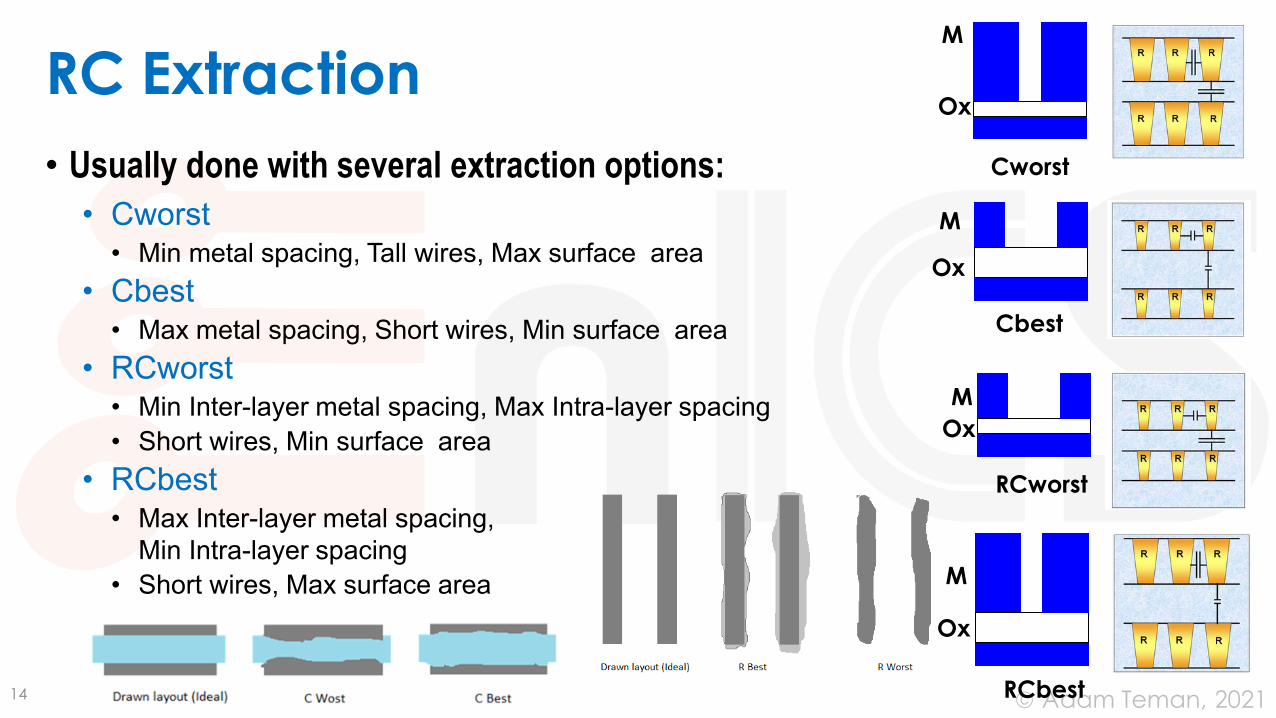
RC Extraction
• Usually done with several extraction options:
• Cworst• Min metal spacing, Tall wires, Max surface area
• Cbest• Max metal spacing, Short wires, Min surface area
• RCworst• Min Inter-layer metal spacing, Max Intra-layer spacing
• Short wires, Min surface area
• RCbest• Max Inter-layer metal spacing,
Min Intra-layer spacing
• Short wires, Max surface area
14
Ox
M
RCbest
Ox
M
RCworst
M
Ox
Cbest
M
Ox
Cworst
January 14, 2021© Adam Teman,
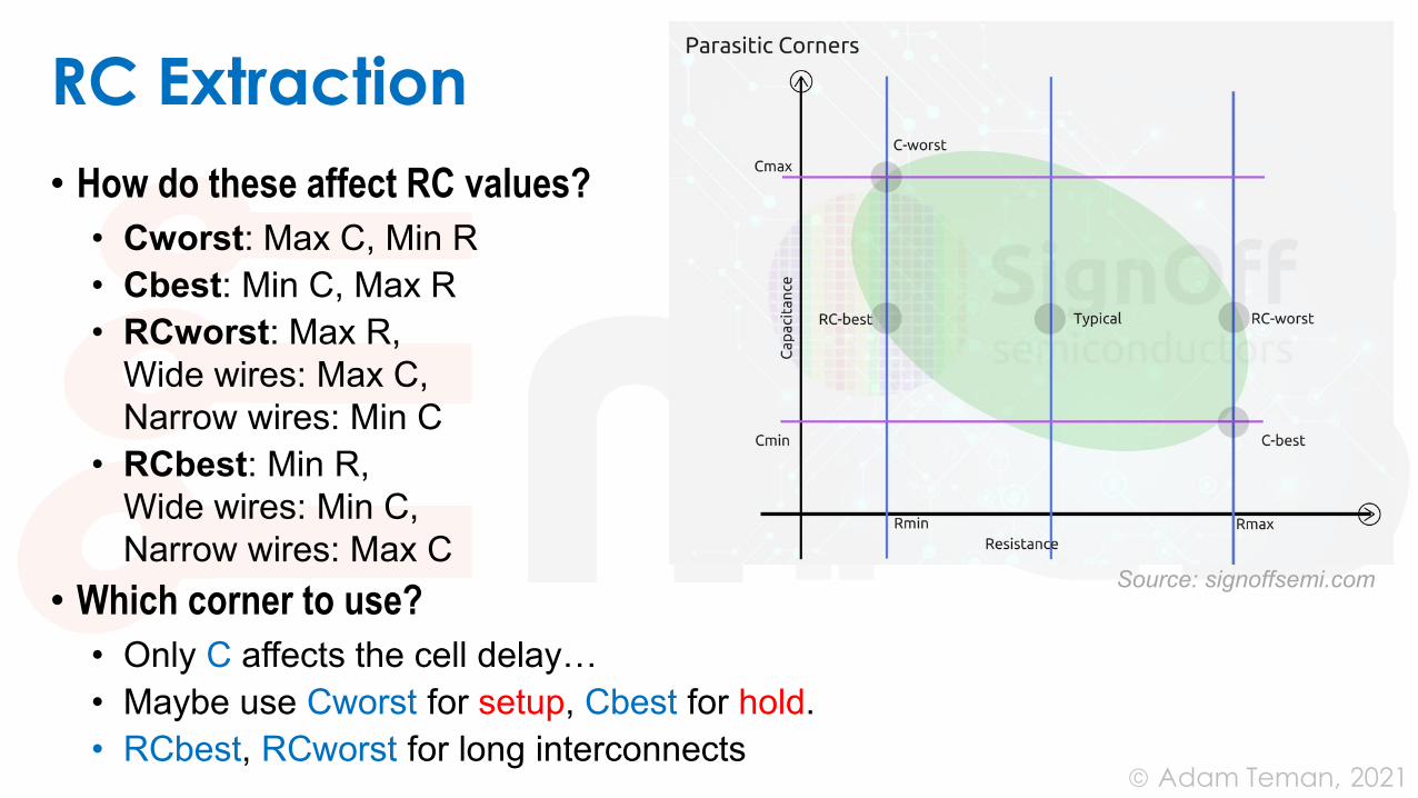
RC Extraction
• How do these affect RC values?
• Cworst: Max C, Min R
• Cbest: Min C, Max R
• RCworst: Max R,
Wide wires: Max C,
Narrow wires: Min C
• RCbest: Min R,
Wide wires: Min C,
Narrow wires: Max C
• Which corner to use?
• Only C affects the cell delay…
• Maybe use Cworst for setup, Cbest for hold.
• RCbest, RCworst for long interconnects
Source: signoffsemi.com
January 14, 2021© Adam Teman,
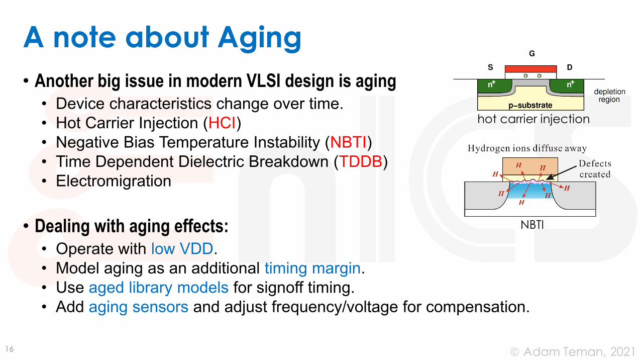
A note about Aging
• Another big issue in modern VLSI design is aging• Device characteristics change over time.
• Hot Carrier Injection (HCI)
• Negative Bias Temperature Instability (NBTI)
• Time Dependent Dielectric Breakdown (TDDB)
• Electromigration
• Dealing with aging effects:• Operate with low VDD.
• Model aging as an additional timing margin.
• Use aged library models for signoff timing.
• Add aging sensors and adjust frequency/voltage for compensation.
16
hot carrier injection
NBTI
January 14, 2021© Adam Teman,
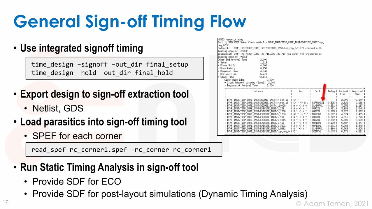
General Sign-off Timing Flow
• Use integrated signoff timing
• Export design to sign-off extraction tool
• Netlist, GDS
• Load parasitics into sign-off timing tool
• SPEF for each corner
• Run Static Timing Analysis in sign-off tool
• Provide SDF for ECO
• Provide SDF for post-layout simulations (Dynamic Timing Analysis)17
time_design –signoff –out_dir final_setuptime_design –hold –out_dir final_hold
read_spef rc_corner1.spef –rc_corner rc_corner1
Chip Finishing and Sign-off
1
Sign-off Timing
2
Chip Finishing and
Sign-off Checks
January 14, 2021© Adam Teman,
Chip Finishing Overview
• Chip Finishing for Signoff includes, at the very least:
• Insertion of fillers and DeCaps.
• Application of Design for Manufacturing (DFM)
and Design for Yield (DFY) rules.
• Antenna checking.
• Metal filling and slotting for metal density rules.
• IR Drop and Electromigration Analysis
• Logic Equivalence
• Layout (Physical) Verification
• Add Sealring
19
January 14, 2021© Adam Teman,
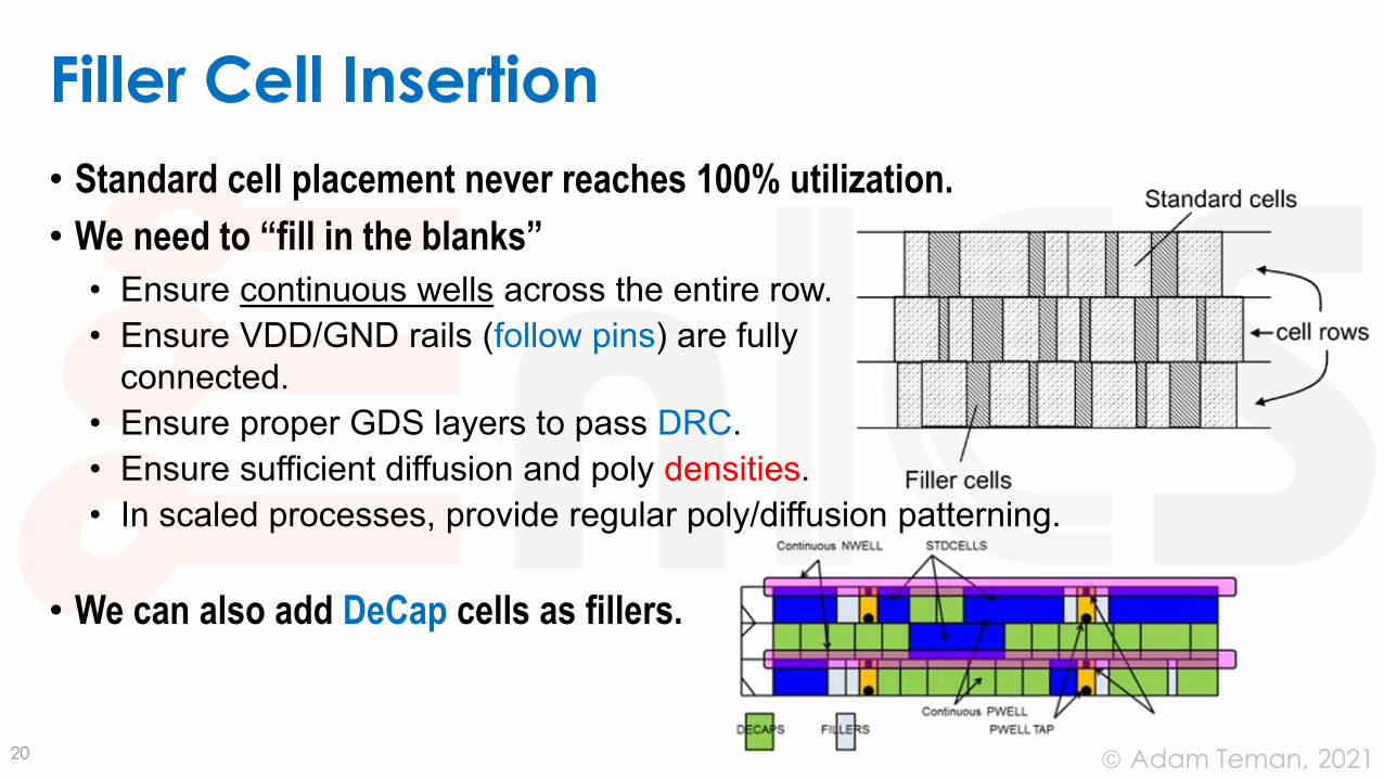
Filler Cell Insertion
• Standard cell placement never reaches 100% utilization.
• We need to “fill in the blanks”
• Ensure continuous wells across the entire row.
• Ensure VDD/GND rails (follow pins) are fully
connected.
• Ensure proper GDS layers to pass DRC.
• Ensure sufficient diffusion and poly densities.
• In scaled processes, provide regular poly/diffusion patterning.
• We can also add DeCap cells as fillers.
20
January 14, 2021© Adam Teman,
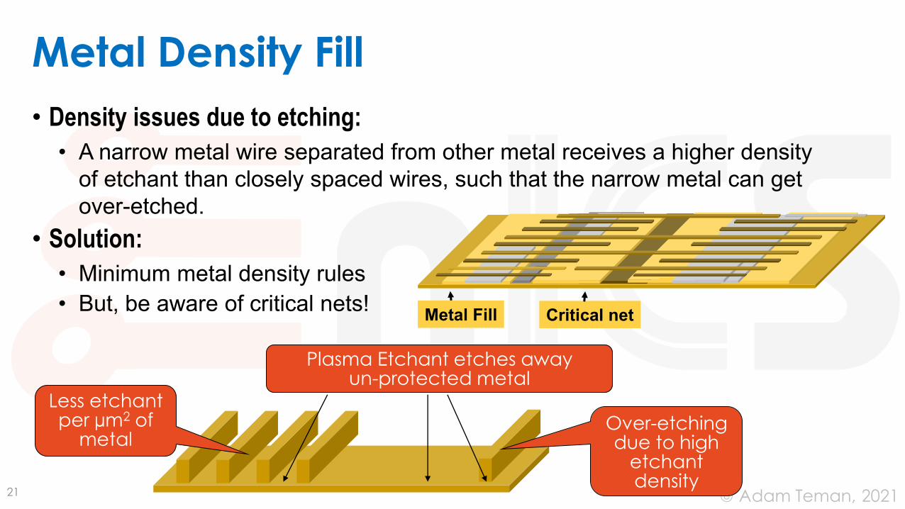
Metal Density Fill
• Density issues due to etching:
• A narrow metal wire separated from other metal receives a higher density
of etchant than closely spaced wires, such that the narrow metal can get
over-etched.
• Solution:
• Minimum metal density rules
• But, be aware of critical nets!
21
Over-etching due to high
etchant density
Less etchant per µm2 of
metal
Plasma Etchant etches awayun-protected metal
Critical netMetal Fill
January 14, 2021© Adam Teman,
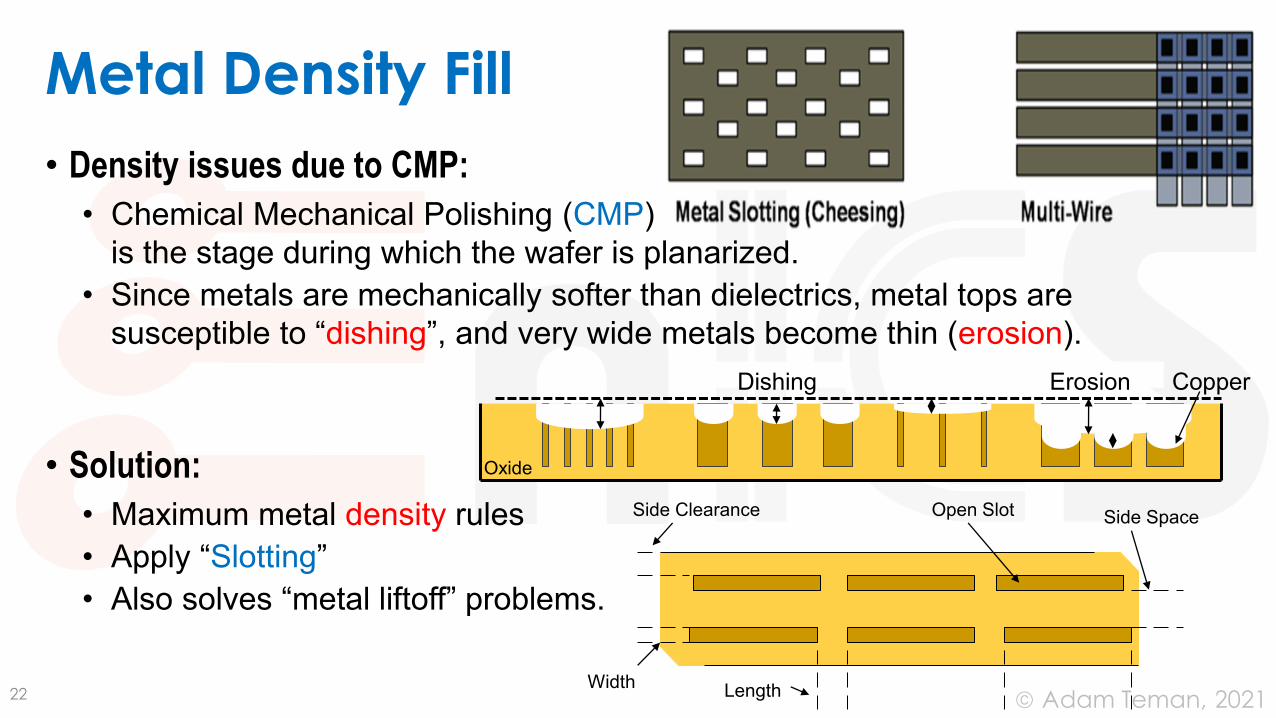
Metal Density Fill
• Density issues due to CMP:
• Chemical Mechanical Polishing (CMP)
is the stage during which the wafer is planarized.
• Since metals are mechanically softer than dielectrics, metal tops are
susceptible to “dishing”, and very wide metals become thin (erosion).
• Solution:
• Maximum metal density rules
• Apply “Slotting”
• Also solves “metal liftoff” problems.
22
CopperErosionDishing
Oxide
Side Clearance Open Slot Side Space
WidthLength
January 14, 2021© Adam Teman,
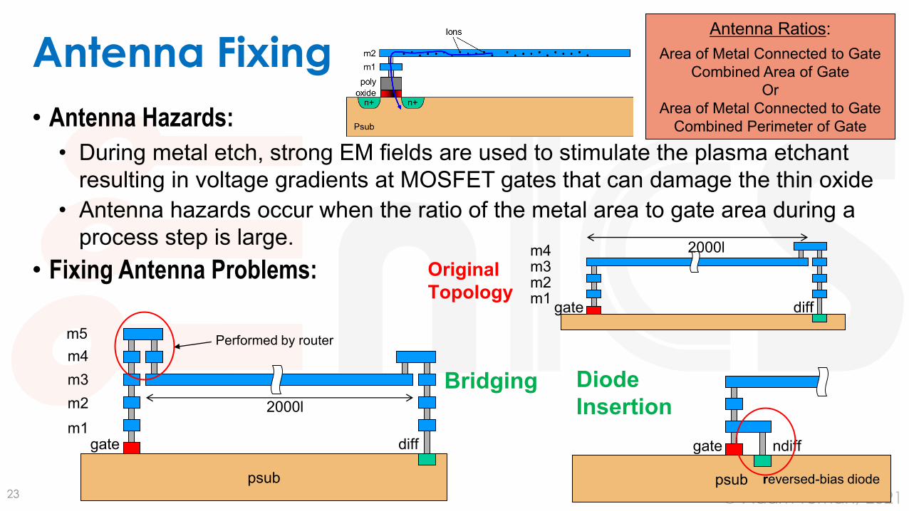
Antenna Fixing
• Antenna Hazards:
• During metal etch, strong EM fields are used to stimulate the plasma etchant
resulting in voltage gradients at MOSFET gates that can damage the thin oxide
• Antenna hazards occur when the ratio of the metal area to gate area during a
process step is large.
• Fixing Antenna Problems:
23
Antenna Ratios:
Area of Metal Connected to Gate
Combined Area of Gate
Or
Area of Metal Connected to Gate
Combined Perimeter of Gate
m4m3m2m1
gate
2000l
diff
Original
Topology
diff
psub
gate
2000l
m4
m3
m2
m1
m5 Performed by router
Bridging
psub
gate ndiff
reversed-bias diode
Diode
Insertion

January 14, 2021© Adam Teman,
IR Drop and EM Analysis
• Static IR drop analysis:
• Average voltage drop assuming constant current.
• Insufficient for modern technologies.
• Dynamic IR drop analysis:
• Depends on switching activity of the logic.
• Is vector dependent, using VCD files
produced with SDF timing data.
• Analyzes peak current demand.
• Often run at FF corner, high VDD, high temp, RCWorst extraction.
• Electromigration Analysis
• Check current density.
• Focuses on power lines, but “Signal EM” is also required nowadays.
25
January 14, 2021© Adam Teman,
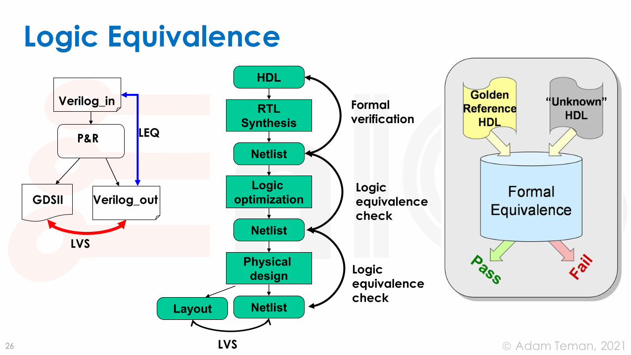
Logic Equivalence
26
Logic
optimization
Physical
design
RTL
Synthesis
HDL
Netlist
Netlist
Netlist
Formal
verification
Logic
equivalence
check
LVS
Layout
Logic
equivalence
check
Verilog_in
P&R
GDSII Verilog_out
LEQ
LVS
January 14, 2021© Adam Teman,
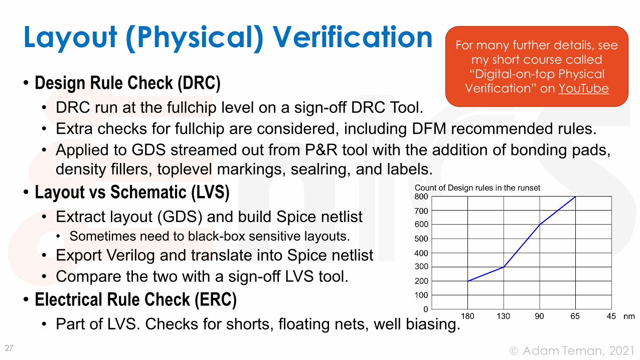
Layout (Physical) Verification
• Design Rule Check (DRC)
• DRC run at the fullchip level on a sign-off DRC Tool.
• Extra checks for fullchip are considered, including DFM recommended rules.
• Applied to GDS streamed out from P&R tool with the addition of bonding pads,
density fillers, toplevel markings, sealring, and labels.
• Layout vs Schematic (LVS)
• Extract layout (GDS) and build Spice netlist• Sometimes need to black-box sensitive layouts.
• Export Verilog and translate into Spice netlist
• Compare the two with a sign-off LVS tool.
• Electrical Rule Check (ERC)
• Part of LVS. Checks for shorts, floating nets, well biasing.
27
For many further details, see
my short course called
“Digital-on-top Physical
Verification” on YouTube
January 14, 2021© Adam Teman,
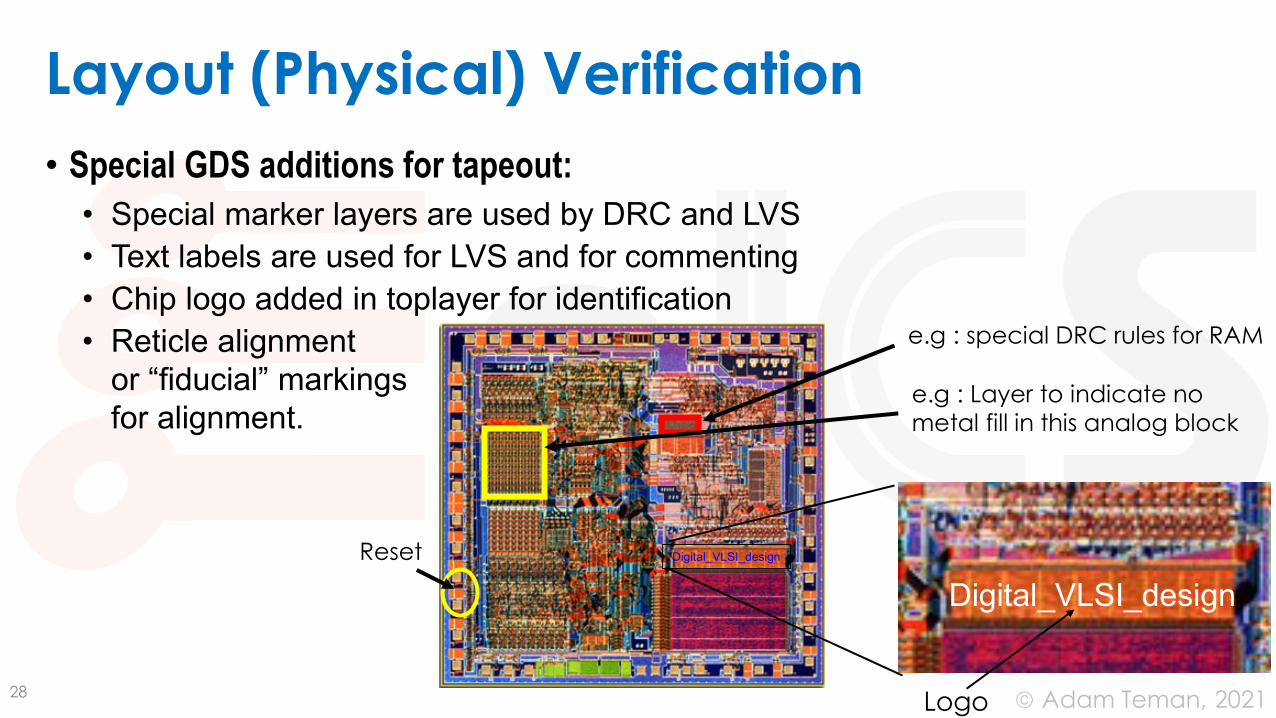
Layout (Physical) Verification
• Special GDS additions for tapeout:
• Special marker layers are used by DRC and LVS
• Text labels are used for LVS and for commenting
• Chip logo added in toplayer for identification
• Reticle alignment
or “fiducial” markings
for alignment.
28
e.g : special DRC rules for RAM
e.g : Layer to indicate no
metal fill in this analog block
Reset
Digital_VLSI_design
Logo
Digital_VLSI_design
January 14, 2021© Adam Teman,
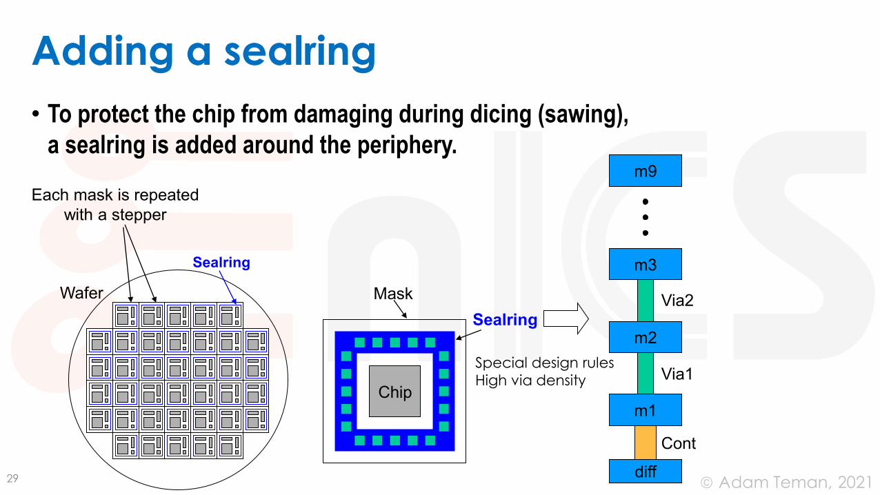
Adding a sealring
• To protect the chip from damaging during dicing (sawing),
a sealring is added around the periphery.
29
Sealring
Each mask is repeated
with a stepper
Wafer
Chip
Sealring
diff
m1
m2
m3
m9
Cont
Via1
Via2Mask
Special design rules
High via density

January 14, 2021© Adam Teman,
Resolution Enhancement Techniques (RET)
• Before writing the mask, additional transformations are applied to
the GDS:
30
90nm and Below130nm180nm
OPC
Design
Mask
Wafer
OPC
0°
180°
0°
180°
PSM
diffraction
feature sizes
➔ light wavelength
January 14, 2021© Adam Teman,
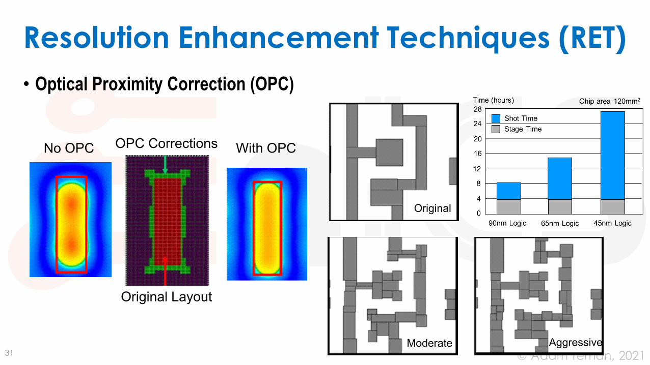
Resolution Enhancement Techniques (RET)
• Optical Proximity Correction (OPC)
31
OPC Corrections
Original Layout
With OPCNo OPC
Original
AggressiveModerate
January 14, 2021© Adam Teman,
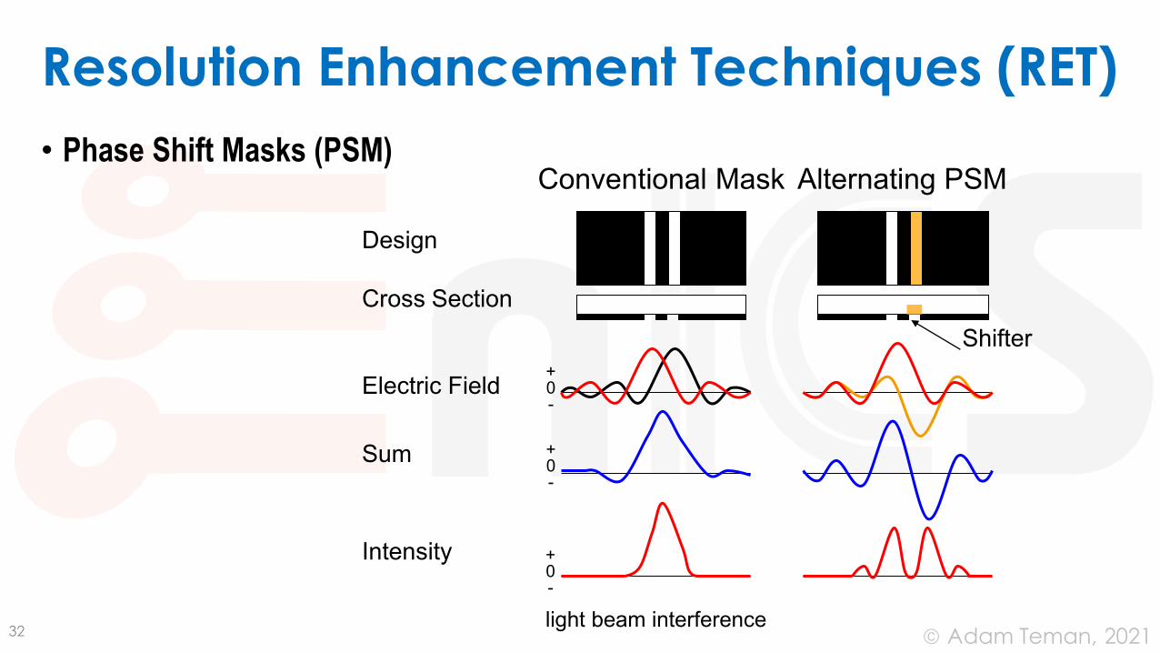
Resolution Enhancement Techniques (RET)
• Phase Shift Masks (PSM)
32
Design
Cross Section
Electric Field
Sum
Intensity
Conventional Mask Alternating PSM
Shifter
+0-
+0-
+0-
light beam interference
January 14, 2021© Adam Teman,
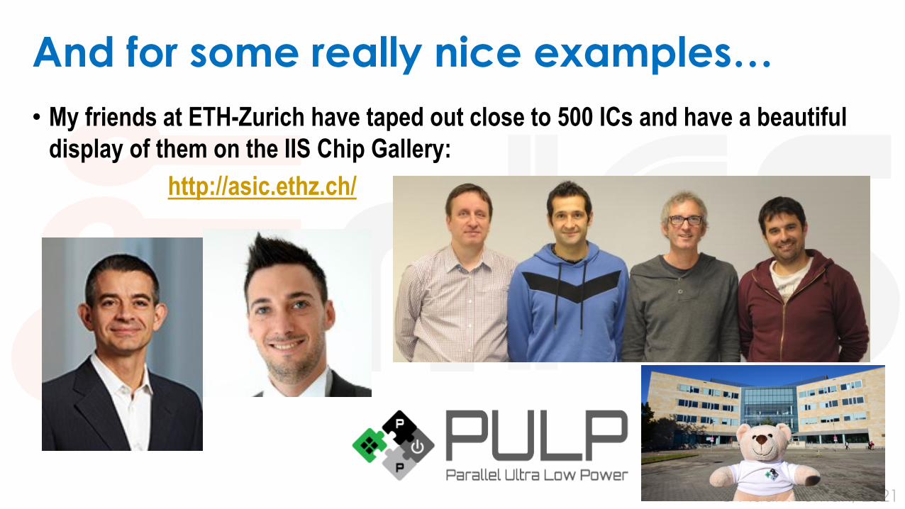
And for some really nice examples…
• My friends at ETH-Zurich have taped out close to 500 ICs and have a beautiful
display of them on the IIS Chip Gallery:
http://asic.ethz.ch/
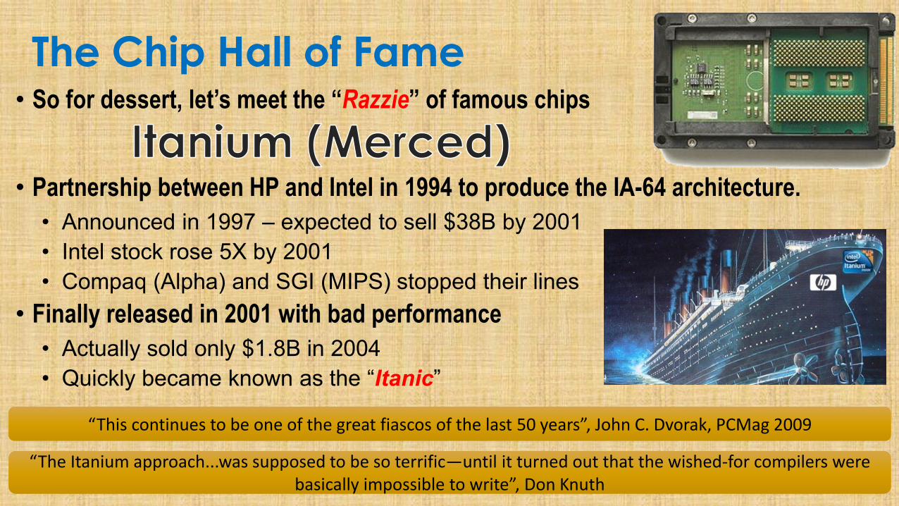
The Chip Hall of Fame• So for dessert, let’s meet the “Razzie” of famous chips
• Partnership between HP and Intel in 1994 to produce the IA-64 architecture.
• Announced in 1997 – expected to sell $38B by 2001
• Intel stock rose 5X by 2001
• Compaq (Alpha) and SGI (MIPS) stopped their lines
• Finally released in 2001 with bad performance
• Actually sold only $1.8B in 2004
• Quickly became known as the “Itanic”
“This continues to be one of the great fiascos of the last 50 years”, John C. Dvorak, PCMag 2009“This continues to be one of the great fiascos of the last 50 years”, John C. Dvorak, PCMag 2009
“The Itanium approach...was supposed to be so terrific—until it turned out that the wished-for compilers were basically impossible to write”, Don Knuth
“The Itanium approach...was supposed to be so terrific—until it turned out that the wished-for compilers were basically impossible to write”, Don Knuth

January 14, 2021© Adam Teman,
Main References
• Rob Rutenbar “From Logic to Layout” 2013
• Synopsys University Courseware
• IDESA
• Kahng, et al. “VLSI Physical Design: From Graph Partitioning to Timing
Closure” – Chapter 6
35


