
E IMPLEMENTATION OF 16-BIT MULTIPLIER …aircconline.com/vlsics/V3N3/3312vlsics10.pdf · To save...
12
International Journal of VLSI design & Communication Systems (VLSICS) Vol.3, No.3, June 2012 DOI : 10.5121/vlsic.2012.3310 107 EFFICIENT IMPLEMENTATION OF 16-BIT MULTIPLIER-ACCUMULATOR USING RADIX-2 MODIFIED BOOTH ALGORITHM AND SPST ADDER USING VERILOG Addanki Purna Ramesh 1 , Dr.A.V. N. Tilak 2 and Dr.A.M.Prasad 3 1 Department of ECE, Sri Vasavi Engineering College, Pedatadepalli, Tadepalligudem, India [email protected] 2 Department of ECE, Gudlavalleru Engineering College, Gudlavalleru, India [email protected] 3 Department of ECE, UCEK, JNTU, Kakinada, India [email protected] ABSTRACT In this paper, we propose a new multiplier-and-accumulator (MAC) architecture for low power and high speed arithmetic. High speed and low power MAC units are required for applications of digital signal processing like Fast Fourier Transform, Finite Impulse Response filters, convolution etc. For improving the speed and reducing the dynamic power, there is a need to reduce the glitches (1 to 0 transition) and spikes (0 to 1 transition). Adder designed using spurious power suppression technique (SPST) avoids the unwanted glitches and spikes, thus minimizing the switching power dissipation and hence the dynamic power. Radix -2 modified booth algorithm reduces the number of partial products to half by grouping of bits from the multiplier term, which improves the speed. The proposed radix-2 modified Booth algorithm MAC with SPST gives a factor of 5 less delay and 7% less power consumption as compared to array MAC. KEYWORDS Radix -2 modified booth algorithm, Digital signal processing, spurious power suppression Technique, Verilog. 1. INTRODUCTION The important operations in digital signal processing are filtering, convolution, and inner products. For such operations the required essential elements are multiplier and multiplier-and- accumulator (MAC). Most digital signal processing methods use non-linear functions such as discrete cosine transform (DCT) [2] or discrete wavelet transform (DWT) [3]. Basically the operations consists of repetitive application of multiplication and addition, so the speed and performance of the operation depends on the speed of the multiplication and addition. For high speed multiplication, the modified radix-4 Booth’s algorithm (MBA) [4] is commonly used. However, this cannot completely solve the problem due to long critical path for multiplication [5], [6]. Multiplication is an important operation in digital signal processing algorithms. It needs large area, and consumes considerable power. Therefore, there is need of designing low power
Transcript of E IMPLEMENTATION OF 16-BIT MULTIPLIER …aircconline.com/vlsics/V3N3/3312vlsics10.pdf · To save...

International Journal of VLSI design & Communication Systems (VLSICS) Vol.3, No.3, June 2012
DOI : 10.5121/vlsic.2012.3310 107
EFFICIENT IMPLEMENTATION OF 16-BIT
MULTIPLIER-ACCUMULATOR USING RADIX-2
MODIFIED BOOTH ALGORITHM AND SPST ADDER
USING VERILOG
Addanki Purna Ramesh1, Dr.A.V. N. Tilak
2 and Dr.A.M.Prasad
3
1Department of ECE, Sri Vasavi Engineering College, Pedatadepalli, Tadepalligudem,
India [email protected]
2Department of ECE, Gudlavalleru Engineering College, Gudlavalleru, India
[email protected] 3Department of ECE, UCEK, JNTU, Kakinada, India
ABSTRACT
In this paper, we propose a new multiplier-and-accumulator (MAC) architecture for low power and high
speed arithmetic. High speed and low power MAC units are required for applications of digital signal
processing like Fast Fourier Transform, Finite Impulse Response filters, convolution etc. For improving
the speed and reducing the dynamic power, there is a need to reduce the glitches (1 to 0 transition) and
spikes (0 to 1 transition). Adder designed using spurious power suppression technique (SPST) avoids the
unwanted glitches and spikes, thus minimizing the switching power dissipation and hence the dynamic
power. Radix -2 modified booth algorithm reduces the number of partial products to half by grouping of
bits from the multiplier term, which improves the speed. The proposed radix-2 modified Booth algorithm
MAC with SPST gives a factor of 5 less delay and 7% less power consumption as compared to array MAC.
KEYWORDS
Radix -2 modified booth algorithm, Digital signal processing, spurious power suppression Technique,
Verilog.
1. INTRODUCTION
The important operations in digital signal processing are filtering, convolution, and inner
products. For such operations the required essential elements are multiplier and multiplier-and-
accumulator (MAC). Most digital signal processing methods use non-linear functions such as
discrete cosine transform (DCT) [2] or discrete wavelet transform (DWT) [3]. Basically the
operations consists of repetitive application of multiplication and addition, so the speed and
performance of the operation depends on the speed of the multiplication and addition. For high
speed multiplication, the modified radix-4 Booth’s algorithm (MBA) [4] is commonly used.
However, this cannot completely solve the problem due to long critical path for multiplication
[5], [6].
Multiplication is an important operation in digital signal processing algorithms. It needs large
area, and consumes considerable power. Therefore, there is need of designing low power
International Journal of VLSI design & Communication Systems (VLSICS) Vol.3, No.3, June 2012
108
multiplier for DSP applications. Extensive work has been carried out on low power multipliers
at technology, physical, circuit and logic levels. These low-level techniques are not unique to
multiplier modules and they are generally applicable to other types of modules. Moreover, power
consumption is directly related to data switching patterns. However, it is difficult to consider
application-specific data characteristics in low-level power optimization.
The objective of realizing a good multiplier is to have a small size, high speed and low power
consumption. To save significant power consumption of a VLSI design, the focus to be to reduce
its dynamic power, the bulk of total power dissipation.
The purpose of this work is to design and implement a low power MAC unit with block enabling
technique to save power. Firstly, a 1-bit MAC unit is designed, with appropriate geometries that
give optimized power, area and delay. For low power and delay reduce the path in the pipeline
stages for data flow between the MAC blocks.
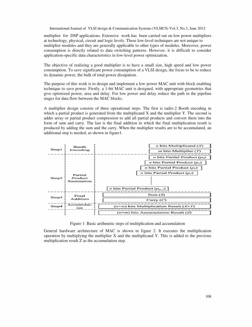
A multiplier design consists of three operational steps. The first is radix-2 Booth encoding in
which a partial product is generated from the multiplicand X and the multiplier Y. The second is
adder array or partial product compression to add all partial products and convert them into the
form of sum and carry. The last is the final addition in which the final multiplication result is
produced by adding the sum and the carry. When the multiplier results are to be accumulated, an
additional step is needed, as shown in figure1.
Figure 1: Basic arithmetic steps of multiplication and accumulation
General hardware architecture of MAC is shown in figure 2. It executes the multiplication
operation by multiplying the multiplier X and the multiplicand Y. This is added to the previous
multiplication result Z as the accumulation step.

International Journal of VLSI design & Communication Systems (VLSICS) Vol.3, No.3, June 2012
109
Figure 2: Hardware Architecture of general MAC Array Multiplier
A 4 x 4 array multiplier and the functions of M0, M1, M2, and M4 (M’s are either half adders or
full adders) are shown in figure 3. X3X2X1X0 is the 4 bit multiplicand and Y3Y2Y1Y0 is the 4 bit
multiplier.
Full adder is the important component in each cell. Each cell consist of AND gate, which
determines whether a multiplicand bit, Xj is added to the incoming partial product bit based on
the value of the multiplier bit Yi. PPi is unchanged and passed vertically downward if Yi=0,else
each row adds the multiplicand (appropriately shifted) to the incoming partial product, PPi to
generate the outgoing partial product PP (i+1). The path from the upper right corner of the array to
the high order product bit output at the bottom left corner of the array is the worst case signal
propagation delay
Figure 3: A 4 x 4 Array Multiplier

International Journal of VLSI design & Communication Systems (VLSICS) Vol.3, No.3, June 2012
110
Booth's algorithm, given below, involves repeatedly adding one of two predetermined values A
and S to a product P, then performing a rightward arithmetic shift on P. Let X and Y be the
multiplicand and multiplier, respectively; and let m and r represent the number of bits in X and Y.
1. Determine the values of A and S, and the initial value of P. All of these numbers should have a
length equal to (m +r + 1).
(a) A: Fill the most significant (leftmost) bits with the value of X. Fill the remaining (r + 1)
bits with zeros.
(b) S: Fill the most significant bits with the value of (−X) in two's complement notation. Fill
the remaining (r + 1) bits with zeros.
(c) P: Fill the most significant m bits with zeros. To the right of this, append the value of Y.
Fill the least significant (rightmost) bit with a zero.
2. Determine the two least significant (rightmost) bits of P. If they are
(a) 01, find the value of P + A. Ignore any overflow.
(b) 10 find the value of P + S. Ignore any overflow.
(c) 00 do nothing. Use P directly in the next step.
(d) 11 do nothing. Use P directly in the next step.
3. Arithmetically shift the value obtained in the second step by a single place to the right. Let P
now equal this new value.
4. Repeat steps 2 and 3 for r number of times.
5. Drop the least significant (rightmost) bit from P. The result is the product of X and Y.
2. IMPLEMENTATION
The low power multiplier with SPST consists of i) modified Booth Encoder, ii) detection Unit,
and
iii) Register as shown in figure 4.
Figure 4: Proposed low power SPST equipped multiplier
Radix-2 modified booth MAC with SPST performs both multiplication and accumulation.
Multiplication result is obtained by multiplying multiplicand and multiplier. This multiplication
result is accumulated with previous result. The black box view of radix-2 modified Booth MAC
with SPST module is shown in figure 5.

International Journal of VLSI design & Communication Systems (VLSICS) Vol.3, No.3, June 2012
111
Figure 5: MAC with SPST module
3. MODIFIED BOOTH ENCODER
Modified Booth algorithm has been proposed for high speed multiplication .This type of
multiplier operates much faster than an array multiplier for longer operands because its
computation time is proportional to the logarithm of the word length of operands. Booth
multiplication is a technique that allows faster multiplication by grouping the multiplier bits. The
grouping of multiplier bits and Radix-2 Booth encoding reduce the number of partial products to
half. So we take every second column, and multiply by ±1, ±2, or 0, instead of shifting and
adding for every column of the multiplier term and multiplying by 1 or 0.The advantage of this
method is halving of the number of partial products. For Booth encoding the multiplier bits are
formed in blocks of three, such that each block overlaps the previous block by one bit. Start from
the LSB for grouping, and the first block only uses two bits of the multiplier. Figure 6 shows the
grouping of bits from the multiplier term.
Figure 6: Grouping of bits from the multiplier term
To obtain the correct partial product each block is decoded. Table 1 shows the encoding of the
multiplier Y, using the modified Booth algorithm, generates the following five signed digits, -2, -
1, 0, +1, +2. Each encoded digit in the multiplier performs a certain operation on the multiplicand
X.
Table 1: Operations on the multiplicand
4. SPURIOUS POWER SUPPRESSION TECHNIQUES AND REGISTER
Spurious transitions (also called glitches) in combinational CMOS logic are a well known source
of unnecessary power dissipation. Reducing glitch power is a highly desirable target because in
the vast majority of digital CMOS circuits, only one signal transition per clock cycle is
functionally meaningful. Unfortunately, glitch power is heavily dependent on the low-level
implementation details, namely, gate propagation delays and input transitions misalignments. The
procedure for glitch minimization is based on a well known idea. Glitches are eliminated by

International Journal of VLSI design & Communication Systems (VLSICS) Vol.3, No.3, June 2012
112
adding some redundant logic that prevents spurious transitions. This can be done by inserting
latches in a gate-level net list.
Figure 7 shows a 16-bit adder/subtractor based on the proposed SPST. In this, the 16-bit adder /
subtractor is divided into MSP (Most Significant Part) and LSP (Least Significant Part) between
the 8th and 9
th bits. The MSP of the original adder is modified to include detection logic circuits,
data controlling circuits, sign extension circuits, logic for calculating carry-in and carry-out
signals.
Simple logic gates are used to implement the latches and the sign extension circuits in order to
reduce the additional overhead as for as possible. Low power adder/subtractor consists of i)
latch,
ii) Detection logic, and iii) sign extension logic.
Figure 7: Low-power adder design using SPST
(a) Detection Logic
The most important part of detection logic is design of the control signal asserting circuit, shown
in figure 7. Although this asserting circuit brings evident power reduction, it may induce
additional delay. An approach for implementing the control signal assertion circuit is using
registers and is illustrated as shaded area in figures 9 and 10.

International Journal of VLSI design & Communication Systems (VLSICS) Vol.3, No.3, June 2012
113
Figure 8: Detection logic circuit using registers to assert the control signals
Figure 9: Detection logic circuit using AND gates to assert the control signals
(b) Applying SPST to the Modified Booth Encoder
The SPST equipped modified Booth encoder, which is controlled by a detection unit. One of the
two operands as input to the detection unit, which decide whether the Booth encoder calculates
redundant computations. As shown in Figure 10, the latches can, respectively, freeze the inputs of
MUX-4 to MUX-7 or only those of MUX-6 to MUX-7 when PP4 to PP7 or PP6 to PP7 are zero, to
reduce the transition power dissipation.

International Journal of VLSI design & Communication Systems (VLSICS) Vol.3, No.3, June 2012
114
Figure 10: SPST equipped modified Booth encoder
5. ARRAY MULTIPLIER AND ACCUMULATOR
A 4x4 array multiplier consists of 16 AND gates, 4 HAs, 8FAs (total 12 Adders) is shown in
figure 11.Therefore, for an m x n Array Multiplier, m*n AND gates, n HAs, (m-2)*n FAs, i.e. a
total of (m-1)*n adders are required. Figure 13 also illustrates generation of partial products in a
4x4 array multiplier. A total of 8 partial products are generated by the 4x4 array multiplier.
Similarly, a 16 x16 array multiplier takes 16- bit multiplicand and 16- bit multiplier and generates
32 partial products.
Figure 11: A 4x4 array multiplier
Array MAC performs both multiplication and accumulation. Multiplication result is obtained by
multiplying 16 -bit multiplicand and 16- bit multiplier. The result is accumulated with previous
result. Figure 12 shows array MAC module.

International Journal of VLSI design & Communication Systems (VLSICS) Vol.3, No.3, June 2012
115
Figure 12: Array MAC module
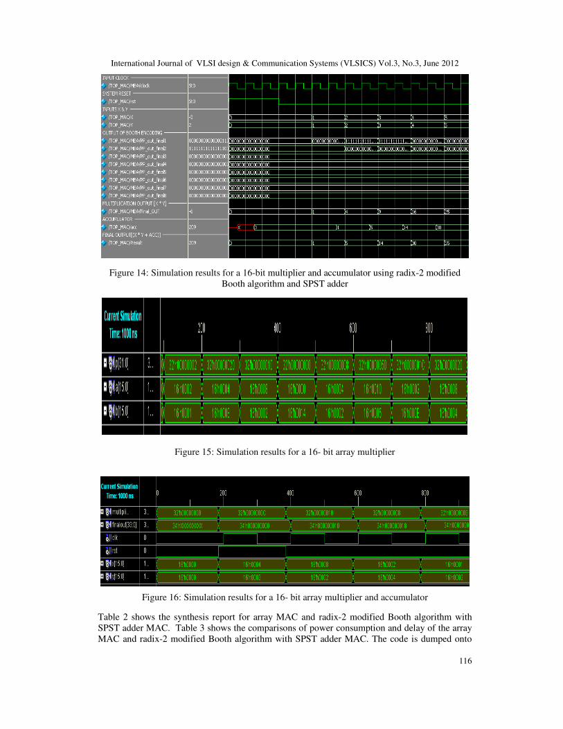
6. RESULTS
The simulation results for 16-bit Radix-2 modified Booth algorithm with SPST adder multiplier
and MAC are shown in figures 13 and 14 respectively. The simulation results for 16-bit array
multiplier and MAC are shown in figures 15 and 16 respectively.
.
Figure 13: Simulation results for a 16-bit multiplier using radix-2 modified Booth algorithm with
SPST adder
International Journal of VLSI design & Communication Systems (VLSICS) Vol.3, No.3, June 2012
116
Figure 14: Simulation results for a 16-bit multiplier and accumulator using radix-2 modified
Booth algorithm and SPST adder
Figure 15: Simulation results for a 16- bit array multiplier
Figure 16: Simulation results for a 16- bit array multiplier and accumulator
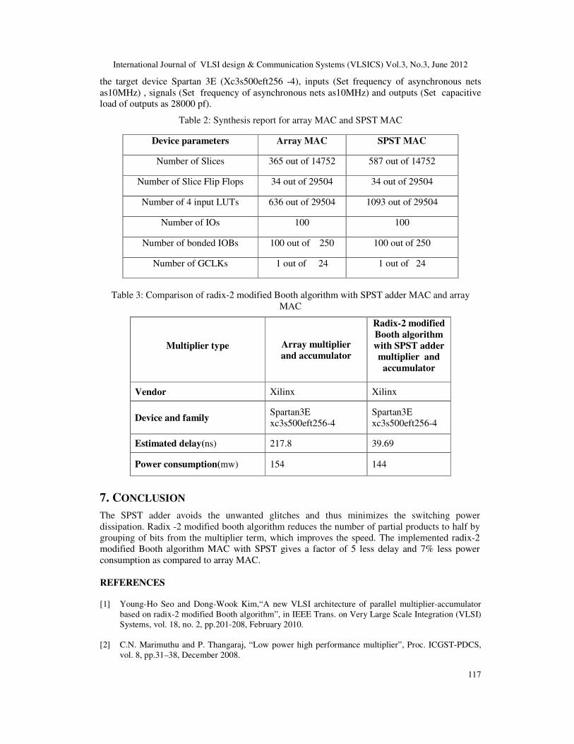
Table 2 shows the synthesis report for array MAC and radix-2 modified Booth algorithm with
SPST adder MAC. Table 3 shows the comparisons of power consumption and delay of the array
MAC and radix-2 modified Booth algorithm with SPST adder MAC. The code is dumped onto
International Journal of VLSI design & Communication Systems (VLSICS) Vol.3, No.3, June 2012
117
the target device Spartan 3E (Xc3s500eft256 -4), inputs (Set frequency of asynchronous nets
as10MHz) , signals (Set frequency of asynchronous nets as10MHz) and outputs (Set capacitive
load of outputs as 28000 pf).
Table 2: Synthesis report for array MAC and SPST MAC
Device parameters Array MAC SPST MAC
Number of Slices 365 out of 14752 587 out of 14752
Number of Slice Flip Flops 34 out of 29504 34 out of 29504
Number of 4 input LUTs 636 out of 29504 1093 out of 29504
Number of IOs 100 100
Number of bonded IOBs 100 out of 250 100 out of 250
Number of GCLKs 1 out of 24 1 out of 24
Table 3: Comparison of radix-2 modified Booth algorithm with SPST adder MAC and array
MAC
Multiplier type Array multiplier
and accumulator
Radix-2 modified
Booth algorithm
with SPST adder
multiplier and
accumulator
Vendor Xilinx Xilinx
Device and family Spartan3E
xc3s500eft256-4
Spartan3E
xc3s500eft256-4
Estimated delay(ns) 217.8 39.69
Power consumption(mw) 154 144
7. CONCLUSION
The SPST adder avoids the unwanted glitches and thus minimizes the switching power
dissipation. Radix -2 modified booth algorithm reduces the number of partial products to half by
grouping of bits from the multiplier term, which improves the speed. The implemented radix-2
modified Booth algorithm MAC with SPST gives a factor of 5 less delay and 7% less power
consumption as compared to array MAC.
REFERENCES
[1] Young-Ho Seo and Dong-Wook Kim,“A new VLSI architecture of parallel multiplier-accumulator
based on radix-2 modified Booth algorithm”, in IEEE Trans. on Very Large Scale Integration (VLSI)
Systems, vol. 18, no. 2, pp.201-208, February 2010.
[2] C.N. Marimuthu and P. Thangaraj, “Low power high performance multiplier”, Proc. ICGST-PDCS,
vol. 8, pp.31–38, December 2008.

International Journal of VLSI design & Communication Systems (VLSICS) Vol.3, No.3, June 2012
118
[3] K.H.Chen, Y.M.Chen, and Y.S.Chu, “A versatile multimedia functional unit design using the
spurious power suppression technique”, in Proc. IEEE Asian Solid-State Circuits Conf., 2006,
pp.111–114.
[4] G. Lakshmi Narayanan and B. Venkataramani, “Optimization techniques for FPGA -based wave
pipelined DSP blocks”, IEEE Trans. Very Large Scale Integration (VLSI) Systems, vol.13, no. 7,
pp.783-792, July 2005.
[5] K.H.Chen, K.C.Chao, J.I.Guo, J.S.Wang and Y.S. Chu, “An efficient spurious power suppression
technique (SPST) and its applications on MPEG-4 AVC/H.264 transform coding design”, Proc. IEEE
Int. Symps. Low Power Electron. Des., pp.155–160, 2005.
[6] P.Zicari, S.Perri, P.Corsonello and G.Cocorullo, “An optimized adder accumulator for high speed
MACs”, Proc. ASICON 2005, vol.2, pp.757–760, 2005.
[7] Z. Huang and M. D.Ercegovac, “High-performance low-power left-to right array multiplier design”,
IEEE Trans.Comput.,vol.54, no.3, pp.272–283, March 2005.
[8] H. Lee, “A power-aware scalable pipelined Booth multiplier”, Proc. IEEE Int. SOC Conf., , pp.123–
126, 2004.
[9] A. Fayed and M. Bayoumi, “A merged multiplier-accumulator for high speed signal processing
applications”, Proc. ICASSP, vol. 3, pp.3212–3215, 2002.
[10] J.Choi, J. Jeon and K.Choi,“Power minimization of functional units by partially guarded
computation”, Proc. IEEE Int. Symp. Low Power Electron. Des., pp. 131–136, 2000.
[11] L.Benini, G.D.Micheli, A.Macii, E.Macii, M.Poncino, and R.Scarsi, “Glitching power minimization
by selective gate freezing”, IEEE Trans. Very Large Scale Integration (VLSI) Systems, vol.8, no.3,
pp.287–297, June2000.
[12] F. Elguibaly, “A fast parallel multiplier–accumulator using the modified Booth algorithm”, IEEE
Trans. Circuits Syst., vol. 27, no. 9, pp.902–908, September 2000.
[13] J. Fadavi-Ardekani, “M*N Booth encoded multiplier generator using optimized Wallace trees”, IEEE
Trans. Very Large Scale Integration (VLSI) Systems, vol. 1, no. 2, pp. 120–125, June1993.
[14] A. R. Cooper, “Parallel architecture modified Booth multiplier”,Proc.Inst.Electr.Eng.G, vol.135,
pp.125–128, 1988.