International Journal of VLSI design & Communication...
17
International Journal of VLSI design & Communication Systems (VLSICS) Vol.3, No.5, October 2012 DOI : 10.5121/vlsic.2012.3508 93 DESIGN AND IMPLEMENTATION OF ANALOG MULTIPLIER WITH IMPROVED LINEARITY Nandini A.S 1 , Sowmya Madhavan 2 and Dr Chirag Sharma 3 1 Department of Electronics and Communication Engineering, Nitte Meenakshi Institute of Technology, Yelahanka, Bangalore- 560064 [email protected] 2 Department of Electronics and Communication Engineering, Nitte Meenakshi Institute of Technology, Yelahanka, Bangalore- 560064 [email protected] 3 Department of Electronics and Communication Engineering, Nitte Meenakshi Institute of Technology, Yelahanka, Bangalore- 560064 [email protected] ABSTRACT Analog multipliers are used for frequency conversion and are critical components in modern radio frequency (RF) systems. RF systems must process analog signals with a wide dynamic range at high frequencies. A mixer converts RF power at one frequency into power at another frequency to make signal processing easier and also inexpensive. A fundamental reason for frequency conversion is to allow amplification of the received signal at a frequency other than the RF, or the audio, frequency. This paper deals with two such multipliers using MOSFETs which can be used in communication systems. They were designed and implemented using 0.5 micron CMOS process. The two multipliers were characterized for power consumption, linearity, noise and harmonic distortion. The initial circuit simulated is a basic Gilbert cell whose gain is fairly high but shows more power consumption and high total harmonic distortion. Our paper aims in reducing both power consumption and total harmonic distortion. The second multiplier is a new architecture that consumes 43.07 percent less power and shows 22.69 percent less total harmonic distortion when compared to the basic Gilbert cell. The common centroid layouts of both the circuits have also been developed. KEYWORDS Multiplier, Gilbert cell, Noise spectral density, Total Harmonic Distortion, Transconductance 1. INTRODUCTION An Analog multiplier is a device having two input ports and an output port. The signal at the output is the product of the two input signals. If both input and output signals are voltages, the transfer characteristic is the product of the two voltages divided by a scaling factor, K, which has the dimension of voltage as shown in Figure 1 [1]. Figure 1. Basic Analog multiplier
Transcript of International Journal of VLSI design & Communication...

International Journal of VLSI design & Communication Systems (VLSICS) Vol.3, No.5, October 2012
DOI : 10.5121/vlsic.2012.3508 93
DESIGN AND IMPLEMENTATION OF ANALOG
MULTIPLIER WITH IMPROVED LINEARITY
Nandini A.S1, Sowmya Madhavan
2 and Dr Chirag Sharma
3
1Department of Electronics and Communication Engineering, Nitte Meenakshi Institute
of Technology, Yelahanka, Bangalore- 560064
[email protected] 2Department of Electronics and Communication Engineering, Nitte Meenakshi Institute
of Technology, Yelahanka, Bangalore- 560064
[email protected] 3Department of Electronics and Communication Engineering, Nitte Meenakshi Institute
of Technology, Yelahanka, Bangalore- 560064 [email protected]
ABSTRACT
Analog multipliers are used for frequency conversion and are critical components in modern radio
frequency (RF) systems. RF systems must process analog signals with a wide dynamic range at high
frequencies. A mixer converts RF power at one frequency into power at another frequency to make signal
processing easier and also inexpensive. A fundamental reason for frequency conversion is to allow
amplification of the received signal at a frequency other than the RF, or the audio, frequency. This paper
deals with two such multipliers using MOSFETs which can be used in communication systems. They were
designed and implemented using 0.5 micron CMOS process. The two multipliers were characterized for
power consumption, linearity, noise and harmonic distortion. The initial circuit simulated is a basic Gilbert
cell whose gain is fairly high but shows more power consumption and high total harmonic distortion. Our
paper aims in reducing both power consumption and total harmonic distortion. The second multiplier is a
new architecture that consumes 43.07 percent less power and shows 22.69 percent less total harmonic
distortion when compared to the basic Gilbert cell. The common centroid layouts of both the circuits have
also been developed.
KEYWORDS
Multiplier, Gilbert cell, Noise spectral density, Total Harmonic Distortion, Transconductance
1. INTRODUCTION
An Analog multiplier is a device having two input ports and an output port. The signal at the
output is the product of the two input signals. If both input and output signals are voltages, the
transfer characteristic is the product of the two voltages divided by a scaling factor, K, which has
the dimension of voltage as shown in Figure 1 [1].
Figure 1. Basic Analog multiplier

International Journal of VLSI design & Communication Systems (VLSICS) Vol.3, No.5, October 2012
94
Mixer is a device used to mix two input signals and deliver an output voltage at frequencies equal
to the difference or sum of the input frequencies. Any nonlinear device can do the job of mixing
or modulation, but it often needs a frequency selection network which is normally composed as a
LC network. Hence a mixer needs at least one non-linearity, such as multiplication or squaring, in
its transfer function. Every analog multiplier can effectively used as a mixer, but the inverse does
not hold [2].
There is a lot of similarity between multiplier and mixer, but the main difference between them is
that in frequency multiplier only one signal is implied while in mixer we need two signals as
source. The similarity is that, in both of them, we drive circuits to nonlinear region to produce the
harmonic of input signal in multiplier and to produce the intermodulation of input signals in
mixer. That is, in a mixer, there is a sum and difference of the input frequencies due to the non-
linearity of a device.
2. MIXER DEFINITIONS
Mixers are non-linear devices used in systems to translate one frequency to another. All mixer
types work on the principle that a large Local Oscillator (LO) RF drive will cause
switching/modulating the incoming Radio Frequency (RF) to the Intermediate Frequency (IF) [3].
The multiplication process begins by taking two signals:
a = Asin(ω1.t + φ1 ) and signal b = Bsin(ω2.t + φ2 ) (1)
The resulting multiplied signal will be:
a.b = AB sin(ω1.t + φ1 ). sin(ω2.t + φ2 ) (2)
This can be multiplied out thus:
Using the trigonometric identity
sinAsinB = -½[cos(A+B)-cos(A-B)] (3)
Where A = (ω1.t + φ1 ) and B = (ω2.t + φ2 )
= -AB/2 [cos((ω1.t +φ1 )+(ω2.t + φ2 ))
- cos((ω1.t + φ1 )-(ω2.t + φ2 ))] (4)
= -AB/2 [cos((ω1 + ω2 )t + (φ1+ φ2 ))
- cos((ω1 - φ1 )t - (φ1- φ2 ))] (5)
= -AB/2 [cos((ω1 + ω2 )t + (φ1+ φ2 )) - cos((ω1 – ω2 )t - (φ1- φ2 ))]
The following parameters are important for an analog multiplier.
(1) Conversion Gain: This is the ratio in dB between the IF signal which is the difference
frequency between the RF and LO signals and the RF signal.
(2) Noise Figure: Noise figure is defined as the ratio of SNR(Signal to Noise Ratio) at the IF port
to the SNR of the RF port.

International Journal of VLSI design & Communication Systems (VLSICS) Vol.3, No.5, October 2012
95
3. GILBERT CELL MIXER
The basic idea of multiplier implementation is illustrated in Figure 2 [4]. Two signals V1(t) and
V2(t) are applied to a non linear device, which can be characterized by a higher order polynomial
function. This polynomial function generates the terms like V1² (t), V2² (t), V1³ (t), V2³ (t), V1²
(t)*V2(t) and many others besides the desired V1(t).V2(t). Then it is required to cancel the
undesired components. This is accomplished by a cancellation circuit configuration.
A multiplier could be realized using programmable transconductance components. Consider the
conceptual transconductance amplifier of Figure 3(a), where the output current is simply given by
i0 = Gm1v1 (6)
Figure 2. Basic idea of multiplier.
where
Gm1 = Gm1 (Ibias1) (7)
For a bipolar transconductor, Gm1 becomes
Gm1 = Ibias1/(2.Vt ) (8)
Where Vt is the thermal voltage (kT/q).
Next, a small signal is added to the bias current as shown in Figure 3(b). The second input signal
v2(t)can be converted into a current, i2(t) = Gm2v2(t), as illustrated in Figure 3(c).
Then, the output current yields
i0(t) = Gm1v1 =
t
mbias
v
tvGI
2
)(221 +
. V1(t) (9)
i0(t) = )(22
)()(1
1212 tvv
I
v
tvtvG
t
bias
t
m+
= t
bias
tt
bias
v
tvI
vv
tvtvI
2
)(
2.2
)()( 11212+ (10)
or
i0(t) = )()()( 12211 tvktvtvk + (11)
Thus, i0(t) represents the multiplication of two signals v1(t) and v2(t) and an unwanted component
k2v1(t) [4]. This component can be eliminated as shown in Figure 3(d). Better cancellation is
achieved when the third transconductor (Gm2) becomes a fully differential transconductor, and v1
and v2 are fully differential inputs as illustrated in Figure 3(e).
i0(t) = )()(2 211 tvtvk (12)
International Journal of VLSI design & Communication Systems (VLSICS) Vol.3, No.5, October 2012
96
This is the basic operation principle of a Gilbert cell [5], [6]. Operational transconductance
amplifier (OTA)-based implementations are reported in [8]–[9]. The connection to the Gilbert cell
can be seen by substituting the transconductors in Figure 3(e) by bipolar junction transistor (BJT)
differential pairs.
As the digital technology dominates in modern electronics, analog circuits are required to share
the same standard CMOS process for low-cost fabrication. Thus, the popular BJT Gilbert Cell is
not suitable in a standard digital process, and designers must address low power supply voltage
requirements. One problem that circuit designers often encounter is how to select the best
multiplier architecture for their applications. Unfortunately, designers who propose multipliers in
the literature often do not make reference to or comparison to other multipliers. This lack of
comparison causes the same basic multiplier architectures to be, from time to time, reported as
“new” architectures. The transconductance multipliers are classified into eight types. They can be
categorized into two groups based on its MOS operating region, linear and saturation. It should be
emphasized that the fundamental multiplier circuit topology for many of the multipliers is the
same [4].
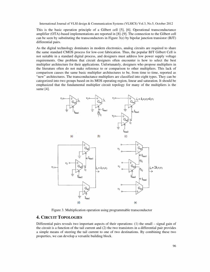
4. CIRCUIT TOPOLOGIES
Differential pairs reveals two important aspects of their operations: (1) the small – signal gain of
the circuit is a function of the tail current and (2) the two transistors in a differential pair provides
a simple means of steering the tail current to one of two destinations. By combining these two
properties, we can develop a versatile building block.
Figure 3. Multiplication operation using programmable transconductor

International Journal of VLSI design & Communication Systems (VLSICS) Vol.3, No.5, October 2012
97
Suppose we wish to construct a differential pair whose gain is varied by a control voltage. This
can be accomplished as depicted in Figure 4(a), where the control voltage defines the tail current
and hence the gain. In this topology, the voltage gain varies from zero to a maximum value given
by voltage headroom limitations and device dimensions. This circuit is a simple example of a
“variable – gain amplifier” (VGA) [10]. VGAs find application in systems where the signal
amplitude may experience large variations and hence requires inverse changes in the gain.
Now suppose we seek an amplifier whose gain can be continuously varied from a negative value
to a positive value. For that we consider two differential pairs that amplify the input by opposite
gains Figure 4(b). We now have
Vout1/Vin = -gmRD (13)
and Vout2/Vin = +gmRD (14)
where gm denotes the transconductance of each transistor in equilibrium. If I1 and I2 vary in
opposite directions, then we have two gain values inout vv /1 and inout vv /2 which vary in
opposite directions.
We can combine Vout1 and Vout2 into a single output as shown in Fig 5(a) then the two voltages
can be summed, producing
Vout = Vout1 + Vout2 = inin VAVA .. 21 + (15)
Where A1 and A2 are controlled by Vcont1 and Vcont2 respectively.
Since 211 DDDDout IRIRV −= (16)
342 DDDDout IRIRV −= (17)
We have,
).()( 324121 DDDDDDoutout IIRIIRVV +−+=+ (18)
Thus, rather than add Vout1 and Vout2, we can short the corresponding drain terminals to sum the
currents and subsequently generate the output voltage. If I1 =0 then Vout = gmRDVin and if I2 =0,
then Vout = -gmRDVin. For I1 = I2 the gain drops to zero. In the circuit of Figure 5(b), Vcont1 and
Vcont2 must vary I1 and I2 in opposite directions such that the gain of the amplifier changes
monotonically [10]. For a large 21 contcont vv − all of the tail current is steered to one of
Figure 4. (a) Simple VGA. (b) two stages providing opposite gains.

International Journal of VLSI design & Communication Systems (VLSICS) Vol.3, No.5, October 2012
98
\
the top differential pairs and the gain from Vin to Vout is at its most positive or most negative
value. For Vcont1 = Vcont2, the gain is zero. For simplicity, we redraw the circuit as shown in Fig
5(d) which is called as “Gilbert cell”. The idea is to convert the input voltage to current by means
of M5 and M6 and route the current through M1 –M4 to the output nodes. If the voltage given to
M1 and M3 is positive, then only M1 and M2 are on.
inDmout VRgV 6,5= (19)
Similarly if the voltage given to M4 and M2 is negative then only M3 and M4 are on.
inDmout VRgV 6,5−= (20)
Table 1. Specifications for Multiplier Design
VDD = 5V Noise spectral
density <1µV/Rt
Conversion gain
> 10dB
Power < 1mW Frequency of
operation
>100MHz
Dynamic Range
> 100dB
Figure 5. (a) Summation of the output voltages of two amplifiers, (b) summation in the current
domain, (c) use of M5- M6 to control the gain, (d) Gilbert cell
International Journal of VLSI design & Communication Systems (VLSICS) Vol.3, No.5, October 2012
99
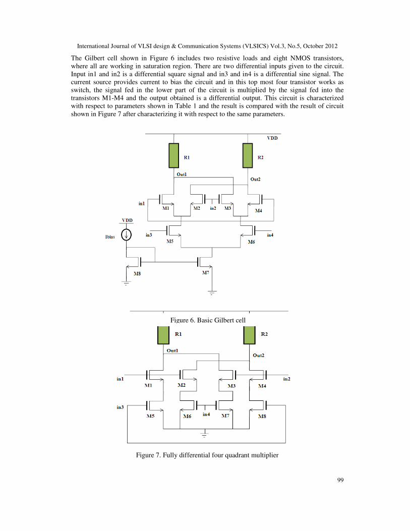
The Gilbert cell shown in Figure 6 includes two resistive loads and eight NMOS transistors,
where all are working in saturation region. There are two differential inputs given to the circuit.
Input in1 and in2 is a differential square signal and in3 and in4 is a differential sine signal. The
current source provides current to bias the circuit and in this top most four transistor works as
switch, the signal fed in the lower part of the circuit is multiplied by the signal fed into the
transistors M1-M4 and the output obtained is a differential output. This circuit is characterized
with respect to parameters shown in Table 1 and the result is compared with the result of circuit
shown in Figure 7 after characterizing it with respect to the same parameters.
Figure 6. Basic Gilbert cell
Figure 7. Fully differential four quadrant multiplier

International Journal of VLSI design & Communication Systems (VLSICS) Vol.3, No.5, October 2012
100
Table 2. Circuit Elements
Parameter Name Basic Gilbert cell Fully Differential four
quadrant multiplier
R1
R2
Ibias
Device Name
M1
M2
M3
M4
M5
M6
M7
70k
70k
14µ A
W/L
4
4
4
4
8
8
16
70k
70k
-
W/L
8
8
8
8
8
8
8
M8 4 8
5. SIMULATION RESULTS AND
PART A: The simulation results for the basic multiplier are discussed next. Each parameter is
numbered for clarity of the overall characterization.
1. Transient analysis for the basic multiplier which is in figure 6 is done. The output is as shown
in figure 8.
Figure 8.Transient Analysis of the Basic Gilbert cell multiplier

International Journal of VLSI design & Communication Systems (VLSICS) Vol.3, No.5, October 2012
101
The multiplier output from the simulation result in figure 8 is 1.55v.
This approximately equals to the output value got from equation 19.
Hence Conversion Gain = 20 log (vout/vin) (21)
= 23.80dB
2. Dynamic range = 20 log (vmax/vmin) (22)
= 187.23dB
Where vmax and vmin are maximum and minimum values of voltages given to test the output
of the multiplier.
3. Noise spectral density N0 is the noise power per unit of bandwidth; that is, it is the power
spectral density of the noise which has a dimension of power/frequency.
Figure 9. Noise spectral density of basic Gilbert cell multiplier
From figure 9, the noise spectral density is 36ηv/Rt.
4. The power consumption of the circuit is 325µW.
5. Total Harmonic Distortion, or THD is an amplifier or pre-amplifier specification that
compares the output signal of the amplifier with the input signal and measures the level
differences in harmonic frequencies between the two. The difference is called total harmonic
distortion. The maximum THD in percentage is 40.75% for an input voltage of 1.5V. The THD
plot is as shown in the Figure 10.

International Journal of VLSI design & Communication Systems (VLSICS) Vol.3, No.5, October 2012
102
Figure 10. THD plot of basic Gilbert cell multiplier
PART B: The simulation results for the fully Differential four quadrant multiplier are discussed
next. Each parameter is numbered for clarity of the overall characterization.
1. Transient analysis for the fully differential four quadrant multiplier is as shown in Figure 11.
Figure 11. Fully Differential four quadrant multiplier
The fully differential four quadrant multiplier output is 0.65v.
The conversion gain = 20 log (vout/vin) = 16.25dB.
2. Dynamic range = 20 log (vmax/vmin)
= 195.56dB
Where vmax and vmin are maximum and minimum values of voltages given to test the output
of the multiplier.

International Journal of VLSI design & Communication Systems (VLSICS) Vol.3, No.5, October 2012
103
3. The Noise spectral density is 590ηv/Rt for the fully differential multiplier as shown in figure
12.
Figure 12. Noise spectral density of Fully Differential multiplier
4. Power consumption of the Fully Differential multiplier is 185µW.
5. The maximum Total Harmonic Distortion in percentage is 18.06% for an input voltage of
1.5V. The THD plot is as shown in the Figure 13.
Figure 13. THD plot of Fully Differential four quadrant multiplier
Comparison of the results of Basic Gilbert cell multiplier and Fully differential four
quadrant multiplier is given in the Table 3.

International Journal of VLSI design & Communication Systems (VLSICS) Vol.3, No.5, October 2012
104
Table 3. Comparison of The Two Multipliers
This shows that the fully differential four quadrant multiplier is more linear and has less power
consumption as compared to basic Gilbert cell multiplier.
PART C: Comparison plots for power consumption and THD
1. The power consumption for the Basic Gilbert cell multiplier and fully differential four
quadrant multiplier are compared and is as shown in Figure 14.
Figure 14. Comparison graph of power consumption of figures (6) and (7).
2. The total harmonic distortion for the Basic Gilbert cell multiplier and fully differential
four quadrant multiplier are compared and is as shown in the Figure 15.
Parameter Name Basic Gilbert cell
multiplier
Fully Differential four
quadrant multiplier
Supply Voltage
Conversion gain
Dynamic range
Noise spectral
density
Frequency of
operation
5V
24.17dB
187.23dB
36 ηV/Rt
>100MHz
5V
16.25dB
195.56dB
590 ηV/Rt
>100MHz
Power consumption 325µW 185µW
Total harmonic
distortion for
1.5volt
40.75%
18.06%

International Journal of VLSI design & Communication Systems (VLSICS) Vol.3, No.5, October 2012
105
The goal of this work is to come with a multiplier architecture suitable for spread spectrum time
domain reflectometry (SSTDR) [7]. SSTDR requires a multiplier with wide linear range and low
power consumption. Fig 15 shows that fully differential four quadrant multiplier is much linear
compared to Gilbert cell multiplier.
5. LAYOUTS
Layouts are drawn for the Basic Gilbert cell multiplier both with IO padframe and without IO
padframe. In basic Gilbert cell multiplier, common centroid and fingering have been used and the
layout is as shown in Figure 16.
Figure 15. Comparison graph of THD of figures (6) and (7).
Figure 16. Common centroid layout of Basic Gilbert multiplier
International Journal of VLSI design & Communication Systems (VLSICS) Vol.3, No.5, October 2012
106
Area without IO pad = L * W
= 66.6µm * 43.2µm = 2877.12µm2
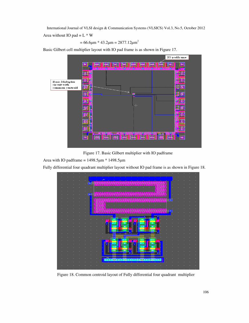
Basic Gilbert cell multiplier layout with IO pad frame is as shown in Figure 17.
Figure 17. Basic Gilbert multiplier with IO padframe
Area with IO padframe = 1498.5µm * 1498.5µm
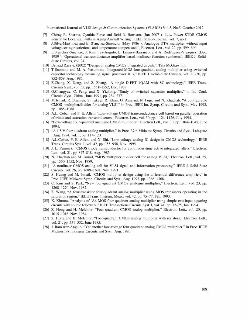
Fully differential four quadrant multiplier layout without IO pad frame is as shown in Figure 18.
Figure 18. Common centroid layout of Fully differential four quadrant multiplier

International Journal of VLSI design & Communication Systems (VLSICS) Vol.3, No.5, October 2012
107
Area without IO pad = L * W
= 72.6µm * 43.2µm = 3158.1µm2
Fully differential four quadrant multiplier layout with IO pad frame is as shown in Figure 19.
Figure 19. Fully differential four quadrant circuit with IO pad
For fully differential four quadrant multiplier, area with IO padframe is same as for the circuit
shown in Figure 17.
6. CONCLUSIONS
In this work new multiplier architecture was compared to the widely used Gilbert cell multiplier.
The goal of this work was to find a multiplier architecture with a wider linear range and lower
power consumption. The Total Harmonic Distortion for the basic Gilbert cell multiplier and the
fully differential four quadrant multiplier are 40.75% and 18.06% respectively. The power
consumption for the basic Gilbert cell multiplier and the fully differential four quadrant multiplier
are 325µW and 185µW respectively. Hence the proposed fully differential architecture has a
lower Total Harmonic Distortion and power consumption than a Gilbert cell multiplier without
much increase in chip area. Hence the fully differential four quadrant multiplier is better suited
for SSTDR system compared to widely used Gilbert cell multiplier.
REFERENCES
[1] Analog multipliers, “MT-079 Tutorial”, www.analog.com/static/imported-files/tutorials/MT079.pdf.
[2] www.edaboard.com/thread95080.html
[3] J.P. Silver, “Gilbert Cell Mixer Design Tutorial”, www.rfic.co.uk
[4] Gunhee Han, Sanchez Sinencio.E, (Dec 1998) “CMOS Transconductance Multipliers: A Tutorial”,
IEEE circuits and system society, vol 45 .
[5] B.Gilbert, (Dec.1968) “A precision four-quadrant multiplier with subnanosecond response,” IEEE J.
Solid-State Circuits, vol. SC-3, pp. 353–365.
[6] (Dec. 1974) “A high-performance monolithic multiplier using active feedback,” IEEE J. Solid-State
Circuits, vol. SC-9, pp. 364–373.
International Journal of VLSI design & Communication Systems (VLSICS) Vol.3, No.5, October 2012
108
[7] Chirag R. Sharma, Cynthia Furse and Reid R. Harrison, (Jan 2007 ) “Low-Power STDR CMOS
Sensor for Locating Faults in Aging Aircraft Wiring”, IEEE Sensors Journal, vol. 7, no.1.
[8] J.Silva-Mart´ınez and E. S´anchez-Sinencio, (May 1986 ),“Analogue OTA multiplier without input
voltage swing restrictions, and temperature compensated”, Electron. Lett., vol. 22, pp. 599–600.
[9] E.S´anchez-Sinencio, J. Ram´ırez-Angulo, B. Linares-Barranco, and A. Rodr´ıguez-V´azquez, (Dec.
1989 ) “Operational transconductance amplifier-based nonlinear function syntheses”, IEEE J. Solid-
State Circuits, vol. 24.
[10] Behzad Razavi, (2002) “Design of analog CMOS integrated circuits”, Tata McGraw hill.
[11] T.Enomoto and M. A. Yasumoto, “Integrated MOS four-quadrant analog multiplier using switched
capacitor technology for analog signal processor IC’s,” IEEE J. Solid-State Circuits, vol. SC-20, pp.
852–859, Aug. 1985.
[12] Z.Zhang, X. Dong, and Z. Zhang, “A single D-FET 4QAM with SC technology,” IEEE Trans.
Circuits Syst., vol. 35, pp. 1551–1552, Dec. 1988.
[13] O.Changyue, C. Peng, and X. Yizhong, “Study of switched capacitor multiplier,” in Int. Conf.
Circuits Syst., China , June 1991, pp. 234–237.
[14] M.Ismail, R. Brannen, S. Takagi, R. Khan, O. Aaserud, N. Fujii, and N. Khachab, “A configurable
CMOS multiplier/divider for analog VLSI,” in Proc. IEEE Int. Symp. Circuits and Syst., May 1993,
pp. 1085–1088.
[15] A.L. Coban and P. E. Allen, “Low-voltage CMOS transconductance cell based on parallel operation
of triode and saturation transconductors,” Electron. Lett., vol. 30, pp. 1124–1126, July 1994.
[16] “Low-voltage four-quadrant analogue CMOS multiplier,” Electron.Lett., vol. 30, pp. 1044–1045, June
1994.
[17] “A 1.5 V four quadrant analog multiplier,” in Proc. 37th Midwest Symp. Circuits and Syst., Lafayette
, Aug. 1994, vol. 1, pp. 117–120.
[18] A.L.Coban, P. E. Allen, and X. Shi, “Low-voltage analog IC design in CMOS technology,” IEEE
Trans. Circuits Syst. I, vol. 42, pp. 955–958, Nov. 1995.
[19] J. L. Pennock, “CMOS triode transconductor for continuous-time active integrated filters,” Electron.
Lett., vol. 21, pp. 817–818, Aug. 1985.
[20] N. Khachab and M. Ismail, “MOS multiplier divider cell for analog VLSI,” Electron. Lett., vol. 25,
pp. 1550–1552, Nov. 1989.
[21] “A nonlinear CMOS analog cell for VLSI signal and information processing,” IEEE J. Solid-State
Circuits, vol. 26, pp. 1689–1694, Nov. 1991.
[22] S. Huang and M. Ismail, “CMOS multiplier design using the differential difference amplifier,” in
Proc. IEEE Midwest Symp. Circuits and Syst., Aug. 1993, pp. 1366–1368.
[23] C. Kim and S. Park, “New four-quadrant CMOS analogue multiplier,” Electron. Lett., vol. 23, pp.
1268–1270, Nov. 1987.
[24] Z. Wang, “A four-transistor four-quadrant analog multiplier using MOS transistors operating in the
saturation region,” IEEE Trans. Instrum. Meas., vol. 42, pp. 75–77, Feb. 1993.
[25] K. Kimura, “Analysis of ‘An MOS four-quadrant analog multiplier using simple two-input squaring
circuits with source followers,” IEEE Transactions Circuits Syst. I, vol. 41, pp. 72–75, Jan. 1994.
[26] Z. Hong and H. Melchior, “Four-quadrant CMOS analog multiplier,” Electron. Lett., vol. 20, pp.
1015–1016, Nov. 1984.
[27] Z. Hong and H. Melchior, “Four-quadrant CMOS analog multiplier with resistors,” Electron. Lett.,
vol. 21, pp. 531–532, June 1985.
[28] J. Ram´ırez-Angulo, “Yet another low-voltage four quadrant analog CMOS multiplier,” in Proc. IEEE
Midwest Symposium Circuits and Syst., Aug. 1995.

International Journal of VLSI design & Communication Systems (VLSICS) Vol.3, No.5, October 2012
109
Authors
Nandini A S was born on 4th
November, 1987 in Bangalore. Nandini A S completed
her Bachelor of Engineering in Telecommunication Engineering from Vivekananda
Institute of Technology, Bangalore, Karnataka, India in 2009 and currently pursuing
Master of Technology from Nitte Meenakshi Institute of Technology, Bangalore,
Karnataka, India in VLSI Design and Embedded Systems.
Sowmya Madhavan was born on 26
th May, 1983 in Bangalore. Sowmya Madhavan
completed her Bachelor of Engineering in Telecommunication Engineering from
Vivekananda Institute of Technology, Bangalore, Karnataka, India in 2001 and Master
of Technology from AMC College of Engineering, Bangalore, Karnataka, India in
digital electronics and communication. She is currently pursuing her PhD under
Visvesvaraya Institute of Technology in low power VLSI design.
Chirag R. Sharma was born on 1st November, 1979. Chirag R Sharma received the
B.E. degree in electrical engineering from the Maharaja Sayajirao University, Baroda,
India, in 2001, and the M.S. degree in electrical and computer engineering from Utah
State University, Logan, in 2003. He also received the Ph.D. degree in electrical
engineering at the University of Utah, Salt Lake City in 2009.His current research
interests are analog and mixed-signal CMOS circuit design, CMOS sensors, and
reflectometry techniques for locating intermittent faults on aircraft wiring.