Estimation of Delay, Power, And Bandwidth for on-Chip VLSI Global Interconnects
38
Estimation of Delay, Power, and Bandwidth for On-Chip VLSI Global Interconnects Vikas Maheshwari M.Tech-Final Year (Microelectronics & VLSI) (08/ECE/455 ) Under the supervisions of Dr. Ashis Kumar Mal Mr. Rajib Kar Asst. Professor, ECE Deptt Asst. Professor, ECE Deptt N.I.T. Durgapur N.I.T. Durgapur
-
Upload
maheshwarivikas5735 -
Category
Documents
-
view
66 -
download
1
Transcript of Estimation of Delay, Power, And Bandwidth for on-Chip VLSI Global Interconnects

Estimation of Delay, Power, and Bandwidth for On-Chip VLSI Global Interconnects
Vikas MaheshwariM.Tech-Final Year (Microelectronics & VLSI)
(08/ECE/455 )
Under the supervisions of
Dr. Ashis Kumar Mal Mr. Rajib KarAsst. Professor, ECE Deptt Asst. Professor, ECE Deptt
N.I.T. Durgapur N.I.T. Durgapur

Content
Introduction
Moment Matching and Model Order Reduction
Interconnect Models
Distributed RC Tree Model
Distributed RLC Tree Model
Distributed RLCG Tree Model
Conclusion
Future Prospects
Publications
References

IntroductionInterconnection is a medium through which
signal propagates from point A to reach other points,such as B and C.In the nanotechnology age, as ultra deep sub-micron effects continue to wreak havoc on the integrity of the signal, so efficient and accurate computation of interconnect parameters has become critical.Due to the large number and complex nature of on-chip interconnects, the accurate estimation of the propagation delay in the interconnects is very important for the design of high speedVLSI systems.This work represents the analysis and parameters estimation of RC, RLC and RLCG interconnects. Topics covered in this work include on-chip interconnect delay , bandwidth, crosstalk and power modeling for different interconnect models.

Moment MatchingMoments of the impulse response are widely used for interconnectdelay analysis, from the explicit Elmore delay expression, to moment matching methods which creates reduced order trans-impedance and transfer function approximations.If more moments are required for an accurate approximation, moment matching or other order reduction schemes can be used to generate reduced-order dominant pole/zero approximations for the interconnect transfer, admittance, and impedance functions.Consider the simple RC ladder circuit shown in Figure 1 We can express the transfer function of this circuit as
Figure 1 Simple RC ladder Circuit
mm
nn
sbsbsbsasasaa
sVinsVoutsH
++++++++
==............................1
..........................)()()( 2
21
2210
where m>n

Expanding this equation about s = 0 we can rewrite the transfer function as a series in powers of s :
where the coefficients, mj’ s are known as circuit moments and can be shown as
It is straightforward to show that the first few central moments can be expressed in terms of circuit moments as follows
..........................................)( 33
2210 ++++= smsmsmmsH
( )∫∞−
=0
)(!
1 dtthtq
m qq
q
⎪⎪⎪
⎭
⎪⎪⎪
⎬
⎫
−+−=
−=
===
10
21
0
2133
0
21
22
1
00
26
6
2
01
mm
mmm
m
mm
m
m
µ
µ
µµ
µ0 is the area under the curve.
µ2 is variance of the distribution
µ3 is a measure of the skew ness
(1)
(2)
(3)
The aim of MOR is to perform the simulation and analysis on the reduced system instead of the original one in order to increase computational efficiency.
MOR is the technique that approximates the original large scale system with a smaller scale system without introducing much degradation of accuracy in both frequency and time domains.
Fig.2 demonstrates the general mechanism of MOR in a single-input single-output where r<<n such that the transfer function of the reduced-order system is approximated to that of the original one, i.e.,
Model Order Reduction
)(ˆ)( sGsG ≈
)(ˆ....................ˆˆ1
ˆ...........................ˆˆˆ)(ˆ
)(....................1
...........................)(
11
221
11
2210
11
221
11
2210
rordersystemreducedtheofFunctionTransfersbsasa
sbsbsbbsG
nordersystemoriginaltheofFunctionTransfersbsasa
sbsbsbbsG
rr
nn
rr
nn
−−
−−
−−
−−
++++
+++=
+++++++
=
Figure 2: MOR approximates the large scale original system of order n with a smaller scale system of order r.

Interconnect Models
On-chip global interconnect lines are modeled in three types as discussed bellow
Distributed RC Interconnect ModelDistributed RLC Interconnect ModelDistributed RLCG Transmission line Interconnect Model
Distributed RC interconnect models are of three types L, T, Π as shown in figure 3.
L-Type T-Type Π-Type

Distributed RC Tree ModelOn-chip VLSI interconnect is most often modelled by RC tree. The RCmodel is easy to compute, but relatively inaccurate. Figure 3 shows a typical RC tree.
Figure 4 An Interconnect and its electrical model
For a uniform structure with a rectangle cross-section the resistance is given by
⎟⎠⎞
⎜⎝⎛=
wlRR S
tRSρ=Where
l, t, and w are the resistivity, length, thickness, and width of the wire

For capacitance extraction many different techniques can be employed. Depending on the desired accuracy, these methods can vary from using very simple 2-D analytical models to employing 3-D electrostatic field solvers.
The simplest curve-fitting based model approximates the per-unit-length capacitance as
One conservative estimate for the number of lumped segments (N) required to model a URC, based on the maximum signal frequency of interest, is obtained by solving
⎥⎥⎦
⎤
⎢⎢⎣
⎡⎟⎠⎞
⎜⎝⎛+⎟
⎠⎞
⎜⎝⎛=
222.0
8.215.1ht
hwC ε
wCCC 10 +=
( )⎥⎦
⎤⎢⎣
⎡⎟⎠⎞
⎜⎝⎛ −−≤
NN
RCNf
212cos12 2
maxπ
(4)
(5)
(6)
(4)
(5)
Venue: N.I.T. Durgapur, W.B.
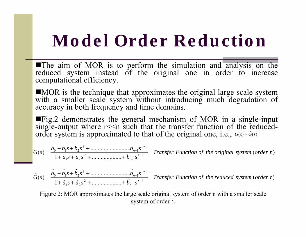
RC Delay Model Based on Gamma Distribution
Elmore assumed and therefore approximated the median (the desired delay) by the mean of the impulse response. The main idea behind our Delay metrics is to match the mean and variance of the impulse response to those of Gamma distribution.The Gamma distribution is a two parameter continuous distribution. It is well suited to match the impulse response of the generalized RC network since both are unimodel and have non-negative skewness.
The PDF of Burr’s distribution is shown in the following figure-5.
1mk −=
Figure 5 The Gamma Distribution Function

The probability density function of gamma distribution g λ, n (t), is a function of one variable t and two parameters λ and n
Gamma’s cumulative distribution function [CDF] as a function of t is given by
CDF must satisfy the following conditions
Calculation of Parameters of the Gamma Distribution FunctionMean and Variance of the Gamma function is given by
0,)(
)(1
, >Γ
=−−
tnettg
tnn
n
λ
λλ
0,)(0
1 >=Γ −∞
−∫ xdyeyx yxWhere
0 , 1)( >−=−
tethtλ
0)(,1)(1)(00
==≤≤→∞→
tFLimtFLimandtFtt
1mn−=
λ( )2
212 2mmn−−=
λ
(7)
(8) (9)

From (8) and (9),
Calculation of Median (50 % Delay) of the Gamma Distribution Function
Median of Gamma function is given by
Mode=3*Median-2* Mean
From (3.27) and (3.28),
221
21
221
1
2
2 mmmnand
mmm
−−
=−
=λ (10)
( )
⎪⎪⎭
⎪⎪⎬
⎫
⎥⎦⎤
⎢⎣⎡ −=⎥⎦
⎤⎢⎣⎡ −=
⎥⎦⎤
⎢⎣⎡ +
−=
+=
λλλλ
λλ
31 3/13
3/2132
nn
nnMeanModeMedian(11)
⎪⎪⎭
⎪⎪⎬
⎫
+=
⎟⎟⎠
⎞⎜⎜⎝
⎛ −−−=
1
21
1
221
1
32
34- %) (50Delay or,
32
mmm
mmm
mMedian(12)

Experimental Set-Up
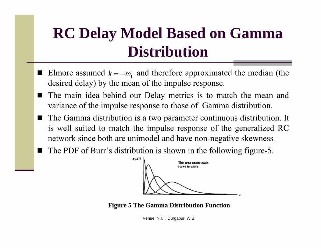
We have implemented the proposed delay estimation method using Gamma Distribution and applied it to widely used actual interconnect RC networks as shown in Figure6. For each RC network source we put a driver, where the driver is a voltage source followed by a resister.
We compare the delays obtained from SPICE with those found using our proposed model. The results for the 50% delay are summarized in Table 1.
(2) (4) (5)
(6) (7)
(1) (3)
60 ohm
1.2pF1pF
60 ohm
1.2pF
60 ohm
1pF
60 ohm
1pF
60 ohm60 ohm
1pF
+
-
Vin
0.5pF
80 ohm
Figure 6 An RC Tree Example
Experimental Result
0.4510.45270.3730.37560.9230.91950.8280.84540.6970.70030.4930.47720.2340.1961
Proposed Model (ns)SPICE (ns)Node
Table 1 Comparison of the 50% delays between SPICE and the Proposed Delay Metric (time in ns).

Distributed RLC Tree Model
Importance of On-Chip InductanceWith these technology trends, on-chip inductance effects, such as delay increase, overshoot, and inductive crosstalk, can no longer be ignored. Inductance effects have become increasingly significantbecause: As the clock frequency increases and the rise time decreases,
electrical signals comprise more and more high frequency components, making the inductance effect more significant.With the increase of chip size, it is fairly typical that many wires are long and run in parallel, which increases the inductive crosstalk.Due to the lack of highly conductive ground planes on the chips, the mutual coupling between the wires cover very long ranges and decrease very slowly with the increase of spacing.

Effect of InductanceA key aspect of RLC delay estimation is first controlling the damping, then approximating the delay. Excessive settling time increases delay in some sense, both under-damping and over-damping adversely impact delay. This is evidenced by the responses in Figure 7(b) for the series terminated RLC line in Figure 7(a).
Figure 7 (a) A source terminated RLC Transmission Line. (b) Response of the RLC system as RS4>RS3>RS2>RS1.
Power-Estimation using Model Order Reduction Technique
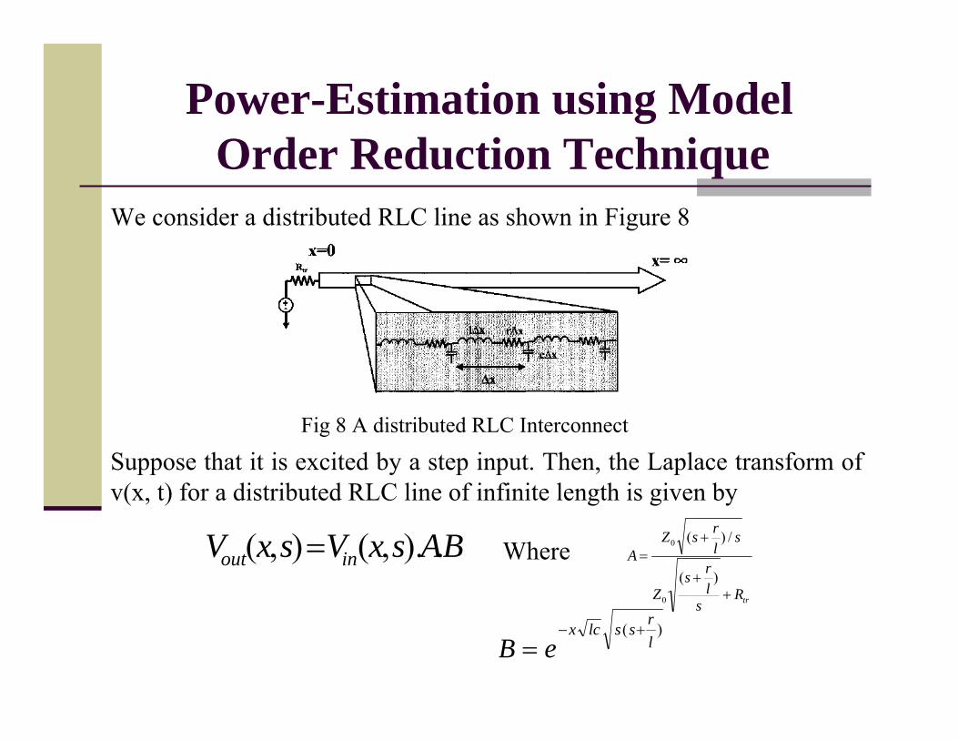
We consider a distributed RLC line as shown in Figure 8
Suppose that it is excited by a step input. Then, the Laplace transform of v(x, t) for a distributed RLC line of infinite length is given by
Fig 8 A distributed RLC Interconnect
BAsxVsxV inout .).,(),( =trR
slrs
Z
slrsZ
A
++
+=
)(
/)(
0
0Where
)(lrsslcx
eB+−
=
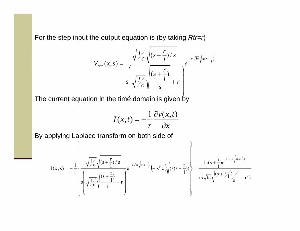
For the step input the output equation is (by taking Rtr=r)
The current equation in the time domain is given by
By applying Laplace transform on both side of
)(
)(
/)(),( l
rsslcx
out e
rs
lrs
cls
slrsc
lsxV
+−
⎟⎟⎟⎟
⎠
⎞
⎜⎜⎜⎜
⎝
⎛
++
+=
xtxv
rtxI
∂∂
−=),(1),(
( )srs
)lrs(
lcrs
e)lrs(lc
))lrs(s(lce
rs
)lrs(
cls
s/)lrs(c
l
r1)s,x(I
2
)lr
s(slcx -
)lr
s(slcx
++
+=
⎪⎪⎪⎪⎪
⎭
⎪⎪⎪⎪⎪
⎬
⎫
⎪⎪⎪⎪⎪
⎩
⎪⎪⎪⎪⎪
⎨
⎧
+−
⎟⎟⎟⎟
⎠
⎞
⎜⎜⎜⎜
⎝
⎛
++
+−=
+
+−

By equating the denominator term to zero, we get the pole of I(x, s) as
The pole P2 is in the left half of the s-plane, so we can write
The residue of I(x, s) at pole P2 is given by
Thus the energy dissipation at the arbitrary position is given by
221 0crlrPandP
−−==
2
2 )2(
22
2
2))2((
)2(),( crlcrlcr
xe
crlcrcrlcpxI −
−−
−+
−=−
2
2
222 ),()(limˆ crl
rcrx
psercsxIpsr −−
→=−=
2
2
2
2
2
crl
rc)crl2(crx
22
232
crl)crl2(cr
x
222
2crlrcrx2
2
e))crl2(cr(
)crl2(ccr
e))crl2(cr)(crl(
)crl2(ce.rcr
)p,x(Iresiduer)x(E
−
⎟⎠⎞⎜
⎝⎛ +−
−
−−
−−
−
−+
−×=
−+−
−××=
−××=
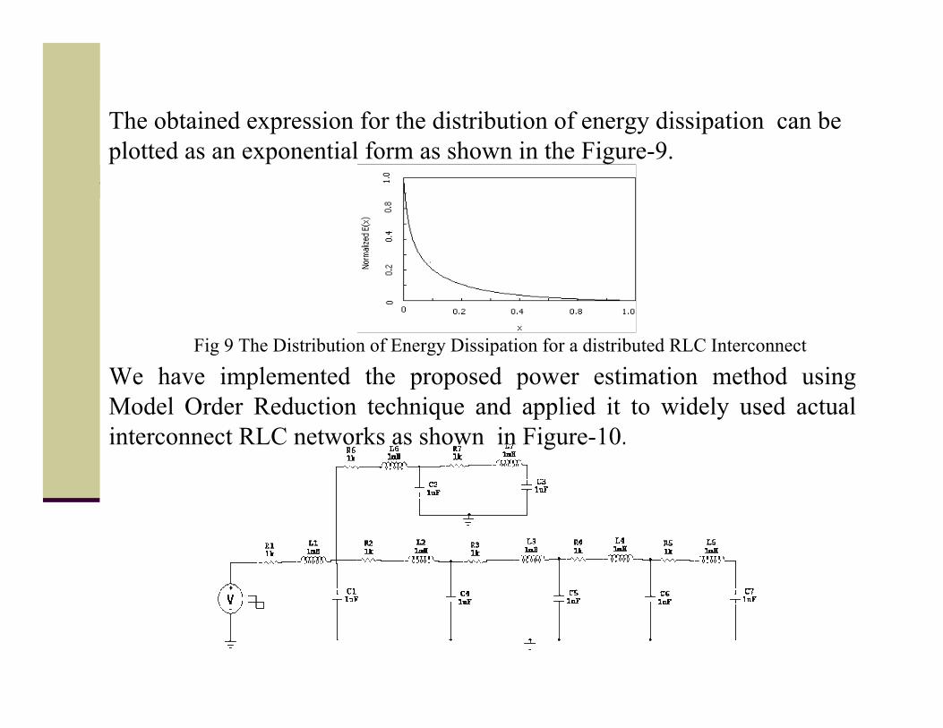
The obtained expression for the distribution of energy dissipation can be plotted as an exponential form as shown in the Figure-9.
We have implemented the proposed power estimation method using Model Order Reduction technique and applied it to widely used actual interconnect RLC networks as shown in Figure-10.
Fig 9 The Distribution of Energy Dissipation for a distributed RLC Interconnect

Table-2 gives the comparative result of the energy dissipation computed using SPICE and our method.
9.57X1051068.8X105106
9.35X1041058.5X104105
9.25X1031048.6X103104
9.2X1021038X102103
7958X1027008X102
5906X1025756X102
8510275100
10101019
8888
1111
0.20.20.20.2
Our Model (µJ)SPICE Model (µJ)Our Model (µJ)SPICE Model (µJ)
No of Nodes=1500No of Nodes=1000
Table-2 Comparison of the energy distribution for randomly generated RLC circuit

Figure-11 & Figure-12 show the graphical representation of the result for the circuit with 1000 and 1500 nodes respectively.
Fig-11. Comparison of the energy distribution for randomly generated RLC circuit with
1000 nodesFig-12. Comparison of the energy distribution
for randomly generated RLC circuit with 1500 nodes
Distributed RLCG Tree ModelIn case of very high frequency as in Giga scale (GHz), no longer can interconnects be treated as mere delays or lumped RC networks. The most common simulation model for interconnects is the distributed RLC model.In this case, the commonly and generally well-accepted Elmore delay calculation becomes inapplicable to RLC and RLCG interconnect networks due to their non-monotonic characteristics induced by inductances.Interconnect lines may be coupled to study the effects of mutualinductive and capacitive coupling.Our model considers both lossless components (i.e. L, C) and lossy components (i.e. R, G). The SPICE simulation justifies the accuracy of our proposed approach.

Transmission Line Model
An infinitesimal unit length of the transmission line looks like the circuit as shown in Figure 13. The parameters are defined as R, L, C and G is Series resistance, Series inductance, Shunt capacitance and Shunt conductance per unit length.
The following is a simple rule of thumb which can be used to determine when to use transmission line models.
Fig 13. RLCG parameters for a segment of a transmission
line.
ellinglumpedvl
ellinglumpedorlineontransmissieithervl
vl
ellinglineontransmissivl
fallrise
fallrise
fallrise
mod5)(
mod5)(5.2
mod5.2)(
⇒⎟⎠⎞
⎜⎝⎛×>
⇒⎟⎠⎞
⎜⎝⎛×<<⎟
⎠⎞
⎜⎝⎛×
−⇒⎟⎠⎞
⎜⎝⎛×<
ττ
ττ
ττ

Crosstalk
Crosstalk is undesired energy imparted to a transmission line due to signals in adjacent lines. The crosstalk noise between two shielded interconnects can produce a peak noise of 15% of VDD in a 0.18 um CMOS technology. In the complicated multilayered interconnect system, signal coupling and delay strongly affect circuit performances .
Major impacts of cross talk are: (I) Crosstalk induces delays, which change the signal propagation time, and thus may lead to setup or hold time failures.(II) Crosstalk induces glitches, which may cause voltage spikes on wire, resulting in false logic behaviour. Crosstalk affects mutual inductance as well as inter-wire capacitance (III) crosstalk will induce noise onto other lines, which may further degrade the signal integrity and reduce noise margins (IV) crosstalk will change the performance of the transmission lines in a bus by modifying the effective characteristic impedance and propagation velocity .

Difference Model Approximation
The time-domain difference approximation procedure should be employed only if transient characteristics are available .
It can directly handle lines with arbitrary frequency-dependent parameters or lines characterized by data measured in frequency-domain
For a single RLCG line, the analytical expressions are obtained for the transient characteristics and limiting values for all the modules of the system and device models.
The difference approximation procedure involves an approximation of the dynamic part of the system transfer function, with the complex rational part of the transient characteristic with the real exponential series.
Modeling of Bandwidth Using Difference Model Approximation
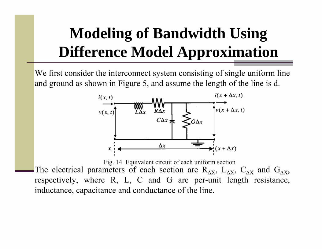
We first consider the interconnect system consisting of single uniform line and ground as shown in Figure 5, and assume the length of the line is d.
The electrical parameters of each section are R∆X, L∆X, C∆X and G∆X, respectively, where R, L, C and G are per-unit length resistance, inductance, capacitance and conductance of the line.
Fig. 14 Equivalent circuit of each uniform section

Using Kirchoff’s Law, we can write
Simplifying the above two equations and applying Laplace transformation, we get
Differentiating equations (3) and (4) with respect to x, and after simplifying we get,
),(),(),(),( txxvdt
txdiLRtxitxv xx ∆+++= ∆∆
),(),(),(),( txxidt
txxdvctxxvGtxi xx ∆++∆+
+∆+= ∆∆
)()()( xIsLRxxV
+=∂
∂−
)()()( xVsCGxxI
+=∂
∂−
)()( 22
2
xVx
xVΡ=
∂∂
)()( 22
2
xIx
xIΡ=
∂∂
(1)
(2)
(3)
(4)
(5)
(6)

The general solution of equation (5) is given by
Where A1 and A2 are the constants determined by the boundary conditions. From equations (5) and (7 )
Assuming at x=d, the termination voltage and current are V (d) =V2 and I (d) =I2, respectively, then we get,
From equation (9) and (10) we get
xx eAeAxV ΡΡ− += 21)( (7)
[ ] )()(21 xIsLReAeAx
xx +=+∂∂
− ΡΡ−
[ ]xx eAeAZ
xI ΡΡ− −= 210
1)((8)
dd eAeAV ΡΡ− += 212
][121
02
dd eAeAZ
I ΡΡ− −=
[ ] deZIVA Ρ+= 0221 21 [ ] deZIVA Ρ−−= 0222 2
1
(9)
(10)
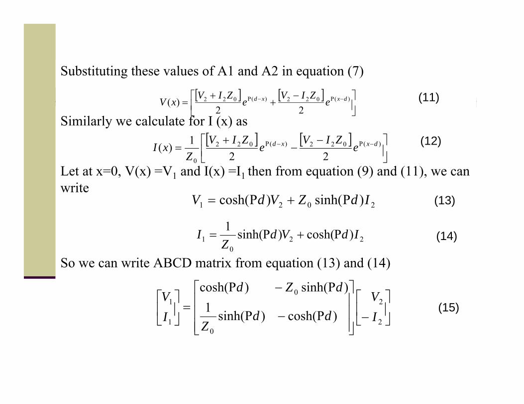
Substituting these values of A1 and A2 in equation (7)
Similarly we calculate for I (x) as
Let at x=0, V(x) =V1 and I(x) =I1 then from equation (9) and (11), we can write
So we can write ABCD matrix from equation (13) and (14)
[ ] [ ]⎥⎦⎤
⎢⎣⎡ −
++
= −Ρ−Ρ )(022)(022
22)( dxxd e
ZIVe
ZIVxV
[ ] [ ]⎥⎦⎤
⎢⎣⎡ −
−+
= −Ρ−Ρ )(022)(022
0 221)( dxxd e
ZIVe
ZIVZ
xI
(11)
(12)
2021 )sinh()cosh( IdZVdV Ρ+Ρ=
220
1 )cosh()sinh(1 IdVdZ
I Ρ+Ρ=
(13)
(14)
⎥⎦
⎤⎢⎣
⎡−
⎥⎥⎥
⎦
⎤
⎢⎢⎢
⎣
⎡
Ρ−Ρ
Ρ−Ρ=⎥
⎦
⎤⎢⎣
⎡
2
2
0
0
1
1
)cosh()sinh(1)sinh()cosh(
IV
ddZ
dZd
IV
(15)

From equation (15), we can write the equation for the transfer function of the system
After simplification, we get from equation (16)
Substitute s=jω in equation (17) and after simplification
Apply modulus on both side and equate to , we get
)cosh(1
)()()(
1
2
dsVsVsH
Ρ== (16)
))((
1)()(
)(1
2
CGs
LRssV
sVsH
++==
(17)
⎟⎠⎞
⎜⎝⎛ ++−
=
CG
LRj
CLRG
jHωω
ω2
1)(
22
22
121
⎟⎠⎞
⎜⎝⎛ ++⎟
⎠⎞
⎜⎝⎛ −
=
CG
LR
CLRG ωω
(18)
(19)
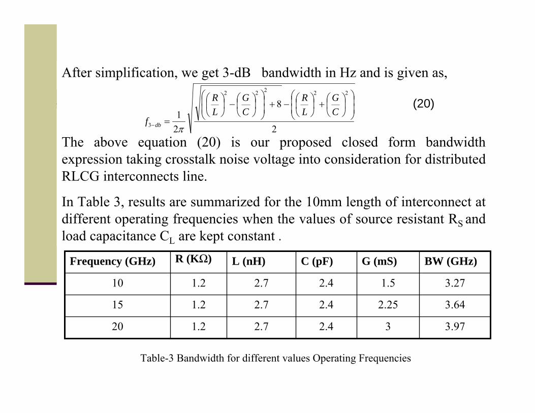
After simplification, we get 3-dB bandwidth in Hz and is given as,
The above equation (20) is our proposed closed form bandwidth expression taking crosstalk noise voltage into consideration for distributed RLCG interconnects line.
In Table 3, results are summarized for the 10mm length of interconnect at different operating frequencies when the values of source resistant RS and load capacitance CL are kept constant .
2
8
21
22222
3
⎟⎟⎠
⎞⎜⎜⎝
⎛⎟⎠⎞
⎜⎝⎛+⎟
⎠⎞
⎜⎝⎛−+⎟
⎟⎠
⎞⎜⎜⎝
⎛⎟⎠⎞
⎜⎝⎛−⎟
⎠⎞
⎜⎝⎛
=−
CG
LR
CG
LR
f db π
(20)
3.9732.42.71.220
3.642.252.42.71.215
3.271.52.42.71.210
BW (GHz)G (mS)C (pF)L (nH)R (KΩ)Frequency (GHz)
Table-3 Bandwidth for different values Operating Frequencies

Conclusion
The first part of the proposed work discussed about an efficient and accurate interconnect delay metric based on Gamma function for high speed VLSI RC global interconnects.In the second part of the proposed work, a brief analytical model is presented for calculating the delay and power for the RLC interconnects.The last part of the work proposed a distributed RLCG transmission line model of interconnects using difference model approach.

Future ProspectsFuture integrated circuits design will be driven by interconnectperformance, not transistor’s performance.New interconnect technologies, such as copper and low-temperature interconnect, may introduce new problems.Alternative solutions such as on-chip optical interconnects have been proposed in order to avoid the problems associated with global on-chip wires altogether.

Publications
Rajib Kar, Vikas Maheshwari, A.K. Mal, A.K. Bhattacharjee, “ Delay Analysis for On-Chip VLSI Interconnect using Gamma Distribution Function”, International Journal of Computer Application (IJCA). Vol. 1, No. 3, Article 11, pp. 77-80, 2010, Foundation of Computer Science (FCA) PressRajib Kar, Vikas Maheshwari, A.K. Mal, A.K. Bhattacharjee, “A Model for Slew Evaluation for On-Chip RC Interconnects using Gamma Distribution Function”, International Journal of Computer Application (IJCA).Vol. 1, No. 10, Article 13, pp. 88-93. 2010, Foundation of Computer Science (FCA) Press.Rajib Kar, Vikas Maheshwari, Md. Maqbool, A.K.Mal, A.K.Bhattacharjee , “ An Explicit Model of Delay and Slew Metric for On-Chip VLSI RC Interconnects for Ramp Inputs using Gamma Distribution Function”, International Journal of Recent Trends in Engineering, Academy Publisher, Finland. Vol. Issue. pp Rajib Kar, Md. Maqbool, Vikas Maheshwari, A.K. Mal, A.K. Bhattacharjee, “Power-Estimation for On-Chip VLSI Distributed RLC Global Interconnect Using Model Order Reduction Technique”, International Journal of Computer Application (IJCA). Vol. 1, No.14. pp. 96-101, 2010. Foundation of Computer Science (FCA) Press

Rajib Kar, Vikas Maheshwari, Md. Maqbool, A.K.Mal, A.K.Bhattacharjee, “A Closed Form Modelling of cross-talk for Distributed RLCG On-Chip Interconnects Using Difference Model Approach”, International Journal on Communication Technology (IJCT), India
Rajib Kar, V. Maheshwari, Md. Maqbool, A.K.Mal, A.K.Bhattacharjee, “An Explicit Coupling Aware Delay Model for Distributed On-Chip RLCG Interconnects Using Difference Model Approach”, International Journal of Embedded Systems and Computer Engineering, Vol. 2 Issue.1.pp.39-42, Serial Publications, India
Rajib Kar, Vikas Maheshwari, Md. Maqbool, Sangeeta Mandal , A.K.Mal, A.K.Bhattacharjee , “Closed Form Bandwidth Expression for Distributed On-Chip RLCG Interconnects”, IEEE International Conference on Advances in Computer Engineering (ACE 2010), pp. June 20-21, 2010 , Bangalore, INDIA
Rajib Kar, V. Maheshwari, Aman Choudhary, Abhishek Singh, Ashis K. Mal, A. K. Bhattacharjee, “Coupling Aware Power Estimation for Distributed On-Chip RLCG Interconnects Using Difference Model Approach”, 2nd IEEE International Conference on Computing, Communication and Networking Technologies (ICCCN 2010), 29th -31st July, 2010 Karur, India.

ReferencesSung-Mo Kang and Yusuf Leblebici,” CMOS Digital Integrated Circuits Analysis and Design”, TMH Publication,2008Intel website, http://www.intel/research/silicon/mooreslaw.htm, Sept. 2010 C. Bermond, B. Flechet, A. Fracy, V. Arnal, J. Torres, G LeCarval, G. Angenieux, and R. Salik. “Impact of Dielectrics and Metals Properties on Electrical Performances of Advanced On-Chip Interconnect,” Proceedings of the International Interconnect Technology Conference, 2002, p. 161-163T. Kikkawa, “Current and Future Low-K Dielectrics for Cu Interconnects,” Proceedings of International Electron Devices Meeting, 2000, p. 253-256.L. Peters, “Pursuing the Perfect Low-K Dielectric,” Semiconductor International, September 1998, p. 64-74. 98 Bibliography C. Cregut, G. Le Carval, J. Chilo. “Low-K Dielectrics Influence on Crosstalk: Electromagnetic Analysis and Characterization,” Proceedings of the International Interconnect Technology Conference, 1998, p. 59-61.R. Donaton, F. Iacopi, M Baklanov, D. Shamiryan, B. Coenegrachts, H. Struyf, M. Lepage, M Meuris, M. Van Hove, W. Gray, H. Meynen, D. DeRoest, S. Vanhaelemeersch, K. Maex, “Physical and Electrical Characterization of Silsesquioxane-Based Ultra-Low k Dielectric Films,” Proceedings of the International Interconnect Technology Conference, 2000, p. 93-95.S. Jang, Y. Chen, T. Chou, S. Lee, C. Chen, T. Tseng, B. Chen, S. Chang, C, Yu, and M. Liang. “Advanced Cu/Low-k (k=2.2) Multilevel Interconnect for 0.10/0.07 mm Generation,” Symposium on VLSI Technology Proceedings, 2002, p. 17-18.M. Anders, N. Rai, R. Krishnamurthy, S. Borkar. “A Transition-Encoded Dynamic Bus Technique for High-Performance Interconnects,” Symposium on VLSI Circuits Proceedings, 2002, p. 16-17.