Combinational Logic Circuits - Clemson Universityyfeaste/855Assignments/presentations... · Adder !...
46
Combinational Logic Circuits CPSC 855 Embedded Systems Fryad M. Rashid and Pei-Lin Chung
Transcript of Combinational Logic Circuits - Clemson Universityyfeaste/855Assignments/presentations... · Adder !...
Combinational Logic Circuits
CPSC 855 Embedded Systems
Fryad M. Rashid and Pei-Lin Chung
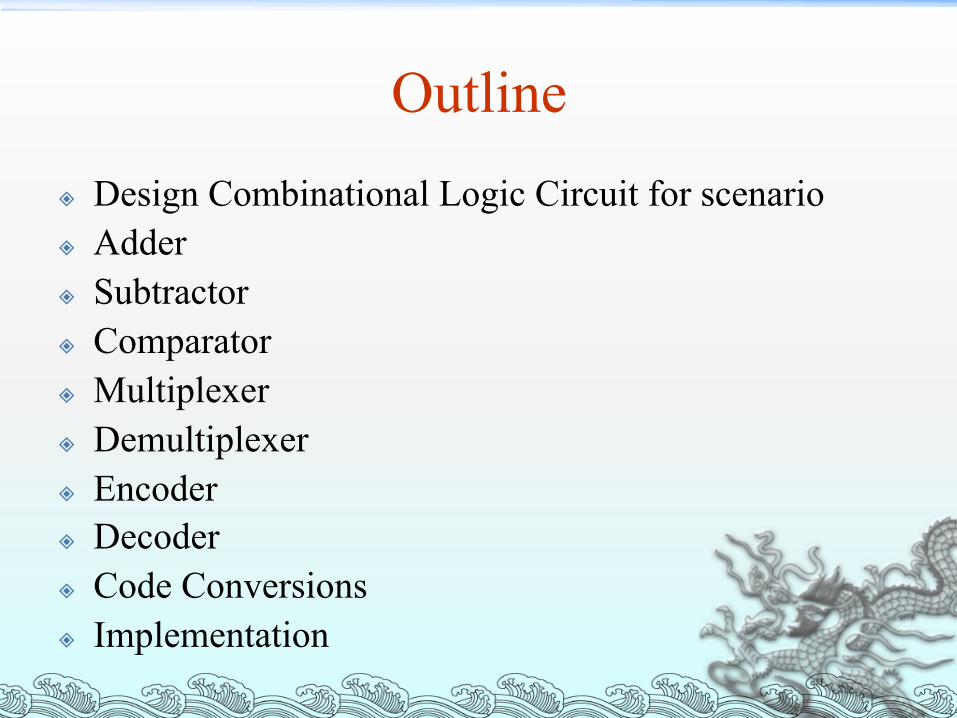
Outline ² Design Combinational Logic Circuit for scenario ² Adder ² Subtractor ² Comparator ² Multiplexer ² Demultiplexer ² Encoder ² Decoder ² Code Conversions ² Implementation
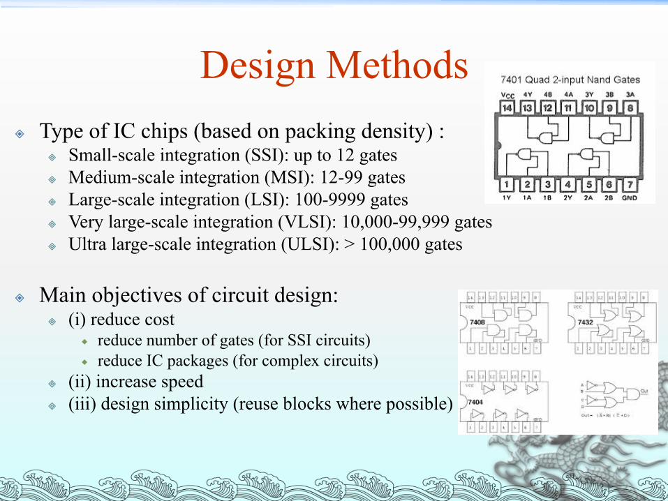
Design Methods ² Type of IC chips (based on packing density) :
³ Small-scale integration (SSI): up to 12 gates ³ Medium-scale integration (MSI): 12-99 gates ³ Large-scale integration (LSI): 100-9999 gates ³ Very large-scale integration (VLSI): 10,000-99,999 gates ³ Ultra large-scale integration (ULSI): > 100,000 gates
² Main objectives of circuit design: ³ (i) reduce cost
® reduce number of gates (for SSI circuits) ® reduce IC packages (for complex circuits)
³ (ii) increase speed ³ (iii) design simplicity (reuse blocks where possible)
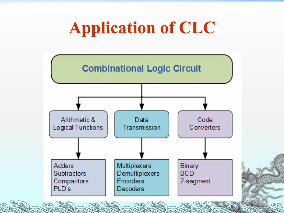
Application of CLC

Introduction
Combinational Logic Circuits (Circuits without a memory): In this type of logic circuits outputs depend only on the current inputs.
Sequential Logic Circuits (Circuits with memory): In this type of logic circuits outputs depend on the current inputs and previous inputs. These circuits employ storage elements and logic gates.

Combinational Logic Circuits
² A combinational circuit consists of input variables (n), logic gates, and output variables (m).
² For (n) input variables there are 2n possible combinations of binary input values.
² For each possible input combination there is one and only one possible output combination, a combinational circuit can be describe by (m) Boolean functions one for each output variable.
² Each output function expressed in terms of the (n) input variables.
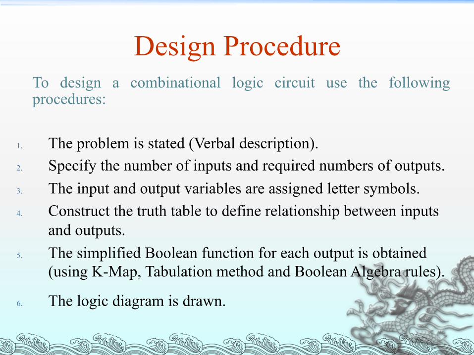
Design Procedure
1. The problem is stated (Verbal description). 2. Specify the number of inputs and required numbers of outputs. 3. The input and output variables are assigned letter symbols. 4. Construct the truth table to define relationship between inputs
and outputs. 5. The simplified Boolean function for each output is obtained
(using K-Map, Tabulation method and Boolean Algebra rules).
6. The logic diagram is drawn.
To design a combinational logic circuit use the following procedures:

Practical Design
A practical design method would have to consider such constrains as: 1. Min. no. of gates. 2. Min. no. of inputs to gates. 3. Min. no. of interconnections. 4. Min. propagation time of the signal throw the circuit.

Simple Design – Remind You Example: Simplify two inputs OR gate truth table by using K-Map? 1.Problem is stated. 2.No. of inputs are two (X and Y) & No. of required output is (F) 3.Construct truth table (F= X+Y), inputs =2 è 22=4 possibilities 4.Using K-Map to simplify the circuit. 5.Final design.

Design for scenario
² A committee of three individuals decide issues for an organization. Each individual votes either yes or no for each proposal that arises. A proposal is passed if it receives at least two yes votes. Design a circuit that determines whether a proposal passes.

Solution Inputs are three (x, y, z) , Output is proposal (F)
We used truth table to make a relationship between inputs and output.
We used K-Map minimization technique to simplify the circuit.

Adders
² Digital computers perform a variety of information processing tasks. Among the basic functions encountered are the various arithmetic operations (addition).

Binary Adder -Half Adder Q/Design a combinational logic circuit that performs arithmetic
operation for adding two bits? Answer: n=2 bit , n=22=4
0 + 0 = 0 0 + 1 = 1 1 + 0 = 1 1 + 1 = 10

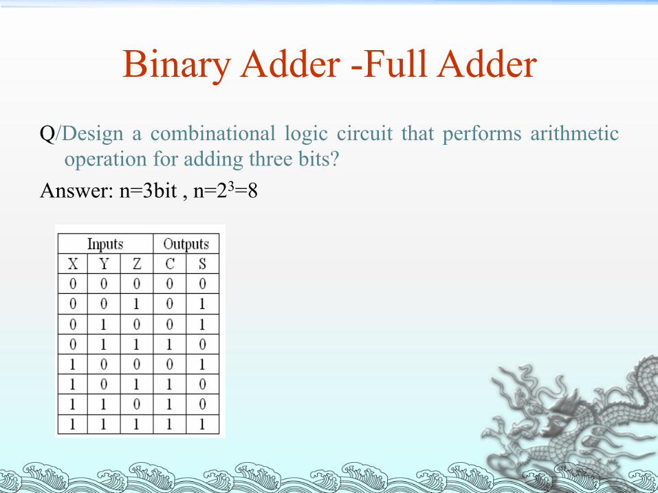
Binary Adder -Full Adder Q/Design a combinational logic circuit that performs arithmetic
operation for adding three bits? Answer: n=3bit , n=23=8

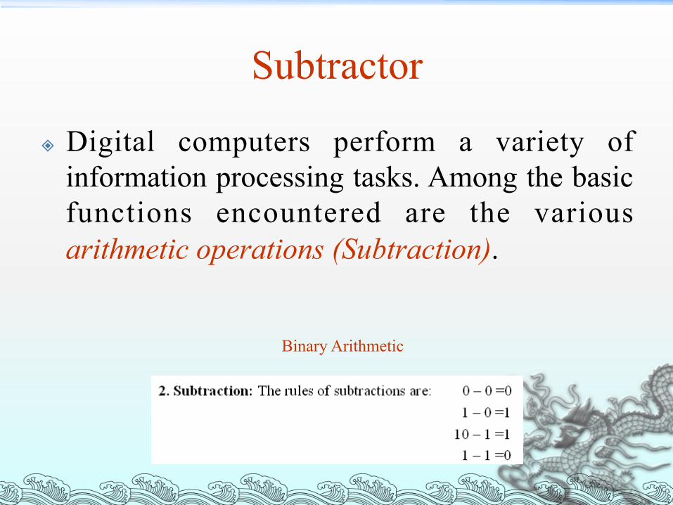
Subtractor
² Digital computers perform a variety of information processing tasks. Among the basic functions encountered are the various arithmetic operations (Subtraction).
Binary Arithmetic
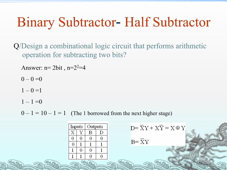
Binary Subtractor- Half Subtractor Q/Design a combinational logic circuit that performs arithmetic
operation for subtracting two bits?
Answer: n= 2bit , n=22=4
0 – 0 =0
1 – 0 =1
1 – 1 =0
0 – 1 = 10 – 1 = 1 (The 1 borrowed from the next higher stage)

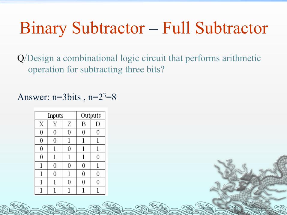
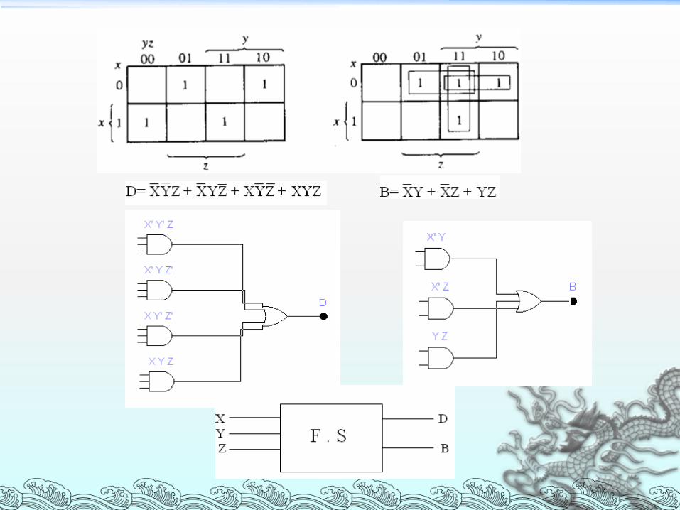
Binary Subtractor – Full Subtractor Q/Design a combinational logic circuit that performs arithmetic
operation for subtracting three bits? Answer: n=3bits , n=23=8
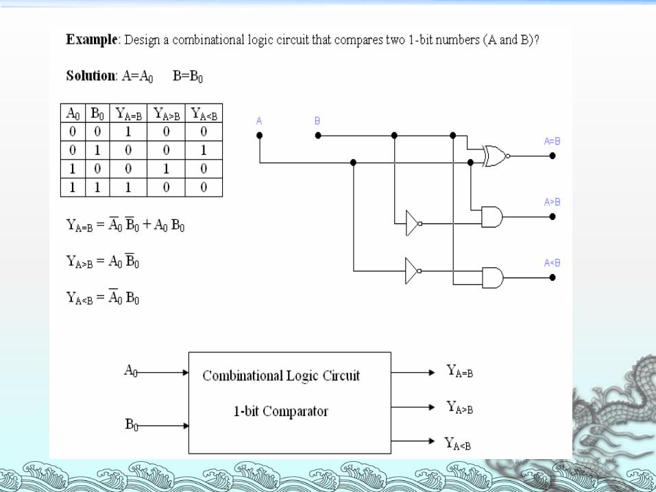
Comparator
The comparison of two numbers is an operation that determines if one number is greater than, less than, or equal to the other number. A comparator is a CLC that compares two numbers A, B, and determines their relative magnitudes. The outcome of the comparison is specified my three binary variables that indicate whether A>B, A=B, or A<B.

Multiplexer (Data Selector)
Design MUX:
AND gates used to represent inputs.
One OR gate only used to collect inputs.
NOT gates as a selector to connect inputs to output.
Multiplexing means transmitting a large number of information units over a smaller number of channels or lines. A digital multiplexer is CLC that selects binary information from one of many input lines and directs it to a single output line. The selection of a particular input line is controlled by of a selection lines.
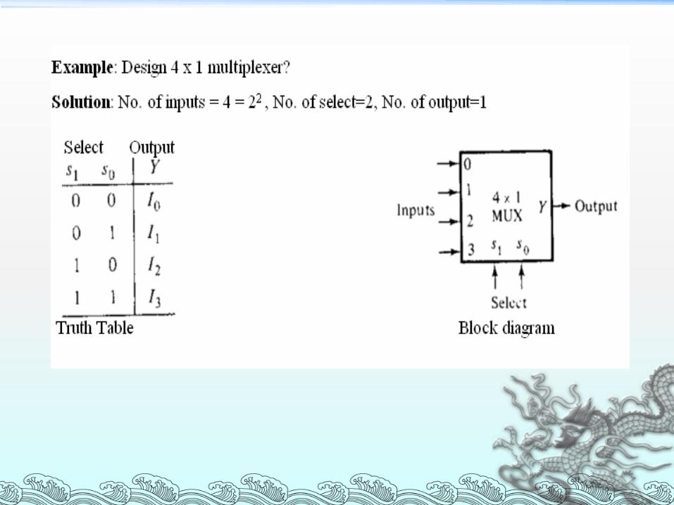

4x1 Multiplexer Logic Diagram
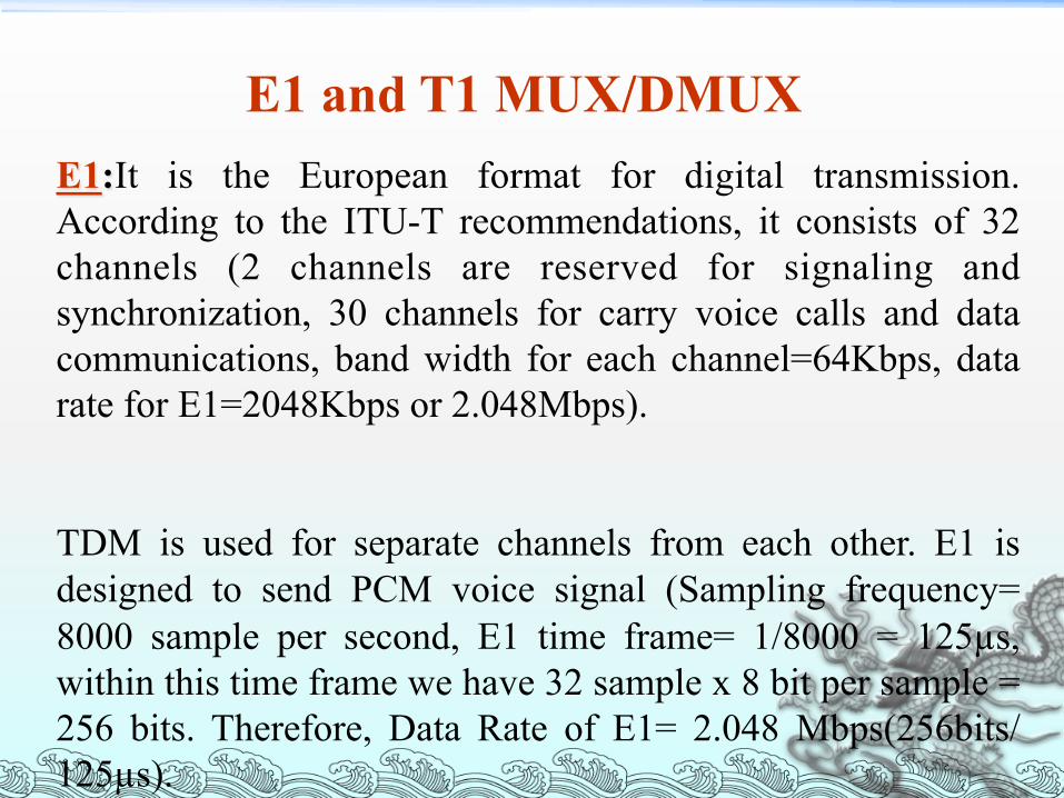
E1:It is the European format for digital transmission. According to the ITU-T recommendations, it consists of 32 channels (2 channels are reserved for signaling and synchronization, 30 channels for carry voice calls and data communications, band width for each channel=64Kbps, data rate for E1=2048Kbps or 2.048Mbps).
TDM is used for separate channels from each other. E1 is designed to send PCM voice signal (Sampling frequency= 8000 sample per second, E1 time frame= 1/8000 = 125µs, within this time frame we have 32 sample x 8 bit per sample = 256 bits. Therefore, Data Rate of E1= 2.048 Mbps(256bits/125µs).
E1 and T1 MUX/DMUX
E1 and T1 MUX/DMUX
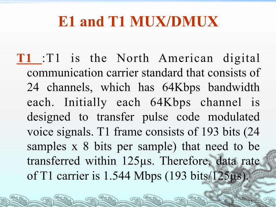
T1 :T1 is the North American digital communication carrier standard that consists of 24 channels, which has 64Kbps bandwidth each. Initially each 64Kbps channel is designed to transfer pulse code modulated voice signals. T1 frame consists of 193 bits (24 samples x 8 bits per sample) that need to be transferred within 125µs. Therefore, data rate of T1 carrier is 1.544 Mbps (193 bits/125µs).

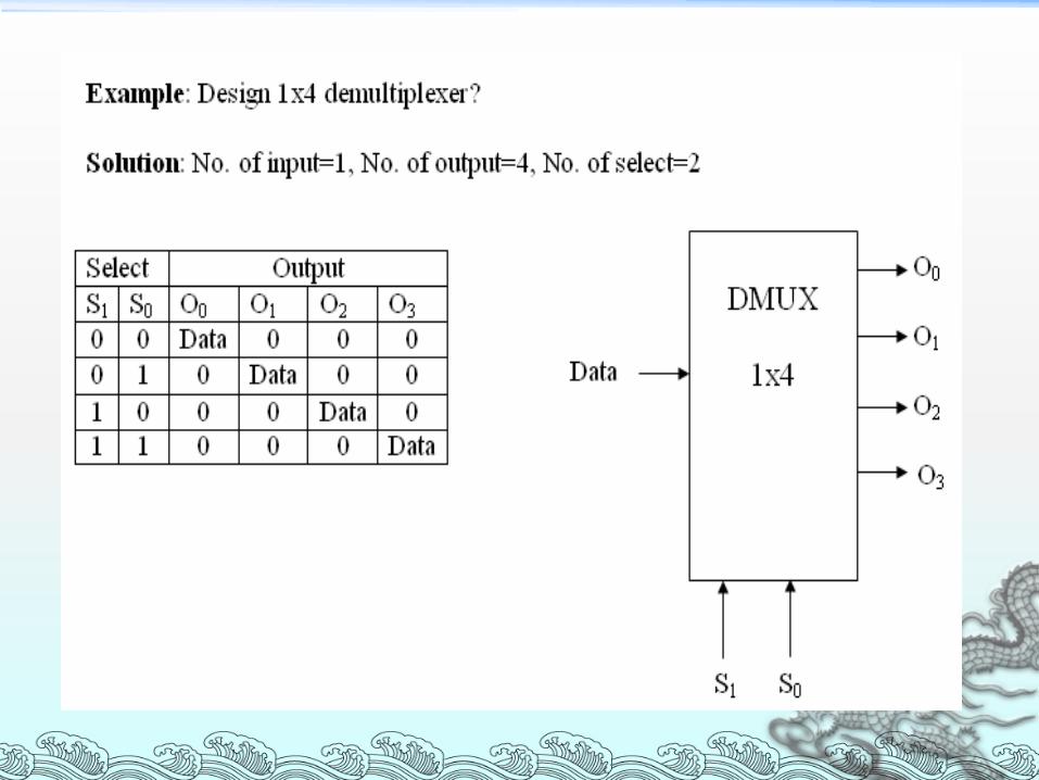
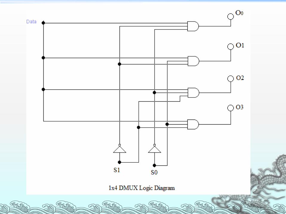
Demultiplexer
Design DMUX:
AND gates used to represent inputs.
NOT gates as a selector to connect inputs to output.
A demultiplexer performs the reverse operation of a multiplexer i.e. it receives one input and distributes it over several outputs.
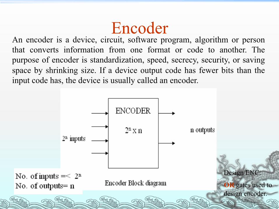
Encoder
Design ENC:
OR gates used to design encoder.
An encoder is a device, circuit, software program, algorithm or person that converts information from one format or code to another. The purpose of encoder is standardization, speed, secrecy, security, or saving space by shrinking size. If a device output code has fewer bits than the input code has, the device is usually called an encoder.


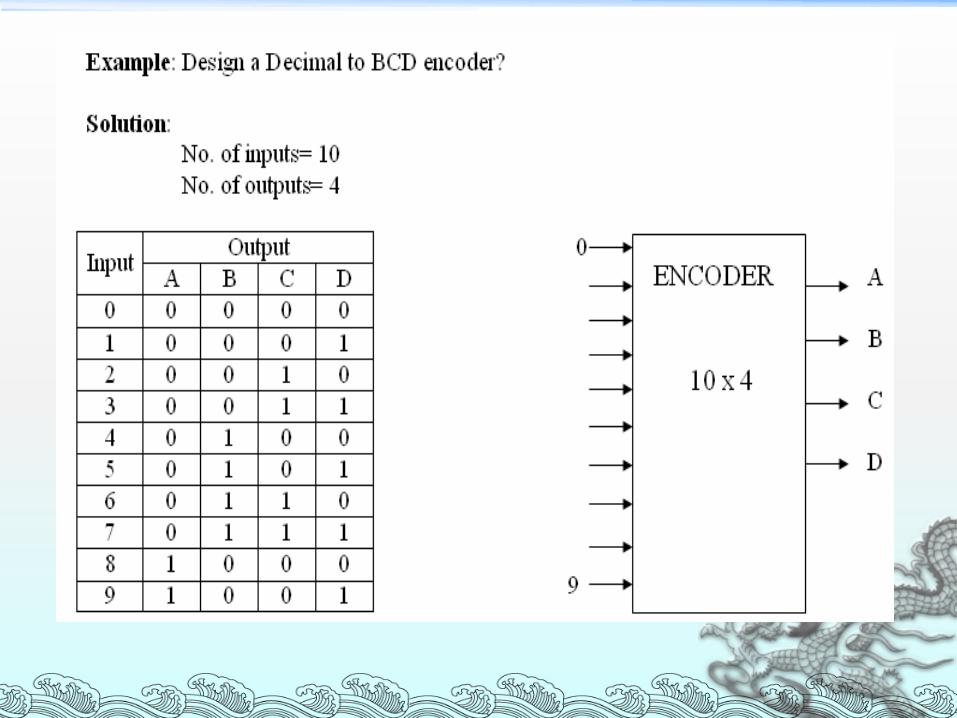

Decimal to BCD Encoder logical diagram

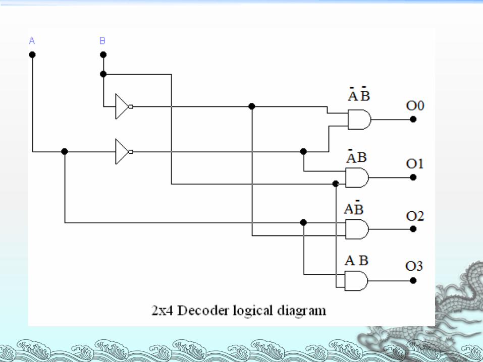
Decoder A decoder is a combinational circuit that converts binary information from n input lines to a maximum of 2n unique output lines.
Design DEC:
AND gates used to represent inputs.
NOT gates to connect inputs to output.


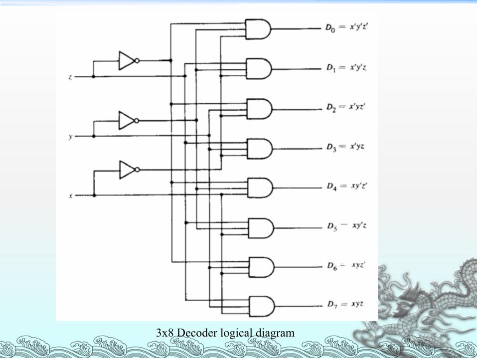
3x8 Decoder logical diagram
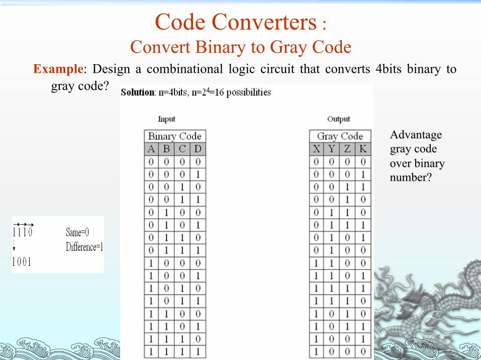
Code Converters : Convert Binary to Gray Code
Example: Design a combinational logic circuit that converts 4bits binary to gray code?
Advantage gray code over binary number?


4bit binary to gray code converter

Implementation
² Electronics Workbench Circuit Board Design and Simulation Software such as EWB, Multisim, ..etc

References
² http://www.tutorialspoint.com/computer_logical_organization/combinational_circuits.htm
² http://www.differencebetween.com/difference-‐between-‐e1-‐and-‐vs-‐t1/
² http://coep.vlab.co.in/?sub=28&brch=81&sim=609&cnt=1