CHAPTER The Silicon-on-Sapphire Fabrication … simplicity and reduction of fabrication masks needed...
38
CHAPTER 1 The Silicon-on-Sapphire Fabrication Process 1.1 Introduction Silicon-on-insulator technology (SOI) is one of the available technolo- gies to fabricate integrated circuits. Traditional circuit manufacturing technologies employ a conductive and doped silicon wafer, and, for this reason, are often referred as “bulk complementary metal–oxide semiconductor (CMOS) processes.” Bulk CMOS devices and circuits are manufactured on the silicon surface. SOI technologies use a silicon–insulator–silicon substrate in place of bulk substrates. This kind of substrate allows to reduce the parasitic capacitances for each device and therefore provide improvements in performance. This chapter discusses a type of SOI called silicon-on-sapphire (SOS), describing its fabrication process, its advantages, and the basic devices available. The objective of this chapter is to familiarize the reader with the SOI/SOS fabrication process, starting from the phys- ical constraint of fabrication, moving to device characterization, and, finally, introducing the design of SOI/SOS circuits and systems. SOI fabrication processes are discussed in Sec. 1.3 of this chapter. The SOS wafer is introduced in Sec. 1.4, while its fabrication process is described in Sec. 1.5. Section 1.6 presents an overview of SOS metal- oxide-semiconductor field effect transistors (MOSFETs) and their ad- vantages. Section 1.7 discusses in detail SOS MOSFETs in strong and weak inversion and offers preliminary statistical data from an en- semble of different dies. Section 1.7 ends with a useful comparison between data and simulation of SOS MOSFETs. 1
Transcript of CHAPTER The Silicon-on-Sapphire Fabrication … simplicity and reduction of fabrication masks needed...

July 8, 2009 14:4 Culurciello/Silicon-on-Sapphire Circuits and Systems/Eugenio Culurciello /160848-6/Ch01
C H A P T E R 1The Silicon-on-Sapphire
Fabrication Process
1.1 IntroductionSilicon-on-insulator technology (SOI) is one of the available technolo-gies to fabricate integrated circuits. Traditional circuit manufacturingtechnologies employ a conductive and doped silicon wafer, and, forthis reason, are often referred as “bulk complementary metal–oxidesemiconductor (CMOS) processes.” Bulk CMOS devices and circuitsare manufactured on the silicon surface.
SOI technologies use a silicon–insulator–silicon substrate in placeof bulk substrates. This kind of substrate allows to reduce the parasiticcapacitances for each device and therefore provide improvements inperformance.
This chapter discusses a type of SOI called silicon-on-sapphire(SOS), describing its fabrication process, its advantages, and the basicdevices available. The objective of this chapter is to familiarize thereader with the SOI/SOS fabrication process, starting from the phys-ical constraint of fabrication, moving to device characterization, and,finally, introducing the design of SOI/SOS circuits and systems.
SOI fabrication processes are discussed in Sec. 1.3 of this chapter.The SOS wafer is introduced in Sec. 1.4, while its fabrication processis described in Sec. 1.5. Section 1.6 presents an overview of SOS metal-oxide-semiconductor field effect transistors (MOSFETs) and their ad-vantages. Section 1.7 discusses in detail SOS MOSFETs in strong andweak inversion and offers preliminary statistical data from an en-semble of different dies. Section 1.7 ends with a useful comparisonbetween data and simulation of SOS MOSFETs.
1
July 8, 2009 14:4 Culurciello/Silicon-on-Sapphire Circuits and Systems/Eugenio Culurciello /160848-6/Ch01
2 C h a p t e r O n e
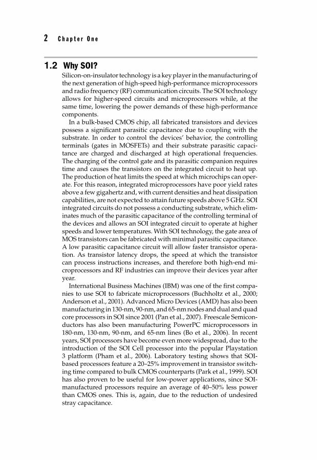
1.2 Why SOI?Silicon-on-insulator technology is a key player in the manufacturing ofthe next generation of high-speed high-performance microprocessorsand radio frequency (RF) communication circuits. The SOI technologyallows for higher-speed circuits and microprocessors while, at thesame time, lowering the power demands of these high-performancecomponents.
In a bulk-based CMOS chip, all fabricated transistors and devicespossess a significant parasitic capacitance due to coupling with thesubstrate. In order to control the devices’ behavior, the controllingterminals (gates in MOSFETs) and their substrate parasitic capaci-tance are charged and discharged at high operational frequencies.The charging of the control gate and its parasitic companion requirestime and causes the transistors on the integrated circuit to heat up.The production of heat limits the speed at which microchips can oper-ate. For this reason, integrated microprocessors have poor yield ratesabove a few gigahertz and, with current densities and heat dissipationcapabilities, are not expected to attain future speeds above 5 GHz. SOIintegrated circuits do not possess a conducting substrate, which elim-inates much of the parasitic capacitance of the controlling terminal ofthe devices and allows an SOI integrated circuit to operate at higherspeeds and lower temperatures. With SOI technology, the gate area ofMOS transistors can be fabricated with minimal parasitic capacitance.A low parasitic capacitance circuit will allow faster transistor opera-tion. As transistor latency drops, the speed at which the transistorcan process instructions increases, and therefore both high-end mi-croprocessors and RF industries can improve their devices year afteryear.
International Business Machines (IBM) was one of the first compa-nies to use SOI to fabricate microprocessors (Buchholtz et al., 2000;Anderson et al., 2001). Advanced Micro Devices (AMD) has also beenmanufacturing in 130-nm, 90-nm, and 65-nm nodes and dual and quadcore processors in SOI since 2001 (Pan et al., 2007). Freescale Semicon-ductors has also been manufacturing PowerPC microprocessors in180-nm, 130-nm, 90-nm, and 65-nm lines (Bo et al., 2006). In recentyears, SOI processors have become even more widespread, due to theintroduction of the SOI Cell processor into the popular Playstation3 platform (Pham et al., 2006). Laboratory testing shows that SOI-based processors feature a 20–25% improvement in transistor switch-ing time compared to bulk CMOS counterparts (Park et al., 1999). SOIhas also proven to be useful for low-power applications, since SOI-manufactured processors require an average of 40–50% less powerthan CMOS ones. This is, again, due to the reduction of undesiredstray capacitance.

July 8, 2009 14:4 Culurciello/Silicon-on-Sapphire Circuits and Systems/Eugenio Culurciello /160848-6/Ch01
T h e S i l i c o n - o n - S a p p h i r e F a b r i c a t i o n P r o c e s s 3
Another key benefit of SOI is a reduction in soft error rates (SER).Soft errors refer to data corruption caused by cosmic rays and naturalradioactive background signals. SER will be an important issue asmicroprocessors scale to smaller die sizes and lower voltages. SOIchips demonstrate a significant reduction in SER-related issues, evenfor integrated circuits with a large die area (such as microprocessors).
At the same time, SOI and SOS analog circuits can benefit from theinsulating substrate and provide higher performance at lower powerdraw. In this and the next few chapters of this book, we focus on the ad-vantages of SOS technology for analog and mixed-signal microsystemdesign. The next generation of mobile-targeted circuits and systemswill demand a combination of high-performance digital and analogcircuits. This book, by providing a fresh perspective on these new tech-nologies, seeks to offer a fundamental contribution to the successfuldevelopment of SOI and SOS circuits.
1.3 The SOS Fabrication ProcessSilicon-on-insulator is a very-large-scale integration (VLSI) fabricationprocess in which a thin layer of silicon is deposited on the top of aninsulating material (Kuo and Su, 1998). SOS, in which the insulatingmaterial is synthetic sapphire, was one of the first SOI processes avail-able. In an SOI process, active metal–oxide–semiconductor (MOS) de-vices and other passive devices are fabricated in and on the thin layerof silicon.
In SOS, a thin layer of silicon is grown on top of a sapphire substrate,as can be seen in the bottom portion of Fig. 1.1. In this figure, the maindifference between bulk CMOS, SOS, and SOI are clearly visible. At thetop of Fig. 1.1 we show the cross-section of a typical deep-submicronCMOS process. In this cross-section the example circuit is a CMOSinverter. Notice the large number of layers needed to design NMOSand PMOS devices and the need of wells to insulate them from eachother and from the conductive substrate. Also notice the requiredcontacts to the well to keep them in reverse bias with respect to thesubstrate and reduce parasitic conduction. On the other hand the SOSprocess cross-section, presented in Fig. 1.1, shows a clear advantagein simplicity and reduction of fabrication masks needed to designthe same CMOS inverter circuit. SOS MOSFETs are obtained on aultrathin (100 nm) film of silicon grown on top of a sapphire substrate.The sapphire substrate itself is grown artificially. The bottom cross-section of Fig. 1.1 shows the same CMOS inverter implemented in anSOI process. SOI uses a buried silicon dioxide layer to separate thetop thin film of silicon and obtain similar benefits and reductions inmanufacturing steps that SOS provides.

July 8, 2009 14:4 Culurciello/Silicon-on-Sapphire Circuits and Systems/Eugenio Culurciello /160848-6/Ch01
4 C h a p t e r O n e
P+ substrate
P epitaxial layer
P wellN well
N+ N+ N+
Bulk CMOS Process
Insulating sapphire substrate
Peregrine SOS Process
Isolation
Isolation
Polysilicon gate MetalN-well contact
P-channel FET N-channel FET
Insulating Sapphire Substrate
SOI Process
Isolation
P-channel FET N-channel FET
P+ substrate
SiO2 oxide layer
P+ P+ P+
FIGURE 1.1 Comparison of the CMOS wafer cross-section (top), an SOSCMOS wafer (middle), and an SOI CMOS wafer (bottom). The circuit ineach of these cross-sections is a CMOS inverter (Peregrine, 2008a).
Historically, the SOS process has been utilized and developed for itsproperty of radiation tolerance (or radiation hardness), the ability towithstand environments with high radiation (Cristoloveanu and Li,1995). The thin film of silicon is not thick enough to interact with ion-izing radiation, and therefore the system is less susceptible than othersystems to single-event charged particles upsets. In addition, the insu-lating layer or substrate shields the thin film devices from radiation-generated hole–electron pairs. In a bulk process, the effect of radiationis severe in the operation of active MOS devices, because the carriers

July 8, 2009 14:4 Culurciello/Silicon-on-Sapphire Circuits and Systems/Eugenio Culurciello /160848-6/Ch01
T h e S i l i c o n - o n - S a p p h i r e F a b r i c a t i o n P r o c e s s 5
generated in the bulk substrate by ionizing radiation can significantlyaffect the device characteristics and, moreover, induce latch-up or evenpermanent damage. The insulating substrate in SOI/SOS eliminatesworrisome latch-up conditions. Because there is no substrate, the par-asitic bipolar junction transistors (BJTs) are not present, and thereforethe problem of latch-up does not arise.
Because of their property of radiation tolerance, SOI and SOS arevery popular in military and space applications. Until recently, how-ever, the low yield in the fabrication of VLSI circuits using these pro-cesses have prevented them from being successful in the commercialmarket, restricting them to corner niches in the space and military sec-tors, where yield and cost are not an issue because of the low numbersof components needed.
1.3.1 Advantages of SOSFrom a design point of view, the main advantage of SOI/SOS is theinsulation between MOS active devices and the substrate. This insu-lation frees the devices from the parasitic capacitances in connectionto the substrate, increasing the quality factor of passive componentsand the performance of active MOS devices. The lack of these para-sitics to the substrate implies a lack of stray capacitances. Smaller par-asitic capacitances reduce the burden on devices and allow transistorsto operate faster, as their capacitive load is reduced. Circuit instabilitiesdue to undesired capacitive feedback are also significantly reduced. Inthe case of MOSFET devices, the feedback capacitance between inputand output is due only to the gate capacitance in SOI/SOS.
The substrate isolation gives SOI/SOS a density advantage duringfabrication. SOI/SOS devices can be spaced more closely than bulkprocesses, since the latter need to reverse bias PN junctions to isolateportions of the circuits. This is evident in Fig. 1.1, where a cross-sectionof a typical bulk process is compared with a SOS process. The circuit inthe figure is a CMOS inverter. A typical example of bulk reverse biasedisolation is the N-well in a P substrate. The spacing between activeregions and wells severely limits density in bulk complementary MOS(CMOS).
Recently, SOI processes have been more and more widely adopted,especially since IBM started manufacturing microprocessors in SOI[PowerPC model 750, year 1999 and 2000 (Buchholtz et al., 2000)].Such commercial success has been encouraged by the recent develop-ment of a commercially available foundry of SOS CMOS technologyby Peregrine Semiconductor Corp. of San Diego, CA (Peregrine, 2003).Peregrine is a leading supplier of high-speed mixed-signal integratedcircuits (ICs) for wireless and fiber-optic communications. Peregrine’sproduct family is based on its patented ultrathin silicon (UTSi) CMOS

July 8, 2009 14:4 Culurciello/Silicon-on-Sapphire Circuits and Systems/Eugenio Culurciello /160848-6/Ch01
6 C h a p t e r O n e
wafer fabrication process. A cross-section of a CMOS inverter in thisprocess is given in Fig. 1.1. UTSi ICs have substantial advantages—lower cost, lower power consumption, higher levels of integration,and superior RF performance-in comparison to ICs that are fabricatedin competing high-performance mixed-signal processes. Peregrineproducts include RF MOS switches, high-performance phase-lockedloops (PLL), MOSFET mixers, monolithic digital step attenuators,RF prescalers, line drivers and receivers, and frequency synthesizers(Stuber et al., 1998; Megahed et al., 1998).
1.3.2 Disadvantages of SOSOne disadvantage of the SOS process is the lower heat conductiv-ity of the sapphire substrate—typically one-half the conductivity ofsilicon. Also, a monolith crystal wafer of sapphire is about twice asexpensive to fabricate as a silicon wafer. However, the number of fab-rication masks is reduced in SOS, because of the absence of some of thebulk CMOS process layers, such as wells, trenches, and other isolationstructures.
The cost of developing SOS circuits is constantly decreasing as thenumber of clients increases and demand rises. With recent trends andincreasing demand for low-power low-voltage circuits, SOS currentlyis and will continue to play an important role in the future of VLSI,as will become apparent in the sections on device characteristics andcircuits that follow.
1.4 SOS Wafer ManufacturingThe development of a high-yield SOS process requires many techno-logical advances, some of which are described in this section and inFig. 1.2. Much of SOS technology was developed in the 1970s, whenthe process became popular. Sapphire was chosen as a substrate el-ement because of its relative availability and its silicon-compatibleproperties, in particular its thermal mismatch and its crystallographicparameters (Cristoloveanu and Li, 1995).
An SOS wafer is prepared by cutting a single crystal sapphire(Al3O2) approximately 60◦ to the c axis (Kuo and Su, 1998). The sap-phire crystal is typically obtained using Czockralsky growth and edge-defined film-fed growth. The sapphire surface has to be carefully fin-ished with subsequent steps of polishing and annealing before it canreceive the silicon film.
The sapphire substrate is carefully polished and cleaned ultrasoni-cally before being inserted in the growth apparatus. The single crystalsapphire is placed in a chemical vapor deposition (CVD) chamber,

July 8, 2009 14:4 Culurciello/Silicon-on-Sapphire Circuits and Systems/Eugenio Culurciello /160848-6/Ch01
T h e S i l i c o n - o n - S a p p h i r e F a b r i c a t i o n P r o c e s s 7
Al2O3
Si
(1) (2)
Si+
(3)
FIGURE 1.2 Fabrication of an SOS wafer: (1) CVD deposition of thin film ofsilicon on the sapphire substrate at about 900◦C, (2) ion implantation of Si+for amorphization at 300◦C, (3) anneal and CVD deposition of silicon at900◦C.
flushed with hydrogen, and heated to 1000–1200◦C using an RF gen-erator. When thermal equilibrium is reached, the chamber is filledwith silane (SiH4) and silicon deposition begins.
Initially, only small hemispherical silicon islands grow on the sap-phire substrate. These islands gradually enlarge until a thin film ofabout 20 nm is formed. Due to the crystallographic mismatch of sap-phire and silicon, this thin film grows with a high-defect density.Aluminum deposits are also a source of contamination before coa-lescence, and therefore this initial growth has to occur at high rate(2 �m/min). Subsequent growth is slower to reduce the defect den-sity. When the desired silicon film thickness has been reached, thesilane flow is stopped. The thickness of the deposited silicon layer inthe Peregrine SOS process is 100 nm.
The wafers are then slowly cooled in hydrogen to anneal and crys-tallize the surface. The most damaging step is the postgrowth cool-ing phase, when differential contraction occurs and causes strongcompression of the silicon film. Silicon thermal expansion is 3.8 ×10⁻⁸/◦C−1, whereas, it is 9.2 × 10⁻⁸/◦C−1 for sapphire (Al3O2).
In the past, low yield has been due to the poor quality of interface be-tween the silicon and the sapphire. Imperfection due to the interfacematching of the crystalline structures causes failure lines in the de-posited silicon. Peregrine Semiconductors recently developed (1990)a technique to obtain almost perfect silicon in sapphire interfaces,thus bringing the yield of circuits to production acceptable levels.The purity of the SOS interface in Peregrine wafers can be seen inFig. 1.3. In this figure, the Peregrine wafer is compared to a conven-tional SOS wafer, where the density of defects is higher (Reedy, 1982);

July 8, 2009 14:4 Culurciello/Silicon-on-Sapphire Circuits and Systems/Eugenio Culurciello /160848-6/Ch01
8 C h a p t e r O n e
FIGURE 1.3 Micrograph of an unoptimized SOS wafer (left) and PeregrineSOS wafer (right) defects at the silicon–sapphire interface. Notice thatPeregrine wafer’s defect density is lower than conventional SOS wafer’sdefect density (?).
(Garcia et al., 1988). The reason is that the sapphire crystal usedby Peregrine is rhombohedral and therefore different from the face-centered cubic silicon crystal (Cristoloveanu and Li, 1995). The defectdensity in a conventional SOS process can reach values as high as 1 Mplanar faults/cm and 109 line defects/cm2.
A recently developed technique that reduces defect density is calledsolid phase epitaxy (SPE). In SPE, silicon ions are implanted in the thinsilicon film to render it amorphous. The implant of silicon ions on thesapphire surface has to occur at very low energies to minimize damageto the substrate. The implant resets the damaged interface; followinga 900◦C anneal, the bottom silicon layer is crystallized once again. SPEand CVD can occur at the same time to finely control the thickness ofthe silicon layer (Reedy et al., 1983).
The use of SPE technique substantially reduces the defect densityby acting on the compression strain, by suppressing the transitionlayer, and by reducing the density of microtwins, stacking faults, andinterface traps. The surface can be enhanced with a subsequent siliconimplant and epitaxial regrowth.
The electrical characteristics of the SOS wafer are greatly influencedby the fabrication process. In particular, lateral stress, the silicon–sapphire transition layer, and deep inhomogeneities play a dramaticrole in altering the silicon energy bands. The twisting of the valenceand conduction bands because of fabrication stresses give SOS pe-culiar transport characteristics. In the case of (100) SOS wafers, thecompression stress causes the kx and ky ellipsoids to become morepopulated with electrons than the kz ellipsoid (which is normal to thesilicon surface). Other effects on mobility are due to surface scatter-ing when the doping profiles are high. In addition, self-heating is a

July 8, 2009 14:4 Culurciello/Silicon-on-Sapphire Circuits and Systems/Eugenio Culurciello /160848-6/Ch01
T h e S i l i c o n - o n - S a p p h i r e F a b r i c a t i o n P r o c e s s 9
Process NMOS mobility [cm2/V s] PMOS mobility [cm2/V s]
HP 0.5 �m 431.50 145.38
AMI 0.5 �m 467.79 152.85
SOS 0.5 �m 230.00 134.43
TABLE 1.1 Table of extracted low-field mobility of P and N MOSFETs inthree 0.5-�m processes offered by MOSIS (MOSIS, 1999)
common problem of SOS and SOI devices, due to the lower thermalconductivity of the substrates and thus the removal of excess heat. Asa result, the effective mass of the electron increases and decreases forholes. The effects visible in the devices include increased hole mobi-lity and reduced drift mobility for electrons (up to 25% as reported inCristoloveanu and Li, 1995).
Table 1.1 offers an example of the different properties of SOS tech-nology, reporting a comparison of low-field mobility of P and NMOSFETs in three 0.5-�m processes offered by MOSIS (MOSIS, 1999).
In Table 1.1, the NMOS values of low-field mobility are almost halfof the values obtained in comparable bulk CMOS process with thesame feature size of 0.5 �m.
1.5 Peregrine SOS Process FeaturesPeregrine offers several SOS processes (see Peregrine, 2003) with a va-riety of configuration. Some processes are optimized for digital logic,some offer RF quality passives, some are optimized for radiation-hard environments, and some for GHz operation and fast RF circuits.Throughout this book, we have used the Peregrine process namedwith code FC. The FC process has a single poly layer and three metallayers. The FC process’s main advantage is that its third metal layer(metal-3 or metal-thick) is a thick metal layer (3 �m thick). All metallayers are made of aluminum. Metal insulator metal (MIM) capaci-tors are available between the second metal layer (metal-2) and thetop metal layer. This allows the production of very-high-quality factor(Q) passive components such as capacitors and inductors. Capacitorsand inductors have a high-quality factor because the effect of para-sitic capacitance is very limited. Inductors made in the top metal-thicklayer have low series resistance and, therefore, high-quality factor (Q).Resistors also benefits from the insulating substrate because the dis-tributed parasitic capacitance is eliminated. In bulk CMOS processes,large resistors have very-low-quality factors and reduce bandwidthdue to the distributed capacitance to the substrate.

July 8, 2009 14:4 Culurciello/Silicon-on-Sapphire Circuits and Systems/Eugenio Culurciello /160848-6/Ch01
10 C h a p t e r O n e
The FC process’s nominal operating voltage is 3.3 V, and the maxi-mum allowed voltage is 3.6 V.
1.5.1 Local IsolationIsolation of SOS devices is obtained with a technique usually referredas LOCOS (local isolation of silicon). Figure 1.1 shows a cross-sectionof a NMOS and PMOS in close vicinity. Between the two devices, thesilicon thin film is etched away and a thick field oxide is grown tokeep the transistors isolated.
The isolation is obtained with a dual-step LOCOS isolation(Cristoloveanu and Li, 1995). The first step consists of masking theactive region of the silicon thin film with silicon nitride. Then fieldoxide is grown in the field region, and then etched away to producethese rounded active regions (Fig. 1.1). The silicon between the activeregions is then removed with reactive ion etching (RIE) all the wayto the sapphire substrate. A second local oxide deposition is then ap-plied so that the isolation field oxide has the same thickness of thesilicon thin film. The result is the LOCOS isolation in Fig. 1.1. Thistechniques reduces bird’s beak and silicon filaments under the activeregion. These undesired effects lower the isolation of devices becauseof encroachment near the sapphire.
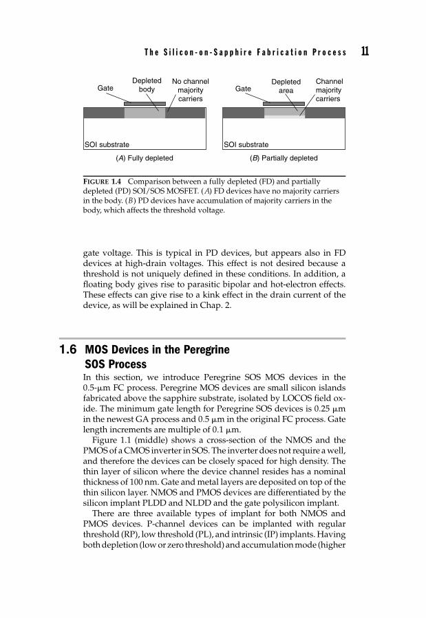
1.5.2 Fully Depleted DevicesIn the Peregrine SOS, because of the thickness of the silicon thin film(100 nm), the depletion region under the gate reaches the sapphiresubstrate when the gate is at a zero potential. The devices obtainedin this kind of silicon thin film are usually referred as fully depleted(FD). FD devices thus have a body that is completely void of majoritycarriers. This is in contrast to partially depleted (PD) devices, where asmall layer of majority carriers is present in the body when the gate isbiased at a zero potential. Figure 1.4 shows the difference between fullydepleted and partially depleted MOSFET devices. Majority carriers inFD devices are absorbed by the source and drain regions.
Fully depleted devices have several advantages over partially de-pleted devices (Cristoloveanu and Li, 1995). First, the transconduc-tance of the devices is higher because of the better gate control overthe silicon thin film. Since the device is already fully depleted withthe gate at zero potential, any increase of the gate voltage will induceconduction in the channel. In a PD device, the gate voltage first hasto remove the excess majority carrier in the body before contributingto form a channel. Second, fully depleted devices do not suffer fromfloating body effect.
One adverse effect of the accumulation of majority carriers in thedevice body is that the threshold voltage becomes a function of the
July 8, 2009 14:4 Culurciello/Silicon-on-Sapphire Circuits and Systems/Eugenio Culurciello /160848-6/Ch01
T h e S i l i c o n - o n - S a p p h i r e F a b r i c a t i o n P r o c e s s 11
Depletedbody
SOI substrate
GateNo channel
majoritycarriers
(A) Fully depleted
Depletedarea
SOI substrate
GateChannelmajoritycarriers
(B) Partially depleted
FIGURE 1.4 Comparison between a fully depleted (FD) and partiallydepleted (PD) SOI/SOS MOSFET. (A) FD devices have no majority carriersin the body. (B) PD devices have accumulation of majority carriers in thebody, which affects the threshold voltage.
gate voltage. This is typical in PD devices, but appears also in FDdevices at high-drain voltages. This effect is not desired because athreshold is not uniquely defined in these conditions. In addition, afloating body gives rise to parasitic bipolar and hot-electron effects.These effects can give rise to a kink effect in the drain current of thedevice, as will be explained in Chap. 2.
1.6 MOS Devices in the PeregrineSOS ProcessIn this section, we introduce Peregrine SOS MOS devices in the0.5-�m FC process. Peregrine MOS devices are small silicon islandsfabricated above the sapphire substrate, isolated by LOCOS field ox-ide. The minimum gate length for Peregrine SOS devices is 0.25 �min the newest GA process and 0.5 �m in the original FC process. Gatelength increments are multiple of 0.1 �m.
Figure 1.1 (middle) shows a cross-section of the NMOS and thePMOS of a CMOS inverter in SOS. The inverter does not require a well,and therefore the devices can be closely spaced for high density. Thethin layer of silicon where the device channel resides has a nominalthickness of 100 nm. Gate and metal layers are deposited on top of thethin silicon layer. NMOS and PMOS devices are differentiated by thesilicon implant PLDD and NLDD and the gate polysilicon implant.
There are three available types of implant for both NMOS andPMOS devices. P-channel devices can be implanted with regularthreshold (RP), low threshold (PL), and intrinsic (IP) implants. Havingboth depletion (low or zero threshold) and accumulation mode (higher
July 8, 2009 14:4 Culurciello/Silicon-on-Sapphire Circuits and Systems/Eugenio Culurciello /160848-6/Ch01
12 C h a p t e r O n e
MOS Description MOS Type VT (V) Application
RN Regular Vt N-channel 0.65 Digital, low-leakage
NL Low Vt N-channel 0.14 High-perform. digital, RF
IN Intrinsic Vt N-channel −0.2 High-perform. digital, RF
RP Regular Vt P-channel −0.6 Digital, low-leakage
PL Low Vt P-channel −0.25 High-perform. digital, RF
IP Intrinsic Vt P-channel −0.03 High-perform. digital, RF
TABLE 1.2 Summary table of Peregrine SOS transistors types,threshold voltages, and typical applications.
threshold) is one of the advantages of the isolation properties of thesilicon on sapphire technology. In bulk CMOS, accumulation devicescannot be obtained without separate wells because of the lack of iso-lation in the commonly shared substrate.
N-channel devices can be implanted with regular threshold (RN),low threshold (NL), and intrinsic (IN) implants. Regular-thresholddevices are the accumulation devices typical of bulk CMOS; theirthreshold voltage is targeted to about 0.7 V. Low-threshold devicesare accumulation devices with a voltage threshold of about 0.3 V. In-trinsic devices are depletion MOS devices, with a voltage threshold ofabout 0 V. The minimum-size intrinsic devices can produce �A levelcurrents with no bias voltage. A summary of the transistor types, theirthresholds, and their typical usage is given in Table 1.2.
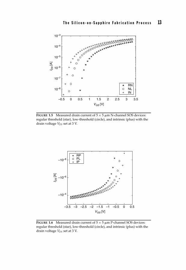
For digital applications, the main tradeoff between transistor typesis the magnitude of leakage drain current with the gate voltage set tozero versus the switching speed. Another tradeoff is low-voltage oper-ation versus switching speed, especially for lower-threshold devices.Figures 1.5 and 1.6 show measured transistor characteristics for thedifferent N-channel and P-channel transistors, respectively. Lookingat Fig. 1.5 for N-channel devices, it is evident that at zero-gate voltage,regular threshold devices offer only leakage subthreshold currents onthe order of less than 1 pA. At zero-gate voltage, low-threshold de-vices offer tenths of �A of subthreshold current, while an intrinsicdevice gives hundreds of �A, since the transistor is turned on andthe drain current is substantial. The same kind of behavior is visiblein Fig. 1.6, but the leakage levels of the P-channel devices are lowerthan the N-channel ones because of the difference in doping implants.For analog application, the different threshold can be used for a largevariety of circuit topologies. Low-threshold transistors allow stack-ing of devices at low operational voltages. Intrinsic devices can act as
July 8, 2009 14:4 Culurciello/Silicon-on-Sapphire Circuits and Systems/Eugenio Culurciello /160848-6/Ch01
T h e S i l i c o n - o n - S a p p h i r e F a b r i c a t i o n P r o c e s s 13
0–0.5 0.5 1 1.5 2 2.5 3 3.5
10–8
10–7
10–6
10–5
10–4
10–3
VGS [V]
I DS [A
]
RNNLIN
FIGURE 1.5 Measured drain current of 5 × 5 �m N-channel SOS devices:regular threshold (star), low-threshold (circle), and intrinsic (plus) with thedrain voltage VDS set at 3 V.
0.50–0.5–1–1.5–2–2.5–3–3.5
–10–8
–10–6
–10–4
VGS [V]
I DS [A
]
RPPLIP
FIGURE 1.6 Measured drain current of 5 × 5 �m P-channel SOS devices:regular threshold (star), low-threshold (circle), and intrinsic (plus) with thedrain voltage VDS set at 3 V.

July 8, 2009 14:4 Culurciello/Silicon-on-Sapphire Circuits and Systems/Eugenio Culurciello /160848-6/Ch01
14 C h a p t e r O n e
unbiased current sources or can operate at very low supply voltages.A few examples of circuit topologies using Peregrine SOS transistorswill be given throughout the entire book and in the chapters thatfollow.
In summary, the negative impact of lower-threshold voltage tran-sistors is a higher standby current for CMOS application. The benefitsof lower-threshold transistors include:
• Improved transition frequency ( ft) due to increased carrier mo-bility as a result of lower channel doping
• Improved digital switching speed, especially at lower powersupply voltages
• Low or zero headroom reduction across transistors
• Reduced kink effect in the N-channel transistors, since the lowerthreshold transistors have depleted bodies
The kink effect degrades the device characteristics for analog ap-plications; it will be discussed in Chap. 2. Lower-threshold transistorsare recommended for high-speed, RF, and analog applications. RNand RP transistors are recommended for digital logic and low-leakageapplications.
Compared to bulk CMOS devices, SOS MOSFETs have the advan-tage of much reduced body effect, and lower short and narrow channeleffects (Colinge, 1997). The back-gate effect in SOS devices is virtuallyzero, so no modulation of the threshold is due to the substrate bias.A short-channel effect can change the threshold voltage by up to fourtimes in bulk CMOS, but less than 50% in SOS devices. Drain-inducedbarrier lowering, or DIBL, is also lower in SOS MOSFETs as comparedto bulk CMOS devices. All these effects are an important feature ofSOS and SOI devices. A larger current drive capability can be obtainedwhen body effects are removed, giving SOS devices an additional ad-vantage in speed when compared to bulk CMOS MOSFETs.
1.7 SOS MOS Characteristicsfor Analog DesignDevice characteristics are a very important starting point for state-of-the-art analog design in SOS. Such characteristics can be used toevaluate the best operating region for each transistor in the circuit,and to assess the constant (DC) current levels at each voltage set-ting. The characteristics also give visual insight to high-order differ-ential parameters, such as the small signal models and the device gain.

July 8, 2009 14:4 Culurciello/Silicon-on-Sapphire Circuits and Systems/Eugenio Culurciello /160848-6/Ch01
T h e S i l i c o n - o n - S a p p h i r e F a b r i c a t i o n P r o c e s s 15
We provide here a set of device characteristics collected from SOS MOSdevices of various types. We measured above- and below-thresholdcharacteristics, as well as transconductance parameters. Additionalcharacteristics include device current leakage and matching data.
1.7.1 Transistor Transconductance ParameterThe transconductance of a MOS transistor quantifies the drain currentvariation with a gate-source voltage variation while keeping the drain-source voltage constant. This is an important parameter for the designof analog circuits because it defines a gain profile for each device. Inaddition, the MOS transistor is a natural transconductor because ofthe dependence of the input gate voltage on the output drain current.The MOS intrinsic transconductance gm is defined in Eq. (1.1), whereVGS and VDS are the DC bias voltages.
gm =[
∂iDS
∂vGS
]VGS,VDS=const
(1.1)
A first-order model for the hand calculation of gm can be obtainedin the three regions of operation: subthreshold, ohmic, and saturation.Each model approximates the transconductance in each region of op-eration, reducing the complexity of the formulation. Equations (1.2)and (1.3) are the simplified analytical form of gm, respectively, in theohmic region and in the saturation region. These equations are derivedfrom Eq. (1.1) and the drain current relation in each operating region.
gm = �0COXWL
VDS (1.2)
gm = �0COXWL
(VGS − Vth) (1.3)
In Eqs. (1.2) and (1.3), Vth is the gate voltage threshold, �0 is thecarrier mobility, and COX is the gate capacitance. In weak inversion,MOS transconductance is given by Eq. (1.4).
gm = IDk
VT(1.4)
where VT is the thermal voltage, k is the MOS gate capacitance (COX)divided by itself plus the substrate or device body (Cdep), as fromEq. (1.5).
k = COX
COX + Cdep(1.5)

July 8, 2009 14:4 Culurciello/Silicon-on-Sapphire Circuits and Systems/Eugenio Culurciello /160848-6/Ch01
16 C h a p t e r O n e
Normalized transconductance is given by the ratio of gm and the draincurrent (gm/ID). In the subthreshold, the normalized transconduc-tance is given by Eq. (1.6).
gm
ID= k
VT(1.6)
Normalizing the transconductance makes it clear to determinewhich region of the MOSFET offers the maximum gain as a propor-tion of the drain current. This is particularly useful for low-powerdesign, where it is important to both reduce the drain current and max-imize the transconductance gain. The normalized transconductanceof a MOS reaches its maximum value in the subthreshold region ofweak inversion, where the MOS shows an exponential relationship be-tween gate voltage and drain current. In weak inversion, the MOSFETthe normalized transconductance reaches the theoretical limit of a BJTdevice, or a transconductance of 1/VT (gm = k/VT ).
The maximum theoretical normalized transconductance in the MOStransistor equals the BJT case if k equals 1. In this case, the normalizedtransconductance maximum is just above 40 [V−1] at room temper-ature. Note that, by measuring the transistor’s normalized transcon-ductance with precision, it is possible to estimate the MOS transistor’sk parameter.
Equations (1.2) and (1.4) can be used for above-threshold design ofa first-order circuit topology, but they fail to help in the low-voltageregion of weak inversion. Also, they do not take into account short-and narrow-channel effects and channel nonuniformities.
A set of measured data of SOS MOSFETs can help the designeridentify operational region and the expected current gain of the de-vice. We measured SOS MOSFET DC characteristics and computed thetransconductance. We measured the relationship between the draincurrent and the gate voltage of the device. We computed the transcon-ductance gm by numerical methods on the MOS raw characteristics. Inorder to precisely compute first-order derivative of the MOS charac-teristics these have to be measured accurately. The measurements ofthe drain current were taken with increments of gate voltage of 1 mVand with a drain voltage VDS of 3 V. This allows numerical methodsof integration to have the required computational precision withoutoverestimating the transconductance values. This data was smoothedwith a running average filter to reduce noise.
Figure 1.7 is a plot of the normalized transconductance of a set of RNSOS MOS transistors. The device sizes were (width, length): 1.2 × 0.8,2.5 × 2.5, 25 × 5, and 25 × 10 �m. Figures 1.9 and 1.11 are a plot ofthe normalized transconductance of a set of, respectively, NL and INSOS MOS transistors. The device sizes were (width, length): 1.2 × 0.5,2.5 × 2.5, 25 × 5, and 25 × 10 �m. Equivalently, Figs. 1.8, 1.10, and 1.12are plots of the normalized transconductance of a set of P-channel SOSMOS transistors, respectively, RP, PL, and IP. The device sizes were

July 8, 2009 14:4 Culurciello/Silicon-on-Sapphire Circuits and Systems/Eugenio Culurciello /160848-6/Ch01
T h e S i l i c o n - o n - S a p p h i r e F a b r i c a t i o n P r o c e s s 17
0 0.2 0.4 0.6 0.8 1
0
5
10
15
20
25
30
35
VGS [V]
g m/I D
[1/V
]
RN1.2 × 0.8RN2.5 × 2.5RN25 × 5RN25 × 10
FIGURE 1.7 Measured transconductance parameters for a set of SOS RNMOSFETs. The legend correlates different curves to transistor sizes. Thedrain voltage is set at 3 V.
(width, length): 1.2 × 0.5, 2.5 × 2.5, 25 × 5, and 25 × 10 �m. The RNMOSFETs in Fig. 1.7 show a peak normalized transconductance at agate voltage of 0.2–0.4 V. The RP MOSFETs in Fig. 1.8 show a peaknormalized transconductance at a gate voltage of 0.2–0.4 V. The NL
0–0.2–0.4–0.6–0.8–1
5
10
15
20
25
VGS [V]
g m/I D
[1/V
]
RP1.2 × 0.5RP2.5 × 2.5RP25 × 5RP25 × 10
FIGURE 1.8 Measured transconductance parameters for a set of SOS RPMOSFETs. The legend correlates different curves to transistor sizes. Thedrain voltage is set at 3 V.

July 8, 2009 14:4 Culurciello/Silicon-on-Sapphire Circuits and Systems/Eugenio Culurciello /160848-6/Ch01
18 C h a p t e r O n e
0–0.2–0.4 0.2 0.4 0.6 0.80
5
10
15
20
25
30
VGS [V]
g m/I D
[1/V
]
NL1.2 × 0.5NL25 × 0.5NL25 × 5NL25 × 10
FIGURE 1.9 Measured transconductance parameters for a set of SOS NLMOSFETs. The legend correlates different curves to transistor sizes. Thedrain voltage is set at 3 V.
MOSFETs in Fig. 1.9 show a peak normalized transconductance at agate voltage of 0 V. The PL MOSFETs in Fig. 1.10 show a peak normal-ized transconductance at a gate voltage of 0 V. The IN MOSFETs inFig. 1.11 show a peak normalized transconductance at a gate voltage
0.4–0.245–0.890
5
10
15
20
25
30
VGS [V]
g m/I D
[1/V
]
PL1.2 × 0.5PL2.5 × 2.5PL25 × 5PL25 × 10
FIGURE 1.10 Measured transconductance parameters for a set of SOS PLMOSFETs. The legend correlates different curves to transistor sizes. Thedrain voltage is set at 3 V.

July 8, 2009 14:4 Culurciello/Silicon-on-Sapphire Circuits and Systems/Eugenio Culurciello /160848-6/Ch01
T h e S i l i c o n - o n - S a p p h i r e F a b r i c a t i o n P r o c e s s 19
0 0.5–0.5–10
5
10
15
20
25
30
35
40
VGS [V]
g m/I D
[1/V
]
IN1.2 × 0.5IN2.5 × 2.5IN25 × 5IN25 × 10
FIGURE 1.11 Measured transconductance parameters for a set of SOS INMOSFETs. The legend correlates different curves to transistor sizes. Thedrain voltage is set at 3 V.
of −0.6 V. The IP MOSFETs in Fig. 1.12 show a peak normalizedtransconductance at a gate voltage of −0.2 V.
Notice that the normalized transconductance data presented here isnot flat in the subthreshold region as suggested by the theory and, in
0–0.2–0.4–0.6–0.8
0
5
10
15
20
25
VGS [V]
g m/I D
[1/V
]
IP1.2 × 0.5IP2.5 × 2.5IP25 × 5IP25 × 10
FIGURE 1.12 Measured transconductance parameters for a set of SOS IPMOSFETs. The legend correlates different curves to transistor sizes. Thedrain voltage is set at 3 V.

July 8, 2009 14:4 Culurciello/Silicon-on-Sapphire Circuits and Systems/Eugenio Culurciello /160848-6/Ch01
20 C h a p t e r O n e
particular, Eq. (1.6). Besides, the limitation of the leakage currentsof each device, which reduce the normalized transconductance tozero at very-low gate voltages, the subthreshold current become pro-gressively higher than their derivative, resulting in a decrease of thenormalized transconductance at low gate voltages. The normalizedtransconductance data presented here are from multiple devices indifferent dies, so some mismatch in the response needs to be accountedfor. These curve nevertheless provide substantial insight on which de-vices can be used for specific applications. One final comment is thatin Figs. 1.9 and 1.11, the shorter-length devices result in much lowertransconductances than larger-length devices. This is due to the short-channel effect and is expected. Intrinsic and low-threshold transistorsalso have larger leakage current, so their normalized transconduc-tance is reduced.
1.7.2 Modeling the Subthreshold RegionFor the design of low-power low-voltage circuits, the subthresholdcharacteristics of the MOS devices is of great importance and interest.This is because the low current produced by the device in a weak inver-sion keeps the circuit operating with limited supply current and very-low power consumption. The supply voltage can also be reduced,since the drain currents are small, and this allows the entire circuitto run on an even more stringent power budget. In addition, the ex-ponential characteristic of the subthreshold regime in a MOS is verydesirable in many linear applications (Sinencio and Andreou, 1998).Trade-offs and advantages of subthreshold operation of SOS MOS willbe discussed in this and the following chapters.
Like conventional bulk MOS transistors, SOS MOSFETs exhibitdrain currents that, below threshold, are an exponential function of thegate voltage for a given DC voltage sweep. There are various devicephysical models to describe this relationship, but we chose to modelthe drain current with Eq. (1.7).
ID = WL
I0ekVGS
VT e(1−k)VBS
VT (1.7)
W and L are the width and length of the active region of the tran-sistor, VGS refers to the gate-source voltage (equal to the potential ofthe gate since the source is tied to the ground potential), and VT is thethermal voltage, equal to kT/q . Since the bulk terminal is not presentin SOS MOSFETs, the VBS voltage can be thought as the voltage be-tween the device’s body and the source of the device (assume that itis connected to the ground voltage reference). In SOS, the body of thedevice is a floating one. If the device is fully depleted, the body voltagewill not be influenced by the other terminals and the dependance on

July 8, 2009 14:4 Culurciello/Silicon-on-Sapphire Circuits and Systems/Eugenio Culurciello /160848-6/Ch01
T h e S i l i c o n - o n - S a p p h i r e F a b r i c a t i o n P r o c e s s 21
VBS can be included in the base current term I0. Therefore, Eq. (1.8)is used to quantify the exponential behavior only as a function of thegate voltage.
ID = WL
I0ekVGS
VT (1.8)
Using Eq. (1.8), we have extracted the parameters I0 and k for eachof the different transistor types and for all transistor sizes. These pa-rameters were obtained fitting the data collected on a variety of MOStransistors with different sizes and for N- and P-channel devices. Thedrain voltage was kept at 3 V and the gate voltage was varied. Thedevice sizes were (width, length): 1.2 × 0.8 (N-channel), 1.2 × 0.5(P-channel), 2.5 × 2.5, 25 × 0.8 (N-channel), 25 × 0.5 (the P-channel),25 × 5, and 25 × 10 �m. The resulting optimized extracted data isgiven in Table 1.3 for N-channel devices and in Table 1.4 for P-channel
Estimated Optimized
Transistor In0 Kn In0 Kn
RN 25 × 10 1.0000E-15 9.9000E-01 8.3206E-16 9.9390E-01
RN 2.5 × 2.5 1.7000E-14 8.2000E-01 1.7178E-14 8.1884E-01
RN 1.2 × 0.8 3.0000E-12 7.0000E-01 4.5128E-12 6.6688E-01
RN 25 × 0.8 3.0000E-15 1.3000E+00 4.3345E-15 1.2704E+00
RN 25 × 5 2.0000E-14 9.9000E-01 4.3735E-14 9.3998E-01
NL 1.2 × 0.5 1.0500E-06 1.3000E-01 1.0611E-06 1.3076E-01
NL 25 × 0.5 9.8000E-07 1.7000E-01 1.0317E-06 1.6274E-01
NL 2.5 × 2.5 6.1000E-08 3.7000E-01 5.6224E-08 3.6635E-01
NL 25 × 10 6.4000E-09 7.9000E-01 6.6946E-09 7.1629E-01
NL 25 × 5 5.0000E-09 3.7000E-01 4.6304E-09 7.7419E-01
IN 2.5 × 2.5 5.3000E-04 5.5000E-01 5.7891E-04 5.5900E-01
IN 1.2 × 0.5 7.9000E-06 1.0500E-01 7.9352E-06 1.0606E-01
IN 25 × 0.5 Erratic Data Erratic Data Erratic Data Erratic Data
IN 25 × 5 1.0500E-04 5.6000E-01 1.5119E-04 5.7836E-01
IN 25 × 10 3.4500E-05 5.8000E-01 3.0982E-05 5.7500E-01
TABLE 1.3 Table of estimated and optimized parameters of theexponential model for SOS subthreshold region of an N-channel device.

July 8, 2009 14:4 Culurciello/Silicon-on-Sapphire Circuits and Systems/Eugenio Culurciello /160848-6/Ch01
22 C h a p t e r O n e
Estimated Optimized
Transistor Ip0 Kp Ip0 Kp
RP 2.5 × 2.5 5.8000E-14 −8.0000E-01 7.4495E-14 −7.8301E-01
RP 1.2 × 0.5 1.2000E-13 −8.7000E-01 8.1470E-14 −9.4876E-01
RP 25 × 0.5 1.6000E-10 −5.0000E-01 1.7456E-10 −5.1002E-01
RP 25 × 5 2.0000E-14 7.0000E-01 3.8419E-14 −6.7009E-01
RP 25 × 10 3.0000E-14 −6.1000E-01 2.3773E-14 −6.3195E-01
PL 2.5 × 2.5 2.5000E-10 −8.7000E-01 2.5353E-10 −9.0032E-01
PL 25 × 0.5 8.9000E-08 −4.2000E-01 9.2562E-08 −4.0084E-01
PL 25 × 10 8.8000E-11 −7.8000E-01 6.8887E-11 −8.2088E-01
PL 25 × 5 1.5000E-10 −7.5000E-01 1.5954E-10 −7.7758E-01
PL 1.2 × 0.5 2.5000E-10 −8.7000E-01 2.4350E-10 −8.8315E-01
IP 2.5 × 2.5 3.3000E-08 7.7000E-01 4.2455E-08 −8.0336E-01
IP 1.2 × 0.5 3.5000E-07 −6.5000E-01 4.2641E-07 −6.7694E-01
IP 25 × 0.5 Erratic Data Erratic Data Erratic Data Erratic Data
IP 25 × 5 2.8000E-08 −7.7000E-01 1.8893E-08 −7.3508E-01
IP 25 × 10 5.5000E-08 −7.8000E-01 4.8059E-08 −7.4945E-01
TABLE 1.4 Table of estimated and optimized parameters of theexponential model for SOS subthreshold region of a P-channel device.
devices. Estimated values are the input to the error minimization func-tion and optimized values are the resulting final values. Once the correctinterval bounds were chosen, the optimized parameter values werein almost all cases very close to the estimated values. Note that twotransistors, the IN and IP 25 × 0.5 �m, returned nonreliable erraticdata and will have to be reexamined in future data collection.
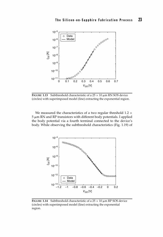
To conclude the collection of subthreshold parameters, we presentin the following figures some examples of plots using optimizedparameter values for all six types of transistors with dimensionsW = 25 �m, L = 10 �m. The drain voltage was kept at 3 V and thegate voltage was varied. The figures represent data in circles and theextracted exponential model superimposed to validate it. Figure 1.13shows an RN device, Fig. 1.14 shows an RP device, Fig. 1.15 shows anNL device, Fig. 1.16 shows PL device, Fig. 1.17 shows an IN device,and Fig. 1.18 shows an IP device.
Both regular-threshold N and P devices offer an exponential regimewith a dynamic range of four decades, from approximately 10−11 to10−7A.
July 8, 2009 14:4 Culurciello/Silicon-on-Sapphire Circuits and Systems/Eugenio Culurciello /160848-6/Ch01
T h e S i l i c o n - o n - S a p p h i r e F a b r i c a t i o n P r o c e s s 23
0 0.1 0.2 0.3 0.4 0.5 0.6 0.710–11
10–10
10–9
10–8
10–7
10–6
10–5
VGS [V]
I DS [A
]
DataModel
FIGURE 1.13 Subthreshold characteristic of a 25 × 10 �m RN SOS device(circles) with superimposed model (line) extracting the exponential region.
We measured the characteristics of a two regular threshold 1.2 ×5 �m RN and RP transistors with different body potentials. I appliedthe body potential via a fourth terminal connected to the device’sbody. While observing the subthreshold characteristics (Fig. 1.19) of
0–0.4 –0.2–0.6–0.8–1–1.2 0.210–14
10–12
10–10
10–8
10–6
10–4
VGS [V]
I DS [A
]
DataModel
FIGURE 1.14 Subthreshold characteristic of a 25 × 10 �m RP SOS device(circles) with superimposed model (line) extracting the exponentialregion.

July 8, 2009 14:4 Culurciello/Silicon-on-Sapphire Circuits and Systems/Eugenio Culurciello /160848-6/Ch01
24 C h a p t e r O n e
0–0.1–0.2–0.3–0.4–0.5 0.1 0.210–12
10–10
10–8
10–6
10–4
VGS [V]
I DS [A
]
DataModel
FIGURE 1.15 Subthreshold characteristic of a 25 × 10 �m NL SOS device(circles) with superimposed model (line) extracting the exponential region.
the regular threshold NMOS device biased with drain voltage VDS setat 3 V, we noticed a significant difference in the behavior of the devicewith bulk floating or at the potential of the source with respect to thecase of VBS lower than the source voltage. The curves for VBS floating orzero were significantly different from the curves for VBS = −0.5 or −1.
0–0.2–0.4–0.6 0.2 0.410–12
10–10
10–8
10–6
10–4
VGS [V]
I DS [A
]
DataModel
FIGURE 1.16 Subthreshold characteristic of a 25 × 10 �m PL SOS device(circles) with superimposed model (line) extracting the exponential region.

July 8, 2009 14:4 Culurciello/Silicon-on-Sapphire Circuits and Systems/Eugenio Culurciello /160848-6/Ch01
T h e S i l i c o n - o n - S a p p h i r e F a b r i c a t i o n P r o c e s s 25
DataModel
0–0.2–0.4–0.6–0.8–110–14
10–12
10–10
10–8
10–6
10–4
VGS [V]
I DS [A
]
FIGURE 1.17 Subthreshold characteristic of a 25 × 10 �m IN SOS device(circles) with superimposed model (line) extracting the exponential region.
We can explain this phenomenon by recognizing that the device is notfully depleted when the bulk is left floating or no negative voltageis applied. Therefore, the NMOS presents nonzero charge in the bulkregion, which lowers the subthreshold slope k. In fact, from Eq. (1.5),
DataModel
0–0.2–0.4 0.2 0.4 0.610–14
10–12
10–10
10–8
10–6
10–4
VGS [V]
I DS [A
]
FIGURE 1.18 Subthreshold characteristic of a 25 × 10 �m IP SOS device(circles) with superimposed model (line) extracting the exponential region.

July 8, 2009 14:4 Culurciello/Silicon-on-Sapphire Circuits and Systems/Eugenio Culurciello /160848-6/Ch01
26 C h a p t e r O n e
0 0.2 0.4 0.6 0.810–14
10–12
10–10
10–8
10–6
VGS [V]
I DS [A
]
VBS 1 VVBS 0.5 VVBS 0 VNo Bulk
FIGURE 1.19 Subthreshold characteristics of an RN 1.2 × 5 �m MOSFETwith VDS = 3 V.
higher Cdep, caused by residing charges in the bulk, can therefore affectthe subthreshold characteristics of the device.
When, on the other hand, an external negative voltage is applied tothe bulk, the NMOS device changes characteristics and the subthresh-old slope increases. Table 1.5 reports the value of k and the interceptcurrent for all the measured and modeled characteristics.
It is of importance to notice that both types of devices, when fullydepleted, do not follow the subthreshold model given in Eq. (1.7).There is no dependency on the bulk voltage VBS on the characteristics.The model thus reduces to the simpler formulation of Eq. (1.8).
This model is valid for VBS zero and floating and also for a large(sufficient to produce full depletion) VBS, given the appropriate set ofmodeling parameters.
The PMOS transistor, biased at VDS equal to 2 V, also exhibits sym-metrical behavior (Fig. 1.20), where the subthreshold characteristicsfor VBS zero or floating have evident dissimilarities from the oneswith a positive applied VBS. Similarly to the NMOS case of Fig. 1.19,the behavior is attributable to the partial depletion of its bulk region.
On the other hand, the PMOS transistor biased at VDS equal to3 V (Fig. 1.20) showed a dependency on the bulk voltage VBS evenfor high applied voltages. The dependency affects the subthresholdslope, since the bulk capacitor divider still has an impact at highVBS. An evaluation of the phenomenon will be addressed in futurework.

July 8, 2009 14:4 Culurciello/Silicon-on-Sapphire Circuits and Systems/Eugenio Culurciello /160848-6/Ch01
T h e S i l i c o n - o n - S a p p h i r e F a b r i c a t i o n P r o c e s s 27
SOS Transistor Type RN RP
Transistor Dimensions 1.2 × 5 �m 1.2 × 5 �m
Subthreshold Slope k(VBS = 0, VDS = 3) 0.78 0.68
Subthreshold Slope k (estimated at VBS = 0) 0.73 0.73
Depletion Depth ddep 72 nm 72 nm
Intercept Current I0[A] (VBS = 0, VDS = 3) 9.0 × 10⁻¹⁵ −4.5 × 10⁻¹⁶
Subthreshold Slope k(VBS floating, VDS = 3) 0.78 0.68
Intercept Current I0[A] (VBS floating, VDS = 3) 9.7 × 10⁻¹⁵ −6.0 × 10⁻¹⁶
Subthreshold Slope k(VBS = 0.5 V, VDS = 2 V) 0.88 0.84
Intercept Current I0[A] (VBS = 0.5 V, 5.5 × 10⁻¹⁶ −4.0 × 10⁻¹⁹
VDS = 2 V)
Subthreshold Slope k (estimated at VBS = 0.5) 0.76 0.76
Depletion Depth ddep 95 nm 95 nm
Operating Temperature 293 K 293 K
TABLE 1.5 Summary of weak inversion parameters for SOS transistorswith bulk floating or tied to a fixed voltage.
0–0.1–0.2–0.3–0.4–0.5–0.7 –0.6
–10–8
–10–10
–10–12
VGS [V]
I DS [A
]
VBS 1 VVBS 0.5 VVBS 0 V
No Bulk
FIGURE 1.20 Subthreshold characteristics of an RP 1.2 × 5 �m MOSFETwith VDS = 3 V.

July 8, 2009 14:4 Culurciello/Silicon-on-Sapphire Circuits and Systems/Eugenio Culurciello /160848-6/Ch01
28 C h a p t e r O n e
Transistor (W × L) Leakage Current [A]
RN 25 × 5 5.82E-12
RN 25 × 10 9.45E-12
RN 2.5 × 2.5 5.10E-13
RN 1.2 × 0.8 4.34E-11
RN 25 × 0.8 3.53E-12
NL 1.2 × 0.5 5.20E-07
NL 25 × 0.5 1.68E-05
NL 25 × 5 7.98E-12
NL 25 × 10 7.32E-12
NL 2.5 × 2.5 2.16E-11
IN 1.2 × 0.5 1.14E-06
IN 25 × 0.5* 1.12E-04
IN 25 × 5 9.70E-12
IN 25 × 10 7.90E-13
IN 2.5 × 2.5 1.80E-12
TABLE 1.6 Leakage currents for N-channel PeregrineSOS transistors. The star indicates possible erratic data.
1.7.3 Leakage DataWe measured room-temperature leakage data for SOS N- and P- chan-nel devices. The leakage currents are the minimum currents measuredin the weak inversion region. For different types of devices, the mini-mum current occurs at different gate voltages, as can be seen in Figs. 1.5and 1.6. The device sizes were (width, length): 1.2 × 0.8 (N-channel,for the P-channel 0.5), 2.5 × 2.5, 25 × 0.8 (N-channel, for the P-channel0.5), 25×5, and 25×10 �m. Table 1.6 reports a summary of the leakagecurrents for N-channel devices and Table 1.7 reports a summary of theleakage currents for P-channel devices.
1.7.4 Above-threshold StatisticalCharacteristics
We computed first- and second-order statistical data for some of theSOS devices operated in strong inversion. The statistical data was col-lected across many dies, as opposed to being collected in many deviceson the same die. The following statistical data was collected from a

July 8, 2009 14:4 Culurciello/Silicon-on-Sapphire Circuits and Systems/Eugenio Culurciello /160848-6/Ch01
T h e S i l i c o n - o n - S a p p h i r e F a b r i c a t i o n P r o c e s s 29
Transistor (W × L) Leakage Current [A]
RP 25 × 5 −1.17E-12
RP 25 × 10 −6.50E-13
RP 2.5 × 2.5 −5.20E-13
RP 1.2 × 0.5 −6.10E-13
RP 25 × 0.5 −6.75E-12
PL 1.2 × 0.5 −5.90E-13
PL 25 × 0.5 −1.21E-09
PL 25 × 5 −1.39E-12
PL 25 × 10 −1.39E-12
PL 2.5 × 2.5 −9.30E-13
IP 1.2 × 0.5 −6.50E-13
IP 25 × 0.5* −6.08E-07
IP 25 × 5 −1.67E-12
IP 25 × 10 −7.10E-13
IP 2.5 × 2.5 −5.50E-13
TABLE 1.7 Leakage currents for P-channel PeregrineSOS transistors. The star indicates possible erratic data.
set of RNs (Fig. 1.21), RP (Fig. 1.22), IN (Fig. 1.23) and IP (Fig. 1.24)devices. The device size was 10 × 2 �m, measured in the dark witha drain voltage of 3 V. This data was collected using a set of 5 dies.Each solid curve is the average of five devices, and the dashed curvesimmediately above and below the solid line are the maximum andminimum in the set.
Intrinsic devices give more drain current for the same gate voltage.An IN MOS produces about twice as much drain current at the samegate voltage as the RN MOS. An IP MOS produces about 1.5 times thecurrent of the RP MOS.
Note that in Figs. 1.21 and 1.23 the kink effect is visible for highdrain to source voltages. The kink effect is an undesired effect dueto the floating body of the devices and hot-electron effects. The kinkeffect will be examined with greater detail in Chap. 2. The kink effectis visible only in the regular-threshold devices and is virtually notpresent for low-threshold and intrinsic devices, as can be seen fromFigs. 1.22 and 1.24.

July 8, 2009 14:4 Culurciello/Silicon-on-Sapphire Circuits and Systems/Eugenio Culurciello /160848-6/Ch01
30 C h a p t e r O n e
0 0.5 1 1.5 2 2.5 30
1
2
3
4
5
6
7
8
9
×10–4
VDS [V]
I DS [A
]
FIGURE 1.21 Above-threshold characteristics of a 10 × 2 �m Peregrine SOSRN MOSFET. Solid line is the average of five dies, the dotted lines are themaximum and minimum in the set. The drain voltage was set to 3 V.
0 0.5 1 1.5 2 2.5 30
2
4
6
8
10
12
14
16
18
×10–4
VDS [V]
I DS [A
]
FIGURE 1.22 Above-threshold characteristics of a 10 × 2 �m Peregrine SOSIN MOSFET. Solid line is the average of five dies, the dotted lines are themaximum and minimum in the set. The drain voltage was set to 3 V.

July 8, 2009 14:4 Culurciello/Silicon-on-Sapphire Circuits and Systems/Eugenio Culurciello /160848-6/Ch01
T h e S i l i c o n - o n - S a p p h i r e F a b r i c a t i o n P r o c e s s 31
0–0.5–1–1.5–2–2.5–3
0
–1
–2
–3
–4
–5
×10–4
VDS [V]
I DS [A
]
FIGURE 1.23 Above-threshold characteristics of a 10 × 2 �m Peregrine SOSRP MOSFET. Solid line is the average of five dies, the dotted lines are themaximum and minimum in the set. The drain voltage was set to 3 V.
0–0.5–1–1.5–2–2.5–3
0
–1
–2
–3
–4
–8
–5
–6
–7
×10–4
VDS [V]
I DS [A
]
FIGURE 1.24 Above-threshold characteristics of a 10 × 2 �m Peregrine SOSIP MOSFET. Solid line is the average of five dies, the dotted lines are themaximum and minimum in the set. The drain voltage was set to 3 V.

July 8, 2009 14:4 Culurciello/Silicon-on-Sapphire Circuits and Systems/Eugenio Culurciello /160848-6/Ch01
32 C h a p t e r O n e
It is also interesting to notice that the intrinsic devices statistics arebetter than the regular-threshold counterparts. This is due to the factthat regular-threshold devices undergo an additional implant for thethreshold that introduces more variability in the device characteristics.
Our data set is not extensive enough to allow us to infer high-orderstatistical properties of the devices. Since the devices are on differentwafers, the matching properties of devices are limited to interdies.
1.7.5 Subthreshold StatisticalCharacteristics
We computed first- and second-order statistical data for some of theSOS devices operated in weak inversion. The statistical data was col-lected across many dies as opposed to being collected in many devicesof the same die. The following statistical data was collected from a setof RNs (Fig. 1.25), IN (Fig. 1.26), RPs (Fig. 1.27), and IP (Fig. 1.28) de-vices). The devices’ size was 10 × 2 �m, measured in the dark with adrain voltage of 3 V. This data was collected using a set of five dies.Each solid curve is the average of five devices and the dashed curveimmediately above the solid line are the maximum and minimum inthe set.
Our data set is not very extensive and does not allow us to inferhigh-order statistical properties of the devices. Since the devices are
0–0.2 0.2 0.4 0.6 0.8 1 1.2
10–10
10–8
10–6
10–4
VGS [V]
I DS [A
]
FIGURE 1.25 Subthreshold characteristics of a 10 × 2 �m Peregrine SOS RNMOSFET. Solid line is the average of five dies, the dotted lines are themaximum and minimum in the set. The drain voltage was set to 3 V.

July 8, 2009 14:4 Culurciello/Silicon-on-Sapphire Circuits and Systems/Eugenio Culurciello /160848-6/Ch01
T h e S i l i c o n - o n - S a p p h i r e F a b r i c a t i o n P r o c e s s 33
0–0.5–1 0.5
10–10
10–8
10–6
10–4
VGS [V]
I DS [A
]
FIGURE 1.26 Subthreshold characteristics of a 10 × 2 �m Peregrine SOS INMOSFET. Solid line is the average of five dies, the dotted lines are themaximum and minimum in the set. The drain voltage was set to 3 V.
0–0.5–1–1.5 0.5
10–12
10–10
10–8
10–6
10–4
VGS [V]
I DS [A
]
FIGURE 1.27 Subthreshold characteristics of a 10 × 2 �m Peregrine SOS RPMOSFET. Solid line is the average of five dies, the dotted lines are themaximum and minimum in the set. The drain voltage was set to 3 V.

July 8, 2009 14:4 Culurciello/Silicon-on-Sapphire Circuits and Systems/Eugenio Culurciello /160848-6/Ch01
34 C h a p t e r O n e
0–0.2 0.2 0.4 0.6 0.8 110–12
10–10
10–8
10–6
VGS [V]
I DS [A
]
FIGURE 1.28 Subthreshold characteristics of a 10 × 2 �m Peregrine SOS IPMOSFET. Solid line is the average of five dies, the dotted lines are themaximum and minimum in the set. The drain voltage was set to 3 V.
on different wafers, the matching properties of devices are limited tointerdie.
1.7.6 Comparison Between Data andSimulation of SOS MOSFETs
The subthreshold weak-inversion region of MOS transistor has pro-gressively attracted more and more interest in the research and designcommunity since the late 1980s. The low currents and voltage neededto operate subthreshold circuits make them a key player in today’smarket, which is focused on low-power portable devices. The expo-nential characteristics of MOS operated in subthreshold also facilitatethe implementation of several linear or log-linear circuits, many ofwhich became popular for analog filters and analog current-modefunctionals. But the subthreshold region of MOS transistors is oftennot very well characterized in today’s simulators, which are often tar-geted to massive digital circuits or standard analog blocks. An incon-sistency between simulations and fabricated devices can be disastrousfor low-power low-voltage analog designers. An error in the exponen-tial region causes output currents errors of orders of magnitude, be-cause of the high gain of the device. While the agreement between dataand simulation of above-threshold SOS MOSFETs is quite adequate,simulation of the MOS characteristics in the subthreshold region canhave substantial differences with measured data.
July 8, 2009 14:4 Culurciello/Silicon-on-Sapphire Circuits and Systems/Eugenio Culurciello /160848-6/Ch01
T h e S i l i c o n - o n - S a p p h i r e F a b r i c a t i o n P r o c e s s 35
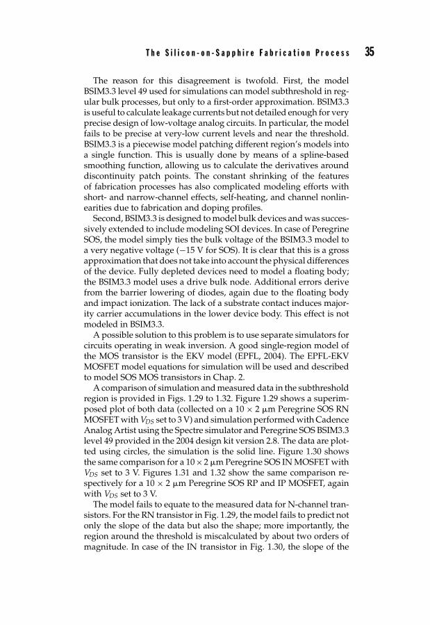
The reason for this disagreement is twofold. First, the modelBSIM3.3 level 49 used for simulations can model subthreshold in reg-ular bulk processes, but only to a first-order approximation. BSIM3.3is useful to calculate leakage currents but not detailed enough for veryprecise design of low-voltage analog circuits. In particular, the modelfails to be precise at very-low current levels and near the threshold.BSIM3.3 is a piecewise model patching different region’s models intoa single function. This is usually done by means of a spline-basedsmoothing function, allowing us to calculate the derivatives arounddiscontinuity patch points. The constant shrinking of the featuresof fabrication processes has also complicated modeling efforts withshort- and narrow-channel effects, self-heating, and channel nonlin-earities due to fabrication and doping profiles.
Second, BSIM3.3 is designed to model bulk devices and was succes-sively extended to include modeling SOI devices. In case of PeregrineSOS, the model simply ties the bulk voltage of the BSIM3.3 model toa very negative voltage (−15 V for SOS). It is clear that this is a grossapproximation that does not take into account the physical differencesof the device. Fully depleted devices need to model a floating body;the BSIM3.3 model uses a drive bulk node. Additional errors derivefrom the barrier lowering of diodes, again due to the floating bodyand impact ionization. The lack of a substrate contact induces major-ity carrier accumulations in the lower device body. This effect is notmodeled in BSIM3.3.
A possible solution to this problem is to use separate simulators forcircuits operating in weak inversion. A good single-region model ofthe MOS transistor is the EKV model (EPFL, 2004). The EPFL-EKVMOSFET model equations for simulation will be used and describedto model SOS MOS transistors in Chap. 2.
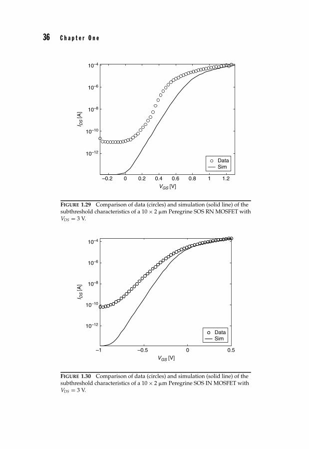
A comparison of simulation and measured data in the subthresholdregion is provided in Figs. 1.29 to 1.32. Figure 1.29 shows a superim-posed plot of both data (collected on a 10 × 2 �m Peregrine SOS RNMOSFET with VDS set to 3 V) and simulation performed with CadenceAnalog Artist using the Spectre simulator and Peregrine SOS BSIM3.3level 49 provided in the 2004 design kit version 2.8. The data are plot-ted using circles, the simulation is the solid line. Figure 1.30 showsthe same comparison for a 10×2 �m Peregrine SOS IN MOSFET withVDS set to 3 V. Figures 1.31 and 1.32 show the same comparison re-spectively for a 10 × 2 �m Peregrine SOS RP and IP MOSFET, againwith VDS set to 3 V.
The model fails to equate to the measured data for N-channel tran-sistors. For the RN transistor in Fig. 1.29, the model fails to predict notonly the slope of the data but also the shape; more importantly, theregion around the threshold is miscalculated by about two orders ofmagnitude. In case of the IN transistor in Fig. 1.30, the slope of the
July 8, 2009 14:4 Culurciello/Silicon-on-Sapphire Circuits and Systems/Eugenio Culurciello /160848-6/Ch01
36 C h a p t e r O n e
0–0.2 0.2 0.4 0.6 0.8 1 1.2
10–12
10–10
10–8
10–6
10–4
VGS [V]
I DS [A
]
DataSim
FIGURE 1.29 Comparison of data (circles) and simulation (solid line) of thesubthreshold characteristics of a 10 × 2 �m Peregrine SOS RN MOSFET withVDS = 3 V.
0–0.5–1 0.5
10–12
10–10
10–8
10–6
10–4
VGS [V]
I DS [A
]
DataSim
FIGURE 1.30 Comparison of data (circles) and simulation (solid line) of thesubthreshold characteristics of a 10 × 2 �m Peregrine SOS IN MOSFET withVDS = 3 V.

July 8, 2009 14:4 Culurciello/Silicon-on-Sapphire Circuits and Systems/Eugenio Culurciello /160848-6/Ch01
T h e S i l i c o n - o n - S a p p h i r e F a b r i c a t i o n P r o c e s s 37
0–0.5–1–1.5
–10–8
–10–6
–10–10
–10–12
VGS [V]
I DS [A
]
DataSim
FIGURE 1.31 Comparison of data (circles) and simulation (solid line) of thesubthreshold characteristics of a 10 × 2 �m Peregrine SOS RP MOSFET withVDS = 3 V.
0 0.5–0.5 1 1.5
–10–8
–10–6
–10–10
–10–12
VGS [V]
I DS [A
]
DataSim
FIGURE 1.32 Comparison of data (circles) and simulation (solid line) of thesubthreshold characteristics of a 10 × 2 �m Peregrine SOS IP MOSFET withVDS = 3 V.
July 8, 2009 14:4 Culurciello/Silicon-on-Sapphire Circuits and Systems/Eugenio Culurciello /160848-6/Ch01
38 C h a p t e r O n e
curve is miscalculated, producing an error of four orders of magnitude(!) for low current levels.
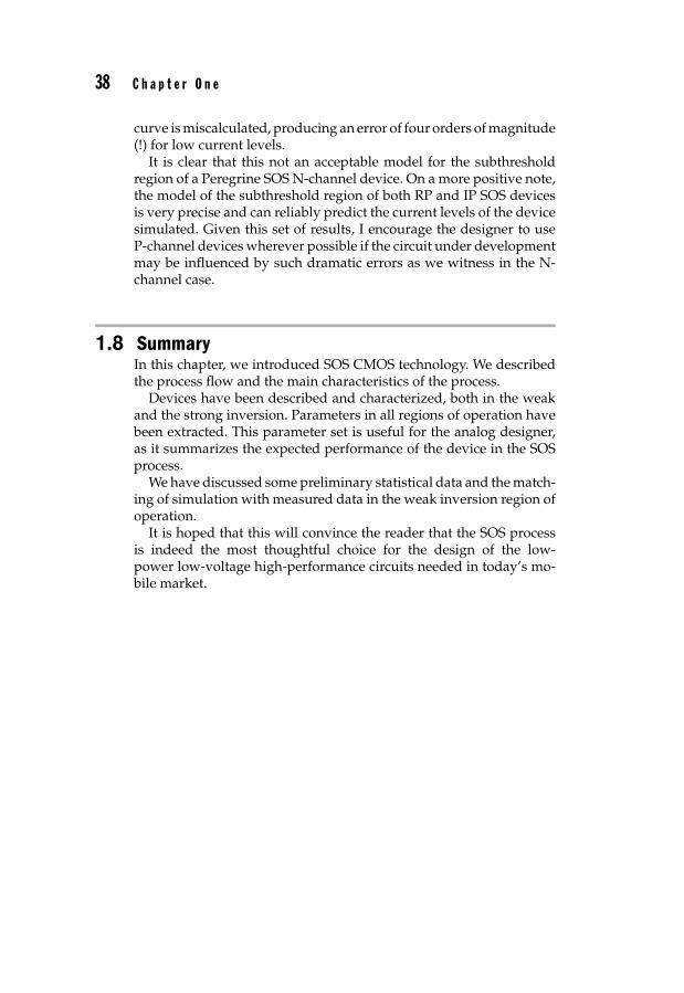
It is clear that this not an acceptable model for the subthresholdregion of a Peregrine SOS N-channel device. On a more positive note,the model of the subthreshold region of both RP and IP SOS devicesis very precise and can reliably predict the current levels of the devicesimulated. Given this set of results, I encourage the designer to useP-channel devices wherever possible if the circuit under developmentmay be influenced by such dramatic errors as we witness in the N-channel case.
1.8 SummaryIn this chapter, we introduced SOS CMOS technology. We describedthe process flow and the main characteristics of the process.
Devices have been described and characterized, both in the weakand the strong inversion. Parameters in all regions of operation havebeen extracted. This parameter set is useful for the analog designer,as it summarizes the expected performance of the device in the SOSprocess.
We have discussed some preliminary statistical data and the match-ing of simulation with measured data in the weak inversion region ofoperation.
It is hoped that this will convince the reader that the SOS processis indeed the most thoughtful choice for the design of the low-power low-voltage high-performance circuits needed in today’s mo-bile market.