Fabrication and Characterization of Pseudo-MOSFETs · creased mobility. In particular, strained...
12
Fabrication and Characterization of Pseudo-MOSFETs Joachim Knoch February 8, 2010 Contents 1 Introduction 2 2 The pseudo-MOSFET 3 3 Device Fabrication 5 4 Electrical Measurement and Characterization 8 5 Writing your Report 9 1
-
Upload
truongquynh -
Category
Documents
-
view
215 -
download
0
Transcript of Fabrication and Characterization of Pseudo-MOSFETs · creased mobility. In particular, strained...

Fabrication and Characterization ofPseudo-MOSFETs
Joachim Knoch
February 8, 2010
Contents
1 Introduction 2
2 The pseudo-MOSFET 3
3 Device Fabrication 5
4 Electrical Measurement and Characterization 8
5 Writing your Report 9
1

1 Introduction
Microelectronics has undergone an enormous development in recent years withan ever increasing performance of integrated circuits. This development has beenmade possible by modern CMOS technology, notably the down-scaling of transis-tor dimensions that leads to an exponentially increasing number of transistors ona chip, known as the famous Moor’s law. Figure 1 shows a schematics of a con-ventional n-type bulk-Si MOSFET consisting of highly n-type doped source anddrain areas within a p-type substrate. In addition, a MOSFET features a gateelectrode of length L and width W that is insulated from the bulk-Si substrate byan insulator (typically SiO2) of thickness dox. The two p-n-junctions will preventcurrent flow from source to drain. Applying a gate voltage Vgs across an insulatinggate oxide at the channel, the carrier concentration at the channel/gate interfacecan be controlled from accumulating the channel majority carriers through de-pleting free carriers to accumulation of channel minority carriers (inversion). Inthe case of inversion, current can flow from source to drain. The saturationcurrent through a MOSFET is to first order given by the following expression:
Id ≈ µeffW
LCox
(Vgs − Vth)2
2(1)
where Cox = εox/dox is the geometrical oxide capacitance per unit area, µeff isthe effective carrier mobility and Vgs,th are the gate and threshold voltages, re-spectively. Obviously, a higher current (which translates into a faster performingintegrated circuit) is obtained when the channel L length is scaled down and/orthe effective carrier mobility is increased. In the past, a performance increaseof MOSFET devices has almost exclusively been obtained by (down-)scaling thetransistor dimensions. However, in the very near future continuing the down-scaling will become difficult due to a number of issues. One of the major obsta-cles is related to the appearance of so-called short channel effects (SCE), i.e. aloss of electrostatic gate control over the potential in the channel region. Shortchannel effects arise due to an overlap of the source-channel and channel-drainp-n-junctions yielding a strongly reduced potential barrier as illustrated in Fig. 1(b). SCE are deleterious since they lead to drastically increased off-state leakagecurrents and thus to an enormous increase of power consumption of highly inte-grated circuits. Therefore, the semiconductor industry - notably AMD and IBM- have replaced the traditional bulk-Si substrates with silicon-on-insulator (SOI)technology. SOI substrates consist of a thin silicon layer of thickness dSOI on topof a so-called buried oxide (BOX) of thickness dbox. A major benefit of SOI is thatshort channel effects can be suppressed effectively by scaling down the SOI-layerthickness dSOI enabling a more drastic down-scaling of the channel length thanpossible with bulk-Si technology. If at the same time the effective carrier mobilitycould be increased, a strongly improved device performance is obtained. Recently,strain-silicon has been introduced as a “new” silicon material with up to 100% in-
2

creased mobility. In particular, strained silicon-on-insulator has attracted a greatdeal of interest since it allows combining scalability and transistor improvementsdue to the higher mobility. However, when fabricating the appropriate strained-SOI substrates it is indispensable to constantly measure the carrier mobility in afield-effect transistor device. This requirement calls for a fast turn-around devicecharacterization method. To this end so-called Pseudo-MOSFETs are fabricatedfor extraction of the carrier mobility which will be explained in detail below. Inthe present lab-training, such Pseudo-MOSFET devices with different contactingschemes will be fabricated, measured and characterized.
p-silicon
gate
n++ n++
L
source drain
doxW
Vgs
Vds
y
xz
(a) (b)
source channelsource drain drain
gate
E (
a.u
.)
λ
L
EL
∆Φf0
Figure 1: (a) Schematics of a conventional bulk-Si MOSFET. (b) Illustration of the appear-ance of short channel effects in a scaled device: the white line represents the conduction bandalong current transport direction in a long-channel device. In a device suffering from SCE, thesource-channel and channel-drain p-n-junctions overlap leading to a lowering of the potentialbarrier in the channel (green solid line). As a result, devices exhibiting SCE show an expo-nentially increased off-state leakage leading to a drastic increase of power consumption andeventually a loss of the ability to switch the device.
2 The pseudo-MOSFET
In SOI substrates the active silicon layer is separated from a silicon handle waferby a (rather thick) oxide, called the buried oxide (BOX). Therefore the idea ofthe pseudo-MOSFET is to use this buried oxide as the actual gate oxide and thesilicon handle wafer as the gate electrode. In this case, only source and draincontacts have to be defined in order to realize a MOSFET structure. Hence,the pseudo-MOSFET concept allows a quick and straight forwards realization ofMOSFETs and is therefore widely used to characterize SOI material. In orderto characterize the SOI material, in particular with respect to their mobility, asimple model for the current through a MOSFET is employed: For small Vds thedrain current Id increases linearly with drain voltage. In this so called linearregime of the output characteristics (i.e. Id versus drain-source voltage (Vds) for
3

different gate voltages Vgs) the current is given by
Id = fgCoxµ
1 + θ(Vgs − Vth)· (Vgs − Vth)Vds. (2)
Again, Cox = ϵ0ϵoxdox
is the gate oxide capacitance per unit area and dox is thegate oxide thickness, i.e. buried oxide thickness. Vth is the threshold voltage,i.e. the gate voltage where the device switches from the off- to the on-stateand fg is a factor that accounts for the geometry of the device. The factor θtakes series resistances into account, and is considered independent of the gatevoltage. Figure 2 (a) and (b) show the output and transfer characteristics ofa MOSFET. An important figure of merit of a MOSFET in the on-state is theso-called transconductance gm giving the amount of drain current change withaltering gate voltage:
gm =∂Id(Vds = const.)
∂Vgs
(3)
Vds(a.u.)
non-saturation saturation
I d(a
.u.)
Vg1
Vg2
Vg3
Vg4
100
10-2
10-4
10-6
10-8
0 0.5 1 1.5 2 2.5 30
0.2
0.4
0.6
0.8
I d(a
.u.)
log
(I )
d(a
.u.)
Vgs~Vth
(V)
subth
reshold
sw
ing
output characteristics transfer characteristics(a) (b)
Figure 2: Schematic cross section (a), output (b) and transfer (c) characteristics of a MOS-FET.
The quality of the SOI material is reflected in the electronic transport proper-ties of the material, i.e. in the effective carrier mobility µ. In order to determinethe mobility µ from the device characteristics we use the so-called Id/
√gm-method
which is particularly useful since it provides values for µ which are not influencedby parasitic series resistances. It is now easy to show that√
fgµCoxVds(Vgs − Vth) =Id√gm
(4)
Therefore, measuring Id versus Vgs at small drain-source bias (typically 0.05 to0.1V), calculating gm and plotting Id/
√gm versus Vgs yields a straight line. The
4

slope of this line is simply√fgµCoxVds from which the mobility µ can be extracted
provided that the geometry factor fg is known. In rectangular MOSFETs fg isthe ratio of channel width and channel length fg = W/L. However, since in ourexperiment we deal with circular pseudo-MOSFETs the geometry factor is a littlemore complicated. Nevertheless, a closed expression for the ratio between widthand length can be computed also in the circular case: fg =
2πln(R/r)
where R, r areradii of the circular pseudo-MOSFET as shown in Fig. 5.
3 Device Fabrication
The fabrication of the devices will be carried out in the central clean room facilityof the IMS. All participants have to wear a full cover with hoods, gowns andboots. The advisor will instruct the participants how to dress and how to behavein the clean room. Since the work will be done in the central facility great carehas to be taken. In particular, contamination is a severe issue and thereforethe participants have to wear gloves at all times when being in the clean room.Protective clothing such as apron, a second pair of gloves with sleeves and a faceshield is mandatory when working with hazardous chemicals.
Each participant will get three SOI samples. In addition, a bulk silicon sub-strate will be cleaved and every participant will get as many dummy samples asneeded. The fabrication procedure is listed below. During your lab-work, proto-col the fabrication process and take as many notes as necessary since this will beattached to the written report as an appendix.Mesa definition:
• a bulk silicon wafer is coated with HMDS and photoresist, pre-baked ona hot plate at 100◦C for 45s and subsequently cleaved into 2x2 cm2 pieceswith a diamond scribe.
• remove the photoresist with acetone, rinse in propanol
• dehydration of the samples on a hot plate at 115◦C for 5 minutes
• apply primer HMDS
• resist (AZ 1505) spin-on at 4200 rpm; pre-bake on a hot plate at 100◦C for45s
• 1st lithography with mask-aligner: expose the sample with 7mW/cm2 for15s
• develop for 30s (MIF:H20=1:1), rinse thoroughly in DI water
• post-exposure bake on hot plate at 100◦ for 5 minutes
5

• for mesa etching mix 50ml H2O, 100ml HNO3 and 5ml BOE (bufferedoxide etch). Note the order of the chemicals!! Caution: BOE containshydroflouric acid (HF), an extremely hazardous chemical that can lead tosevere injuries.
• determine the etch rate of the chemical solution by etching dummy sam-ples for several different durations, remove the resist in acetone, rinse inpropanol, blow dry with nitrogen and measure the etch depth with a sur-face profiler
• determine expected etch duration, etch the SOI sample until you see thatall SOI is gone and rinse immediately afterwards in DI water
• remove the photoresist in acetone, rinse in propanol, blow dry
Si
SOI
SiO2
Si
SiO2
photoresist
Si
SiO2
Figure 3: Schematics of the mesa etch process.
Contact configuration 1
• clean samples in Piranha
• remove the native oxide on the mesa (the circular mesa consists of SOI)of sample no. 1 with BOE, rinse for a few minutes and then immediatelymount the sample into the sputter deposition tool.
• deposit 200nm Al.
• dehydration of sample no. 1 on a hot plate at 115◦C for 5 minutes
• apply primer HMDS
• resist (AZ 1505) spin-on at 4200 rpm; pre-bake on a hot plate at 100◦C for45s
• 2nd lithography, expose as stated above
• develop for 30s (see above), rinse thoroughly in DI water
• post-exposure bake on hot plate at 100◦ for 5 minutes
6

• etch Al in PAN-etch
• remove resist in acetone, rinse in propanol and blow dry with nitrogen
Contact configuration 2
• dehydration of sample on a hot plate at 115◦C for 5 minutes
• apply primer HMDS
• resist (AZ 5214) spin-on at 4200 rpm; pre-bake on a hot plate at 100◦C for45s
• 2nd lithography, image reversal process. Expose the samples for 10s fol-lowed by a post-exposure bake on the hot plate at 115◦ for 90s; flood expo-sure for 20s.
• develop in undiluted developer for 30s, rinse thoroughly in DI water
• dip in BOE solution for 10s, rinse in DI water for 2 minutes, the samples arethen mounted in an e-beam evaporation chamber and aluminum (200nm)is deposited.
• put the samples in acetone, lift-off aluminum, rinse in propanol and blowdry with nitrogen
Contact configuration 3
• samples will be cleaned in Piranha (sulfuric acid/hydrogen peroxide mix-ture) for 10min at 65◦. Rinse thoroughly in DI water, blow dry with nitro-gen.
• mount the samples in PECVD tool, deposit 100nm SiO2 at 300◦C.
• dehydration of sample on a hot plate at 115◦C for 5 minutes
• apply primer HMDS
• resist (AZ 1505) spin-on at 4200 rpm; pre-bake on a hot plate at 100◦C for45s
• 2nd lithography as in “contact configuration 1”.
• develop for 30s (see above), rinse thoroughly in DI water
• using BOE etch all SiO2, rinse in DI water, blow dry
• remove resist in acetone, rinse in propanol, blow dry
7

• dip samples in BOE for 10s, rinse in DI water for 2 minutes, the samplesare then mounted in the sputter tool and 100nm Ni is deposited.
• anneal samples in nitrogen atmosphere in an RTA at 500◦C for 1min
• etch away superficial Ni in Piranha (see above).
Al
Al
Si
SiO2
Si
SiO2
Si
SiO2
SiN
Si
SiO2
Si
SiO2
Si
SiO2
Al
resist
resist
SOI
Si
SiO2
Ni
SOI
Si
SiO2
SOI
contact formation 1
contact formation 2
contact formation 3
Si
SiO2
NiSi
Figure 4: Schematics of the three different contact configurations.
Figure 5 shows a scanning electron microscopy image of a readily fabricatedcircular pseudo-MOSFET. The width and channel length of the device are shownas well. The buried oxide (BOX) serves as the actual gate oxide as alreadymentioned above.
4 Electrical Measurement and Characterization
Electrical measurements will be performed with an Hewlett Packard Semicon-ductor Parameter Analyser. The sample will be mounted in a probe station as
8

Si back-gate
BOX
source
drain
dBOX
L
W
Al
Si back-gate
BOXdBOX
r
R
dV
sV
gsV
Figure 5: Microscope image of a fabricated pseudo MOSFET.
schematically shown in Fig. 6. The following measurements and characterizationsshould be made:
• Measure (all devices) the drain current versus gate voltage (transfer char-acteristics) over a large gate voltage range (e.g. ±40V) for drain voltagesof up to 2V starting at 0.1V. Plot the transfer characteristics on a linearand a log-scale plot. Compare the on-currents, the leakage currents due tothe ambipolar behavior and the inverse subthreshold slopes of the differentdevices.
• Measure (all devices) the output characteristics over the same drain andgate voltage range. Plot the output characteristics.
• Extract the mobility of the fabricated samples using the Id/√gm-method.
Plot the mobility versus the channel length of the different devices.
5 Writing your Report
After the characterization you are supposed to write a short report. Since writingreports is often considered as being boring you should write it with the followingbackground:
After finishing your BSc/MSc degree at TU Dortmund University you work foran up-and-coming consulting company in the semiconductor industry. Your spe-ciality is the implementation of new materials into existing CMOS productionlines and you have been called by the CTO (chief technical officer) - one of your
9
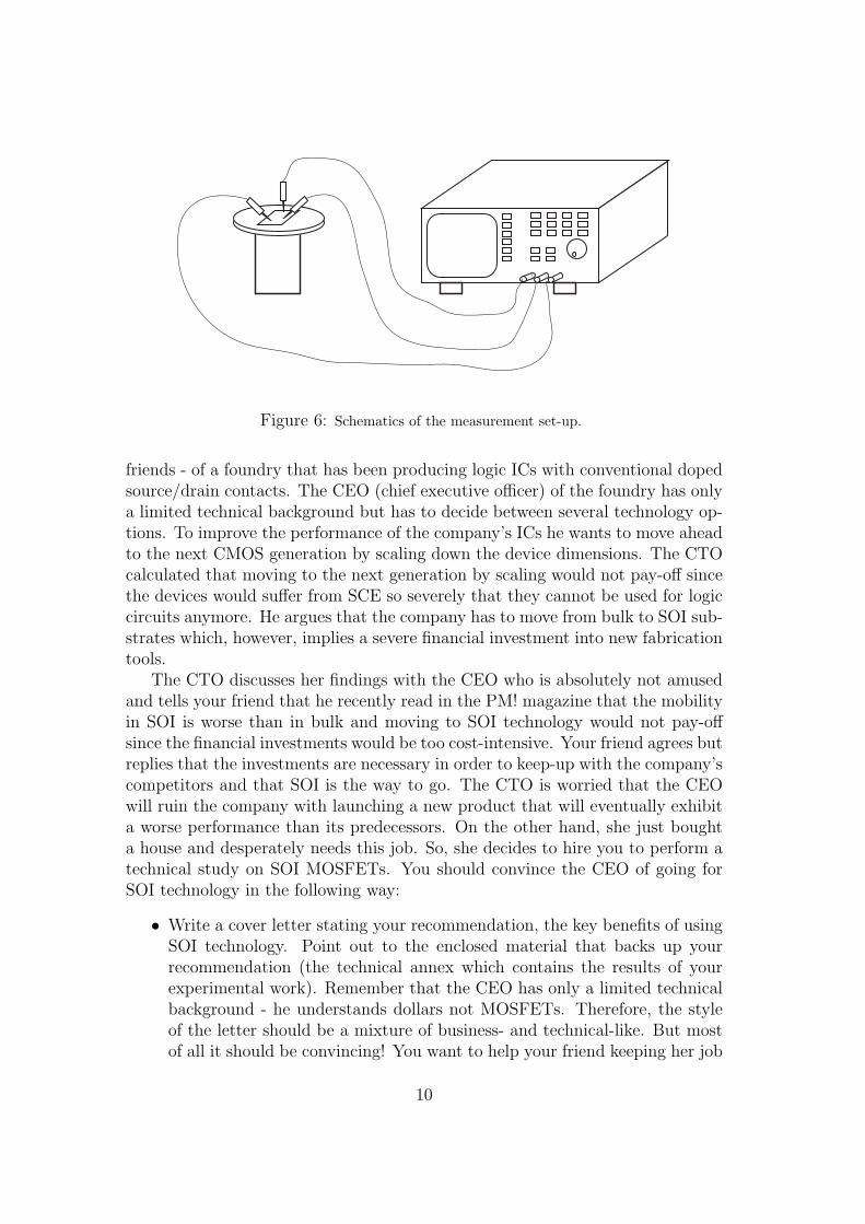
Figure 6: Schematics of the measurement set-up.
friends - of a foundry that has been producing logic ICs with conventional dopedsource/drain contacts. The CEO (chief executive officer) of the foundry has onlya limited technical background but has to decide between several technology op-tions. To improve the performance of the company’s ICs he wants to move aheadto the next CMOS generation by scaling down the device dimensions. The CTOcalculated that moving to the next generation by scaling would not pay-off sincethe devices would suffer from SCE so severely that they cannot be used for logiccircuits anymore. He argues that the company has to move from bulk to SOI sub-strates which, however, implies a severe financial investment into new fabricationtools.
The CTO discusses her findings with the CEO who is absolutely not amusedand tells your friend that he recently read in the PM! magazine that the mobilityin SOI is worse than in bulk and moving to SOI technology would not pay-offsince the financial investments would be too cost-intensive. Your friend agrees butreplies that the investments are necessary in order to keep-up with the company’scompetitors and that SOI is the way to go. The CTO is worried that the CEOwill ruin the company with launching a new product that will eventually exhibita worse performance than its predecessors. On the other hand, she just boughta house and desperately needs this job. So, she decides to hire you to perform atechnical study on SOI MOSFETs. You should convince the CEO of going forSOI technology in the following way:
• Write a cover letter stating your recommendation, the key benefits of usingSOI technology. Point out to the enclosed material that backs up yourrecommendation (the technical annex which contains the results of yourexperimental work). Remember that the CEO has only a limited technicalbackground - he understands dollars not MOSFETs. Therefore, the styleof the letter should be a mixture of business- and technical-like. But mostof all it should be convincing! You want to help your friend keeping her job
10
(You might want to use this opportunity to give your consulting companya fancy name.)!
• Prepare a technical annex. In this annex you should explain and discussthe pseudo-MOSFET results. You should also state and explain shortlythe method you used to obtain the mobility data and the experimentalprocedure. To this annex your lab notes should be added. Refer to thesenotes in the technical annex.
The report can either be written in German or English.
Bibliography
• M.S. Sze, “Physics of Semiconductor Devices”, John Wiley& Sons Inc.,1981.
• Y. Taur and T.H. Ning, “Fundamentals of Modern VLSI Devices ”, Cam-bridge University Press, 1998.
• J.-P. Colinge, “Silicon-on-Insulator Technology: Materials to VLSI ”, KluwerAcademic Publisher, 2004.
11

1 2 3
4
5
6
7
8 9
10
1112 13
1: R=3350µm, r=300µm2: R=2900µm, r=300µm3: R=2900µm, r=790µm4: R=975µm, r=100µm5: R=975µm, r=287µm6: R=850µm, r=300µm7: R=1280µm, r=300µm8: R=1800µm, r=790µm9: R=1800µm, r=200µm10: R=975µm, r=195µm11: R=3350µm, r=270µm12: R=2900µm, r=300µm13: R=2900µm, r=790µm