AS1530, AS1531 Data Sheet - Digi-Key Sheets... · · 2013-11-25 Revision 1.02 2 - 29...
29
AS1530, AS1531 12-Bit, Single-Supply, Low-Power, 400/300ksps, 8-Channel A/D Converters Data Sheet www.austriamicrosystems.com Revision 1.02 1 - 29 1 General Description The AS1530/AS1531 are low-power,8/4-channel, 400/ 300ksps, 12-bit analog-to-digital (A/D) converters specif- ically designed to operate with single-supply devices. Superior AC characteristics, very low power consump- tion, and highly-reliable packaging make these ultra- small devices perfect for battery-powered remote-sen- sor and data-acquisition devices. The successive-approximation register (SAR), high- speed sampling, high-bandwidth track/hold circuitry, and multi-mode operation combine to make these devices highly-flexible and configurable. Both devices require low supply current (2.8mA @ 400ksps, AS1530; 2.2mA @ 300ksps, AS1531) and fea- ture a reduced-power mode and a power-down mode to lower power consumption at slower throughput rates. The devices operate from a single supply (+4.5 to +5.5V, AS1530; +2.7 to +3.6V, AS1531). Both devices contain an internal 2.5V reference, an integrated reference buffer, and feature support for an external reference (1V to VDD). Data accesses are made via the high-speed, 4-wire, SPI, QSPI-, and Microwire-compatible serial interface. The devices are available in a 20-pin TSSOP package. Figure 1. Block Diagram and Pin Assignments 2 Key Features ! Single-Supply Operation: - +4.5 to +5.5V (AS1530) - +2.7 to +3.6V (AS1531) ! Sampling Rate: - 400ksps (AS1530) - 300ksps (AS1531) ! Software-Configurable Analog Input Types: - 8-Channel Single-Ended - 8-Channel Pseudo Differential Referenced to COM - 4-Channel Pseudo Differential - 4-Channel Fully Differential ! Software-Configurable Input Range ! Internal +2.5V Reference ! Low-Current Operation: - 2.8mA @ 400ksps (AS1530) - 2.2mA @ 300ksps (AS1531) - 0.4mA in Reduced-Power Mode - 0.5μA in Full Power-Down Mode ! SPI/QSPI/Microwire/TMS320-Compatible ! 20-pin TSSOP Package 3 Applications The devices are ideal for remote sensors, data-acquisi- tion and data-logging devices, pen-digitizers, process control, or any other space-limited A/D application with low power-consumption requirements. AS1530/ AS1531 Control Logic Output Shift Register 12-Bit SAR IN OUT REF Analog Input +1.2V REF Input Shift Register Track/ Hold 17kΩ Av ≈ 2.05 +2.50V 15 SSTRB 17 CSN 14 DOUT 20 VDD1 19 VDD2 13 GND 18 SCLK 16 DIN 1:8 CH0:CH7 9 COM 12 REFADJ 11 REF 10 VDD3 AS1530/ AS1531 1 CH0 2 CH1 3 CH2 4 CH3 5 CH4 6 CH5 7 CH6 8 CH7 9 COM 10 VDD3 20 VDD1 19 VDD2 18 SCLK 17 CSN 16 DIN 15 SSTRB 14 DOUT 13 GND 12 REFADJ 11 REF
Transcript of AS1530, AS1531 Data Sheet - Digi-Key Sheets... · · 2013-11-25 Revision 1.02 2 - 29...

AS1530, AS1531 12-Bit , Single-Supply, Low-Power, 400/300ksps, 8-Channel A/D Converters
Data Sheet
1 General DescriptionThe AS1530/AS1531 are low-power,8/4-channel, 400/300ksps, 12-bit analog-to-digital (A/D) converters specif-ically designed to operate with single-supply devices. Superior AC characteristics, very low power consump-tion, and highly-reliable packaging make these ultra-small devices perfect for battery-powered remote-sen-sor and data-acquisition devices.
The successive-approximation register (SAR), high-speed sampling, high-bandwidth track/hold circuitry, and multi-mode operation combine to make these devices highly-flexible and configurable.
Both devices require low supply current (2.8mA @ 400ksps, AS1530; 2.2mA @ 300ksps, AS1531) and fea-ture a reduced-power mode and a power-down mode to lower power consumption at slower throughput rates.
The devices operate from a single supply (+4.5 to +5.5V, AS1530; +2.7 to +3.6V, AS1531). Both devices contain an internal 2.5V reference, an integrated reference buffer, and feature support for an external reference (1V to VDD).
Data accesses are made via the high-speed, 4-wire, SPI, QSPI-, and Microwire-compatible serial interface.
The devices are available in a 20-pin TSSOP package.
Figure 1. Block Diagram and Pin Assignments
2 Key Features! Single-Supply Operation:
- +4.5 to +5.5V (AS1530)- +2.7 to +3.6V (AS1531)
! Sampling Rate:- 400ksps (AS1530)- 300ksps (AS1531)
! Software-Configurable Analog Input Types:- 8-Channel Single-Ended- 8-Channel Pseudo Differential Referenced to COM- 4-Channel Pseudo Differential- 4-Channel Fully Differential
! Software-Configurable Input Range! Internal +2.5V Reference! Low-Current Operation:
- 2.8mA @ 400ksps (AS1530)- 2.2mA @ 300ksps (AS1531)- 0.4mA in Reduced-Power Mode- 0.5µA in Full Power-Down Mode
! SPI/QSPI/Microwire/TMS320-Compatible! 20-pin TSSOP Package
3 ApplicationsThe devices are ideal for remote sensors, data-acquisi-tion and data-logging devices, pen-digitizers, process control, or any other space-limited A/D application with low power-consumption requirements.
AS1530/AS1531
ControlLogic
OutputShift
Register
12-BitSAR
IN OUTREF
Analog Input
+1.2VREF
Input ShiftRegister
Track/Hold
17kΩ
Av ≈ 2.05
+2.50V
15
SSTRB
17
CSN
14
DOUT
20
VDD1
19
VDD2
13
GND
18
SCLK16
DIN
1:8
CH0:CH79
COM
12
REFADJ11
REF
10
VDD3
AS1530/AS1531
1CH0
2CH1
3CH2
4CH3
5CH4
6CH5
7CH6
8CH7
9COM
10VDD3
20 VDD1
19 VDD2
18 SCLK
17 CSN
16 DIN
15 SSTRB
14 DOUT
13 GND
12 REFADJ
11 REF
www.austriamicrosystems.com Revision 1.02 1 - 29

AS1530/AS1531Data Sheet
Contents1 General Description ................................................................................................................................ 12 Key Features .......................................................................................................................................... 13 Applications ............................................................................................................................................ 14 Pinout ..................................................................................................................................................... 3
Pin Assignments ..................................................................................................................................................... 3Pin Descriptions ..................................................................................................................................................... 3
5 Absolute Maximum Ratings .................................................................................................................... 46 Electrical Characteristics ........................................................................................................................ 5
AS1530 Electrical Characteristics .......................................................................................................................... 5AS1531 Electrical Characteristics .......................................................................................................................... 7Timing Characteristics ............................................................................................................................................ 9
7 Typical Operating Characteristics ......................................................................................................... 118 Detailed Description ............................................................................................................................. 14
Analog Input ......................................................................................................................................................... 14Input Protection ............................................................................................................................................. 14
Track/Hold ............................................................................................................................................................ 14Control Register ................................................................................................................................................... 15Analog Input Configuration ................................................................................................................................... 15Channel Selection ................................................................................................................................................ 16
Single-Ended Input ........................................................................................................................................ 16Differential Input ............................................................................................................................................ 16
Starting a Conversion ........................................................................................................................................... 17Transfer Functions ................................................................................................................................................ 18Power Modes ....................................................................................................................................................... 19
Reduced Power Mode ................................................................................................................................... 20Full Power-Down Mode ................................................................................................................................. 20
Reference ............................................................................................................................................................. 21Internal Reference ......................................................................................................................................... 21External Reference ....................................................................................................................................... 22
9 Application Information ......................................................................................................................... 23Initialization ........................................................................................................................................................... 23Serial Interface ..................................................................................................................................................... 23
Serial Interface Configuration ........................................................................................................................ 23QSPI Interface ............................................................................................................................................... 24
Quick Evaluation Circuit ....................................................................................................................................... 25Layout Considerations .......................................................................................................................................... 26
10 Package Drawings and Markings ....................................................................................................... 2711 Ordering Information ........................................................................................................................... 28
www.austriamicrosystems.com Revision 1.02 2 - 29

AS1530/AS1531Data Sheet - P inou t
4 PinoutPin AssignmentsFigure 2. Pin Assignments (Top View)
Pin DescriptionsTable 1. Pin Descriptions
Pin Number Pin Name Description1:8 CH0:CH7 Analog Sampling Inputs. These eight pins serve as analog sampling inputs.
9 COM Common Analog Inputs. Tie this pin to ground in single-ended mode.
10 VDD3 Positive Supply Voltage
11 REF
Reference-Buffer Output/A/DC Reference Input. This pin serves as the reference voltage for analog-to-digital conversions. In internal reference mode, the reference buffer provides a +2.50V nominal output, externally adjustable at pin REFADJ. In external reference mode, disable the internal buffer by pulling pin REFADJ to VDD1.
12 REFADJReference-Buffer Amplifier Input. To disable the reference-buffer amplifier, tie this pin to VDD1.
13 GND Analog and Digital Ground
14 DOUTSerial Data Output. Data is clocked out at the rising edge of pin SCLK. DOUT is high impedance when CSN is high.
15 SSTRBSerial Strobe Output. SSTRB pulses high for one clock period before the MSB is clocked out. SSTRB is high impedance when CSN is high.
16 DIN Serial Data Input. Data is clocked in at the rising edge of SCLK.
17 CSNActive-Low Chip Select. Data will not be clocked into pin DIN unless CSN is low. When CSN is high, pins DOUT and SSTRB are high impedance.
18 SCLKSerial Clock Input. This pin clocks data into and out of the serial interface, and is used to set the conversion speed. Note: The duty cycle must be between 40 and 60%.
19 VDD2 Positive Supply Voltage20 VDD1 Positive Supply Voltage
AS1530/AS1531
1CH0
2CH1
3CH2
4CH3
5CH4
6CH5
7CH6
8CH7
9COM
10VDD3
20 VDD1
19 VDD2
18 SCLK
17 CSN
16 DIN
15 SSTRB
14 DOUT
13 GND
12 REFADJ
11 REF
www.austriamicrosystems.com Revision 1.02 3 - 29

AS1530/AS1531Data Sheet - Abso lu te Max imum Rat ings
5 Absolute Maximum RatingsStresses beyond those listed in Table 2 may cause permanent damage to the device. These are stress ratings only, and functional operation of the device at these or any other conditions beyond those indicated in Electrical Character-istics on page 5 is not implied. Exposure to absolute maximum rating conditions for extended periods may affect device reliability.
Table 2. Absolute Maximum Ratings
Parameter Min Max Units CommentsVDD1, VDD2, VDD3 to GND -0.3 +7 V
VDD1 to VDD2 to VDD3 -0.3 +0.3 V
CH0:CH7, COM to GND -0.3 VDD1 + +0.3 V
REF, REFADJ to GND -0.3 VDD1 + +0.3 V
DIN, SCLK, CSN, to GND -0.3 VDD2 + +0.3 V
DOUT, SSTRB to GND -0.3 VDD2 + +0.3 V
DOUT, SSTRB Sink Current 25 mA
Continuous Power Dissipation (TAMB = +70ºC) 559 mW Derate 7.0mW/ºC above +70ºC
Operating Temperature Range -40 +85 ºC
Storage Temperature Range -60 +150 ºC
Package Body Temperature +260 ºC
The reflow peak soldering temperature (body temperature) specified is in accordance with IPC/JEDEC J-STD-020C “Moisture/Reflow Sensitivity Classification for Non-Hermetic
Solid State Surface Mount Devices”.The lead finish for Pb-free leaded packages is
matte tin (100% Sn).
www.austriamicrosystems.com Revision 1.02 4 - 29

AS1530/AS1531Data Sheet - E lec t r i ca l Charac te r i s t i cs
6 Electrical CharacteristicsAS1530 Electrical Characteristics VDD1 = VDD2 = VDD3 = +4.5 to +5.5V, COM = GND, fSCLK= 6.4MHz, 50% duty cycle, 16 clocks/conversion cycle (400ksps), external +2.5V at REF, REFADJ = VDD1, TAMB = TMIN to TMAX (unless otherwise specified). Typ values at TAMB = +25ºC. Table 3. AS1530 Electrical Characteristics
Symbol Parameter Conditions Min Typ Max Units
DC Accuracy 1
Resolution 12 Bits INL Relative Accuracy 2 -1 +1 LSB DNL Differential Nonlinearity No missing codes over temperature -1 +1 LSB
Offset Error -6 +6 LSB
Gain Error 3 -6 +6 LSB Gain-Error Temperature
Coefficient ±1.6 ppm/°C
Channel-to-Channel Offset Error Matching ±0.2 LSB
Dynamic Specifications: 100kHz sinewave input, 2.5Vp-p, 400ksps, 6.4MHz clock, bit RANGE (page 15) = 0, pseudo-differential input mode
SINAD Signal-to-Noise plus Distortion Ratio 70 dB
THD Total Harmonic Distortion Up to the 5th harmonic -82 dB
SFDR Spurious-Free Dynamic Range 83 dB
IMD Intermodulation Distortion fIN1 = 99kHz, fIN2 = 102kHz 76 dB Channel-to-Channel
Crosstalk 4fIN = 200kHz, VIN = 2.5Vp-p -85 dB
Full-Power Bandwidth -3dB point 6 MHz Full-Linear Bandwidth SINAD > 68dB 450 kHz
Conversion Rate tCONV Conversion Time 5 2.5 µs tACQ Track/Hold Acquisition Time 390 ns tAD Aperture Delay 7 ns tAJ Aperture Jitter <50 ps
fSCLK Serial Clock Frequency 0.5 6.4 MHz Duty Cycle 40 60 %
Analog Inputs: CH0:CH7, COM
VCHx - VCHy
(COM)
Input Voltage Range: Single-Ended, Pseudo-Differential,
and Differential 6
Bit RANGE (page 15) = 1 0 VREF V
Bit RANGE (page 15) = 0 -VREF/2
+VREF/2
Multiplexer Leakage Current On/off leakage current, VCHx = 0 or VDD1 -1 ±0.001 +1 µA Input Capacitance 18 pF
Internal Reference VREF REF Output Voltage TAMB = +25ºC 2.48 2.50 2.52 V
REF Short-Circuit Current 30 mA
TCVREF REF Output Temperature Coefficient ±25 ppm/
°C
Load Regulation 7 0 to 1mA output load 1.2 4.0 mV/mA
CBYPREF Capacitive Bypass at REF 4.7 10 µF
www.austriamicrosystems.com Revision 1.02 5 - 29

AS1530/AS1531Data Sheet - E lec t r i ca l Charac te r i s t i cs
CBYPREFADJ
Capacitive Bypass at REFADJ 0.01 10 µF
REFADJ Output Voltage 1.22 V REFADJ Input Range For small adjustments, from 1.22V ±100 mV
REFADJ Buffer Disable Threshold To power down the internal reference 1.4 VDD1 -
1 V
Buffer Voltage Gain 2.045 V/V External Reference: Reference buffer disabled, reference applied to pin REF
REF Input Voltage Range 8 1.0 VDD1
+ 50mV
V
REF Input Current
VREF = 2.50V, fSCLK = 6.4MHz 200 350
µAVREF = 2.50V, fSCLK = 0 320 Power-Down, fSCLK = 0 5
Digital Inputs: DIN, SCLK, CSN
VINH Input High Voltage 0.7 x VDD V
VINL Input Low Voltage 0.3 x VDD V
VHYST Input Hysteresis 0.2 V IIN Input Leakage VIN = 0 or VDD2 -1 +1 µA CIN Input Capacitance 5 pF
Digital Outputs: DOUT, SSTRBVOL Output Voltage Low ISINK = 5mA 0.45 V VOH Output Voltage High ISOURCE = 1mA 4 V
IL Tri-State Leakage Current CSN = VDD2 -10 +10 µA COUT Tri-State Output Capacitance CSN = VDD2 5 pF
Power SupplyVDD1, VDD2, VDD3
Positive Supply Voltage 9 4.5 5.5 V
IVDD1, IVDD2, IVDD3
Supply Current VDD1 = VDD2 = VDD3 = 5.5V
Normal Operation with External Reference 10 2.8 3.3
mANormal Operation with Internal Reference 10 3.3 3.8
Reduced-Power Mode 11 0.4 0.8
Full Power-Down Mode 0.5 2 µA
PSR Power-Supply Rejection VDD1 = VDD2 = VDD3 = 5V ±10% -2 ±0.1 +2 mV
1. Tested at VDD1 = VDD2 = VDD3 = +5V, COM = GND, bit RANGE (page 15) = 1, single-ended input mode.2. Relative accuracy is the deviation of the analog value at any code from its theoretical value after the gain error
and offset error have been nulled.3. Offset nulled.4. Ground on channel; sinewave applied to all off channels.5. Conversion time is defined as the number of clock cycles multiplied by the clock period; clock has 50% duty
cycle.6. The absolute voltage range for the analog inputs (CH0:CH7, and COM) is from GND to VDD1. 7. External load should not change during conversion for specified accuracy. Guaranteed specification of 4mV/mA
is a result of production test limitations. 8. AS1530/AS1531 performance is limited by the device noise floor, typically 300µVp-p.
Table 3. AS1530 Electrical Characteristics (Continued)Symbol Parameter Conditions Min Typ Max Units
www.austriamicrosystems.com Revision 1.02 6 - 29

AS1530/AS1531Data Sheet - E lec t r i ca l Charac te r i s t i cs
AS1531 Electrical CharacteristicsVDD1 = VDD2 = VDD3 = +2.7 to +3.6V, COM = GND, fSCLK = 4.8MHz, 50% duty cycle, 16 clocks/conversion cycle (300ksps), external +2.5V at REF, REFADJ = VDD1, TAMB = TMIN to TMAX (unless otherwise specified). Typ values at TAMB = +25ºC.
9. Electrical characteristics are guaranteed from VDD1(MIN) = VDD2(MIN) = VDD3(MIN) to VDD1(MAX) = VDD2(MAX) = VDD3(MAX). For operations beyond this range, see Typical Operating Characteristics on page 11. For guaranteed specifications beyond the limits, contact austriamicrosystems, AG.
10. AIN = mid-scale; bit RANGE (page 15) = 1; tested with 20pF on DOUT, 20pF on SSTRB, and fSCLK = 6.4MHz @ GND to VDD2.
11. SCLK = DIN = GND, CSN = VDD2.
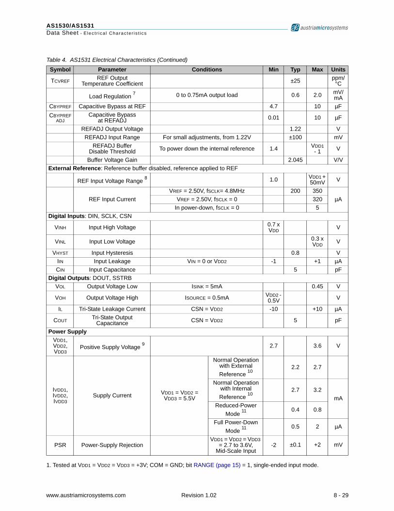
Table 4. AS1531 Electrical Characteristics
Symbol Parameter Conditions Min Typ Max Units
DC Accuracy 1
Resolution 12 Bits
INL Relative Accuracy 2 -1 +1 LSB
DNL Differential Nonlinearity No missing codes over temperature -1 +1 LSB Offset Error -6 +6 LSB
Gain Error 3 -6 +6 LSB
Gain-Error Temperature Coefficient ±1.6 ppm/
°C Channel-to-Channel Offset
Error Matching ±0.2 LSB
Dynamic Specifications: 75kHz sinewave input, 2.5Vp-p, 300ksps, 4.8MHz clock, bit RANGE (page 15) = 0, pseudo-differential input mode
SINAD Signal-to-Noise plus Distortion Ratio 70 dB
THD Total Harmonic Distortion Up to the 5th harmonic -81 dB
SFDR Spurious-Free Dynamic Range 84 dB
IMD Intermodulation Distortion fIN1 = 73kHz, fIN2 = 77kHz 76 dB Channel-to-Channel
Crosstalk 4fIN = 150kHz, VIN = 2.5Vp-p -80 dB
Full-Power Bandwidth -3dB point 6 MHz Full-Linear Bandwidth SINAD > 68dB 350 kHz
Conversion Rate tCONV Conversion Time 5 Normal operation 3.3 µs tACQ Track/Hold Acquisition Time Normal operation 520 ns tAD Aperture Delay 7 ns tAJ Aperture Jitter <50 ps
fSCLK Serial Clock Frequency Normal operation 0.5 4.8 MHz Duty Cycle 40 60 %
Analog Inputs: CH0:CH7, COM
VCHx - VCHy
(COM)
Input Voltage Range: Single-Ended, Pseudo-Differential,
and Differential 6
Bit RANGE (page 15) = 1 0 VREFV
Bit RANGE (page 15) = 0 -VREF/2
+VREF/2
Multiplexer Leakage Current On/off leakage current, VCHx = 0 or AVDD -1 ±0.001 +1 µA Input Capacitance 18 pF
Internal Reference VREF REF Output Voltage TAMB = +25°C 2.48 2.50 2.52 V
REF Short-Circuit Current 30 mA
www.austriamicrosystems.com Revision 1.02 7 - 29
AS1530/AS1531Data Sheet - E lec t r i ca l Charac te r i s t i cs
TCVREF REF Output Temperature Coefficient ±25 ppm/
°C
Load Regulation 7 0 to 0.75mA output load 0.6 2.0 mV/mA
CBYPREF Capacitive Bypass at REF 4.7 10 µF CBYPREF
ADJCapacitive Bypass
at REFADJ 0.01 10 µF
REFADJ Output Voltage 1.22 V REFADJ Input Range For small adjustments, from 1.22V ±100 mV
REFADJ Buffer Disable Threshold To power down the internal reference 1.4 VDD1
- 1 V
Buffer Voltage Gain 2.045 V/V External Reference: Reference buffer disabled, reference applied to REF
REF Input Voltage Range 8 1.0 VDD1 + 50mV V
REF Input CurrentVREF = 2.50V, fSCLK= 4.8MHz 200 350
µAVREF = 2.50V, fSCLK = 0 320 In power-down, fSCLK = 0 5
Digital Inputs: DIN, SCLK, CSN
VINH Input High Voltage 0.7 x VDD V
VINL Input Low Voltage 0.3 x VDD V
VHYST Input Hysteresis 0.8 V IIN Input Leakage VIN = 0 or VDD2 -1 +1 µA CIN Input Capacitance 5 pF
Digital Outputs: DOUT, SSTRBVOL Output Voltage Low ISINK = 5mA 0.45 V
VOH Output Voltage High ISOURCE = 0.5mA VDD2 - 0.5V V
IL Tri-State Leakage Current CSN = VDD2 -10 +10 µA
COUT Tri-State Output Capacitance CSN = VDD2 5 pF
Power Supply VDD1, VDD2, VDD3
Positive Supply Voltage 9 2.7 3.6 V
IVDD1, IVDD2, IVDD3
Supply Current VDD1 = VDD2 = VDD3 = 5.5V
Normal Operation with External Reference 10
2.2 2.7
Normal Operation with Internal Reference 10
2.7 3.2mA
Reduced-Power Mode 11 0.4 0.8
Full Power-Down Mode 11 0.5 2 µA
PSR Power-Supply RejectionVDD1 = VDD2 = VDD3
= 2.7 to 3.6V, Mid-Scale Input
-2 ±0.1 +2 mV
1. Tested at VDD1 = VDD2 = VDD3 = +3V; COM = GND; bit RANGE (page 15) = 1, single-ended input mode.
Table 4. AS1531 Electrical Characteristics (Continued)
Symbol Parameter Conditions Min Typ Max Units
www.austriamicrosystems.com Revision 1.02 8 - 29

AS1530/AS1531Data Sheet - E lec t r i ca l Charac te r i s t i cs
Timing Characteristics
2. Relative accuracy is the deviation of the analog value at any code from its theoretical value after the gain error and offset error have been nulled.
3. Offset nulled.4. Ground on channel; sinewave applied to all off channels.5. Conversion time is defined as the number of clock cycles multiplied by the clock period; clock has 50% duty
cycle.6. The absolute voltage range for the analog inputs (CH0:CH7, and COM) is from GND to VDD1.7. External load should not change during conversion for specified accuracy. Guaranteed specification of 2mV/mA
is a result of production test limitations.8. AS1530/AS1531 performance is limited by the device noise floor, typically 300µVp-p.9. Electrical characteristics are guaranteed from VDD1(MIN) = VDD2(MIN) = VDD3(MIN) to VDD1(MAX) = VDD2(MAX) =
VDD3(MAX). For operations beyond this range, see Typical Operating Characteristics on page 11. For guaranteed specifications beyond the limits, contact austriamicrosystems, AG.
10. AIN = mid-scale; bit RANGE (page 15) = 1; tested with 20pF on DOUT, 20pF on SSTRB, and fSCLK = 4.8MHz @ GND to VDD2.
11. SCLK = DIN = GND, CSN = VDD2.
Table 5. AS1530 Timing Characteristics – (Figures 3, 4, 21, 23; VDD1 = VDD2 = VDD3 = +4.5 to +5.5V; TAMB = TMIN to TMAX (unless otherwise specified).
Symbol Parameter Conditions Min Typ Max UnitstCP SCLK Period 156 ns tCH SCLK Pulse Width High 62 ns tCL SCLK Pulse Width Low 62 ns tDS DIN to SCLK Setup 35 ns tDH DIN to SCLK Hold 0 ns tCSS CSN Fall to SCLK Rise Setup 35 ns tCS0 SCLK Rise to CSN Fall Ignore 35 ns tDOH SCLK Rise to DOUT Hold CLOAD = 20pF 10 20 ns tSTH SCLK Rise to SSTRB Hold CLOAD = 20pF 10 20 ns tSTV SCLK Rise to DOUT Valid CLOAD = 20pF 80 ns tDOV SCLK Rise to SSTRB Valid CLOAD = 20pF 80 ns tDOD CSN Rise to DOUT Disable CLOAD = 20pF 10 65 ns tSTD CSN Rise to SSTRB Disable CLOAD = 20pF 10 65 ns tDOE CSN Fall to DOUT Enable CLOAD = 20pF 65 ns tSTE CSN Fall to SSTRB Enable CLOAD = 20pF 65 ns tCSW CSN Pulse Width High 100 ns
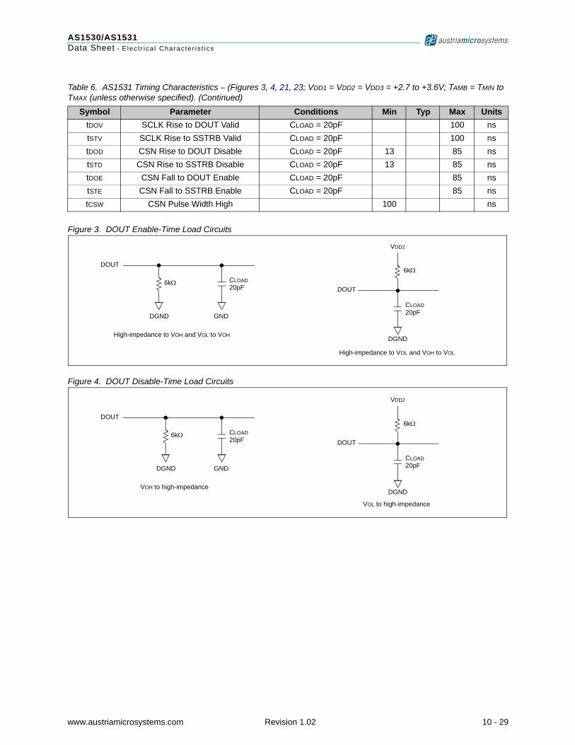
Table 6. AS1531 Timing Characteristics – (Figures 3, 4, 21, 23; VDD1 = VDD2 = VDD3 = +2.7 to +3.6V; TAMB = TMIN to TMAX (unless otherwise specified).
Symbol Parameter Conditions Min Typ Max UnitstCP SCLK Period 208 ns tCH SCLK Pulse Width High 83 ns tCL SCLK Pulse Width Low 83 ns tDS DIN to SCLK Setup 45 ns tDH DIN to SCLK Hold 0 ns tCSS CSN Fall to SCLK Rise Setup 45 ns tCS0 SCLK Rise to CSN Fall ignore 45 ns tDOH SCLK Rise to DOUT Hold CLOAD = 20pF 13 20 ns tSTH SCLK Rise to SSTRB Hold CLOAD = 20pF 13 20 ns
www.austriamicrosystems.com Revision 1.02 9 - 29
AS1530/AS1531Data Sheet - E lec t r i ca l Charac te r i s t i cs
Figure 3. DOUT Enable-Time Load Circuits
Figure 4. DOUT Disable-Time Load Circuits
tDOV SCLK Rise to DOUT Valid CLOAD = 20pF 100 nstSTV SCLK Rise to SSTRB Valid CLOAD = 20pF 100 nstDOD CSN Rise to DOUT Disable CLOAD = 20pF 13 85 nstSTD CSN Rise to SSTRB Disable CLOAD = 20pF 13 85 nstDOE CSN Fall to DOUT Enable CLOAD = 20pF 85 nstSTE CSN Fall to SSTRB Enable CLOAD = 20pF 85 nstCSW CSN Pulse Width High 100 ns
Table 6. AS1531 Timing Characteristics – (Figures 3, 4, 21, 23; VDD1 = VDD2 = VDD3 = +2.7 to +3.6V; TAMB = TMIN to TMAX (unless otherwise specified). (Continued)
Symbol Parameter Conditions Min Typ Max Units
CLOAD 20pF
CLOAD 20pF
6kΩ
GND
DGND
DOUT
DOUT
High-impedance to VOH and VOL to VOH
VDD2
High-impedance to VOL and VOH to VOL
6kΩ
DGND
6kΩ CLOAD 20pF
CLOAD 20pF
6kΩ
DGND GND
DGND
DOUT
DOUT
VOH to high-impedance
VDD2
VOL to high-impedance
www.austriamicrosystems.com Revision 1.02 10 - 29

AS1530/AS1531Data Sheet - Typ ica l Opera t ing Charac te r i s t i cs
www.austriamicrosystems.com Revision 1.02 11 - 29
7 Typical Operating CharacteristicsSame conditions as stated in Electrical Characteristics on page 5.
Figure 5. INL vs. Digital Output Code Figure 6. DNL vs. Digital Output Code
Figure 7. FFT @ 10kHz; RANGE = 1, MODE = 1 Figure 8. FFT @ 75kHz; RANGE = 0, MODE = 1
Figure 9. ENOB vs. VREF; 1st Order 300kHz Figure 10. ENOB vs. Input Signal Frequency; 1st Low Pass Filter Order 1MHz Low Pass Filter
-1
-0.8
-0.6
-0.4
-0.2
0
0.2
0.4
0.6
0.8
1
0 1000 2000 3000 4000Digital Output Code
INL
(LSB
) .
-1
-0.8
-0.6
-0.4
-0.2
0
0.2
0.4
0.6
0.8
1
0 1000 2000 3000 4000Digital Output Code
DN
L (L
SB)
.
-180
-160
-140
-120
-100
-80
-60
-40
-20
0
20
0 20 40 60 80 100 120 140 160
Input Signal Frequency (kHz)
FFT
(dB
C)
e
-180
-160
-140
-120
-100
-80
-60
-40
-20
0
20
0 20 40 60 80 100 120 140 160
Input Signal Frequency (kHz)
FFT
(dB
C)
e
FSample = 312.5kspsNFFT = 16384
FSample = 312.5kspsNFFT = 16384
10.6
10.8
11
11.2
11.4
11.6
1 2 3 4 5Voltage (V)
ENO
B (B
it)
.
AS1531: fsig = 75kHz
AS1530: fsig = 100kHz
11.05
11.1
11.15
11.2
11.25
11.3
11.35
11.4
11.45
11.5
0 50 100 150 200 250 300 350Frequency (kHz)
ENO
B (B
it)
.

AS1530/AS1531Data Sheet - Typ ica l Opera t ing Charac te r i s t i cs
Figure 11. IVDD vs. VDD (Static) Figure 12. IVDD vs. Temperature; Internal Reference
Figure 13. IVDD vs. VDD (Converting) Figure 14. IVDD vs. Temperature (Static)
Figure 15. VREF vs. Temperature
2.5
2.75
3
3.25
3.5
3.75
4
-40 -15 10 35 60 85
Temperature (°C)
Sup
ply
Cur
rent
(mA
) e
AS1530
AS1531
0
0.5
1
1.5
2
2.5
3
3.5
4
2.7 3.05 3.4 3.75 4.1 4.45 4.8 5.15 5.5
Supply Voltage (V)
Sup
ply
Cur
rent
(mA
) e
Internal Reference
External Reference
0
0.5
1
1.5
2
-40 -15 10 35 60 85
Temperature (°C)
Sup
ply
Cur
rent
(mA)
AS1530, Reduced Power Mode, Internal Ref.
AS1531, Reduced Power Mode, Internal Ref.
AS1530, Reduced Power Mode, External Ref.
AS1531, Reduced Power Mode, External Ref.
0
0.5
1
1.5
2
2.5
3
2.7 3.05 3.4 3.75 4.1 4.45 4.8 5.15 5.5
Supply Voltage (V)
Sup
ply
Cur
rent
(mA
) e
Normal Operation; Internal Reference
Reduced Power Mode; Internal Reference
Reduced Power Mode; External Reference
2.49
2.495
2.5
2.505
2.51
-40 -15 10 35 60 85Temperature (°C)
Ref
eren
ce V
olta
ge (V
) .
www.austriamicrosystems.com Revision 1.02 12 - 29

AS1530/AS1531Data Sheet - Typ ica l Opera t ing Charac te r i s t i cs
Figure 16. Offset Error vs. Temperature Figure 17. Offset Error vs. VDD
Figure 18. Gain Error vs. Temperature Figure 19. Gain Error vs. VDD
-1.8
-1.6
-1.4
-1.2
-1
-40 -15 10 35 60 85Temperature (°C)
Offs
et E
rror
(LS
B)
.
-1.8
-1.6
-1.4
-1.2
-1
2.7 3.4 4.1 4.8 5.5
Supply Voltage (V)
Offs
et E
rror
(LS
B)
.
0
1
2
3
4
5
-40 -15 10 35 60 85
Temperature (°C)
Gai
n E
rror (
LSB
) e
-3
-2
-1
0
1
2
3
2.7 3.1 3.5 3.9 4.3 4.7 5.1 5.5
VDD (V)
Gai
n E
rror (
LSB
) e
www.austriamicrosystems.com Revision 1.02 13 - 29

AS1530/AS1531Data Sheet - De ta i led Descr ip t ion
8 Detailed DescriptionAnalog InputThe equivalent input circuit (Figure 20) shows the input architecture: track/hold circuitry, input multiplexer, input com-parator, switched-capacitor DAC, and internal reference. A flexible serial interface provides easy connections to vari-ous microprocessors.
Figure 20. Equivalent Input Circuit
The input tracking circuitry has a 6MHz small-signal bandwidth, thus it is possible to under-sample (digitize high-speed transient events) and measure periodic signals modulated at frequencies exceeding the AS1530/AS1531 sampling rate.
Note: To avoid high-frequency signals being aliased into the frequency band of interest, antialias filtering is recom-mended
Input ProtectionInternal protection diodes (which clamp the analog input to VDD1 and GND) allow the channel inputs to swing from (GND to 0.3V) to (VDD1 + 0.3V) without damaging the devices. However, for accurate conversions near full scale, the inputs must not exceed VDD1 by more than 50mV or be lower than GND by 50mV.
Note: If the analog input exceeds 50mV beyond the supply voltage, do not allow the input current to exceed 2mA.
Track/HoldThe track/hold stage enters tracking mode on the rising edge of SCLK which clocks in bit MODE of the 8-bit control byte (see Figure 21 on page 17). The track/hold stage enters hold mode on the falling clock edge after bit PD0 of the 8-bit control byte has been shifted in.
The time required for the track/hold circuit to acquire an input signal is a function of how quickly the input capacitance is charged. If the input signal source impedance is high, the acquisition time lengthens. The acquisition time (tACQ) is the maximum time the device takes to acquire the signal and is also the minimum time needed for the signal to be acquired.
tACQ is never less than 390ns (AS1530) or 520ns (AS1531), and is calculated by:
tACQ = 9(RS + RIN)18pF (EQ 1)
Where::RIN = 800ΩRS = the source impedance of the input signal.
Note: Source impedances below 2kΩ do not significantly affect the AC performance of the devices.
+
–
+
Comparator
RIN
CSWITCH11pF
CHOLD13pF
–
CH0CH1CH2CH3CH4CH5CH6CH7COM
REF
AIN+
CSWITCH11pF
+
CHOLD13pF
–
SampleSwitch
CSWITCH includes all parasitics
Analog InputMultiplexer
AIN-
www.austriamicrosystems.com Revision 1.02 14 - 29

AS1530/AS1531Data Sheet - De ta i led Descr ip t ion
Control RegisterThe control register on the AS1530/AS1531 is a 8-bit, write-only register. Data is written to this register using the CSN, DIN and SCLK pins. The control register format is shown in Table 7 and the function of the bits are defined in Table 8.
The AS1530/AS1531 operating modes are selected by sending an 8-bit data word to the internal shift register via pin DIN. After pin CSN is pulled low, the first logic 1 on pin DIN is interpreted as a start bit. A start bit is defined as one of the following:! The first logic 1 bit clocked into pin DIN (with CSN low) any time the AS1530/AS1531 is idle, e.g., after VDD1 and
VDD2 are applied.! The first logic 1 bit clocked into pin DIN after bit 6 of a conversion in progress is clocked out of pin DOUT.
Figure 22 on page 17 shows the serial-interface timing necessary to perform a conversion every 16 SCLK cycles. If CSN is tied low and SCLK is continuous, guarantee a start bit by first clocking in sixteen 0s. The fastest speed at which the devices can operate is 16 clocks per conversion (with CSN held low between conversions).
Analog Input Configuration
Table 7. Control Byte Format
Bit 7 Bit 6 Bit 5 Bit 4 Bit 3 Bit 2 Bit 1 Bit 0 START (MSB) SEL2 SEL1 SEL0 RANGE MODE PD1 PD0 (LSB)
Table 8. Bit Descriptions
Bit Name Description 7 START The first logic 1 bit after CSN goes low signifies the start of a control byte.
6:4 SEL2:SEL0 These three bits select which of the eight channels and pin COM are used for the conversion (see Table 10 and Table 11).
3 RANGE This bit selects the analog input range of the AS1530/AS1531.0 = The analog input range extends from -VREF/2 to +VREF/2.1= The analog input range extends from 0V to VREF.
2 MODE
This bit in conjunction with bit RANGE changes the analog input configuration. 0 = The voltage difference between two selectable channels is converted. This setting selects two's complement coding (see Table 10 on page 16 and Table 11 on page 16).1 = One of the eight input channels is referenced to COM. This setting also selects binary coding.
1:0 PD1:PD0
Selects the AS1530/AS1531 operating mode:PD1 PD0 Mode 0 0 Full power-down mode.0 1 Reduced-power mode.1 0 Reduced-power mode.1 1 Normal operation.
Table 9. Analog Input Configuration
Analog Input Configuration Mode Range Coding Comments
8-Channel Single-Ended 1 1 Binary AIN+ from 0 to VREF. COM should be tied to GND.
8-Channel Pseudo Differential referenced to COM 1 1 Binary AIN+ from COM to COM + VREF
8-Channel Pseudo Differential referenced to COM 1 0 Binary AIN+ from -VREF/2+COM to + VREF/2+COM
4-Channel Pseudo Differential 0 1 Two's Complement AIN+ - AIN- from 0 to VREF
4-Channel Pseudo Differential 0 0 Two's Complement AIN+ - AIN- from -VREF/2 to +VREF/2
4-Channel Fully Differential 0 0 Two's Complement AIN+ - AIN- from -VREF/2 to +VREF/2, fully differential input signal.
www.austriamicrosystems.com Revision 1.02 15 - 29

AS1530/AS1531Data Sheet - De ta i led Descr ip t ion
Channel SelectionDepending on the setting of bit MODE (page 15), the internal inputs of the ADC (AIN+ and AIN-) are connected differ-ently to the input channels (CH0:CH7 and COM).
Single-Ended Input
Note: In single-ended mode pin COM should be connected to GND pin.
Differential Input
Table 10. Input Channel Selection for MODE = 1
SEL2 SEL1 SEL0 CH0 CH1 CH2 CH3 CH4 CH5 CH6 CH7 COM 0 0 0 AIN+ AIN-
0 0 1 AIN+ AIN-
0 1 0 AIN+ AIN-
0 1 1 AIN+ AIN-
1 0 0 AIN+ AIN-
1 0 1 AIN+ AIN-
1 1 0 AIN+ AIN-
1 1 1 AIN+ AIN-
Table 11. Input Channel Selection for MODE = 0
SEL2 SEL1 SEL0 CH0 CH1 CH2 CH3 CH4 CH5 CH6 CH7 0 0 0 AIN+ AIN-
0 0 1 AIN+ AIN-
0 1 0 AIN+ AIN-
0 1 1 AIN+ AIN-
1 0 0 AIN- AIN+
1 0 1 AIN- AIN+
1 1 0 AIN- AIN+
1 1 1 AIN- AIN+
www.austriamicrosystems.com Revision 1.02 16 - 29

AS1530/AS1531Data Sheet - De ta i led Descr ip t ion
Starting a ConversionA conversion is started by clocking a control byte into pin DIN.
With CSN low, each rising edge on SCLK clocks a bit from DIN into the internal shift register, starting with the MSB. A conversion will only start when a logic 1 is written to the START bit of the 8-bit control register.
Figure 21. Single Conversion Timing Waveforms
Figure 22. Continuous 16-Clock Conversion Timing Waveforms
RANGE
B11 B10 B9 B8 B7 B0B1B2B3B4B5B6
tACQ
RB1 RB2 RB3
Single ConversionAcquireIdle Idle
1 4 8 9 12 2016 24
Start
High-Z High-Z
High-Z High-Z
CSN
SCLK
DIN
SSTRB
DOUT
SEL2 SEL1 SEL0 MODE PD0PD1
High-Z
CSN
DIN
SSTRB
SCLK
B11 B11B0 B6B6 B6B0
...
Conversion Result 0 Conversion Result 1
Control Byte 0 Control Byte 1 Control Byte 2
High-ZB11
1 128 16 1 128 161 128 16
S S S S
DOUTConversion Result 2
www.austriamicrosystems.com Revision 1.02 17 - 29

AS1530/AS1531Data Sheet - De ta i led Descr ip t ion
Figure 23. Detailed Serial Interface Timing Waveforms
The external serial clock shifts data in and out of the devices and drives the analog-to-digital conversion steps. Two clock periods after the last bit of the control byte is written the output pin SSTRB pulses high for one clock period.
The serial data is shifted out at DOUT on each of the next 12 SCLK rising edges (see Figure 21 on page 17).
Pins SSTRB and DOUT go into a high-impedance state when CSN goes high. The conversion must complete in 120µs or less, or consequently, droop on the sample-and-hold capacitors may degrade conversion results. Figure 23 shows detailed serial-interface timing waveforms.
Transfer FunctionsOutput coding and transfer function depend on the control register bits MODE (page 15) and RANGE (page 15).
Figure 24. Straight Binary Transfer Function for Figure 25. Straight Binary Transfer Function forRANGE = 1 and MODE = 1 RANGE = 0 and MODE = 1
tDH
CSN
SCLK
DIN
SSTRB
DOUT
tCSS tCP tCSWtCSO
tCL tCH
tDOH
tDOVtDOD
tSTD
tSTH
tDS
tDOE
tSTE tSTV
11...111
11...1110
11....101
00...011
00...010
00...001
00...000
Out
put C
ode
0 1 2 3Input Voltage AIN+ - AIN- (LSB)
FS - 3/2LSB
Full Scale (FS) Transition
Full Scale = VREFZero Scale = 01LSB = VREF/4096
11...111
11...1110
11....101
00...011
00...010
00...001
00...000
Out
put C
ode
ZS ZS+1LSBInput Voltage AIN+ - AIN- (LSB)
FS - 3/2LSB
Full Scale (FS) Transition
Full Scale = +VREF/2Zero Scale = -VREF/21LSB = VREF/4096
www.austriamicrosystems.com Revision 1.02 18 - 29

AS1530/AS1531Data Sheet - De ta i led Descr ip t ion
Figure 26. Two’s Complement Transfer Function for Figure 27. Two’s Complement Transfer Function forRANGE = 1 and MODE = 0 RANGE = 0 and MODE = 0
Power ModesPower consumption can be reduced by placing the AS1530/AS1531 in reduced power mode or in full power-down mode between conversions.
The power mode is selected using bits PD1 and PD0 of the 8-bit control byte.
Table 12 lists the three operating modes with the corresponding supply current and active device circuits. For data rates achievable in full power-down mode see Full Power-Down Mode on page 20.
* Circuit operation between conversions; during conversion all circuits are fully powered up.
The selected power-down mode (as shown in Table 12) is initiated after an analog-to-digital conversion is completed.
In all power modes the serial interface remains active, waiting for a new control byte to start conversion (see Figure 30 on page 21). Once the conversion is completed, the AS1530/AS1531 goes into the selected power mode until a new control byte is shifted in. In reduced power mode the AS1530/AS1531 will be able to start conversion immediately when running at decreased clock rates. In full power down mode wait until the internal reference has stabilized (depen-dant on the values of the capacitance of REF and REFADJ).
During initialization the AS1530/AS1531 immediately go into normal operation mode and are ready to convert after 4µs when using an external reference. When using the internal reference, wait until the internal reference has stabilized (dependant on the values of the capacitance of REF and REFADJ).
Table 12. Software Controlled Power Modes
PD1/PD0(page 23) Mode
Total Supply Current Device Circuits *
During Conversion After Conversion Input Comparator Reference
AS1530 AS1531 AS1530 AS153100 Full Power-Down Mode 2.8mA 2.2mA 0.5µA 0.5µA Off Off 01
Reduced-Power Mode 2.8mA 2.2mA 0.4mA 0.4mA Reduced Power On
10 11 Normal Operation 2.8mA 2.2mA 2.0mA 1.8mA Full Power On
011....111
011...110
000...010
000...001
000...000
111...111
111...110
111...101
100...001
100...000
Out
put C
ode
-FS ZSInput Voltage AIN+ - AIN- (LSB)
+FS - 1LSB
Full Scale = VREF-Full Scale = 0Zero Scale = VREF/21LSB = VREF/4096
011....111
011...110
000...010
000...001
000...000
111...111
111...110
111...101
100...001
100...000
Out
put C
ode
-FS ZSInput Voltage AIN+ - AIN- (LSB)
+FS - 1LSB
Full Scale = +VREF/2-Full Scale = -VREF/2Zero Scale = 01LSB = VREF/4096
www.austriamicrosystems.com Revision 1.02 19 - 29

AS1530/AS1531Data Sheet - De ta i led Descr ip t ion
Reduced Power ModeReduced power mode is activated using bits PD1 and PD0 (see Table 12). When reduced power mode is asserted, the AS1530/AS1531 completes any conversion in progress and enters reduced power mode.
The next start of conversion puts the AS1530/AS1531 into normal operation mode. The 8-bit control byte shifted into the control register determines the next power mode. For example, if the 8-bit control byte contains PD1 = 0 and PD0 = 1, reduced power mode starts immediately after the conversion (see Figure 28).
The reduced-power mode achieves the lowest power consumption at speeds close to the maximum sample rate. Figure 29 shows the AS1531 power consumption in reduced-power mode and normal operating mode (see Table 12 on page 19) with the internal reference and maximum clock speed.
Figure 28. Reduced-Power Mode Timing Waveforms (AS1531)
Note: The clock speed in reduced-power mode should be limited to 4.8MHz. Full power-down mode may provide increased power savings in applications where the devices are inactive for long periods of time, where intermit-tent bursts of high-speed conversions are required.
Figure 29. Normal Operation and Reduced Power Mode using Internal Reference (AS1531)
Full Power-Down ModeFull power-down is activated using bits PD1 and PD0 (see Table 12). Full power-down mode offers the lowest power consumption at up to 1000 conversions per-channel per-second. When full power-down is asserted, the AS1530/AS1531 completes any conversion in progress and powers down into specified low-quiescent current state.
The start of the next conversion puts the AS1530/AS1531 into normal operation mode. The 8-bit control byte shifted into the control register determines the next power mode. For example, if the 8-bit control byte contains PD1 = 0 and PD0 = 0, full power-down mode starts immediately after the conversion (see Figure 30 on page 21)
DIN 1
VDD1+VDD2+VDD3
1 1 1 1 10 0 0
Reduced-Power Mode
Reduced-Power Mode
Reduced-Power Mode
2.50V (Always On)
2.2mA 2.2mA 2.2mA
0.4mA 0.4mA 0.4mA
REF
Normal ModeConversion
Reduced Power Mode
Normal ModeConversion
Reduced Power Mode
Normal ModeConversion
Reduced Power Mode
0
500
1000
1500
2000
2500
3000
0.001 0.1 10 1000Sampling Rate (ksps)
Supp
ly C
urre
nt (µ
A) .
Reduced Power Mode
Normal Operation
www.austriamicrosystems.com Revision 1.02 20 - 29

AS1530/AS1531Data Sheet - De ta i led Descr ip t ion
A 0.01µF bypass capacitor plus the internal 17kΩ reference resistor at REFADJ form an R/C filter with a 170µs time constant. To achieve full 12-bit accuracy, 9 time constants (1.8ms) are required after power-up if the bypass capacitor is fully discharged between conversions. Waiting this 1.8ms in reduced-power mode instead of normal operation mode can further reduce power consumption. This is achieved by using the sequence shown in Figure 30 on page 21.
Figure 31 on page 21 shows the AS1531 power consumption for conversions using full power-down mode (PD1 = PD0 = 0 (see Table 12), an external reference, and the maximum clock speed. One dummy conversion to power-up the device is required, but no wait-time is necessary to start the second conversion, thereby achieving lower power con-sumption up to the full sampling rate.
Figure 30. Full Power-Down Timing Waveforms (AS1531)
Figure 31. Average Supply Current vs. Sampling Rate (AS1531, FULLPD, and External Reference)
ReferenceThe AS1530/AS1531 can operate with the internal or an external reference.
Internal ReferenceThe internal reference is selected by placing a capacitor between REFADJ and GND. The internally trimmed 1.22V bandgap voltage available at REFADJ is buffered with a gain of 2.045V/V to pin REF, where 2.5V are available. A decoupling capacitor is needed at pin REF.
DIN1 0 1 1 1 00 0 0
Full Power-Down
Reduced-Power Mode
REF
1
REFADJ
IVDD1+IVDD2+IVDD3
Full Power-Down
1.22V
2.5V
2.2mA 2.2mA 2.2mA
2.5V
1.22V
0mA 0mA0.4mA
γ = R/C = 17Ωk x 0.01µF
Full Power-Down
Normal ModeConversion
Normal ModeDummy
ConversionReduced
Power Mode
Normal ModeConversion
Full Power-Down
1 Channel
0.1
100
100000
0.001 0.01 0.1 1 10 100Sampling Rate (ksps)
Supp
ly C
urre
nt (µ
A) .
www.austriamicrosystems.com Revision 1.02 21 - 29

AS1530/AS1531Data Sheet - De ta i led Descr ip t ion
Additionally the bandgap voltage can be adjusted about ±100mV by forcing a voltage to the REFADJ pin. The REFADJ input impedance is typically 17kΩ. Figure 32 shows a possible arrangement.
Figure 32. Reference Adjust Circuit
External ReferenceAn external reference can be connected directly at pin REF. To use the external reference, the internal buffer must be disabled by connecting pin REFADJ to pin VDD. The input resistance is typically 15kΩ.
During conversion, an external reference at pin REF must deliver up to 350µA DC load current and have 10Ω or less output impedance. If the reference has a higher output impedance or is noisy, bypass it with a 4.7µF capacitor placed as close to pin REF as possible.
Note: Using the REFADJ input makes buffering the external reference unnecessary.
CLOAD 0.01µF
GND
100kΩ
DGND
24kΩ
510kΩ
+3.3V
12REFADJ
AS1530/AS1531
www.austriamicrosystems.com Revision 1.02 22 - 29

AS1530/AS1531Data Sheet - App l ica t ion In fo rmat ion
9 Application InformationInitializationWhen power is first applied to the AS1530/AS1531 internal power-on reset circuitry sets the devices for normal opera-tion. At this point, the devices can perform data conversions with CSN held low.
Note: The device requires 10µs after the power supplies stabilize; no conversions should be initiated during this time.
The digital output at pin DOUT will be all 0s until an analog-to-digital conversion is initiated.
Serial InterfaceThe AS1530/AS1531 fully support SPI, QSPI, and Microwire interfaces. For SPI, select the correct clock polarity and sampling edge in the SPI control registers (set CPOL = 0 and CPHA = 0).
Note: Microwire, SPI, and QSPI all transmit a byte and receive a byte at the same time.
Using the circuit shown in Figure 33 on page 24, the simplest software interface requires only three 8-bit transfers to perform a conversion (one 8-bit transfer to configure the AS1530/AS1531, and two more 8-bit transfers to clock out the 12-bit conversion result).
Serial Interface ConfigurationThe following steps describe how to configure the serial interface:
1. Confirm that the CPU serial interface is in master mode (so the CPU generates the serial clock). 2. Choose a clock frequency from 500kHz to 6.4MHz (AS1530) or 4.8MHz (AS1531).3. Set up the control byte and call it TB1. TB1 should be in the format 1XXXXXXX binary, where the Xs indicate the
selected channel, conversion mode, and power mode.4. Use a general-purpose I/O line on the CPU to pull CSN low. 5. Transmit TB1 and simultaneously receive a byte (RB1). Ignore this byte.6. Transmit a byte of all zeros ($00h) and simultaneously receive byte RB2.7. Transmit a byte of all zeros ($00h) and simultaneously receive byte RB3.8. Pull CSN high.
Bytes RB2 and RB3 (see Figure 21 on page 17) contain the results of the conversion, padded with three leading zeros and one trailing zero. The total conversion time is a function of the serial-clock frequency and the amount of idle time between 8-bit transfers. To avoid excessive track/hold droop, make sure the total conversion time does not exceed 120µs.
www.austriamicrosystems.com Revision 1.02 23 - 29

AS1530/AS1531Data Sheet - App l ica t ion In fo rmat ion
Figure 33. Operational Diagram
QSPI InterfaceThe AS1530/AS1531 can interface with QSPI using the circuit in Figure 34 (fSCLK = 4.0MHz, CPOL = 0, CPHA = 0). This QSPI circuit can be programmed to do a conversion on each of the eight channels. The result is stored in memory without affecting CPU performance, since QSPI incorporates a micro-sequencer.
Figure 34. QSPI Interface Connections
+2.5VAnalogInputs
0.1µF
12REFADJ
20VDD1
4.7µF
1CH0
19VDD2
13GND
17CSN
14DOUT15SSTRB
CPU
VDD
I/O18SCLK16DIN
SCK (SK)
MOSI (SO)
MISO (SI)
VSS
0.1µF
+3 to +5V
11REF
AS1530/AS1531
10VDD3
.
.
.
8CH7
9COM
10µF
+2.5VAnalogInputs
0.1µF
12REFADJ
11REF
4.7µF
1CH0
8CH7
13GND
14DOUT15SSTRB
CPUPCSO
SCK
MOSI
MISO GND
0.1µF
17CSN
16DIN
18SCLK
+10µF
Power Supplies
+3 or +5V
+3 or +5V
AS1530/AS1531
20VDD1
19VDD2
10VDD3
.
.
.
9COM
www.austriamicrosystems.com Revision 1.02 24 - 29

AS1530/AS1531Data Sheet - App l ica t ion In fo rmat ion
Quick Evaluation CircuitIn order to quickly evaluate the analog performance of the AS1530/AS1531, use the circuit shown in Figure 35.
Figure 35. Evaluation Circuit Diagram
Connecting DIN to VDD2 shifts in control bytes of $FFh, which trigger single-ended conversions (bit RANGE (page 15) = 1) on CH7 without powering down between conversions. The SSTRB output pulses high for one clock period before the MSB of the 12-bit conversion result is shifted out of DOUT. Varying the analog input to CH7 will alter the sequence of bits from DOUT. A total of 16 clock cycles is required per conversion.
Note: All SSTRB and DOUT output transitions occur 25ns (typ) after the rising edge of SCLK.
+2.5VAnalog
Input
0.1µF
12REFADJ
11REF
4.7µF
13GND
17CSN
14DOUT15SSTRB
18SCLK16DIN
0.1µF
To VDD2
0.1µF 10µF
+3 or +5V
External Clock
8CH7
AS1530/AS1531
TBA
20VDD1
19VDD210VDD3
9COM
www.austriamicrosystems.com Revision 1.02 25 - 29

AS1530/AS1531Data Sheet - App l ica t ion In fo rmat ion
Layout ConsiderationsThe AS1530/AS1531 require proper layout and design procedures for optimum performance.
! Use printed circuit boards; wirewrap boards should not be used.
! Analog and digital traces should be separate and should not run parallel to each other (especially clock traces).
! Digital traces should not run beneath the AS1530/AS1531.
! Use a single-point analog ground at GND, separate from the digital ground (see Figure 36). Connect all other ana-log grounds and DGND to this star ground point for further noise reduction. No other digital system ground should be connected to this single-point analog ground. The ground return to the power supply for this ground should be low impedance and as short as possible for noise-free operation.
! High-frequency noise in the VDD power supply may affect the AS1530/AS1531 high-speed comparator. Bypass this supply to the single-point analog ground with 0.1µF and 4.7µF bypass capacitors. Bypass capacitors should be as close to the device as possible for optimum power supply noise-rejection. If the power supply is very noisy, a 10Ω resistor can be connected as a low-pass filter to attenuate supply noise (see Figure 36).
Figure 36. Recommended GND Design
Power Supplies
DigitalCircuitry
+
+
10Ω(Optional)
9COM
VDD1
GND
GND
VDD2
DGND
VDD
19VDD2
13GND
20VDD1
AS1530/AS1531
10VDD3
www.austriamicrosystems.com Revision 1.02 26 - 29

AS1530/AS1531Data Sheet - Package Drawings and Mark ings
10 Package Drawings and MarkingsFigure 37. 20-pin TSSOP Package
Symbol Min Typ Max NotesA - - 1.10 1,2
A1 0.05 - 0.15 1,2A2 0.85 0.90 0.95 1,2L 0.50 0.60 0.75 1,2R 0.09 - - 1,2
R1 0.09 - - 1,2b 0.19 - 0.30 1,2,5
b1 0.19 0.22 0.25 1,2c 0.09 - 0.20 1,2c1 0.09 - 0.16 1,2θ1 0º - 8º 1,2L1 1.0REF 1,2aaa 0.10 1,2bbb 0.10 1,2ccc 0.05 1,2ddd 0.20 1,2e 0.65BSC 1,2
θ2 12ºREF 1,2θ3 12ºREF 1,2
VariationsD 6.40 6.50 6.60 1,2,3,8E1 4.30 4.40 4.50 1,2,4,8E 6.4BSC 1,2e 0.65BSC 1,2N 20 1,2,6
Notes:1. All dimensions are in millimeters; angles in degrees.2. Dimensioning and tolerancing per ASME Y14.5M – 1994.3. Dimension D does not include mold flash, protrusions, or gate
burrs. Mold flash, protrusions, and gate burrs shall not exceed 0.15mm per side.
4. Dimension E1 does not include interlead flash or protrusion. Interlead flash or protrusions shall not exceed 0.25mm per side.
5. Dimension b does not include dambar protrusion. Allowable dambar protrusion shall be 0.08mm total in excess of the b dimension at maximum material condition. Dambar cannot be located on the lower radius of the foot.
6. Terminal numbers are for reference only.7. Datums A and B to be determined at datum plane H.8. Dimensions D and E1 are to be determined at datum plane H.9. This dimension applies only to variations with an even number
of leads per side.10. Cross section A-A to be determined at 0.10 to 0.25mm from
the leadtip.
www.austriamicrosystems.com Revision 1.02 27 - 29

AS1530/AS1531Data Sheet - Order ing In format ion
11 Ordering InformationThe devices are available as the standard products shown in Table 13.
Table 13. Ordering Information
Model Description Delivery Form PackageAS1530-T 12-bit ADC, 8-channel, 400ksps Tape and Reel 20-pin TSSOP
AS1530 12-bit ADC, 8-channel, 400ksps Tubes 20-pin TSSOP
AS1531-T 12-bit ADC, 8-channel, 300ksps Tape and Reel 20-pin TSSOP
AS1531 12-bit ADC, 8-channel, 300ksps Tubes 20-pin TSSOP
www.austriamicrosystems.com Revision 1.02 28 - 29

AS1530/AS1531Data Sheet
CopyrightsCopyright © 1997-2007, austriamicrosystems AG, Schloss Premstaetten, 8141 Unterpremstaetten, Austria-Europe. Trademarks Registered ®. All rights reserved. The material herein may not be reproduced, adapted, merged, translated, stored, or used without the prior written consent of the copyright owner.
All products and companies mentioned are trademarks or registered trademarks of their respective companies.
DisclaimerDevices sold by austriamicrosystems AG are covered by the warranty and patent indemnification provisions appearing in its Term of Sale. austriamicrosystems AG makes no warranty, express, statutory, implied, or by description regarding the information set forth herein or regarding the freedom of the described devices from patent infringement. austriamicrosystems AG reserves the right to change specifications and prices at any time and without notice. Therefore, prior to designing this product into a system, it is necessary to check with austriamicrosystems AG for current information. This product is intended for use in normal commercial applications. Applications requiring extended temperature range, unusual environmental requirements, or high reliability applications, such as military, medical life-support or life-sustaining equipment are specifically not recommended without additional processing by austriamicrosystems AG for each application. For shipments of less than 100 parts the manufacturing flow might show deviations from the standard production flow, such as test flow or test location.
The information furnished here by austriamicrosystems AG is believed to be correct and accurate. However, austriamicrosystems AG shall not be liable to recipient or any third party for any damages, including but not limited to personal injury, property damage, loss of profits, loss of use, interruption of business or indirect, special, incidental or consequential damages, of any kind, in connection with or arising out of the furnishing, performance or use of the technical data herein. No obligation or liability to recipient or any third party shall arise or flow out of austriamicrosystems AG rendering of technical or other services.
Contact InformationHeadquartersaustriamicrosystems AGA-8141 Schloss Premstaetten, Austria
Tel: +43 (0) 3136 500 0Fax: +43 (0) 3136 525 01
For Sales Offices, Distributors and Representatives, please visit:
http://www.austriamicrosystems.com/contact
www.austriamicrosystems.com Revision 1.02 29 - 29