
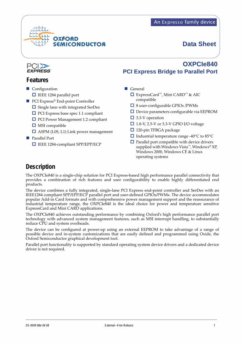
An Expresso family device - SymmetryElectronics.com · DS-0049 Mar 06 08 External—Free Release 1...
40
DS-0049 Mar 06 08 External—Free Release 1 An Expresso family device Configuration IEEE 1284 parallel port PCI Express ® End‐point Controller Single lane with integrated SerDes PCI Express base spec 1.1 compliant PCI Power Management 1.2 compliant MSI compatible ASPM (L0S, L1) Link power management Parallel Port IEEE 1284‐compliant SPP/EPP/ECP General ExpressCard ™ , Mini CARD ™ & AIC compatible 8 user‐configurable GPIOs /PWMs Device parameters configurable via EEPROM 3.3‐V operation 1.8‐V, 2.5‐V or 3.3‐V GPIO I/O voltage 120‐pin TFBGA package Industrial temperature range ‐40°C to 85°C Parallel port compatible with device drivers supplied with Windows Vista ™ , Windows ® XP, Windows 2000, Windows CE & Linux operating systems Data Sheet Features Description The OXPCIe840 is a single‐chip solution for PCI Express‐based high performance parallel connectivity that provides a combination of rich features and user configurability to enable highly differentiated end products. The device combines a fully integrated, single‐lane PCI Express end‐point controller and SerDes with an IEEE1284 compliant SPP/EPP/ECP parallel port and user‐defined GPIOs/PWMs. The device accommodates popular Add‐in Card formats and with comprehensive power management support and the reassurance of industrial temperature range, the OXPCIe840 is the ideal choice for power and temperature sensitive ExpressCard and Mini CARD applications. The OXPCIe840 achieves outstanding performance by combining Oxford’s high performance parallel port technology with advanced system management features, such as MSI interrupt handling, to substantially reduce CPU and system overheads. The device can be configured at power‐up using an external EEPROM to take advantage of a range of possible device and in‐system customizations that are easily defined and programmed using Oxide, the Oxford Semiconductor graphical development tool. Parallel port functionality is supported by standard operating system device drivers and a dedicated device driver is not required. OXPCIe840 PCI Express Bridge to Parallel Port
Transcript of An Expresso family device - SymmetryElectronics.com · DS-0049 Mar 06 08 External—Free Release 1...
DS-0049 Mar 06 08 External—Free Release 1
An Expresso family device
ConfigurationIEEE 1284 parallel port
PCI Express® End‐point ControllerSingle lane with integrated SerDes PCI Express base spec 1.1 compliant PCI Power Management 1.2 compliant MSI compatible ASPM (L0S, L1) Link power management
Parallel PortIEEE 1284‐compliant SPP/EPP/ECP
GeneralExpressCard™, Mini CARD™ & AIC compatible8 user‐configurable GPIOs /PWMsDevice parameters configurable via EEPROM 3.3‐V operation 1.8‐V, 2.5‐V or 3.3‐V GPIO I/O voltage 120‐pin TFBGA package Industrial temperature range ‐40°C to 85°C Parallel port compatible with device drivers supplied with Windows Vista™, Windows® XP, Windows 2000, Windows CE & Linux operating systems
Data Sheet
Features
DescriptionThe OXPCIe840 is a single‐chip solution for PCI Express‐based high performance parallel connectivity that provides a combination of rich features and user configurability to enable highly differentiated end products. The device combines a fully integrated, single‐lane PCI Express end‐point controller and SerDes with an IEEE1284 compliant SPP/EPP/ECP parallel port and user‐defined GPIOs/PWMs. The device accommodates popular Add‐in Card formats and with comprehensive power management support and the reassurance of industrial temperature range, the OXPCIe840 is the ideal choice for power and temperature sensitive ExpressCard and Mini CARD applications.The OXPCIe840 achieves outstanding performance by combining Oxford’s high performance parallel port technology with advanced system management features, such as MSI interrupt handling, to substantially reduce CPU and system overheads. The device can be configured at power‐up using an external EEPROM to take advantage of a range of possible device and in‐system customizations that are easily defined and programmed using Oxide, the Oxford Semiconductor graphical development tool. Parallel port functionality is supported by standard operating system device drivers and a dedicated device driver is not required.
OXPCIe840 PCI Express Bridge to Parallel Port
2 External—Free Release DS-0049 Mar 06 08
Oxford Semiconductor, Inc.
Contents Features 1
Description 1
Contents 2
Device Modes 3
OXPCIe840 Pin Descriptions 5
Configuration Space & Base Address Registers 9OXPCIe840 Configuration Space - - - - - - - - - - - - - - - - 9Base Address Register Allocation - - - - - - - - - - - - - - - -11
System Overview 12OXPCIe840 Clocking and Reset Scheme - - - - - - - - - - - -12Personality Application - - - - - - - - - - - - - - - - - - - - -12Interrupt Management - - - - - - - - - - - - - - - - - - - - - -13PCI Express Interface - - - - - - - - - - - - - - - - - - - - - -14Power Management - - - - - - - - - - - - - - - - - - - - - - -14Power Supply Management - - - - - - - - - - - - - - - - - - -14
OXPCIe840 Functions 15Parallel Port Function - - - - - - - - - - - - - - - - - - - - - -15GPIO Function - - - - - - - - - - - - - - - - - - - - - - - - -18
EEPROM Interface & Programming Capabilities 27Overview - - - - - - - - - - - - - - - - - - - - - - - - - - - -27EEPROM Zone Allocation - - - - - - - - - - - - - - - - - - - -29
Operating Conditions 32Maximum Ratings - - - - - - - - - - - - - - - - - - - - - - - -32Electrical Characteristics - - - - - - - - - - - - - - - - - - - -33AC Electrical Characteristics - - - - - - - - - - - - - - - - - -34
Package Mechanical Drawings 37
Ordering Information 38
Contacting Oxford Semiconductor 38
Revision Information 39

DS-0049 Mar 06 08 External—Free Release 3
Oxford Semiconductor, Inc.
Device Modes
The OXPCIe840 allows one parallel device to be efficiently connected to a PCI Express‐enabled host PC. Note that the OXPCIe840 parallel port is intended for use with standard operating system drivers.
Table 1 shows the PCI Express functions available with the OXPCIe840.
Notes: 1 These functions are driven by standard operating system drivers.2 These functions are driven by Oxford Semiconductor drivers.3 Setting this pin to logic 0 disables the GPIO function.
Table 1 PCI Express Function Usage for the OXPCIe840
GPIO_EN Pin
Function 0 Function 1 Function 2 Function 3
1(3) PPORT(1) not visible GPIO(2) not visible

4 External—Free Release DS-0049 Mar 06 08
Oxford Semiconductor, Inc.
Figure 1 shows the OXPCIe840 architecture.
Figure 1 OXPCIe840 Block Diagram
PCI Express PHY
PCI Express Endpoint Controller
Downstream Bridge
Upstream Bridge
GPIO
EEPROM Controller
Interrupt Controller
EEPROM Interface
GPIO[7:0]
Configuration&
Clock/ResetControl
Power Management
PCI Express PHY
Interface
PCI Express Control
Interface
Parallel Port Controller
Parallel Port
Interface

DS-0049 Mar 06 08 External—Free Release 5
Oxford Semiconductor, Inc.
OXPCIe840 Pin Descriptions
Table 2 lists the OXPCIe840 pins and descriptions.
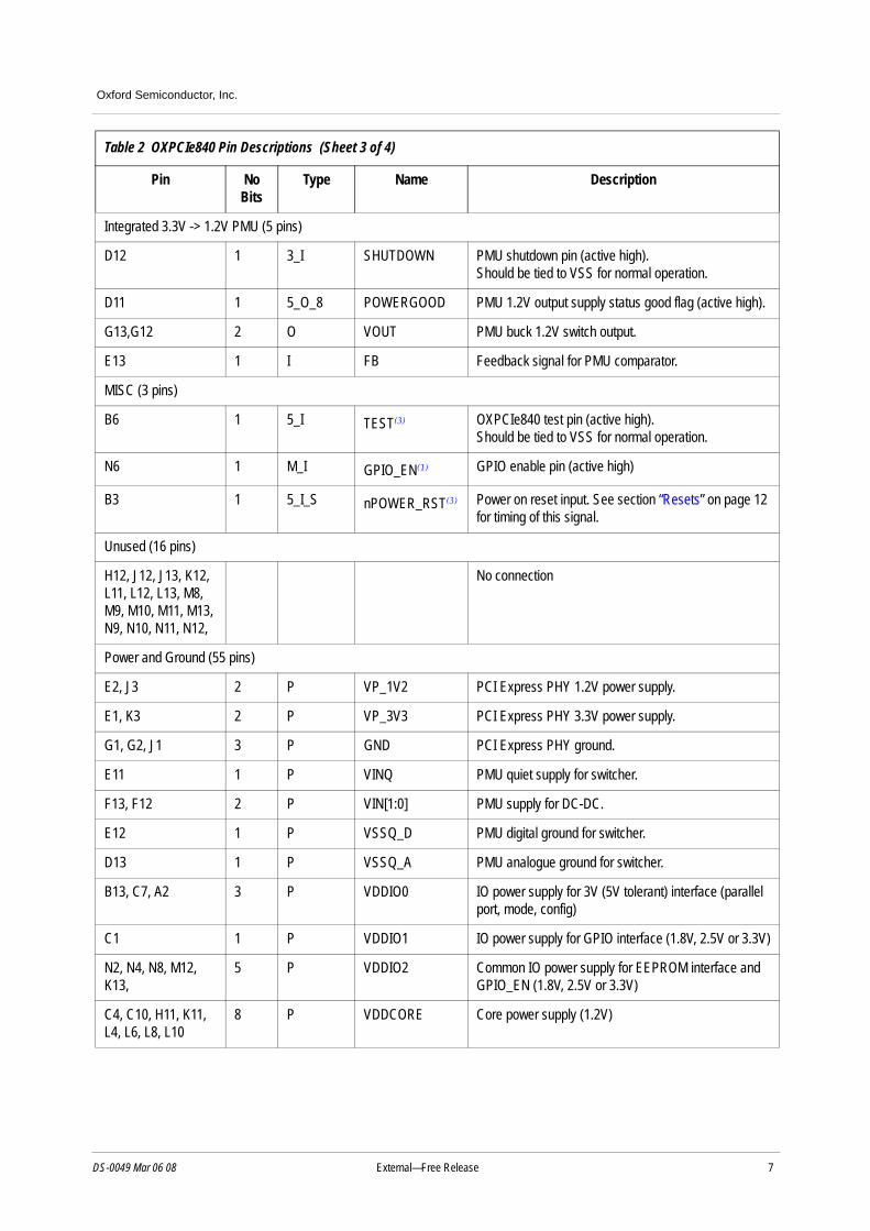
Table 2 OXPCIe840 Pin Descriptions (Sheet 1 of 4)
Pin No Bits
Type Name Description
Microwire™ EEPROM (4 pins)(1)
M4 1 M_O_6 EECK EEPROM serial clock (745 kHz).
M3 1 M_O_6 EECS EEPROM chip select (active high).
N3 1 M_I_6 EEDI EEPROM data in.
N5 1 M_O_6 EEDO EEPROM data out.
GPIO (8 pins)(2)
D1, D2, D3, C2,B1, A1, B2, C3
8 M_B_6 GPIO_[7:0] General Purpose IO.
PCI Express Control (3 pins)(3)
A4 1 5_O_T nWAKE PCI Express edge connector wake (WAKE#).
B4 1 5_O_T nCLKREQ PCI Express edge connector clock request (CLKREQ#).
A3 1 5_I_S nPERST PCI Express edge connector reset (PERST#).
Parallel Port (18 pins)(3)
B11,A11,B10,A10, B9, A9,C9,C8
8 5_B_8 P_DATA[7:0] Data bus
C11 1 5_I nERR SPP mode => nFault (active low). Set low by the peripheral to indicate that an error has occurred.
C12 1 5_I SLCT SPP mode => Select (active high). Set high by the peripheral to indicate that the peripheral is online.
C13 1 5_I BUSY SPP mode => Busy (active high). Driven high by the peripheral to indicate that he peripheral is not ready to receive data.EPP mode => nWait (active low). Driven inactive as a positive acknowledgment from the peripheral that transfer of data or address is completed. It should be driven active as an indication that the device is ready for the next address or data transfer.
B12 1 5_I PE SPP mode => PError (active high). Driven high by the peripheral to indicate that the peripheral has encountered an error in its paper path.

6 External—Free Release DS-0049 Mar 06 08
Oxford Semiconductor, Inc.
A12 1 5_I nACK SPP mode => nAck. Pulsed low by the peripheral to acknowledge transfer of the data byte from the host.EPP mode => Intr (active low). Pulsed low by the peripheral to interrupt the host.
B8 1 5_O_8_T
5_O_8
nINIT SPP mode => nInit (active low). Pulsed low in conjunction with IEEE 1284 Active low to reset the interface and force a return to Compatibility Mode idle phase.EPP mode => nInit (active low). When driven low this signal initiates a termination cycle that results in the interface returning to Compatibility Mode.
B7 1 5_O_8_T
5_O_8
nAFD SPP mode => nAutoFd (active low). Set low by the host to put printer into auto line feed mode.EPP mode => nDStrb (active low). Used to denote a data cycle.
A8 1 5_O_8_T
5_O_8
nSTB SPP mode => nStrobe (active low). Set active low to transfer data into the input latch of the peripheral. Data is valid while nStrobe is low.EPP mode => nWrite (active low). Set low to denote an address or data write operation to the peripheral. Set high to denote an address or data read operation from the peripheral.
C6 1 5_O_8_T
5_O_8
nSLIN SPP mode => nSelectIn (active low). Set low by host to select peripheral.EPP mode => nAStrb (active low). Used to denote an address cycle.
A7 1 5_O_8 DIR Line driver bidirectional control.Logic ‘1’ => data is output.Logic ‘0’ => data is input.
PCI Express PHY (8 pins)
K1 1 O TX_P High speed differential transmit line.
K2 1 O TX_N High speed differential transmit line.
H1 1 I RX_P High speed differential receive line.
H2 1 I RX_N High speed differential receive line.
F1 1 I REFCLK_P Differential reference clock input.
F2 1 I REFCLK_N Differential reference clock input.
G3 1 A REXT Reference resistor connection.191Ω 1% 100ppm/deg C precision resistor to ground.
M2 1 A PCIe_TEST PCI Express PHY test pin (active high).Should be tied to VSS for normal operation.
Table 2 OXPCIe840 Pin Descriptions (Sheet 2 of 4)
Pin No Bits
Type Name Description
DS-0049 Mar 06 08 External—Free Release 7
Oxford Semiconductor, Inc.
Integrated 3.3V -> 1.2V PMU (5 pins)
D12 1 3_I SHUTDOWN PMU shutdown pin (active high).Should be tied to VSS for normal operation.
D11 1 5_O_8 POWERGOOD PMU 1.2V output supply status good flag (active high).
G13,G12 2 O VOUT PMU buck 1.2V switch output.
E13 1 I FB Feedback signal for PMU comparator.
MISC (3 pins)
B6 1 5_I TEST(3) OXPCIe840 test pin (active high).Should be tied to VSS for normal operation.
N6 1 M_I GPIO_EN(1) GPIO enable pin (active high)
B3 1 5_I_S nPOWER_RST(3) Power on reset input. See section “Resets” on page 12 for timing of this signal.
Unused (16 pins)
H12, J12, J13, K12, L11, L12, L13, M8, M9, M10, M11, M13, N9, N10, N11, N12,
No connection
Power and Ground (55 pins)
E2, J3 2 P VP_1V2 PCI Express PHY 1.2V power supply.
E1, K3 2 P VP_3V3 PCI Express PHY 3.3V power supply.
G1, G2, J1 3 P GND PCI Express PHY ground.
E11 1 P VINQ PMU quiet supply for switcher.
F13, F12 2 P VIN[1:0] PMU supply for DC-DC.
E12 1 P VSSQ_D PMU digital ground for switcher.
D13 1 P VSSQ_A PMU analogue ground for switcher.
B13, C7, A2 3 P VDDIO0 IO power supply for 3V (5V tolerant) interface (parallel port, mode, config)
C1 1 P VDDIO1 IO power supply for GPIO interface (1.8V, 2.5V or 3.3V)
N2, N4, N8, M12, K13,
5 P VDDIO2 Common IO power supply for EEPROM interface and GPIO_EN (1.8V, 2.5V or 3.3V)
C4, C10, H11, K11,L4, L6, L8, L10
8 P VDDCORE Core power supply (1.2V)
Table 2 OXPCIe840 Pin Descriptions (Sheet 3 of 4)
Pin No Bits
Type Name Description

8 External—Free Release DS-0049 Mar 06 08
Oxford Semiconductor, Inc.
Notes: 1 Powered by multi voltage power supply VDDIO22 Powered by multi voltage power supply VDDIO13 Powered by 3.3V power supply VDDIO04 Type Key: format is [(W_)X(Y)(_Z(A))] where the following conventions apply:
Notes: 1 When parameter W value is M, denotes multi‐voltage cell. The power group can be set to 1.8, 2.5 or 3.3V.
2 When parameter W value is M and Z is 6, output drive depends on VDDIO. If 1.8V then drive value is 6mA. If 2.5V or 3.3V then output drive value is 10mA.
A5, A6, B5, A13, C5, F3, F11, G11, H3, J2, J11, L1, L2, L3, L5, L7, L9, M6, N1, N7, N13
17 P VSS Digital I/O and core ground
E3, M1, M5, M7, H13 5 P VGG 3.3V reference for Multi-voltage IO
Table 2 OXPCIe840 Pin Descriptions (Sheet 4 of 4)
Pin No Bits
Type Name Description
W-Tolerance(1) X-Type Y -Pull Z-Drive(2) A-Other
5 5V I Input U Pull up 4 4mA T Tristate
3 3.3V O Output D Pull down 6 6mA Normal
2 2.5V B Bidirectional None 8 8mA S Schmitt
M Multivoltage:@ 1.8V is 2.5V [email protected] is 3.3V tolerant.
A Analogue
P Power

DS-0049 Mar 06 08 External—Free Release 9
Oxford Semiconductor, Inc.
Configuration Space & Base Address Registers
The register descriptions for the OXPCIe840 individual functions are located in the sections describing those interfaces later in this document. The OXPCIe840 configuration space and base address register locations are described below.
OXPCIe840 Configuration Space
Figure 2 shows the OXPCIe840 configuration space, which is allocated for each function and is always 32 bits wide.
Figure 2 OXPCIe840 Configuration Space (Per Function)
Device ID
Each OXPCIe840 function provides a unique device ID, as shown in Table 3 on page 9. The device ID and subsystem device ID fields are derived from the GPIO_EN pin. The number of the target function is also incorporated.
Notes: 1 #1 As defined in “Device Modes” on page 3.
31 16 15 0Device ID Vendor ID 00h
Not Targeted 04hClasscode Revision ID 08h
Note Targeted 0ChBAR0 10hBAR1 14hBAR2 18h
BAR[5:3] Disabled1Ch
20h24h
Not Targeted 28hSubsystem ID Subsystem Vendor ID 2Ch
Not Targeted 30h34h38h3Ch
Table 3 Device ID Field
Bit 15 14 13 12 11 10 9 8 7 6 5 4 3 2 1 0Description 1 1 0 0 0 0 0 1 0 MODE[2:0](1) UART_EN GPIO_EN function
number(1)

10 External—Free Release DS-0049 Mar 06 08
Oxford Semiconductor, Inc.
Vendor ID
The Vendor ID defaults to 1415h. This can be set to a customer‐specific value using the Oxford Semiconductor Oxide utility.
Class Code
Each supported PCI Express function on the OXPCIe840 has a default class‐code definition, as shown in Table 4.
Revision ID
The Revision ID defaults to 0000h. This can be set to a customer‐specific value using the Oxford Semiconductor Oxide utility.
Subsystem ID
The Subsystem ID defaults to the same value as the Device ID. This can be set to a customer‐specific value using the Oxford Semiconductor Oxide utility.
Subsystem Vendor ID
The Subsystem Vendor ID defaults to the same value as the Vendor ID. This can be set to a customer‐specific value using the Oxford Semiconductor Oxide utility.
Device Serial Number—PCI Express DSN
A 64‐bit IEEE‐EUI64 is assigned to the OXPCIe840; it can be read using the DSN capability of the configuration space in Function 0. The hexadecimal encoding is shown in Table 5 on page 10.
Table 4 Default Class Code Definition
Category Class CodeParallel port 0x070102
GPIO 0x088000
Table 5 Device Serial Number
Bits Description Read/Write ResetEEPROM PCI Express
63:40 Reserved (Oxford Semiconductor organizationally unique identifier (OUI))
W R 0x0030E0
39:0 Reserved W R 0x1111000000

DS-0049 Mar 06 08 External—Free Release 11
Oxford Semiconductor, Inc.
Base Address Register Allocation
Each OXPCIe840 function has access to a unique set of base address registers (BARs).
Parallel Port BAR Allocation
The parallel port is always a PCIe legacy‐mode device. Being a legacy device, the BAR allocation is mandated by standard operating system legacy driver software. Any function with a PPORT has a BAR map as shown in Table 6.
GPIO BAR Allocation
When the GPIO is enabled, its allocated function has access to two BARs as follows:
GPIO accesses a 1‐Kbyte memory space accessed via BAR 0
BAR 1 is used to support EEPROM programming via the Oxford Semiconductor Oxide utility
Table 7 shows the GPIO BAR allocation.
Note:1 See Table 11 for full details on register mapping
Table 6 Parallel Port BAR Allocation
BAR Type Size Target Base Address at Module0 IO 8 0x000 (PPORT)1 IO 4 0x008 (PPORT)
2 to 5 n/a 0 n/a
Table 7 GPIO BAR Allocation
BAR Type Size Target Base Address at Module
0 MEM 1K 0x000 GPIO1 MEM 2M ALL visible Modules & MSI-X (Used for EEPROM)
2 to 5 n/a 0 n/a
12 External—Free Release DS-0049 Mar 06 08
Oxford Semiconductor, Inc.
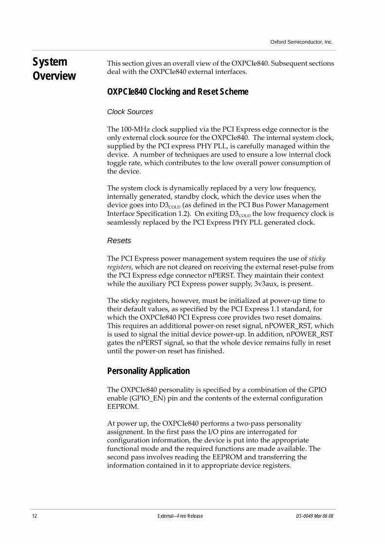
System Overview
This section gives an overall view of the OXPCIe840. Subsequent sections deal with the OXPCIe840 external interfaces.
OXPCIe840 Clocking and Reset Scheme
Clock Sources
The 100‐MHz clock supplied via the PCI Express edge connector is the only external clock source for the OXPCIe840. The internal system clock, supplied by the PCI express PHY PLL, is carefully managed within the device. A number of techniques are used to ensure a low internal clock toggle rate, which contributes to the low overall power consumption of the device.
The system clock is dynamically replaced by a very low frequency, internally generated, standby clock, which the device uses when the device goes into D3COLD (as defined in the PCI Bus Power Management Interface Specification 1.2). On exiting D3COLD the low frequency clock is seamlessly replaced by the PCI Express PHY PLL generated clock.
Resets
The PCI Express power management system requires the use of sticky registers, which are not cleared on receiving the external reset‐pulse from the PCI Express edge connector nPERST. They maintain their context while the auxiliary PCI Express power supply, 3v3aux, is present.
The sticky registers, however, must be initialized at power‐up time to their default values, as specified by the PCI Express 1.1 standard, for which the OXPCIe840 PCI Express core provides two reset domains. This requires an additional power‐on reset signal, nPOWER_RST, which is used to signal the initial device power‐up. In addition, nPOWER_RST gates the nPERST signal, so that the whole device remains fully in reset until the power‐on reset has finished.
Personality Application
The OXPCIe840 personality is specified by a combination of the GPIO enable (GPIO_EN) pin and the contents of the external configuration EEPROM.
At power up, the OXPCIe840 performs a two‐pass personality assignment. In the first pass the I/O pins are interrogated for configuration information, the device is put into the appropriate functional mode and the required functions are made available. The second pass involves reading the EEPROM and transferring the information contained in it to appropriate device registers.
DS-0049 Mar 06 08 External—Free Release 13
Oxford Semiconductor, Inc.
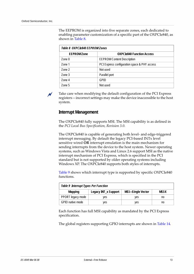
The EEPROM is organized into five separate zones, each dedicated to enabling parameter customization of a specific part of the OXPCIe840, as shown in Table 8.
Take care when modifying the default configuration of the PCI Express registers—incorrect settings may make the device inaccessible to the host system.
Interrupt Management
The OXPCIe840 fully supports MSI. The MSI capability is as defined in the PCI Local Bus Specification, Revision 3.0.
The OXPCIe840 is capable of generating both level‐ and edge‐triggered interrupt messaging. By default the legacy PCI‐based INTx level sensitive wired OR interrupt emulation is the main mechanism for sending interrupts from the device to the host system. Newer operating systems, such as Windows Vista and Linux 2.6 support MSI as the native interrupt mechanism of PCI Express, which is specified in the PCI standard but is not supported by older operating systems including Windows XP. The OXPCIe840 supports both styles of interrupts.
Table 9 shows which interrupt type is supported by specific OXPCIe840 functions.
Each function has full MSI capability as mandated by the PCI Express specification.
The global registers supporting GPIO interrupts are shown in Table 14.
Table 8 OXPCIe840 EEPROM Zones
EEPROM Zone OXPCIe840 Function AccessZone 0 EEPROM Content DescriptionZone 1 PCI Express configuration space & PHY accessZone 2 Not usedZone 3 Parallel portZone 4 GPIOZone 5 Not used
Table 9 Interrupt Types Per Function
Mapping Legacy INT_x Support MSI—Single Vector MSI-XPPORT legacy mode yes yes noGPIO native mode yes yes no
14 External—Free Release DS-0049 Mar 06 08
Oxford Semiconductor, Inc.
PCI Express Interface
The OXPCIe840 provides a fully‐featured X1 (single‐lane) PCI EXPRESS interface which is fully compliant with both the PCI EXPRESS Base Specification, Revision 1.1 and the PCI Bus Power Management Interface Specification, Revision 1.2.
Power Management
The OXPCIe840 includes the complete PCI Express Power management capabilities as defined in the PCI Bus Power Management Interface Specification, Revision. 1.2, including full support for D0 and D3 device states and PME message support.
Power Supply Management
All OXPCIe840 power supply requirements can be met from a single 3.3‐V power source, which is typically provided by the PCI Express edge connector.
The GPIO interface can be configured to operate at 1.8V, 2.5V or 3.3V by connecting the power supply pins associated with the appropriate functional pin grouping to the required interface voltage. In cases other than 3.3V, the system designer must ensure that a suitable voltage source is available.
The OXPCIe840 low‐power 1.2V internal core is supplied via the integral power supply system, PMU, which provides high efficiency energy conversion from 3.3V to 1.2V.
It is recommended that sequencing of the multi‐voltage IO power supplies should be performed. For power up, after the core voltage is stable (flagged by the POWER_GOOD pin) the IO supplies must be sequenced with the lowest supply (1.8V) first to the highest supply last (3.3V). Once all supplies are stable the power on reset (nPOWER_RST) pin can be de‐asserted to allow start of operation for the OXPCIe840. This sequencing (with timing) is given in Figure 3 on page 15.

DS-0049 Mar 06 08 External—Free Release 15
Oxford Semiconductor, Inc.
Figure 3 Power-up Sequence
For the OXPCIe840 there are only two multi‐voltage domains (VDDIO1 and VDDIO2). However, even if both VDDIO1 and VDDIO2 are to be at 3.3 V, they should still be enabled after the 1.2‐V core supply is stable and so should not be directly connected to the main 3.3‐V supply from the PCI Express connector.
OXPCIe840 Functions
Parallel Port Function
Parallel Port Overview
The OXPCIe840 offers a compact, low power, IEEE‐1284 compliant host‐interface parallel port designed to interface to many peripherals such as printers, scanners and external drives. It supports compatibility modes, SPP, NIBBLE, PS2, EPP and ECP modes. The parallel port is always used in PCI Express legacy mode. The register set is compatible with the Microsoft® register definition.
A sideband control signal is provided to control line drivers in applications where true 5.0‐V signalling is required. By default, the parallel port uses 3.3‐V output signalling, but its inputs tolerate 5.0‐V signalling.
VDDCORE (1.2 V)
POWER_GOOD
2ms (min)
50ms (max)
1ms (min)
1ms (min)
1ms (min)
1ms (min)
MV-VDDIO (1.8 V)
MV-VDDIO (2.5 V)
MV-VDDIO (3.3 V)
3.3 V (Main)
nPOWER_RST
16 External—Free Release DS-0049 Mar 06 08
Oxford Semiconductor, Inc.
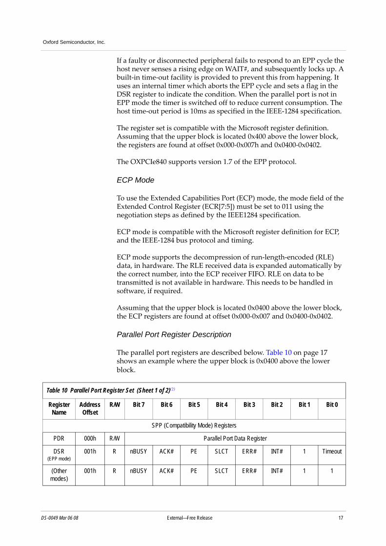
Operation and Mode selection
The system can access the parallel port via one 8‐byte and one 4‐byte block of I/O space; BAR0 contains the address of the basic parallel port registers, BAR1 contains the address of the upper registers. These are referred to as the lower block and upper block in this section. The 4‐byte upper block can be located at an address 0x400 above the 8‐byte lower block, allowing generic PC device drivers to be used to configure the port, because the addressable registers of legacy parallel ports always have this relationship.
SPP Mode
SPP (output‐only) is the standard implementation of a simple parallel port. In this mode, the PD lines always drive the value in the PDR register. All transfers are done under software control. Input must be performed in nibble mode.
Generic device driver‐software may use the address in I/O space encoded in BAR0 of function 0 to access the parallel port. The default configuration allocates 8 bytes to BAR0 in I/O space.
PS2 Mode
This mode is also referred to as bi‐directional or compatible parallel port. To use the PS2 mode, the mode field of the Extended Control Register (ECR[7:5]) must be set to 001 using the negotiation steps defined by the IEEE1284 specification. PS2 operation is similar to SPP mode but, in this mode, directional control of the parallel port data lines (PD[7:0]) is possible by setting & clearing DCR[5], the data direction bit.
EPP Mode
To use the enhanced parallel port (EPP) the mode bits (ECR[7:5]) must be set to 100 using the negotiation steps defined by the IEEE1284 specification.
The EPP address and data port registers are compatible with the IEEE 1284 definition. A write or read in relation to an EPP port register is passed through the parallel port to access the external peripheral. In EPP mode, the STB#, INIT#, AFD# and SLIN# pins change from open‐drain outputs to active push‐pull (totem pole) drivers (as required by IEEE 1284) and the pins ACK#, AFD#, BUSY, SLIN# and STB# are redefined as INTR#, DATASTB#, WAIT#, ADDRSTB# and WRITE# respectively.
An EPP port access begins with the host reading from or writing to one of the EPP port registers. The device automatically buffers the data between the I/O registers and the parallel port depending on whether it is a read or a write cycle. When the peripheral is ready to complete the transfer it takes the WAIT# status line high. This allows the host to complete the EPP cycle.
DS-0049 Mar 06 08 External—Free Release 17
Oxford Semiconductor, Inc.
If a faulty or disconnected peripheral fails to respond to an EPP cycle the host never senses a rising edge on WAIT#, and subsequently locks up. A built‐in time‐out facility is provided to prevent this from happening. It uses an internal timer which aborts the EPP cycle and sets a flag in the DSR register to indicate the condition. When the parallel port is not in EPP mode the timer is switched off to reduce current consumption. The host time‐out period is 10ms as specified in the IEEE‐1284 specification.
The register set is compatible with the Microsoft register definition. Assuming that the upper block is located 0x400 above the lower block, the registers are found at offset 0x000‐0x007h and 0x0400‐0x0402.
The OXPCIe840 supports version 1.7 of the EPP protocol.
ECP Mode
To use the Extended Capabilities Port (ECP) mode, the mode field of the Extended Control Register (ECR[7:5]) must be set to 011 using the negotiation steps as defined by the IEEE1284 specification.
ECP mode is compatible with the Microsoft register definition for ECP, and the IEEE‐1284 bus protocol and timing.
ECP mode supports the decompression of run‐length‐encoded (RLE) data, in hardware. The RLE received data is expanded automatically by the correct number, into the ECP receiver FIFO. RLE on data to be transmitted is not available in hardware. This needs to be handled in software, if required.
Assuming that the upper block is located 0x0400 above the lower block, the ECP registers are found at offset 0x000‐0x007 and 0x0400‐0x0402.
Parallel Port Register Description
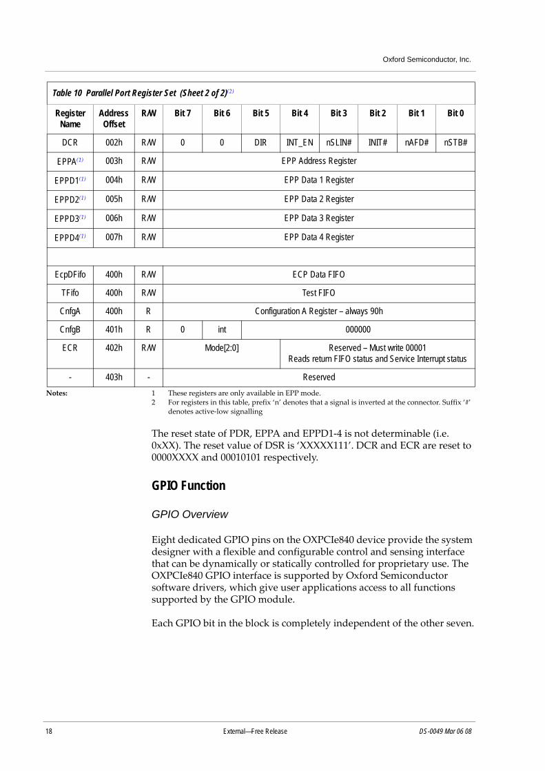
The parallel port registers are described below. Table 10 on page 17 shows an example where the upper block is 0x0400 above the lower block.
Table 10 Parallel Port Register Set (Sheet 1 of 2)(2)
Register Name
Address Offset
R/W Bit 7 Bit 6 Bit 5 Bit 4 Bit 3 Bit 2 Bit 1 Bit 0
SPP (Compatibility Mode) Registers
PDR 000h R/W Parallel Port Data Register
DSR (EPP mode)
001h R nBUSY ACK# PE SLCT ERR# INT# 1 Timeout
(Other modes)
001h R nBUSY ACK# PE SLCT ERR# INT# 1 1
18 External—Free Release DS-0049 Mar 06 08
Oxford Semiconductor, Inc.
Notes: 1 These registers are only available in EPP mode.2 For registers in this table, prefix ‘n’ denotes that a signal is inverted at the connector. Suffix ‘#’
denotes active‐low signalling
The reset state of PDR, EPPA and EPPD1‐4 is not determinable (i.e. 0xXX). The reset value of DSR is ‘XXXXX111’. DCR and ECR are reset to 0000XXXX and 00010101 respectively.
GPIO Function
GPIO Overview
Eight dedicated GPIO pins on the OXPCIe840 device provide the system designer with a flexible and configurable control and sensing interface that can be dynamically or statically controlled for proprietary use. The OXPCIe840 GPIO interface is supported by Oxford Semiconductor software drivers, which give user applications access to all functions supported by the GPIO module.
Each GPIO bit in the block is completely independent of the other seven.
DCR 002h R/W 0 0 DIR INT_EN nSLIN# INIT# nAFD# nSTB#
EPPA(1) 003h R/W EPP Address Register
EPPD1(1) 004h R/W EPP Data 1 Register
EPPD2(1) 005h R/W EPP Data 2 Register
EPPD3(1) 006h R/W EPP Data 3 Register
EPPD4(1) 007h R/W EPP Data 4 Register
EcpDFifo 400h R/W ECP Data FIFO
TFifo 400h R/W Test FIFO
CnfgA 400h R Configuration A Register – always 90h
CnfgB 401h R 0 int 000000
ECR 402h R/W Mode[2:0] Reserved – Must write 00001Reads return FIFO status and Service Interrupt status
- 403h - Reserved
Table 10 Parallel Port Register Set (Sheet 2 of 2)(2)
Register Name
Address Offset
R/W Bit 7 Bit 6 Bit 5 Bit 4 Bit 3 Bit 2 Bit 1 Bit 0

DS-0049 Mar 06 08 External—Free Release 19
Oxford Semiconductor, Inc.
GPIO Modes
Each GPIO pin can be independently programmed to operate in one of four modes as follows:
Input mode
Output mode
Open drain mode
Pulse‐width‐modulated (PWM) output mode
In input mode, the external GPIO pin level is always reported, and any CPU writes to the GPIO output register have no effect. When selected as an input pin, the GPIO block can additionally assign interrupt capabilities to it. GPIO pins set as inputs can be configured to act as system wake‐up lines.
Interrupts and/or wake‐ups can be generated following various trigger events:
Rising edge
Falling edge
Any edge
High level
Low level
In output mode, the external GPIO pin is driven hard to either high or low levels depending on the value present in the output register.
In open‐drain mode, the external pin is left in a floating (Hi‐Z) state if the output register is set to logic 0. When set to logic 1, the external pin is pulled down hard to logic 0.
In PWM output mode, the external GPIO pin is driven in a pulse‐width‐modulated pattern. Three dedicated registers are used to set the high and low durations of the PWM cycle and an 8‐bit pre‐scalar register. The values are scaled in steps based on the prescale value and each has a resolution of 12 bits for low and 12 bits for high.
The GPIO module uses a 62.5‐MHz baseline clock, which switches to a much lower frequency standby clock when the OXPCIe840 is put into standby mode, which means that the GPIO PWM output frequency should be considered indeterminate.
Clearing the level‐based interrupt mode while the level is still active causes a single clock cycle‐wide inactive pulse to be generated, which allows the GPIO function to generate a new edge‐based MSI when enabled.

20 External—Free Release DS-0049 Mar 06 08
Oxford Semiconductor, Inc.
GPIO BAR Detailed Breakdown
The GPIO BAR accesses various internal locations over its 1‐Kbyte aperture, as shown in Table 11.
Note:1 See “GPIO Registers” on page 21 for details.
Table 11 GPIO BAR Details(1)
BAR Offset Description0x000 Class code & rev ID0x004 Decimal number of GPIOs0x008 Global GPIO IRQ status0x00C Global GPIO IRQ enable0x010 Global GPIO IRQ disable0x014 Global GPIO wake enable0x018 Global GPIO wake disable
0x01C..0x0FF Reserved (returns zero)0x100..0x198 All GPIO registers(1)
0x1A0..0x1FF Reserved (returns zero)0x200...0x23F Reserved (returns zero)0x240..0x3FF Reserved (returns zero)
Table 12 Class Code & Revision ID (Bar Offset 0x000)
Bits Description Read/Write ResetEEPROM PCI Express
31:8 Classcode - R 0x0700027:0 Revision ID W R 0x0
Table 13 Decimal Number of GPIOs (Bar Offset 0x004)
Bits Description Read/Write ResetEEPROM PCI Express
31:5 Reserved - R 0x00000004:0 Number of GPIOs enabled (in decimal) W R 0x8
Table 14 Global GPIO IRQ Status (Bar Offset 0x008)
Bits Description Read/Write ResetEEPROM PCI Express
31:8 Reserved - R 0x00000007:0 GPIO[7:0] IRQ status - R 0x00

DS-0049 Mar 06 08 External—Free Release 21
Oxford Semiconductor, Inc.
GPIO Registers
The GPIO register set is described in this section. Table 19 on page 22 shows the complete GPIO register set. Each individual GPIO bit has its own dedicated configuration, PWM prescaler and PWM timing registers. Additionally, a number of registers for writing, reading and interrupt controlling are shared by all eight GPIO pins. This means that functions can be accessed through two registers: either the GPIO configuration registers (which allows access to multiple functions for a single GPIO); or the individual function registers (which allow access to a single function for multiple GPIO pins). For example, the input value of GPIO 0 can be read from bit 13 of GPIO[0] Configuration Register or bit 0 of GPIO[7:0] Input Value Register.
Table 15 Global GPIO IRQ Enable (Bar Offset 0x00C)
Bits Description Read/Write ResetEEPROM PCI Express
31:8 Reserved - R 0x00000007:0 GPIO[7:0] IRQ enable W RW 0x00
Table 16 Global GPIO IRQ Disable (Bar Offset 0x010)
Bits Description Read/Write ResetEEPROM PCI Express
31:8 Reserved - R 0x00000007:0 GPIO[7:0] IRQ disable W RW 0xFF
Table 17 Global GPIO Wake Enable (Bar Offset 0x014)
Bits Description Read/Write ResetEEPROM PCI Express
31:1 Reserved - R 0x00000000 Global GPIO wake enable bit W RW 1
Table 18 Global GPIO Wake Disable (Bar Offset 0x018)
Bits Description Read/Write ResetEEPROM PCI Express
31:1 Reserved - R 0x00000000 Global GPIO wake disable bit W RW 0

22 External—Free Release DS-0049 Mar 06 08
Oxford Semiconductor, Inc.
GPIO Configuration Registers
Table 20 on page 23 shows the bit assignment used by the eight GPIO Configuration registers, which reside at locations 0x00, 0x10, 0x20, 0x30, 0x40, 0x50, 0x60 and 0x70 respectively.
Table 19 GPIO Registers (Bar Offset 0x100)
Address offset
Bits Type Description
0x100 16 RW GPIO[0] Configuration0x104 8 RW GPIO[0] PWM Prescaler0x108 32 RW GPIO[0] PWM Timing0x110 16 RW GPIO[1] Configuration0x114 8 RW GPIO[1] PWM Prescaler0x118 32 RW GPIO[1] PWM Timing0x120 16 RW GPIO[2] Configuration0x124 8 RW GPIO[2] PWM Prescaler0x128 32 RW GPIO[2] PWM Timing0x130 16 RW GPIO[3] Configuration0x134 8 RW GPIO[3] PWM Prescaler0x138 32 RW GPIO[3] PWM Timing0x140 16 RW GPIO[4] Configuration0x144 8 RW GPIO[4] PWM Prescaler0x148 32 RW GPIO[4] PWM Timing0x150 16 RW GPIO[5] Configuration0x154 8 RW GPIO[5] PWM Prescaler0x158 32 RW GPIO[5] PWM Timing0x160 16 RW GPIO[6] Configuration0x164 8 RW GPIO[6] PWM Prescaler0x168 32 RW GPIO[6] PWM Timing0x170 16 RW GPIO[7] Configuration0x174 8 RW GPIO[7] PWM Prescaler0x178 32 RW GPIO[7] PWM Timing0x180 8 RW GPIO[7:0] Output Value0x184 8 R GPIO[7:0] Input Value0x190 8 RW1C GPIO[7:0] Interrupt Status0x194 8 RW1S GPIO[7:0] Interrupt Enable0x198 8 RW1S GPIO[7:0] Interrupt Disable

DS-0049 Mar 06 08 External—Free Release 23
Oxford Semiconductor, Inc.
Notes:1 Writing 00 or 11 to bit[9..8] (GPIO interrupt disable and GPIO interrupt enable) does not
change current settings.2 Bit 10 (interrupt status) is RW1C (read/write 1 to clear) type, which means that the IRQ status
bit can only be cleared by writing 1 to it. If the interrupt is level‐based and the IRQ event criterion is still met, a new interrupt is generated immediately after clearing this bit.
3 Bit 11, wake‐up status, is also RW1C type.
Table 20 GPIO Configuration Registers
Bits Description Read/Write ResetEEPROM PCI Express
31:14 Reserved R 0x0000013 GPIO input value
1 = input at logic ‘1’0 = input at logic ‘0’
R 0
12 GPIO output value1 = output driving logic ‘1’0 = output driving logic ‘0’
RW 0
11 GPIO wake-up status1 = active0 = inactive
RW1C 0
10 GPIO interrupt status1 = active0 = inactive
RW1C 0
9 GPIO interrupt disableWR 1 = disable
0 = do not change current settingsRD 1 = GPIO interrupt is disabled
0 = GPIO interrupt is enabled
W RW 0
8 GPIO interrupt enableWR 1 = enable
0 = do not change current settingsRD 1 = GPIO interrupt is enabled
0 = GPIO interrupt is disabled
W RW 0
7 GPIO wake-up enable1 = enabled0 = disabled
W RW 0
6:4 GPIO interrupt and wake-up mode000 = Rising edge001 = Falling edge010 =High level (continuous asser-tion)011 =Low level (continuous asser-tion)1xx =Any edge
W RW 000
3:2 Reserved R 00
1:0 GPIO pin mode00 =Input mode01 =Output mode10 =Open drain mode11 = PWM output mode
W RW 00
24 External—Free Release DS-0049 Mar 06 08
Oxford Semiconductor, Inc.
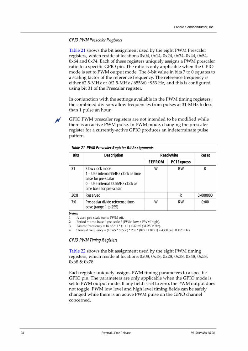
GPIO PWM Prescaler Registers
Table 21 shows the bit assignment used by the eight PWM Prescaler registers, which reside at locations 0x04, 0x14, 0x24, 0x34, 0x44, 0x54, 0x64 and 0x74. Each of these registers uniquely assigns a PWM prescaler ratio to a specific GPIO pin. The ratio is only applicable when the GPIO mode is set to PWM output mode. The 8‐bit value in bits 7 to 0 equates to a scaling factor of the reference frequency. The reference frequency is either 62.5‐MHz or (62.5‐MHz / 65536) ~953 Hz, and this is configured using bit 31 of the Prescalar register.
In conjunction with the settings available in the PWM timing registers, the combined divisors allow frequencies from pulses at 31‐MHz to less than 1 pulse an hour.
GPIO PWM prescaler registers are not intended to be modified while there is an active PWM pulse. In PWM mode, changing the prescaler register for a currently‐active GPIO produces an indeterminate pulse pattern.
Notes:1 A zero pre‐scale turns PWM off.2 Period = time‐base * pre‐scale * (PWM low + PWM high).3 Fastest frequency = 16 nS * 1 * (1 + 1) = 32 nS (31.25 MHz).4 Slowest frequency = (16 nS * 65536) * 255 * (8191 + 8191) = 4380 S (0.00028 Hz).
GPIO PWM Timing Registers
Table 22 shows the bit assignment used by the eight PWM timing registers, which reside at locations 0x08, 0x18, 0x28, 0x38, 0x48, 0x58, 0x68 & 0x78.
Each register uniquely assigns PWM timing parameters to a specific GPIO pin. The parameters are only applicable when the GPIO mode is set to PWM output mode. If any field is set to zero, the PWM output does not toggle. PWM low level and high level timing fields can be safely changed while there is an active PWM pulse on the GPIO channel concerned.
Table 21 PWM Prescaler Register Bit Assignments
Bits Description Read/Write ResetEEPROM PCI Express
31 Slow clock mode1 = Use internal 954Hz clock as time base for pre-scalar0 = Use internal 62.5MHz clock as time base for pre-scalar
W RW 0
30:8 Reserved R 0x0000007:0 Pre-scalar divide reference time-
base (range 1 to 255)W RW 0x00

DS-0049 Mar 06 08 External—Free Release 25
Oxford Semiconductor, Inc.
Note:1 A zero in either the low‐ or high‐level timing field turns PWM off.
GPIO[7:0] Output Value Register
Table 23 shows the bit assignment for the GPIO[7:0] Output Value register, which resides at location 0x80.
Notes:1 GPIO configuration register bits [1:0] = ‘10’.2 GPIO configuration register bits [1:0] = ‘01’.
GPIO[7:0] Input Value Register
Table 24 shows the bit assignment for the GPIO[7:0] Input Value register, which resides at location 0x84.
Table 22 PWM Timing Registers
Bits Description Read/Write ResetEEPROM PCI Express
31:29 Reserved R 00028:16 PWM low-level timing in steps of pre-
scalar interval (range 1 to 8191)(1)W RW 0x0000
15:13 Reserved R 00012:0 PWM high-level timing in steps of pre-
scalar interval (range 1 to 8191)(1)W RW 0x0000
Table 23 GPIO[7:0] Output Value Register Bit Assignment
Bits Description Read/Write ResetEEPROM PCI Express
31:8 Reserved R 0x0000007:0 GPIO[7:0]: Open drain or Output
mode value status.The following values represent a single register bit per pin:Open drain mode(1)
1 = output driven to logic ‘1’0 = floating output
Output mode(2)1 = output driven to logic ‘1’0 = output driven to logic ‘0’
RW 0x00
Table 24 GPIO[7:0] Input Value Register Bit Assignment
Bits Description Read/Write ResetEEPROM PCI Express
31:8 Reserved R 0x0000007:0 GPIO[7:0]: Input value.
The following values represent a single register bit per pin:1 = Input value is logic ‘1’0 = Input value is logic ‘0’
R 0x00

26 External—Free Release DS-0049 Mar 06 08
Oxford Semiconductor, Inc.
GPIO[7:0] Interrupt Status Register
Table 25 shows the bit assignment for the GPIO[7:0] Interrupt Status register, which resides at location 0x90.
This register is RW1C type, which means that IRQ status bits can only be cleared by writing 1 to the appropriate bit. If the interrupt is level‐based and the IRQ event criteria is still met, a new interrupt is generated immediately after clearing this register.
GPIO[7:0] Interrupt Enable Register
Table 26 shows the bit assignment for the GPIO[7:0] Interrupt Enable register, which resides at location 0x94.
This register is RW1S type, which means that IRQ enable bits can only be set by writing 1 to the appropriate bit. Reading the register returns 1 for the bits that are enabled, and 0 for those that are disabled.
GPIO[7:0] Interrupt Disable Register
Table 27 on page 27 shows the bit assignment for the GPIO Interrupt Disable register, which resides at location 0x98.
This register is RW1S type, which means that IRQ disable bits can only be set by writing 1 to the appropriate bit. Reading the register returns 1 for the bits that are disabled, and 0 for those that are enabled.
Table 25 GPIO[7:0] Interrupt Status Value Registers Bit Assignment
Bits Description Read/Write ResetEEPROM PCI Express
31:8 Reserved R 0x0000007:0 GPIO[7:0]: Interrupt status.
The following values represent a single register bit per pin:1 = active0 = inactive
RW1C 0x00
Table 26 GPIO[7:0] Interrupt Enable Register Bit Assignment
Bits Description Read/Write ResetEEPROM PCI Express
31:8 Reserved R 0x0000007:0 GPIO[7:0]: interrupt enable.
The following values represent a single register bit per pin:1 = enable0 = do not change
W RW1S 0x00

DS-0049 Mar 06 08 External—Free Release 27
Oxford Semiconductor, Inc.
EEPROM Interface & Programming Capabilities
Overview
The OXPCIe840 EEPROM read and programming capability allows developers to customize the default personality the device exhibits after system reset by bootstrapping any of the device registers available in the chosen mode option. The OXPCIe840 dedicated EEPROM controller performs this task in two passes. The first pass uses data in an internal ROM store containing mandatory personalization of the PCI Express core for a specific mode setting. The second pass involves accessing the off‐chip EEPROM for the customer personality application.
The OXPCIe840 is fully supported by the Oxford Semiconductor Oxide utility. This deploys the zone concept currently used with other Oxford Semiconductor products, by which each external EEPROM zone accesses a specific peripheral interface using a peek and poke mechanism. In addition, a more automatic device read/write capability is provided on the OXPCIe840.
The automatic EEPROM read/writing capability allows software developers to apply upgrades to the final product more easily, or handle peek and poke debugging in a development environment. The system software can set up an operation and then inform the EEPROM interface to execute it. The OXPCIe840 internal EEPROM control function then performs the task in the background, with system software polling the EEPROM controller until the command is complete—for a read operation, software may then read the data register; for a write operation, software may then start another operation. EEPROM devices need to be opened and closed for writing. To aid this, the auto‐write enable/disable operation is done by setting a command bit and then polling the status flag as if it had been an EEPROM read or write operation.
For further customer solution protection, the EEPROM write feature can optionally be masked to prevent accidental or malicious alteration. The boot‐EEPROM can write to a write‐protect register to stop host software from modifying the contents of the external EEPROM.
Table 27 GPIO Interrupt Disable Register Bit Assignment
Bits Description Read/Write ResetEEPROM PCI Express
31:8 Reserved R 0x0000007:0 GPIO[7:0]: interrupt disable.
The following values represent a single register bit per pin:1 = disable0 = do not change
W RW1S 0x00

28 External—Free Release DS-0049 Mar 06 08
Oxford Semiconductor, Inc.
Boot ROM: Phase 1
At power‐on, device mode settings determine the basic personality of the OXPCIe840. The new personality must be imprinted before the external EEPROM makes any other modifications, because the first phase enables specific functions and BARs within the PCI Express core on the OXPCIe840.
The boot ROM is programmed with information to configure PCI Express registers for all functions present in the device. Functions depend on the state of the GPIO_EN pin. No functions require BAR 3, BAR 4 or BAR 5, so they are permanently disabled.
The registers modified by personality assignment are listed below:
VENDOR‐ID, DEVICE‐ID
CLASS‐CODE & REVISION ID
SUBSYSTEM‐VENDOR‐ID, SUBSYSTEM‐DEVICE‐ID
All applicable BAR regions (mask and type)
Figure 2 on page 9 shows the OXPCIe840 configuration space, which is allocated for each function. All targets are 32 bits wide, so the ROM is always formatted with 32‐bit data.
Boot ROM: Phase 2
The second phase of bootstrapping uses the Microwire interface to upload customer configurations from an off‐chip EEPROM device. The EEPROM interface operates with a divisor of 70 (decimal) to produce a clock rate of ~890 kHz. The slowest supported Microwire device is 1 MHz—at this rate an EEPROM access takes approximately 31 μS.
For safety, the first operation of the phase 2 configuration is to perform a dummy read to the EEPROM to detect whether a device is present. This also detects the number of address bits on the device. Booting occurs using this information if a device is detected.
The first location of the EEPROM must have a Zone 0 header; and the ID field extracted by the phase 2 configuration must match. If it does not, the EEPROM image is considered corrupt and the phase 2 boot aborts, setting the bootstrap error status bit. If the EEPROM image passes this first check but is still corrupt, the booting sequence continues blindly, accessing the off chip EEPROM until the address register loops back round to zero. At this point it recognizes that the image is corrupt and abandons configuration, setting the bootstrap error status bit.

DS-0049 Mar 06 08 External—Free Release 29
Oxford Semiconductor, Inc.
CRC16
The EEPROM image ends with a CRC16 value. The value is calculated on every word in the EEPROM that is read out by the EEPROM interface. The CRC16 value is initialized to all Fs and uses the PCI Express DLLP CRC16 polynomial:
100B = x16 + x12 + x3 + x + 1
If the CRC16 word fails to match the expected CRC16, the bootstrap is considered to have failed and the bootstrap error bit is set. However the device will attempt to continue to function using the settings read from the EEPROM.
CRC generation starts with bit 0 of first header word and progresses to bit 15 of the header word. CRC generation then moves to bit 0 of word 1 and so on.
EEPROM Zone Allocation
The basic format of the EEPROM image for bootstrapping and using the Oxford Semiconductor EEPROM programming utilities is shown in Table 8.
The first location in the EEPROM is the Zone 0 header, as shown in Table 28. The EEPROM controller validates the EEPROM contents by checking the ID field of the Zone 0 header word.
Each zone uses the same method for capturing the configuration data. If the EEPROM attempts to program illegal states, undefined operations within the device may occur. Read‐only registers cannot be overwritten.
Table 28 EEPROM Zone 0 Format
Bits Description15:5 These bits denote the ID-field and must be encoded with the following bit
sequence: 1001 0111 1104 1—Zone 1 present
0—Zone 1 does not exist3 0—Zone 2 unused2 1—Zone 3 present
0—Zone 3 does not exist1 1—Zone 4 present
0—Zone 4 does not exist0 0—Zone 5 unused
30 External—Free Release DS-0049 Mar 06 08
Oxford Semiconductor, Inc.
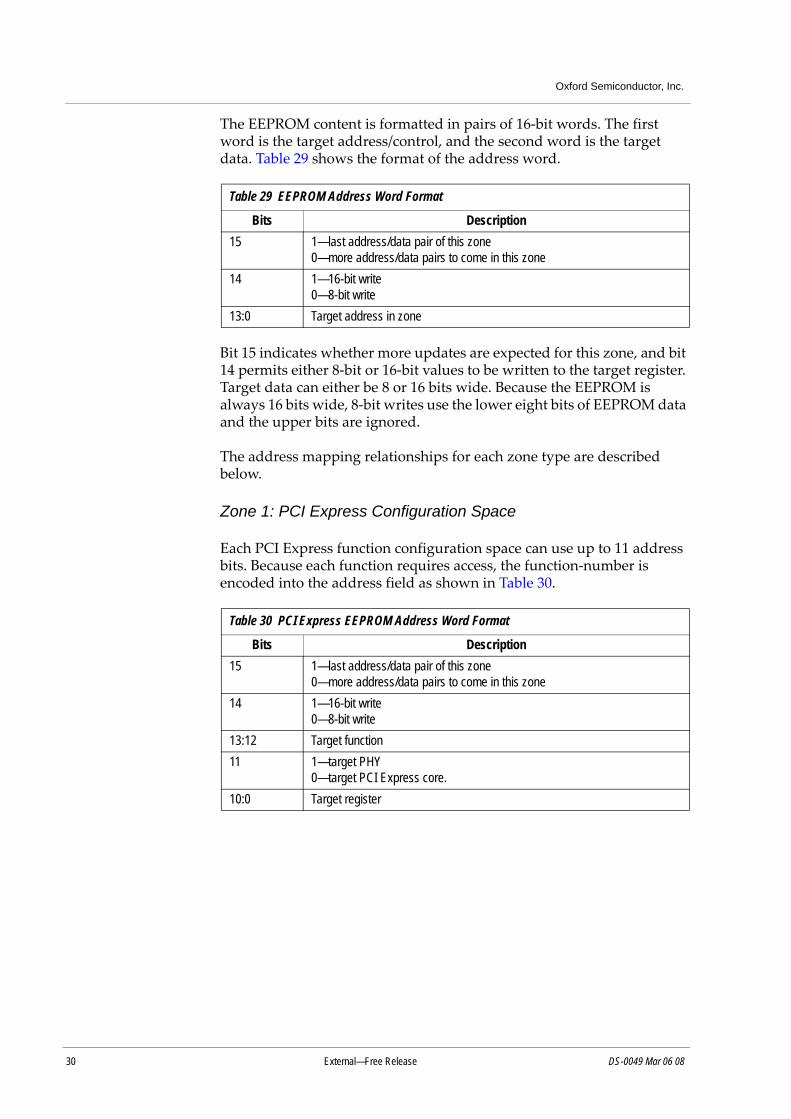
The EEPROM content is formatted in pairs of 16‐bit words. The first word is the target address/control, and the second word is the target data. Table 29 shows the format of the address word.
Bit 15 indicates whether more updates are expected for this zone, and bit 14 permits either 8‐bit or 16‐bit values to be written to the target register. Target data can either be 8 or 16 bits wide. Because the EEPROM is always 16 bits wide, 8‐bit writes use the lower eight bits of EEPROM data and the upper bits are ignored.
The address mapping relationships for each zone type are described below.
Zone 1: PCI Express Configuration Space
Each PCI Express function configuration space can use up to 11 address bits. Because each function requires access, the function‐number is encoded into the address field as shown in Table 30.
Table 29 EEPROM Address Word Format
Bits Description15 1—last address/data pair of this zone
0—more address/data pairs to come in this zone14 1—16-bit write
0—8-bit write13:0 Target address in zone
Table 30 PCI Express EEPROM Address Word Format
Bits Description15 1—last address/data pair of this zone
0—more address/data pairs to come in this zone14 1—16-bit write
0—8-bit write13:12 Target function 11 1—target PHY
0—target PCI Express core.10:0 Target register

DS-0049 Mar 06 08 External—Free Release 31
Oxford Semiconductor, Inc.
Table 31 shows which PCI Configuration registers are writable from the EEPROM for each function.
Zone 2: Not Used
Zone 3: Parallel Port
Register mapping is one‐to‐one to the parallel port, in that the SPP and EPP registers reside at 0x000 and the ECP registers start at 0x008. See “Parallel Port Function” on page 15 for further details.
The allocation of the address field is shown in Table 32.
Table 31 PCI Configuration Registers Writable from the EEPROM for each Function
Offset Bits Description0x02 7:0 Device ID bits 7 to 00x03 7:0 Device ID bits 15 to 80x06 3:0 Must be ‘0000’0x06 4 Extended Capabilities0x06 7:5 Must be ‘000’0x09 7:0 Class Code bits 7 to 00x0A 7:0 Class Code bits 15 to 80x0B 7:0 Class Code bits 23 to 160x2E 7:0 Subsystem ID bits 7 to 00x2F 7:0 Subsystem ID bits 15 to 80x3D 7:0 Interrupt pin0x42 7:0 Power Management Capabilities bits 7 to 00x43 7:0 Power Management Capabilities bits 15 to 8
Table 32 Parallel Port EEPROM Address Word Format
Bits Description15 1—Last pair of this zone
0—More pairs to come in this zone14 1—16-bit write
0—8-bit write13:4 Reserved—must be set to zero3:0 Parallel port register
32 External—Free Release DS-0049 Mar 06 08
Oxford Semiconductor, Inc.
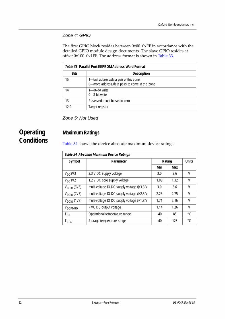
Zone 4: GPIO
The first GPIO block resides between 0x00..0xFF in accordance with the detailed GPIO module design documents. The slave GPIO resides at offset 0x100..0x1FF. The address format is shown in Table 33.
Zone 5: Not Used
Operating Conditions
Maximum Ratings
Table 34 shows the device absolute maximum device ratings.
Table 33 Parallel Port EEPROM Address Word Format
Bits Description15 1—last address/data pair of this zone
0—more address/data pairs to come in this zone14 1—16-bit write
0—8-bit write13 Reserved; must be set to zero12:0 Target register
Table 34 Absolute Maximum Device Ratings
Symbol Parameter Rating UnitsMin Max
VDD3V3 3.3 V DC supply voltage 3.0 3.6 V
VDD1V2 1.2 V DC core supply voltage 1.08 1.32 V
VDDIO (3V3) multi-voltage IO DC supply voltage @3.3 V 3.0 3.6 V
VDDIO (2V5) multi-voltage IO DC supply voltage @2.5 V 2.25 2.75 V
VDDIO (1V8) multi-voltage IO DC supply voltage @1.8 V 1.71 2.16 V
VDDPMUO PMU DC output voltage 1.14 1.26 V
TOP Operational temperature range -40 85 °C
TSTG Storage temperature range -40 125 °C

DS-0049 Mar 06 08 External—Free Release 33
Oxford Semiconductor, Inc.
Electrical Characteristics
Table 35 shows the multi‐voltage device I/O buffer electrical characteristics.
Table 36 shows the 5‐V tolerant device I/O buffer electrical characteristics.
Table 35 Multivoltage (3.3V, 2.5V, 1.8V) Device I/O Buffer Electrical Characteristics
Symbol Parameter Condition Rating Units
Min Typ Max
VMSSIO I/O Ground -0.3 0.3 V
VMIH Input high voltage 0.8*VDDIO VDDIO V
VMIL Input low voltage VSSIO 0.2*VDDIO V
IMI Input leakage current ±1 µA
VMIMAX (1.8) Input voltage tolerance @1.8 V 2.5 V
VMIMAX (2.5) Input voltage tolerance @ 2.5 V 3.3 V
VMOH Output high voltage VDDIO – (0.15*VDDIO) VDDIO V
VMOL Output low voltage VSSIO VSSIO + (0.15*VDDIO) V
Table 36 3.3V (5V tolerant) Only Device I/O Buffer Electrical Characteristics
Symbol Parameter Condition Rating Units
Min Typ Max
VIH Input high voltage 2.0 5.5 V
VIL Input low voltage -0.3 0.8 V
VT Threshold point 1.17 1.23 V
VT+ Schmitt trig. low to high threshold point 1.51 1.59 V
VT- Schmitt trig. High to low threshold point 0.92 0.98 V
II Input leakage current ±10 µA
IOZ Tristate output leakage current VO = 3.3 V or 0 V ±10 µA
VIMAX Maximum input voltage 5.5V V
VOH Output high voltage 2.4 V
VOL Output low voltage 0.4 V
34 External—Free Release DS-0049 Mar 06 08
Oxford Semiconductor, Inc.
AC Electrical Characteristics
Parallel Port
Table 37 shows the EPP Mode dynamic characteristics.VDDIO0 = 3 V to 3.6 V, VDDCORE = 1.08 V to 1.32 V; Tamb = ‐40 °C to +85 °C unless otherwise specified.Typical values are VDDIO0 = 3.3 V; VDDCORE = 1.2 V; Tamb = 25 °C unless otherwise specified.
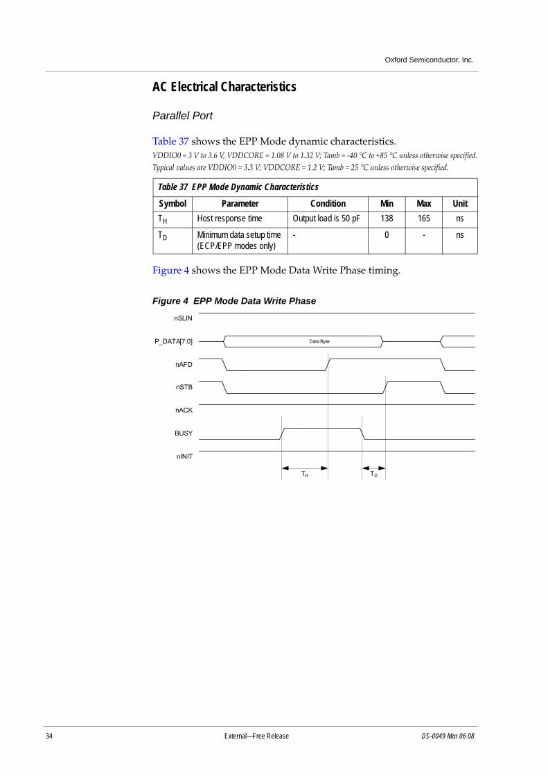
Figure 4 shows the EPP Mode Data Write Phase timing.
Figure 4 EPP Mode Data Write Phase
Table 37 EPP Mode Dynamic Characteristics
Symbol Parameter Condition Min Max UnitTH Host response time Output load is 50 pF 138 165 ns
TD Minimum data setup time (ECP/EPP modes only)
- 0 - ns
Data Byte
TH TD
nSLIN
P_DATA[7:0]
nAFD
nSTB
nACK
BUSY
nINIT

DS-0049 Mar 06 08 External—Free Release 35
Oxford Semiconductor, Inc.
Figure 5 shows the EPP Mode Data Read Phase timing.
Figure 5 EPP Mode Data Read Phase
Figure 6 shows the EPP Mode Address Write Phase timing.
Figure 6 EPP Mode Address Write Phase
Data Byte
TH TDTD
nSLIN
P_DATA[7:0]
nAFD
nSTB
nACK
BUSY
nINIT
nSLIN
Address ByteP_DATA[7:0]
nAFD
nSTB
nACK
BUSY
nINIT TD TH

36 External—Free Release DS-0049 Mar 06 08
Oxford Semiconductor, Inc.
EEPROM (Microwire) Interface
Table 38 shows the EEPROM (Microwire) interface dynamic characteristics. All timing shown is with respect to the rising edge of EECK.VDDIO2 = 3V to 3.6V, VDDCORE = 1.08V to 1.32V; Tamb = -40°C to +85°C; unless otherwise specified.Typical values are VDDIO2 = 3.3V; VDDCORE = 1.2V; Tamb = 25°C; unless otherwise specified.
Figure 5 shows the EEPROM (Microwire) interface timing.
Figure 7 EEPROM (Microwire) Interface Timing
Table 38 EEPROM (Microwire) Interface Dynamic Characteristics
Symbol Parameter Condition Min Max Unit
tCCS Rising EECS to EECK Output load is 15pF 656 - ns
tCSH EECK to falling EECS Output load is 15pF 1344 ns
tCDS EECS deselect Output load is 15pF 1344 - ns
tDIS EEDI setup - 48 ns
tDIH EEDI hold - 0 - ns
tDDO EEDO output delay Output load is 15pF 656 688 ns
tCK Clock Period - 1344 - ns
valid
valid
tDIS tDIHtDDO tCSHtCSS
EECK
EECS
EEDO
EEDI
tCDS
DS-0049 Mar 06 08 External—Free Release 37
Oxford Semiconductor, Inc.
Package Mechanical Drawings
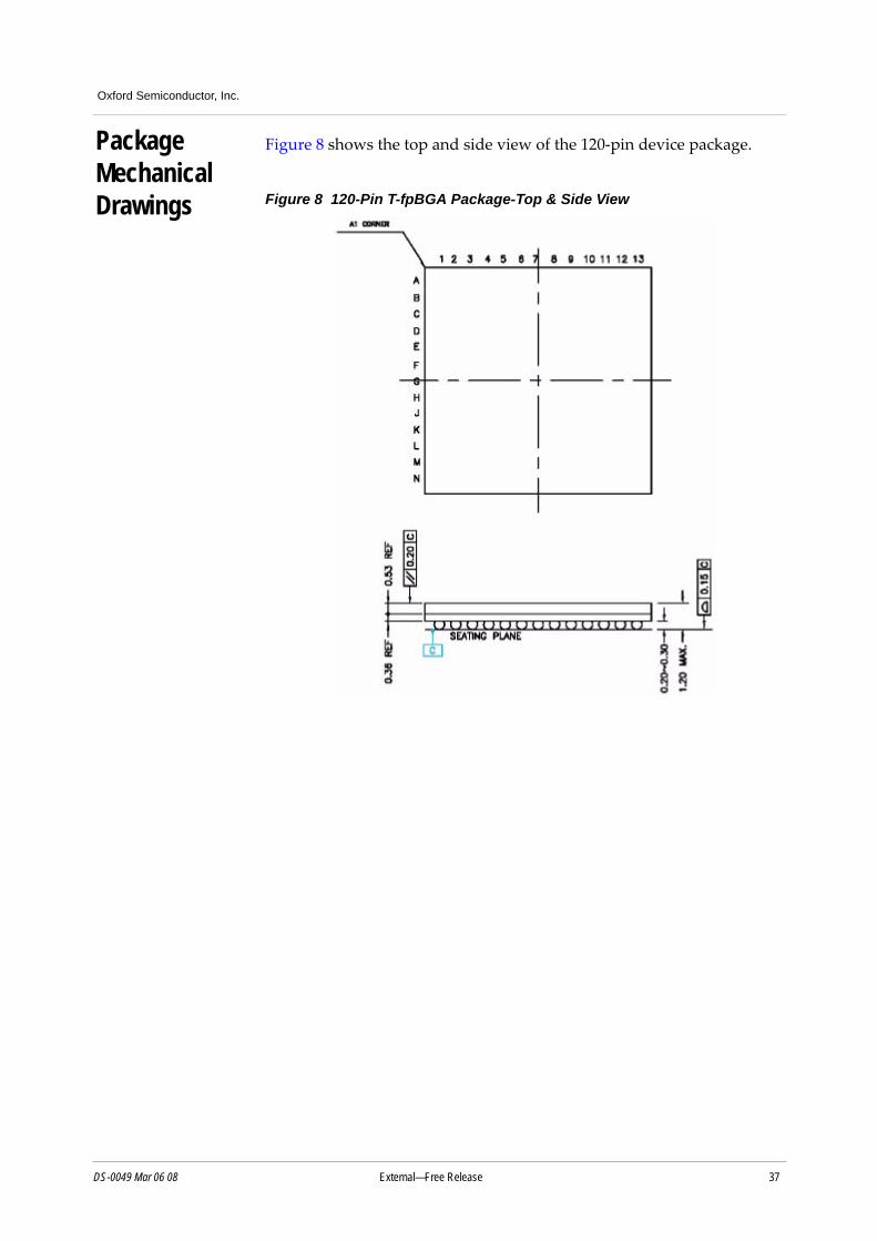
Figure 8 shows the top and side view of the 120‐pin device package.
Figure 8 120-Pin T-fpBGA Package-Top & Side View

38 External—Free Release DS-0049 Mar 06 08
Oxford Semiconductor, Inc.
Figure 9 shows the bottom view of the 120‐pin device package.
Figure 9 120-Pin T-fpBGA Package-Bottom
Ordering Information
The order code for the Oxford Semiconductor OXPCIe840 is OXPCIe840‐FBAG.
The following conventions are used to identify Oxford Semiconductor products:
Contacting Oxford Semiconductor
Oxford Semiconductor contact details:
Oxford Semiconductor, Inc.1900 McCarthy Boulevard, Suite 210Milpitas, CA 95035USA
Website: http://www.oxsemi.com Email: [email protected]
Alternatively, you can contact your local representative.
OXPCIe840 - F B A G
Revision: A
Package Type: FB 120 FBGA
Part Number
Green (RoHS compliant)

DS-0049 Mar 06 08 External—Free Release 39
Oxford Semiconductor, Inc.
Revision Information
Table 39 documents the revisions of this guide.
Table 39 Revision Information
Revision ModificationMarch 2008 First publication

Oxford Semiconductor, Inc.
© Oxford Semiconductor, Inc. 2008
The content of this manual is furnished for informational use only, is subject to change without notice, and should not be construed as a commitment by Oxford Semiconductor, Inc. Oxford Semiconductor, Inc. assumes no responsibility or liability for any errors or inaccuracies that may appear in this book.
40 External—Free Release DS-0049 Mar 06 08