Agenda Digital Design CountersandRegisters · §Using Registers to implement Sequential Circuits...
13
EE260: Digital Design, Spring 2018 4/8/18 Chapter 11: Counters and Registers 1 EE 260: Introduction to Digital Design Counters and Registers Yao Zheng Department of Electrical Engineering University of Hawaiʻi at Mānoa Counters § Introduction: Counters § Asynchronous (Ripple) Counters § Asynchronous Counters with MOD number < 2 n § Asynchronous Down Counters § Cascading Asynchronous Counters § Synchronous (Parallel) Counters § Up/Down Synchronous Counters § Designing Synchronous Counters § Decoding A Counter § Counters with Parallel Load Agenda Registers § Introduction: Registers v Simple Registers v Registers with Parallel Load § Using Registers to implement Sequential Circuits § Shift Registers v Serial In/Serial Out Shift Registers v Serial In/Parallel Out Shift Registers v Parallel In/Serial Out Shift Registers v Parallel In/Parallel Out Shift Registers § Bidirectional Shift Registers § An Application – Serial Addition § Shift Register Counters v Ring Counters v Johnson Counters § Random - Access Memory (RAM) Agenda Introduction: Counters § Counters are circuits that cycle through a specified number of states. § Two types of counters: v synchronous (parallel) counters v asynchronous (ripple) counters § Ripple counters allow some flip - flop outputs to be used as a source of clock for other flip - flops. § Synchronous counters apply the same clock to all flip - flops. Asynchronous (Ripple) Counters § Asynchronous counters : the flip - flops do not change states at exactly the same time as they do not have a common clock pulse. § Also known as ripple counters , as the input clock pulse “ripples” through the counter – cumulative delay is a drawback. § n flip - flops ® a MOD (modulus) 2 n counter. (Note: A MOD - x counter cycles through x states.) § Output of the last flip - flop (MSB) divides the input clock frequency by the MOD number of the counter, hence a counter is also a frequency divider . Asynchronous (Ripple) Counters § Example: 2 - bit ripple binary counter. § Output of one flip - flop is connected to the clock input of the next more - significant flip - flop. K J K J HIGH Q0 Q1 Q0 FF1 FF0 CLK C C Timing diagram 00 ® 01 ® 10 ® 11 ® 00 ... 4 3 2 1 CLK Q0 Q0 Q1 1 1 1 1 0 0 0 0 0 0
Transcript of Agenda Digital Design CountersandRegisters · §Using Registers to implement Sequential Circuits...

EE260: Digital Design, Spring 2018 4/8/18
Chapter 11: Counters and Registers 1
EE 260: Introduction toDigital Design
Counters and Registers
Yao ZhengDepartment of Electrical Engineering
University of Hawaiʻi at Mānoa
Counters
§ Introduction: Counters
§ Asynchronous (Ripple) Counters
§ Asynchronous Counters with MOD number < 2n
§ Asynchronous Down Counters
§ Cascading Asynchronous Counters
§ Synchronous (Parallel) Counters
§ Up/Down Synchronous Counters
§ Designing Synchronous Counters
§ Decoding A Counter
§ Counters with Parallel Load
Agenda
Registers
§ Introduction: Registersv Simple Registersv Registers with Parallel Load
§ Using Registers to implement Sequential Circuits
§ Shift Registersv Serial In/Serial Out Shift Registersv Serial In/Parallel Out Shift Registersv Parallel In/Serial Out Shift Registersv Parallel In/Parallel Out Shift Registers
§ Bidirectional Shift Registers
§ An Application – Serial Addition
§ Shift Register Countersv Ring Countersv Johnson Counters
§ Random-Access Memory (RAM)
Agenda Introduction: Counters§ Counters are circuits that cycle through a
specified number of states.§ Two types of counters:
vsynchronous (parallel) countersvasynchronous (ripple) counters
§ Ripple counters allow some flip-flop outputs to be used as a source of clock for other flip-flops.
§ Synchronous counters apply the same clock to all flip-flops.
Asynchronous (Ripple) Counters§ Asynchronous counters: the flip-flops do not change
states at exactly the same time as they do not have a common clock pulse.
§ Also known as ripple counters, as the input clock pulse “ripples” through the counter – cumulative delay is a drawback.
§ n flip-flops ® a MOD (modulus) 2n counter. (Note: A MOD-x counter cycles through x states.)
§ Output of the last flip-flop (MSB) divides the input clock frequency by the MOD number of the counter, hence a counter is also a frequency divider.
Asynchronous (Ripple) Counters§ Example: 2-bit ripple binary counter.§ Output of one flip-flop is connected to the clock
input of the next more-significant flip-flop.
K
J
K
J
HIGH
Q0 Q1
Q0
FF1FF0
CLK CC
Timing diagram00 ® 01 ® 10 ® 11 ® 00 ...
4321CLK
Q0
Q0
Q1
1 1
1 1
0
0 0
0 0
0

EE260: Digital Design, Spring 2018 4/8/18
Chapter 11: Counters and Registers 2
Asynchronous (Ripple) Counters§ Example: 3-bit ripple binary counter.
K
J
K
JQ0 Q1
Q0
FF1FF0
CCK
J
Q1 C
FF2
Q2CLK
HIGH
4321CLK
Q0
Q1
1 1
1 1
0
0 0
0 0
0
8765
1 10 0
1 10 0
Q2 0 00 0 1 1 11 0
Recycles back to 0
Asynchronous (Ripple) Counters§ Propagation delays in an asynchronous
(ripple-clocked) binary counter.§ If the accumulated delay is greater than the
clock pulse, some counter states may be misrepresented!
4321CLK
Q0
Q1
Q2
tPLH(CLK to Q0)
tPHL (CLK to Q0)tPLH (Q0 to Q1)
tPHL (CLK to Q0)tPHL (Q0 to Q1)tPLH (Q1 to Q2)
Asynchronous (Ripple) Counters§ Example: 4-bit ripple binary counter (negative-edge
triggered).
K
J
K
J Q1Q0
FF1FF0
CCK
JC
FF2
Q2
CLK
HIGH
K
J
C
FF3
Q3
CLK1 2 3 4 5 6 7 8 9 10 11 12 13 14 15 16
Q0
Q1
Q2
Q3
Asyn. Counters with MOD no. < 2n
§ States may be skipped resulting in a truncated sequence.
§ Technique: force counter to recycle before going through all of the states in the binary sequence.
§ Example: Given the following circuit, determine the counting sequence (and hence the modulus no.)
K
JQ
QCLK
CLRK
JQ
QCLK
CLRK
JQ
QCLK
CLR
C B A
BC
All J, Kinputs are 1 (HIGH).
Asyn. Counters with MOD no. < 2n
§ Example (cont’d):
K
JQ
QCLK
CLRK
JQ
QCLK
CLRK
JQ
QCLK
CLR
C B A
BC
All J, Kinputs are 1 (HIGH).
A
B
1 2
C
NANDOutput
10
3 4 5 6 7 8 9 10 11 12Clock MOD-6 counter
produced by clearing (a MOD-8 binary counter) when count of six (110) occurs.
Asyn. Counters with MOD no. < 2n
§ Example (cont’d): Counting sequence of circuit (in CBA order).
A
BC
NANDOutput
10
1 2 3 4 5 6 7 8 9 10 11 12Clock
111 000001
110
101100
010
011
Temporary state Counter is a MOD-6
counter.
000
100
010
110
001
101
000
100

EE260: Digital Design, Spring 2018 4/8/18
Chapter 11: Counters and Registers 3
Asyn. Counters with MOD no. < 2n
§ Exercise: How to construct an asynchronous MOD-5 counter? MOD-7 counter? MOD-12 counter?
§ Question: The following is a MOD-? counter?
K
JQ
QCLR
C B A
CDEF All J = K = 1.
K
JQ
QCLR
K
JQ
QCLR
K
JQ
QCLR
K
JQ
QCLR
K
JQ
QCLR
DEF
Asyn. Counters with MOD no. < 2n
§ Decade counters (or BCD counters) are counters with 10 states (modulus-10) in their sequence. They are commonly used in daily life (e.g.: utility meters, odometers, etc.).
§ Design an asynchronous decade counter.
D
CLK
HIGH
K
J
C
CLR
Q
K
J
C
CLR
QC
K
J
C
CLR
QB
K
J
C
CLR
QA
(A.C)'
Asyn. Counters with MOD no. < 2n
§ Asynchronous decade/BCD counter (cont’d).
D
C
1 2
B
NAND output
3 4 5 6 7 8 9 10Clock
11
A
D
CLK
HIGH
K
JC
CLR
Q
K
JC
CLR
QC
K
JC
CLR
QB
K
JC
CLR
QA (A.C)'
0
0
0
0
1
0
0
0
0
1
0
0
1
1
0
0
0
0
1
0
1
0
1
0
0
1
1
0
1
1
1
0
0
0
0
1
1
0
0
1
0
0
0
0
Asynchronous Down Counters§ So far we are dealing with up counters. Down
counters, on the other hand, count downward from a maximum value to zero, and repeat.
§ Example: A 3-bit binary (MOD-23) down counter.
K
J
K
J Q1Q0
CCK
JC
Q2
CLK
1
Q
Q'
Q
Q'
Q
Q'
Q
Q'
3-bit binary up counter
3-bit binary down counter
1
K
J
K
J Q1Q0
CCK
JC
Q2
CLKQ
Q'
Q
Q'
Q
Q'
Q
Q'
Asynchronous Down Counters§ Example: Ax 3-bit binary (MOD-8) down counter.
4321CLK
Q0
Q1
1 1
1 0
0
0 1
0 0
0
8765
1 10 0
1 01 0
Q2 1 10 1 1 0 00 0
001000
111
010
011100
110
101
1
K
J
K
J Q1Q0
CCK
JC
Q2
CLKQ
Q'
Q
Q'
Q
Q'
Q
Q'
Cascading Asynchronous Counters§ Larger asynchronous (ripple) counter can be
constructed by cascading smaller ripple counters.§ Connect last-stage output of one counter to the
clock input of next counter so as to achieve higher-modulus operation.
§ Example: A modulus-32 ripple counter constructed from a modulus-4 counter and a modulus-8 counter.
K
J
K
J
Q1Q0
CCCLKQ
Q'
Q
Q'
Q
Q' K
J
K
J
Q3Q2
CCK
JC
Q4
Q
Q'
Q
Q'
Q
Q'
Q
Q'
Modulus-4 counter Modulus-8 counter

EE260: Digital Design, Spring 2018 4/8/18
Chapter 11: Counters and Registers 4
Cascading Asynchronous Counters§ Example: A 6-bit binary counter (counts from 0 to
63) constructed from two 3-bit counters.
3-bit binary counter
3-bit binary counterCount
pulse
A0 A1 A2 A3 A4 A5
A5 A4 A3 A2 A1 A00 0 0 0 0 00 0 0 0 0 10 0 0 : : :0 0 0 1 1 10 0 1 0 0 00 0 1 0 0 1: : : : : :
Cascading Asynchronous Counters§ If counter is a not a binary counter, requires
additional output.§ Example: A modulus-100 counter using two
decade counters.
CLK
Decade counter
Q3 Q2 Q1 Q0C
CTENTC
1 Decade counter
Q3 Q2 Q1 Q0C
CTENTC
freq
freq/10freq/100
TC = 1 when counter recycles to 0000
Synchronous (Parallel) Counters§ Synchronous (parallel) counters: the flip-flops are
clocked at the same time by a common clock pulse.§ We can design these counters using the sequential
logic design process (covered in Lecture #12).§ Example: 2-bit synchronous binary counter (using T
flip-flops, or JK flip-flops with identical J,K inputs).Present Next Flip-flopstate state inputsA1 A0 A1+ A0+ TA1 TA00 0 0 1 0 10 1 1 0 1 11 0 1 1 0 11 1 0 0 1 1
0100
1011
Synchronous (Parallel) Counters§ Example: 2-bit synchronous binary counter (using T
flip-flops, or JK flip-flops with identical J,K inputs).Present Next Flip-flopstate state inputsA1 A0 A1+ A0+ TA1 TA00 0 0 1 0 10 1 1 0 1 11 0 1 1 0 11 1 0 0 1 1
TA1 = A0TA0 = 1
1
K
J
K
J A1A0
CC
CLK
Q
Q'
Q
Q'
Q
Q'
Synchronous (Parallel) Counters§ Example: 3-bit synchronous binary counter (using T
flip-flops, or JK flip-flops with identical J, K inputs).Present Next Flip-flopstate state inputs
A2 A1 A0 A2+ A1+ A0+ TA2 TA1 TA00 0 0 0 0 1 0 0 10 0 1 0 1 0 0 1 10 1 0 0 1 1 0 0 10 1 1 1 0 0 1 1 11 0 0 1 0 1 0 0 11 0 1 1 1 0 0 1 11 1 0 1 1 1 0 0 11 1 1 0 0 0 1 1 1
TA2 = A1.A0
A2
A1
A0
11
TA1 = A0 TA0 = 1
A2
A1
A0
11 1
1A2
A1
A0
1 1 111 1 1
1
Synchronous (Parallel) Counters§ Example: 3-bit synchronous binary counter (cont’d).
TA2 = A1.A0 TA1 = A0 TA0 = 1
1
A2
CP
A1 A0
K
Q
J K
Q
J K
Q
J
EE260: Digital Design, Spring 2018 4/8/18
Chapter 11: Counters and Registers 5
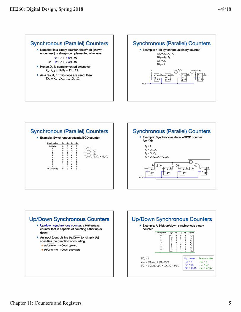
Synchronous (Parallel) Counters§ Note that in a binary counter, the nth bit (shown
underlined) is always complemented whenever011…11 ® 100…00
or 111…11 ® 000…00
§ Hence, Xn is complemented whenever Xn-1Xn-2 ... X1X0 = 11…11.
§ As a result, if T flip-flops are used, then TXn = Xn-1 . Xn-2 . ... . X1 . X0
Synchronous (Parallel) Counters§ Example: 4-bit synchronous binary counter.
TA3 = A2 . A1 . A0
TA2 = A1 . A0
TA1 = A0
TA0 = 1
1
K
J
K
J A1A0
CC
CLK
Q
Q'
Q
Q'
Q
Q' K
J A2
CQ
Q' K
J A3
CQ
Q'
A1.A0 A2.A1.A0
Synchronous (Parallel) Counters§ Example: Synchronous decade/BCD counter.
Clock pulse Q3 Q2 Q1 Q0
Initially 0 0 0 01 0 0 0 12 0 0 1 03 0 0 1 14 0 1 0 05 0 1 0 16 0 1 1 07 0 1 1 18 1 0 0 09 1 0 0 1
10 (recycle) 0 0 0 0
T0 = 1T1 = Q3'.Q0T2 = Q1.Q0T3 = Q2.Q1.Q0 + Q3.Q0
Synchronous (Parallel) Counters§ Example: Synchronous decade/BCD counter
(cont’d).
T0 = 1T1 = Q3'.Q0
T2 = Q1.Q0
T3 = Q2.Q1.Q0 + Q3.Q0
1 Q1
Q0
CLK
TCQ
Q'
Q
Q'
Q2 Q3TCQ
Q'
Q
Q'
TCQ
Q'
Q
Q'
TCQ
Q'
Q
Q'
Up/Down Synchronous Counters§ Up/down synchronous counter: a bidirectional
counter that is capable of counting either up or down.
§ An input (control) line Up/Down (or simply Up) specifies the direction of counting.v Up/Down = 1 ® Count upwardv Up/Down = 0 ® Count downward
Up/Down Synchronous Counters§ Example: A 3-bit up/down synchronous binary
counter.Clock pulse Up Q2 Q1 Q0 Down
0 0 0 01 0 0 12 0 1 03 0 1 14 1 0 05 1 0 16 1 1 07 1 1 1
TQ0 = 1TQ1 = (Q0.Up) + (Q0'.Up' )TQ2 = ( Q0.Q1.Up ) + (Q0'. Q1'. Up' )
Up counterTQ0 = 1TQ1 = Q0
TQ2 = Q0.Q1
Down counterTQ0 = 1TQ1 = Q0’TQ2 = Q0’.Q1’

EE260: Digital Design, Spring 2018 4/8/18
Chapter 11: Counters and Registers 6
Up/Down Synchronous Counters§ Example: A 3-bit up/down synchronous binary
counter (cont’d).TQ0 = 1TQ1 = (Q0.Up) + (Q0'.Up' )TQ2 = ( Q0.Q1.Up ) + (Q0'. Q1'. Up' )
1
Q1Q0
CLK
TCQ
Q'
Q
Q'
TCQ
Q'
Q
Q'
TCQ
Q'
Q
Q'Up
Q2
Designing Synchronous Counters§ Covered in Lecture #12.§ Example: A 3-bit Gray code
counter (using JK flip-flops).
100000
001
101
111110
011
010
Present Next Flip-flopstate state inputs
Q2 Q1 Q0 Q2+ Q1+ Q0+ JQ2 KQ2 JQ1 KQ1 JQ0 KQ00 0 0 0 0 1 0 X 0 X 1 X0 0 1 0 1 1 0 X 1 X X 00 1 0 1 1 0 1 X X 0 0 X0 1 1 0 1 0 0 X X 0 X 11 0 0 0 0 0 X 1 0 X 0 X1 0 1 1 0 0 X 0 0 X X 11 1 0 1 1 1 X 0 X 0 1 X1 1 1 1 0 1 X 0 X 1 X 0
Designing Synchronous Counters§ 3-bit Gray code counter: flip-flop inputs.
0
1
00 01 11 10Q2Q1Q0
X X X X1
JQ2 = Q1.Q0'
0
1
00 01 11 10Q2Q1Q0
X X X X1
KQ2 = Q1'.Q0'
0
1
00 01 11 10Q2Q1Q0
X XX X1
JQ1 = Q2'.Q0
0
1
00 01 11 10Q2Q1Q0
X XX X
1
KQ1 = Q2.Q0
0
1
00 01 11 10Q2Q1Q0
XXXX1
JQ0 = Q2.Q1 + Q2'.Q1'= (Q2 Å Q1)'
1
0
1
00 01 11 10Q2Q1Q0
XXXX 1
1
KQ0 = Q2.Q1' + Q2'.Q1= Q2 Å Q1
Designing Synchronous Counters§ 3-bit Gray code counter: logic diagram.
JQ2 = Q1.Q0' JQ1 = Q2'.Q0 JQ0 = (Q2 Å Q1)'KQ2 = Q1'.Q0' KQ1 = Q2.Q0 KQ0 = Q2 Å Q1
Q1Q0
CLK
Q2J
C
Q
Q'K
J
C
Q
Q'K
J
C
Q
Q'KQ2'
Q0'
Q1'
Decoding A Counter§ Decoding a counter involves determining which
state in the sequence the counter is in.§ Differentiate between active-HIGH and active-LOW
decoding.§ Active-HIGH decoding: output HIGH if the counter is
in the state concerned.§ Active-LOW decoding: output LOW if the counter is
in the state concerned.
Decoding A Counter§ Example: MOD-8 ripple counter (active-HIGH
decoding).
A'B'C'
1 2 3 4 5 6 7 8 9Clock
HIGH only on count of ABC = 000
A'B'C
HIGH only on count of ABC = 001
A'BC'
HIGH only on count of ABC = 010
100
ABC
HIGH only on count of ABC = 111
...

EE260: Digital Design, Spring 2018 4/8/18
Chapter 11: Counters and Registers 7
Decoding A Counter§ Example: To detect that a MOD-8 counter is in state
0 (000) or state 1 (001).
A'B'
1 2 3 4 5 6 7 8 9Clock
HIGH only on count of ABC = 000 or ABC = 001
100
§ Example: To detect that a MOD-8 counter is in the odd states (states 1, 3, 5 or 7), simply use C.
C
1 2 3 4 5 6 7 8 9Clock
HIGH only on count of odd states
100
A'B'C'A'B'C
Counters with Parallel Load§ Counters could be augmented with
parallel load capability for the following purposes:vTo start at a different statevTo count a different sequencevAs more sophisticated register with
increment/decrement functionality.
Counters with Parallel Load§ Different ways of getting a MOD-6 counter:
Count = 1Load = 0CPI4 I3 I2 I1
Count = 1Clear = 1CP
A4 A3 A2 A1
Inputs = 0
Load
(a) Binary states 0,1,2,3,4,5.
I4 I3 I2 I1
A4 A3 A2 A1
Inputs have no effect
Clear
(b) Binary states 0,1,2,3,4,5.
I4 I3 I2 I1
Count = 1Clear = 1CP
A4 A3 A2 A1
0 0 1 1
Load
(d) Binary states 3,4,5,6,7,8.
I4 I3 I2 I1
Count = 1Clear = 1CP
A4 A3 A2 A1
1 0 1 0
Load
Carry-out
(c) Binary states 10,11,12,13,14,15.
Counters with Parallel Load§ 4-bit counter with
parallel load.Clear CP Load Count Function
0 X X X Clear to 01 X 0 0 No change1 1 X Load inputs1 0 1 Next state
Introduction: Registers§ An n-bit register has a group of n flip-flops
and some logic gates and is capable of storing n bits of information.
§ The flip-flops store the information while the gates control when and how new information is transferred into the register.
§ Some functions of register:v retrieve data from registervstore/load new data into register (serial or parallel)vshift the data within register (left or right)
Simple Registers§ No external gates.§ Example: A 4-bit register. A new 4-bit data is
loaded every clock cycle.
A3
CP
A1 A0
DQ
DQ Q
D
A2
DQ
I3 I1 I0I2

EE260: Digital Design, Spring 2018 4/8/18
Chapter 11: Counters and Registers 8
Registers With Parallel Load§ Instead of loading the register at every clock
pulse, we may want to control when to load.§ Loading a register: transfer new information
into the register. Requires a load control input.
§ Parallel loading: all bits are loaded simultaneously.
Registers With Parallel Load
A0
CLK
D Q
Load
I0
A1D Q
A2D Q
A3D Q
CLEAR
I1
I2
I3
Load'.A0 + Load. I0
Using Registers to implement Sequential Circuits
§ A sequential circuit may consist of a register(memory) and a combinational circuit.
Register Combin-ational circuit
Clock
Inputs Outputs
Next-state value
§ The external inputs and present states of the register determine the next states of the register and the external outputs, through the combinational circuit.
§ The combinational circuit may be implemented by any of the methods covered in MSI components and Programmable Logic Devices.
Using Registers to implement Sequential Circuits
§ Example 1:A1
+ = S m(4,6) = A1.x'A2
+ = S m(1,2,5,6) = A2.x' + A2'.x = A2 Å xy = S m(3,7) = A2.x
Present Nextstate Input State OutputA1 A2 x A1+ A2+ y0 0 0 0 0 00 0 1 0 1 00 1 0 0 1 00 1 1 0 0 11 0 0 1 0 01 0 1 0 1 01 1 0 1 1 01 1 1 0 0 1
A1A2
x y
A1.x'
A2Åx
Using Registers to implement Sequential Circuits
§ Example 2: Repeat example 1, but use a ROM.
Address Outputs1 2 3 1 2 30 0 0 0 0 00 0 1 0 1 00 1 0 0 1 00 1 1 0 0 11 0 0 1 0 01 0 1 0 1 01 1 0 1 1 01 1 1 0 0 1
ROM truth table
A1
A2
x y
8 x 3 ROM
Shift Registers§ Another function of a register, besides
storage, is to provide for data movements.§ Each stage (flip-flop) in a shift register
represents one bit of storage, and the shifting capability of a register permits the movement of data from stage to stage within the register, or into or out of the register upon application of clock pulses.

EE260: Digital Design, Spring 2018 4/8/18
Chapter 11: Counters and Registers 9
Shift Registers§ Basic data movement in shift registers (four
bits are used for illustration).Data in Data out
(a) Serial in/shift right/serial out
Data inData out
(b) Serial in/shift left/serial out
Data in
Data out
(c) Parallel in/serial outData out
Data in
(d) Serial in/parallel outData out
Data in
(e) Parallel in / parallel out
(f) Rotate right (g) Rotate left
Serial In/Serial Out Shift Registers§ Accepts data serially – one bit at a time
– and also produces output serially.
Q0
CLK
D
C
QQ1 Q2 Q3Serial data
inputSerial data outputD
C
Q D
C
Q D
C
Q
Serial In/Serial Out Shift Registers§ Application: Serial transfer of data from one
register to another.
Shift register A Shift register BSI SISO SO
ClockShift control
CP
Wordtime
T1 T2 T3 T4CP
Clock
Shift control
Serial In/Serial Out Shift Registers§ Serial-transfer example.
Timing Pulse Shift register A Shift register B Serial output of BInitial value 1 0 1 1 0 0 1 0 0
After T1 1 1 0 1 1 0 0 1 1After T2 1 1 1 0 1 1 0 0 0After T3 0 1 1 1 0 1 1 0 0After T4 1 0 1 1 1 0 1 1 1
Serial In/Parallel Out Shift Registers§ Accepts data serially.§ Outputs of all stages are available simultaneously.
Q0
CLK
D
C
Q
Q1
D
C
Q
Q2
D
C
Q
Q3
D
C
QData input
DCCLK
Data input
Q0Q1Q2Q3
SRG 4Logic symbol
Parallel In/Serial Out Shift Registers§ Bits are entered simultaneously, but output
is serial.D0
CLK
D
C
Q
D1
D
C
Q
D2
D
C
Q
D3
D
C
Q
Data input
Q0 Q1 Q2 Q3
Serial data out
SHIFT/LOAD
SHIFT.Q0 + SHIFT'.D1
EE260: Digital Design, Spring 2018 4/8/18
Chapter 11: Counters and Registers 10
Parallel In/Serial Out Shift Registers§ Bits are entered simultaneously, but output
is serial.
Logic symbol
CCLKSHIFT/LOAD
D0D1D2D3
SRG 4Serial data out
Data in
Parallel In/Parallel Out Shift Registers
§ Simultaneous input and output of all data bits.
Q0
CLK
D
C
Q
Q1
D
C
Q
Q2
D
C
Q
Q3
D
C
Q
Parallel data inputs
D0 D1 D2 D3
Parallel data outputs
Bidirectional Shift Registers§ Data can be shifted either left or right, using a
control line RIGHT/LEFT (or simply RIGHT) to indicate the direction.
CLK
D
C
Q D
C
Q D
C
Q D
C
Q
Q0
Q1 Q2Q3
RIGHT/LEFT
Serial data in
RIGHT.Q0 + RIGHT'.Q2
Bidirectional Shift Registers§ 4-bit bidirectional shift register with parallel
load.
CLK
I4 I3 I2 I1
Serial input for shift-right
DQ
DQ
DQ
DQClear
4x1 MUX
s1
s03 2 1 0
4x1 MUX
3 2 1 0
4x1 MUX
3 2 1 0
4x1 MUX
3 2 1 0
A4 A3 A2 A1
Serial input for shift-left
Parallel inputs
Parallel outputs
Bidirectional Shift Registers§ 4-bit bidirectional shift register with parallel
load.Mode Controls1 s0 Register Operation0 0 No change0 1 Shift right1 0 Shift left1 1 Parallel load
An Application – Serial Addition§ Most operations in digital computers are done in
parallel. Serial operations are slower but require less equipment.
§ A serial adder is shown below. A ¬ A + B.
FAxyz
SC
Shift-register AShift-rightCP
SI
Shift-register B
SIExternal input SO
SO
Q D
Clear
EE260: Digital Design, Spring 2018 4/8/18
Chapter 11: Counters and Registers 11
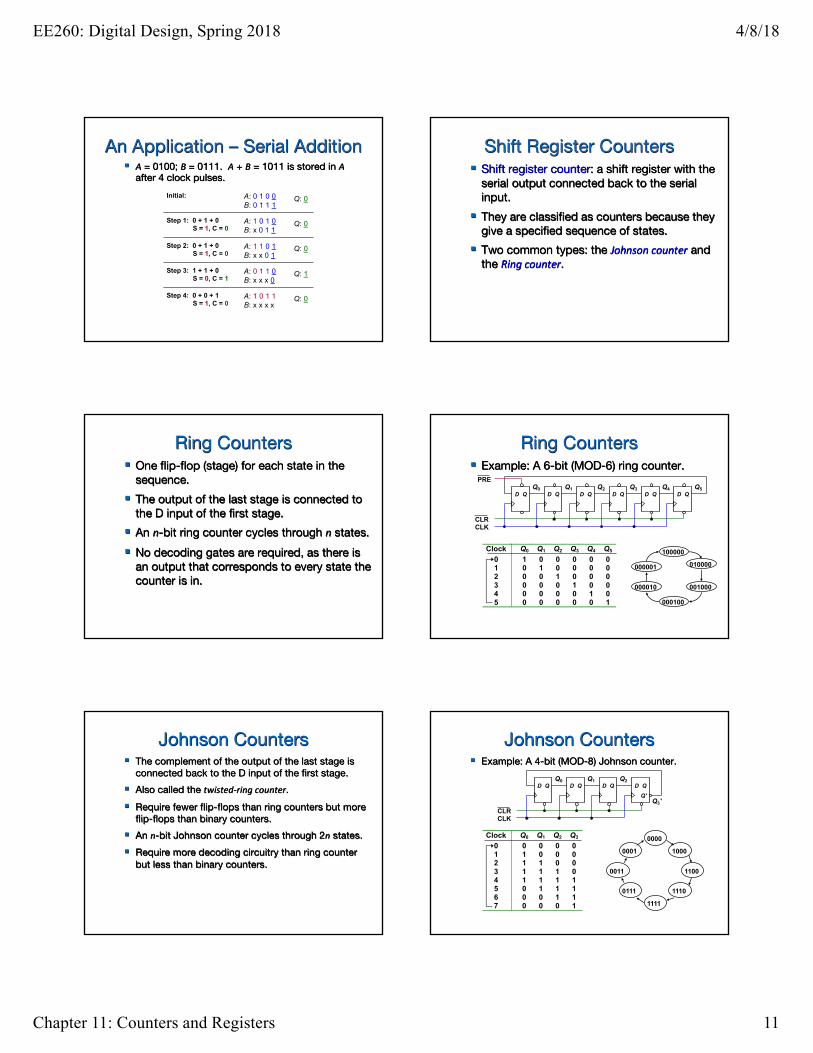
An Application – Serial Addition§ A = 0100; B = 0111. A + B = 1011 is stored in A
after 4 clock pulses. Initial: A: 0 1 0 0
B: 0 1 1 1Q: 0
Step 1: 0 + 1 + 0S = 1, C = 0
A: 1 0 1 0B: x 0 1 1
Q: 0
Step 2: 0 + 1 + 0S = 1, C = 0
A: 1 1 0 1B: x x 0 1
Q: 0
Step 3: 1 + 1 + 0S = 0, C = 1
A: 0 1 1 0B: x x x 0
Q: 1
Step 4: 0 + 0 + 1S = 1, C = 0
A: 1 0 1 1B: x x x x
Q: 0
Shift Register Counters§ Shift register counter: a shift register with the
serial output connected back to the serial input.
§ They are classified as counters because they give a specified sequence of states.
§ Two common types: the Johnson counter and the Ring counter.
Ring Counters§ One flip-flop (stage) for each state in the
sequence.§ The output of the last stage is connected to
the D input of the first stage.§ An n-bit ring counter cycles through n states.§ No decoding gates are required, as there is
an output that corresponds to every state the counter is in.
Ring Counters§ Example: A 6-bit (MOD-6) ring counter.
CLK
Q0D Q D Q D Q D Q D Q D Q
Q1 Q2 Q3 Q4 Q5
CLR
PRE
Clock Q0 Q1 Q2 Q3 Q4 Q50 1 0 0 0 0 01 0 1 0 0 0 02 0 0 1 0 0 03 0 0 0 1 0 04 0 0 0 0 1 05 0 0 0 0 0 1
100000
010000
001000
000100
000010
000001
Johnson Counters§ The complement of the output of the last stage is
connected back to the D input of the first stage.§ Also called the twisted-ring counter.§ Require fewer flip-flops than ring counters but more
flip-flops than binary counters.§ An n-bit Johnson counter cycles through 2n states.§ Require more decoding circuitry than ring counter
but less than binary counters.
Johnson Counters§ Example: A 4-bit (MOD-8) Johnson counter.
Clock Q0 Q1 Q2 Q30 0 0 0 01 1 0 0 02 1 1 0 03 1 1 1 04 1 1 1 15 0 1 1 16 0 0 1 17 0 0 0 1
CLK
Q0D Q D Q D Q D Q
Q1 Q2
Q3'CLR
Q'
0000
0001
0011
0111
1111
1110
1100
1000

EE260: Digital Design, Spring 2018 4/8/18
Chapter 11: Counters and Registers 12
Johnson Counters§ Decoding logic for a 4-bit Johnson counter.
Clock A B C D Decoding0 0 0 0 0 A'.D'1 1 0 0 0 A.B'2 1 1 0 0 B.C'3 1 1 1 0 C.D'4 1 1 1 1 A.D5 0 1 1 1 A'.B6 0 0 1 1 B'.C7 0 0 0 1 C'.D
A'D' State 0
AD State 4
BC' State 2
CD' State 3
AB' State 1
A'B State 5
B'C State 6
C'D State 7
Random Access Memory (RAM)§ A memory unit stores binary information in groups of
bits called words.§ The data consists of n lines (for n-bit words). Data
input lines provide the information to be stored (written) into the memory, while data output linescarry the information out (read) from the memory.
§ The address consists of k lines which specify which word (among the 2k words available) to be selected for reading or writing.
§ The control lines Read and Write (usually combined into a single control line Read/Write) specifies the direction of transfer of the data.
Random Access Memory (RAM)§ Block diagram of a memory unit:
Memory unit2k wordsn bits per word
k address linesk
Read/Write
n
n
n data input lines
n data output lines
Random Access Memory (RAM)§ Content of a 1024 x 16-bit memory:
101101011101110110100001100001100010011101110001::111001010101001000111110101011101011000110010101
Memory contentdecimal
012::
102110221023
000000000000000000010000000010
::
111111110111111111101111111111
binaryMemory address
Random Access Memory (RAM)§ The Write operation:
v Transfers the address of the desired word to the address lines
v Transfers the data bits (the word) to be stored in memory to the data input lines
v Activates the Write control line (set Read/Write to 0)
§ The Read operation:v Transfers the address of the desired word to the address
linesv Activates the Read control line (set Read/Write to 1)
Random Access Memory (RAM)§ The Read/Write operation:
Memory Enable Read/Write Memory Operation0 X None1 0 Write to selected word1 1 Read from selected word
§ Two types of RAM: Static and dynamic.§ Static RAMs use flip-flops as the memory cells.§ Dynamic RAMs use capacitor charges to represent
data. Though simpler in circuitry, they have to be constantly refreshed.

EE260: Digital Design, Spring 2018 4/8/18
Chapter 11: Counters and Registers 13
Random Access Memory (RAM)§ A single memory cell of the static RAM has
the following logic and block diagrams.
R
S QInput
Select
Output
Read/Write
BC OutputInput
Select
Read/Write
Logic diagram Block diagram
Random Access Memory (RAM)§ Logic construction of a 4 x 3 RAM (with decoder and
OR gates):
Random Access Memory (RAM)§ An array of RAM chips: memory chips are combined
to form larger memory.§ A 1K x 8-bit RAM chip:
Block diagram of a 1K x 8 RAM chip
RAM 1K x 8
DATA (8)ADRS (10)CSRW
Input dataAddress
Chip selectRead/write
(8) Output data8 810
Random Access Memory (RAM)
§ 4K x 8 RAM.
1K x 8
DATA (8)ADRS (10)CSRW
Read/write
(8)
Output data
1K x 8
DATA (8)ADRS (10)CSRW
(8)
1K x 8
DATA (8)ADRS (10)CSRW
(8)
1K x 8
DATA (8)ADRS (10)CSRW
(8)
0–1023
1024 – 2047
2048 – 3071
3072 – 4095
Input data8 lines
0123
2x4 decoder
Lines Lines0 – 911 10
S0
S1
Address