Estimation of Delay, Power, And Bandwidth for on-Chip VLSI Global Interconnects

1
VLSI Design for Multi-Sensor Smart Systems on a Chip
Louiza Sellami1 and Robert W. Newcomb2 1Electrical and Computer Engineering Department,
US Naval Academy, Annapolis, MD 2Electrical and Computer Engineering Department,
University of Maryland, College Park, MD USA
1. Introduction
Sensors are becoming of considerable importance in several areas, particularly in healthcare. Therefore, the development of inexpensive and miniaturized sensors that are highly selective and sensitive, and for which control and analysis is present all on one chip is very desirable. These types of sensors can be implemented with micro-electro-mechanical systems (MEMS), and because they are fabricated on a semiconductor substrate, additional signal processing circuitry can easily be integrated into the chip, thereby readily providing additional functions, such as multiplexing and analog-to-digital conversion. Here we present a general framework for the design of a multi-sensor system on a chip, which includes intelligent signal processing, as well as a built-in self test and parameter adjustment units. Specifically, we outline the system architecture, and develop a transistorized bridge biosensor for monitoring changes in the dielectric constant of a fluid, which could be used for in-home monitoring of kidney function of patients with renal failure.
In a number of areas it would be useful to have available smart sensors which can determine the properties of a fluid and from those make a reasoned decision. Among such areas of interest might be ecology, food processing, and health care. For example, in ecology it is important to preserve the quality of water for which a number of parameters are of importance, including physical properties such as color, odor, PH, as well as up to 40 inorganic chemical properties and numerous organic ones (DeZuane, 1990). Therefore, in order to determine the quality of water it would be extremely useful if there were a single system on a chip which could be used in the field to measure the large number of parameters of importance and make a judgment as to the safety of the water. For such, a large number of sensors is needed and a means of coordinating the readouts of the sensors into a user friendly output from which human decisions could be made. As another example, the food processing industry needs sensors to tell if various standards of safety are met. In this case it is important to measure the various properties of the food, for example the viscosity and thermal conductivity of cream or olive oil (Singht & Helman, 1984).
www.intechopen.com

VLSI Design 4
In biomedical engineering, biosensors are becoming of considerable importance. General
theories of different types of biosensors can be found in (Van der Shoot & Berveld, 1988;
Eggins, 1996; Scheller & Schubert,1992) while similar devices dependent upon temperature
sensing are introduced in (Herwarden et al, 1994). Methods for the selective determination
of compounds in fluids, such as blood, urine, and saliva, are indeed very important in
clinical analysis. Present methods often require a long reaction time and involve
complicated and delicate procedures. One valuable application in the health care area is that
of the use of multiple sensors for maintaining the health of astronauts where presently an
array of eleven sensors is used to maintain the quality of recycled air (Turner et al, 1987),
although separate control is effected by the use of an external computer. Therefore, it is
desirable to develop inexpensive and miniaturized sensors that are highly selective and
sensitive, and for which control and analysis is available all on the same chip. These sensors
can be implemented with micro-electro-mechanical systems (MEMS). Since they are
fabricated on a semiconductor substrate, additional signal processing units can easily be
integrated into the chip thereby readily providing functions such as multiplexing and
analog-to-digital conversion. In numerous other areas one could find similar uses for a
smart multi-sensor array from which easy measurements can be made with a small portable
device. These are the types of systems on a chip (SOC) that this chapter addresses.
2. System on a chip architecture
The architecture of these systems is given in Fig. 2.1 where there are multiple inputs, sensors, and outputs. In between are smart signal processing elements including built-in self-test (BIST). In this system there may be many classes of input signals (for example, material [as a fluid] and user [as indicator of what to measure]). On each of the inputs there may be many sensors (for example, one material may go to several sensors each of which
Fig. 2.1. Architecture for N-Sensor Smart System on a Chip
N -S e n so r S m a rt S ys te m o n a C h ip
S e n so r 1
S e n so r 2
S e n so r N
In te l l ig e n t
P re p ro c e ss in g
A m p l if ie rs
S ig n a l M ixin g
M ixe d & In te l l ig e n t
S ig n a l
P ro c e ss in g
A /D
M ic ro p ro c e ss in g
D S P
N e u ra l N e tw o rk
B u il t- In S e lf T e s t a n d P a ra m e te r A d ju s tm e n ts
O u tp u tsIn p u ts
www.intechopen.com
VLSI Design for Multi-Sensor Smart Systems on a Chip 5
senses a different property [as dielectric constant in one and resistivity in another]). The sensor signals are treated as an N-vector and combined as necessary to obtain the desired outputs, of which there may be many (such as an alarm for danger and indicators for different properties). For example, a patient with kidney disease may desire a system on a chip which gives an indication of when to report to the hospital. For this an indication of deviation of dielectric constant from normal and spectral properties of peritonal fluid may be sensed and combined to give the presence of creatinine (a protein produced by the muscles and released in the blood) in the fluid, with the signal output being the percent of creatinine in the fluid and an alarm when at a dangerous level.
3. Dielectric constant and resistivity sensor
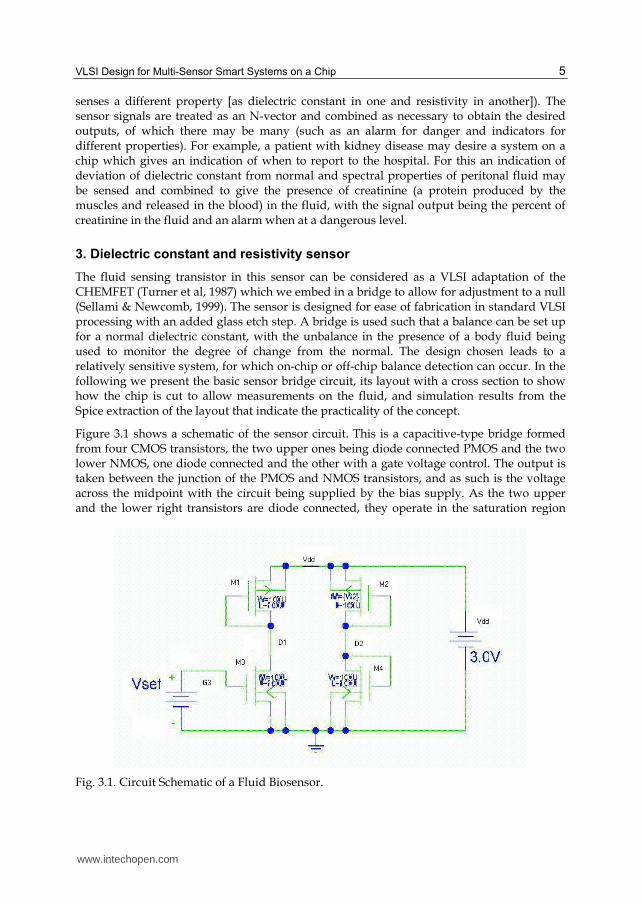
The fluid sensing transistor in this sensor can be considered as a VLSI adaptation of the CHEMFET (Turner et al, 1987) which we embed in a bridge to allow for adjustment to a null (Sellami & Newcomb, 1999). The sensor is designed for ease of fabrication in standard VLSI processing with an added glass etch step. A bridge is used such that a balance can be set up for a normal dielectric constant, with the unbalance in the presence of a body fluid being used to monitor the degree of change from the normal. The design chosen leads to a relatively sensitive system, for which on-chip or off-chip balance detection can occur. In the following we present the basic sensor bridge circuit, its layout with a cross section to show how the chip is cut to allow measurements on the fluid, and simulation results from the Spice extraction of the layout that indicate the practicality of the concept.
Figure 3.1 shows a schematic of the sensor circuit. This is a capacitive-type bridge formed from four CMOS transistors, the two upper ones being diode connected PMOS and the two lower NMOS, one diode connected and the other with a gate voltage control. The output is taken between the junction of the PMOS and NMOS transistors, and as such is the voltage across the midpoint with the circuit being supplied by the bias supply. As the two upper and the lower right transistors are diode connected, they operate in the saturation region
Fig. 3.1. Circuit Schematic of a Fluid Biosensor.
www.intechopen.com

VLSI Design 6
while the gate (the set node) of the lower left transistor, M3, is fed by a variable DC supply allowing that transistor to be adjusted to bring the bridge into balance. The upper right transistor, M2, has cuts in its gate to allow fluid to enter between the silicon substrate and the polysilicon gate. In so doing the fluid acts as the gate dielectric for that transistor. Because the dielectric constants of most fluids are a fraction of that of silicon dioxide, the fraction for water being about 1/4, M2 is actually constructed out of several transistors, four in the case of water, with all of their terminals (source, gate, drain) in parallel to effectively multiply the Spice gain constant parameter KP which is proportional to the dielectric constant.
The sensor relies upon etching out much of the silicon dioxide gate dielectric. This can be accomplished by opening holes in protective layers by using the overglass cut available in MEMS fabrications. Since, in the MOSIS processing that is readily available, these cuts should be over an n-well, the transistor in which the fluid is placed is chosen as a PMOS one. And, since we desire to maintain a gate, only portions are cut open so that a silicon dioxide etch can be used to clear out portions of the gate oxide, leaving the remaining portions for mechanical support. To assist the mechanical support we also add two layers of metal, metal-1 and metal-2, over the polysilicon gate.
A preliminary layout of the basic sensor is shown in Fig. 3.2 for M2 constructed from four subtransistors, this layout having been obtained using the MAGIC layout program. As the latter can be used with different lambda values to allow for different technology sizes, this layout can be used for different technologies and thus should be suitable for fabrications presently supported by MOSIS. Associated with Fig. 3.2 is Fig. 3.3 where a cross section is shown cut through the upper two transistors in the location seen on the upper half of the figure. The section shows that the material over the holes in the gate is completely cut away so that an etching of the silicon dioxide can proceed to cut horizontally under the remaining portions of the gate. The two layers of metal can also be seen as adding mechanical support to maintain the cantilevered portions of the gate remaining after the silicon dioxide etch.
Fig. 3.2. Biosensor VLSI Layout
www.intechopen.com

VLSI Design for Multi-Sensor Smart Systems on a Chip 7
Fig. 3.3. Cross Section of Upper Transistors
To study the operation of the sensor we turn to the describing equations. Under the valid
assumption that no current is externally drawn from the sensor, the drain currents of M1
and M3 are equal and opposite, ID3=-ID1, and similarly for M2 and M4, ID4=-ID2. Assuming
that all transistors are operating above threshold, since M1, M3, and M4 are in saturation
they follow a square law relationship while the law for M3 we designate through a function
f(Vset,VD1) which is controlled by Vset. Thus,
-ID1 = 1(Vdd-VD1-|Vthp|)2(1+p[Vdd-VD2]) (3.1a)
= 3[f(Vset,VD1)(1+nVD1) = ID3 (3.1b)
-ID2 = 2(Vdd-VD2-|Vthp|)2(1+p[Vdd-VD2]) (3.2a)
= 4(VD2-Vthn)2(1+nVD2) = ID4 (3.2b)
where, for the ith transistor,
i = KPiWi/2Li, i=1,2,3,4 (3.3)
and
f(x,y) = {(x-Vthn)2 if x-Vthn<y, 2(x-Vthn)y-y2 if x-Vthn y} (3.4)
Here Vth, KP, and are Spice parameters for silicon transistors, all constants in this case, with the n or p denoting the NMOS or PMOS case, and epsilon is the ratio of the dielectric constant of the fluid to that of silicon dioxide,
=fluid /Sio2. (3.5)
In order to keep the threshold voltages constant we have tied the source nodes to the bulk material in the layout. In our layout we also choose the widths and lengths of M1, M3, and
M4 to be all equal to 100 and L2/W2 to approximate . Under the reasonable assumption
that the 's are negligibly small, an analytic solution for the necessary Vset to obtain a balance can be obtained. When M3 is in saturation the solution is
www.intechopen.com

VLSI Design 8
VD1 = Vdd-|Vthp|-(3/1}1/2(Vset-Vthn) (3.6)
while irrespective of the state of M3
VD2={Vthn+(.2/4)1/2(Vdd-|Vthp|)/[1+.2/4]1/2} (3.7)
Fig. 3.4. Extracted circuit output voltage versus Vset
Balance is obtained by setting VD1=VD2. Still assuming that M3 is in saturation the value of Vset needed to obtain balance is obtained from equations (3.6) and (3.7) as
Vset=Vthn+{(1/3})1/2(Vdd-|Vthp|-Vthn)/[1+(.2/4})1/2} (3.8)
At this point we can check the condition for M3 to be in saturation, this being that VDS
VGS-Vthn; since VDS=VD1 and VGS = Vset, the use of Equation (3.6) gives
Vthn < Vset{sat} Vthn+(Vdd-|Vthp|)/[1+(3/1)1/2 ] (3.9)
Substituting the value of Vset at balance, Equation (3.8), shows that the condition for M3 to be in saturation at balance is 2 3; this normally would be satisfied but can be guaranteed by making M2 large enough.
Several things are added to the sensor itself per Fig. 2.1. Among these is a differential pair for direct current mode readout followed by a current mode pulse coded neural network to do smart preprocessing to insure the integrity of the signals. Finally a built in test circuit is included to detect any breakdown in the sensor operation.
From the layout of Fig. 3.1 a Spice extraction was obtained. On incorporating the BiCMOSIS transistor models (Sellami & Newcomb, 1999; Moskowtitz et al, 1999) the extracted circuit file was run in PSpice with the result for the output difference voltage versus Vset shown in Fig. 3.4. As can be seen, adjustment can be made over the wide range of -5V<Vset<5V
Thus, it is seen that a sensor that is sensitive to the dielectric constant of a fluid over an 11 to 1 range of dielectric constant most likely can be incorporated into a multi-sensor chip. Using standard analog VLSI-MEMS processing one can use the bridge for anomalies in a fluid by obtaining Vset for the normal situation and then comparing with Vset found for the
www.intechopen.com

VLSI Design for Multi-Sensor Smart Systems on a Chip 9
anomalous situation. This could be particularly useful for determining progress of various diseases. For example, one way to determine kidney function and dialysis adequacy is through the clearance test of creatinine. The latter tests for the amount of blood that is cleared of creatinine per time period, which is usually expressed in ml per minute. For a healthy adult the creatinine clearance is 120 ml/min.
A renal adult patient will need dialysis because symptoms of kidney failure appear at a clearance of less than 10 ml/min. Creatinine clearance is measured by urine collection, usually 12 or 24 hours. Therefore a possible use for the proposed sensor could be as a creatinine biosensor device for individual patient to monitor the creatinine level at home. An alternate to the proposed biosensor is based on biologically sensitive coatings, often enzymes, which could be used on M2 transistor in a technology that is used for urea biosensors which are presently marketed for end stage renal disease patients (Eggins, 1996). The advantage of the sensor presented here is that it should be able to be used repetitively whereas enzyme based coatings have a relatively short life. The same philosophy of a balanced bridge constructed in standard VLSI processing can be carried over to the measurement of resistivity of a fluid. In this case the bridge will be constructed of three VLSI resistors with the fourth arm having a fluid channel in which the conductance of the fluid is measured.
4. Spectral sensors
We take advantage of the developments in MEMS technologies to introduce new and improved methodology and engineering capabilities in the field of chemical and biochemical optical sensors for the analysis of a fluid. The proposed device has the advantages of size reduction and, therefore, increased availability, reduced consumption of chemical/biochemical sample, compatibility with other MEMS technologies, and integrability with computational circuitry on the chip.
Consequently, integrating MEMS and optical devices will give the added advantages of size reduction and integrability with the electrical circuitry. The integration and compatibility of sensors is very much in demand in the field of system on a chip. Here we extend CMOS technology to build an optical filter which can be used in a single chip microspectrometer. The chip contains an array of microspectrometer and photodetectors and the read out of their circuits.
By the nature of matter in the universe, most evident at the atomic and molecular level, it allows so much information to be deduced from its optical spectra. Because molecule and atoms can only emit or absorb photons with energies that correspond to certain allowed transition between quantum states, optical spectroscopy is one of the valuable tools of analytical chemistry (Schmidt, 2005). Optically based chemical and biological sensors are conveniently classified into five groups, according to the way light is modulated (Ellis, 2005). These light modulations are intensity, wavelength, polarization, phase, and time modulation. Here we focus on MEMS based sensors suitable for Intensity, wavelength, and time modulation.
4.1 Intensity modulation
As light passes through a material, its intensity attenuates as it interacts with the molecules, atoms, and impurities of the host material. The attenuation is an exponential function of the
www.intechopen.com

VLSI Design 10
distance of its path length, x, traveled in the material. The absorption coefficient, , is defined relative to the concentration, M, and the cross section, S, of the absorbing molecules (Svanberg, 2001).
I(x) = I(0) . exp (.x) = I(0) . exp (-S.MxN) (4.1.1)
Where I(x) is the light intensity at distance x, I(0) the incident light intensity at x = 0, and N Avogado’s number (6.022 x 10²³ mol-1).
Changes of the analyte concentration in the sample can alter the absorption coefficient . An absorption based sensor measures these changes by the transmitted light intensity in terms of absorbance (A) units:
A = log[I(0)/ I(x)] (4.1.2)
4.2 Wavelength modulation
Wavelength modulation can provide us with more information than just the intensity modulation. Several numbers of fixed wavelength sources are used simultaneously and their responses, intensity, are detected using photo detectors. Several sources that are modulated at different electrical frequencies can be used simultaneously in order to use a single photo detector. One of the wavelengths could serve as a reference channel for calibration.
Fluorescence occurs when an atom or a molecule makes a transition from a higher energy state to a lower one and emits lights. Excitation and subsequent emission can occur not only by photoluminescence but also by chemical reaction (chemiluminescence) or biological reaction (Bioluminescence). In resonance fluorescence, absorption and emission take place between the same two energy levels, and therefore the wavelength of the excitation and emission lights are the same. In non-resonant fluorescence, emission occurs either at higher wavelength than excitation wavelength (Stokes Fluorescence), or lower wavelength than excitation wavelength (anti- Stokes Fluorescence). The decay rate dN/dt of the fluorescence for a two level system is
dN/dt = -kt . N (4.2.1)
where kt is the total fluorescence rate, in sec-1, and N is proportional to the number of electrons excited due to the fluorescent state in a time t. Hence
N = N0 . exp(-kt . t) (4.2.2)
I(0)
I(x)
log I
Lamda X
(a) Intensity vs. wavelength
Light Source Sample Filter Detector
(b)
Fig. 4.2. (a) Attenuation of the optical intensity as it travels along the x axis throught the matter versus the wavelength. (b) corresponding schematic for measurement.
www.intechopen.com

VLSI Design for Multi-Sensor Smart Systems on a Chip 11
4.3 Time modulation
Time modulation is essentially a subclass of intensity modulation. In time domain fluoremetry (TDF), a pulsed light source generates the photoluminescence. The fluorescence decay signal is measured as a function of time, and the decay curve determines the lifetime of the chemical sample. In time modulation base sensors measure the halftime of the sample.
X
Sample Filter Detec tor
(b )
Puls ed light source
Tim e
In te nsity
Fig. 4.3. (a) Fluorescence decay curve (b) corresponding schematic for measurement
5. MEMS based photo-sensors
An important part of any spectrometer, aside from the light source, is the optical filter and photo detectors. Recent engineering developments in the field of MEMS and microelectronics have shown that both of these devices can be produced in the micro level using existing technology (Hsu, 2008). Optical spectrometers can be produced using a tunable Fabry-Perot cavity (here simply called Fabry-Perot). The band-pass frequency range of the Fabry-Perot is a function of its cavity length (Patterson, 1997).
Fabry-Perot can be fabricated in the CMOS technology with photo-detectors integrated underneath it. In other words, Fabry-Perot is fabricated on top of a p-n diode in the CMOS technology. In this configuration, the p-n photo-detector is acting as a transducer that converts optical intensity of light that is passed through the Fabry-Perot to a proportional electrical signal. The existence of the Fabry-Perot in the optical path causes the photodiode to only respond to the light intensity of selected wavelength, which is set by the thickness of the Fabry-Perot cavity.
As illustrated in Fig. 5.1 below, the fabrication of Fabry-Perot and photodiode (FPPD), which starts with the fabrication of a p-n photo diode in a CMOS process technology, undergoes a post process in order to integrate a planer Fabry-Perot on top of the p-n photo diode. This process involves four steps. First, a portion of the top oxide layer immediately above the p-n diode is trimmed, by chemical itching, to reduce its effect on light
cavity
Ag (silver), 45nm
SiO , 300nm 2
Al (aluminuim), 20nm 450 500 550 700 nm
18 Transmission (%)
Lamda
Fig 5.1. The Fabry-perot etalon with AI bottom Mirror
www.intechopen.com

VLSI Design 12
transmission. Second, a thin Aluminum layer is deposited, to form the lower mirror. Third, a layer of Silicon dioxide is added then etched to different sizes, using several masks. This way, each photodiode will have a different size of SiO2 layer on top of it. Fourth, a thin layer of silver (Ag) is deposited on top of all oxide to form the top mirror layer (Tyree et al, 1994).
N-well
P epilayer
P substrate +
_
p-n diode
P
Oxide
Fig. 5.2. Schematic structure for fabrication of a CMOS p-n photo diodes
N-well
P epilayer
P substrate +
_
p-n diode
P
etch top oxide layer
Fig. 5.3. Post CMOS process, 1st step, trimming the top oxide layer above the diode
N-well
P epilayer
P substrate +
_
p-n diode
P-diffusion
PECVD oxide Aluminum
Silver
Metal 1, 2
Fig. 5.4. Post CMOS process, Step 2nd, 3rd, and 4th. Depositing AL, PECVD oxide, and Silver, respectively, on top of p-n diodes to form Fabry-perot cavity filter
6. Optical micro-chemical and biochemical sensors
Optical sensors can be fabricated as shown in Fig. 6.1. A series of Fabry-Perot of different wavelength is fabricated in series, each having its own p-n photo-detectors, immediately underneath. These photodiodes are optically and electrically isolated from each other to reduce cross interference. A micro channel is fabricated on top of the series of Fabry-Perot photodetectors (FPFD) modules. Of course, FPFD modules can appear in any efficient
www.intechopen.com

VLSI Design for Multi-Sensor Smart Systems on a Chip 13
configuration, such as a matrix format, under the flow channel. The entire structure of micro-channel and their FPFD modules can be fabricated in a twin parallel configuration, as shown in Fig. 6.2. In time modulation, this configuration can be used when one channel is empty and one channel is filled with chemical sample. In this situation, there are two received signals for each wavelength. One is the attenuated signal due to the sample, and the other one is a signal for cross-reference and evaluation of the intensity attenuation due to the chemical sample. This configuration can be also used in measurement of fluorescence. Two different dyes can be introduced in two channels in order to evaluate two different analyte concentrations.
. .
. Series of fabry-perots w ith different cavity s izes
Glasses to form f low channel
Series of p-n photo detectors P
P P
N N
N
Sample f low s in the channel
light sourse
FPPDM
Fig. 6.1. Schematic structure of optical micro sensors using fabry-perot and p-n photo detectors
p N
p N .
. .
p N
p N .
. .
Flow
Fig. 6.2. Two parallel micro flow channels, each with its own FPFD module underneath
www.intechopen.com

VLSI Design 14
An array of FPPD is made of many individual FPPD that have different cavity thickness and therefore different range of pass band frequencies. The thickness of these oxide cavities is changed gradually in order to cover some desired range of the light spectrum. The array of FPPD can be formed in one or several columns, all entirely under the microchannel. Any light source that is transmitted through the micro channels will eventually reach these FPPD array under the channel. Each individual FPPD will react only to a small spectrum band of the light that is passed through its Fabry-Perot. Each individual FPPD is connected to the electronic circuit on the chip that will perform the signal conditioning and final post data processing.
7. Companion electronic circuitry
A block diagram of this circuitry is depicted in Fig. 7. All photodetector p-n diodes in the array of FPPD under the channel produce a current whose magnitude contains information related to light intensity. Furthermore this light intensity, which is absorbed by the photodiodes, depends on the content of the chemicals present in the micro-channel fluid. The main purpose of this electronic circuitry is to collect, condition, and interface these current signals to the post processing circuit. Since the information signals are in the form of diode currents, it is preferred to work with current mode (CM) electronic circuits.
Array of FPPD
Sensors,
Amplifiers,
Interface
Circuitry
Micro
Processor And
ADC
Fig. 7. Companion Electronic circuit connects array of FPPD to the microprocessor
8. Built-In-Self-Test
The Built-In-Self-Test (BIST) can interface with the sensors and other circuits under consideration. It can be built upon modifications of circuits and ideas available in the literature, such as the use of oscillations for mixed signal testing including the production line technique of using standard ring oscillator properties. The BIST is needed due to the fact that there are many interacting subsystems, and an error in one can perhaps drastically affect the operation of others.
BIST circuitry consists of a controller, a pattern generator and a multiple input signature analyzer. The Built-in Self-Test method allows core testing to be realized by commanding the core BIST controller to initiate self test and by knowing what the correct result should be. On-chip testing of embedded memories can be realized by either multiplexing their address and data lines to external SOC I/O pads or by using the core processor to apply enough read/write patterns of various types to ensure the integrity of the memory. This technique
www.intechopen.com

VLSI Design for Multi-Sensor Smart Systems on a Chip 15
works best for small embedded memories. Some recommend providing embedded memories with their own BIST circuitry.
For BIST to be effective, there must be a means for on-chip test response measurement, on-chip test control for digital and analog test, and I/O isolation. There are three categories of measurements that can be distinguished: DC static measurements, AC dynamic measurements, and time domain measurements. The first of these, DC static measurements, includes the determination of the DC operating points, bias and DC offset voltages and DC gain. DC faults can be detected by a single set of steady state inputs. AC dynamic measurements measure the frequency response of the system under test. The input stimulus is usually a sine-wave form with variable frequency. Digital signal processing (DSP) techniques can be employed to perform harmonic spectral analysis. Time domain measurements derive slew rate, rise and delay times using pulse signals, ramps or triangular waveforms as the input stimuli of the circuit.
9. Smart signal processing
This stage consists of a mixed and intelligent DSP system that allows for the following functions to be performed.
Analog-to-digital conversion: provides a signal interface between the sensor outputs (analog) and the signal processor inputs (digital).
Determine fluid properties (physical and chemical): Neural and DSP algorithms as well as circuits can be used to carry out computations of fluid parameters such as dielectric constant, resistivity, spectrum, and chemical composition from the digitized sensor outputs.
Detection and identification: The information obtained in step 2 above is fed to a microprocessor that can identify the chemical composition of the fluid and makes an intelligent decision in relation to the condition that is being monitored (water safe or not for drinking, dialysis needed or not, etc.). This can be readily programmed using look-up tables and threshold levels.
Parameter selection and adjustment: These will be for various situations so as to include function selection to tell the sensor what to measure. In addition, the system must have the capability to compensate for deviations, detected by the built-in self test unit, of parameters such as amplifier gain, and micro-processor and neural circuit weight constants.
10. Summary
In this chapter we developed a general framework for the design and fabrication of a multi-sensor system on a chip, which includes intelligent signal processing, as well as a built-in self test and parameter adjustment units. Further, we outlined its architecture, and examined various types of sensors (fluid biosensors for measuring resistivity and dielectric constant, spectral sensors, MEMS based photo-sensors, and optical micro-chemical and biochemical sensors), and fabrication techniques, as well as develop a transistorized bridge fluid biosensor for monitoring changes in the dielectric constant of a fluid, which could be of use for in-home monitoring of kidney function of patients with renal failure.
www.intechopen.com

VLSI Design 16
11. Acknowledgments
This research was sponsored in part by the 2007 Wertheim Fellowship, US Naval Academy.
12. References
De Zuane, Handbook of Drinking Water Quality, Standards and Control,Van Nostrand Reinhold, New York, 1990.
Eggins, B. R., Biosensors: an Introduction, Wiley-Teubner, New York, 1996. Ellis, A. M., Electronic and Photoelectron Spectroscopy: Fundamentals and Case Studies,
Cambridge University Press, 2005. Herwaarden, A. W. Van, P. M. Sarro, J. W. Gardner, and P. Bataillard, “Liquid and Gas
Micro-calorimeters for (Bio)chemical Measurements,” Sensors and Actuators, Vol. 43, 1994, pp. 24-30.
Hsu, T. R., MEMS and Microsystems: Design, manufacture, and Nanoscale Engineering, John Wiley, 2008.
Moskowitz, M., L. Sellami, R. Newcomb, and V. Rodellar, “Current Mode Realization of Ear-Type Multisensors,” International Symposium on Circuits and Systems, ISCAS 2001, Sydney, Australia, volume 2, pp. 285-289.
Patterson, J. D., “Micro-Mechanical Voltage Tunable Fabry-Perot Filters Formed in (111) Silicon,” National Aeronautics and Space Administration, Langley Research Center, 1997.
Scheller, F., and F. Schubert, Biosensors, Elsevier, Amsterdam, 1992. Schmidt, W., Optical Spectroscopy in Chemistry and Life Sciences, Wiley-VCH, 2005. Sellami, L., and R. W. Newcomb, “A Mosfet Bridge Fluid Biosensor,” IEEE International
Symposium on Circuits and Systems, May 30-June 2, 1999, Vol. V, pp. 140-143. Singth, R. P., and D.R. Heldman, Introduction to Food Engineering,Academic Press, Inc.,
1984. Svanberg, S., Atomic and Molecular Spectroscopy: Basic Aspects and Practical Applications,
Springer, 2001. Turner, A. P. F., I. Karube, and G. S. Wilson, Editors, Biosensors, Fundamentals and
Applications, Oxford University Press, Oxford, 1987. Tyree, V., J.-I. Pi, C. Pina, W. Hansford, J. Marshall, M. Gaitan, M. Zaghloul, and D.
Novotny, “Realizing Suspended Structures on Chips Manufactured by CMOS Foundry Processes through the MOSIS Service,” MEMS Announcement, 41 pages, available [email protected], 1994.
Van der Schoot and P. Berveld, “Use of Immobilized Enzymes in FET-Detectors,” in Analytical Uses of Immobilized Biological Compounds for Detection, Medical and Industrial Uses, edited by G. G. Guilbault and M. Mascini, Reidel Publishing Co., Ultrecht, 1988, pp. 195-206.
www.intechopen.com

VLSI DesignEdited by Dr. Esteban Tlelo-Cuautle
ISBN 978-953-307-884-7Hard cover, 290 pagesPublisher InTechPublished online 20, January, 2012Published in print edition January, 2012
InTech EuropeUniversity Campus STeP Ri Slavka Krautzeka 83/A 51000 Rijeka, Croatia Phone: +385 (51) 770 447 Fax: +385 (51) 686 166www.intechopen.com
InTech ChinaUnit 405, Office Block, Hotel Equatorial Shanghai No.65, Yan An Road (West), Shanghai, 200040, China
Phone: +86-21-62489820 Fax: +86-21-62489821
This book provides some recent advances in design nanometer VLSI chips. The selected topics try to presentsome open problems and challenges with important topics ranging from design tools, new post-silicon devices,GPU-based parallel computing, emerging 3D integration, and antenna design. The book consists of two parts,with chapters such as: VLSI design for multi-sensor smart systems on a chip, Three-dimensional integratedcircuits design for thousand-core processors, Parallel symbolic analysis of large analog circuits on GPUplatforms, Algorithms for CAD tools VLSI design, A multilevel memetic algorithm for large SAT-encodedproblems, etc.
How to referenceIn order to correctly reference this scholarly work, feel free to copy and paste the following:
Louiza Sellami and Robert W. Newcomb (2012). VLSI Design for Multi-Sensor Smart Systems on a Chip, VLSIDesign, Dr. Esteban Tlelo-Cuautle (Ed.), ISBN: 978-953-307-884-7, InTech, Available from:http://www.intechopen.com/books/vlsi-design/vlsi-design-for-smart-multisensor-systems-on-a-chip

© 2012 The Author(s). Licensee IntechOpen. This is an open access articledistributed under the terms of the Creative Commons Attribution 3.0License, which permits unrestricted use, distribution, and reproduction inany medium, provided the original work is properly cited.


![Bio—chip ] sensor](https://static.fdocuments.us/doc/165x107/58ae73bc1a28abea4f8b4759/biochip-sensor.jpg)