
VISION & MISSION VISION: MISSION: M1
125
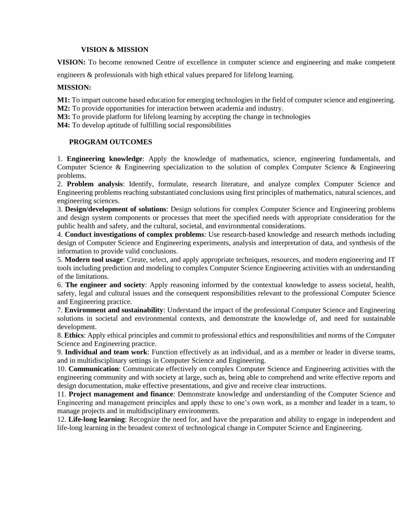
VISION & MISSION VISION: To become renowned Centre of excellence in computer science and engineering and make competent engineers & professionals with high ethical values prepared for lifelong learning. MISSION: M1: To impart outcome based education for emerging technologies in the field of computer science and engineering. M2: To provide opportunities for interaction between academia and industry. M3: To provide platform for lifelong learning by accepting the change in technologies M4: To develop aptitude of fulfilling social responsibilities PROGRAM OUTCOMES 1. Engineering knowledge: Apply the knowledge of mathematics, science, engineering fundamentals, and Computer Science & Engineering specialization to the solution of complex Computer Science & Engineering problems. 2. Problem analysis: Identify, formulate, research literature, and analyze complex Computer Science and Engineering problems reaching substantiated conclusions using first principles of mathematics, natural sciences, and engineering sciences. 3. Design/development of solutions: Design solutions for complex Computer Science and Engineering problems and design system components or processes that meet the specified needs with appropriate consideration for the public health and safety, and the cultural, societal, and environmental considerations. 4. Conduct investigations of complex problems: Use research-based knowledge and research methods including design of Computer Science and Engineering experiments, analysis and interpretation of data, and synthesis of the information to provide valid conclusions. 5. Modern tool usage: Create, select, and apply appropriate techniques, resources, and modern engineering and IT tools including prediction and modeling to complex Computer Science Engineering activities with an understanding of the limitations. 6. The engineer and society: Apply reasoning informed by the contextual knowledge to assess societal, health, safety, legal and cultural issues and the consequent responsibilities relevant to the professional Computer Science and Engineering practice. 7. Environment and sustainability: Understand the impact of the professional Computer Science and Engineering solutions in societal and environmental contexts, and demonstrate the knowledge of, and need for sustainable development. 8. Ethics: Apply ethical principles and commit to professional ethics and responsibilities and norms of the Computer Science and Engineering practice. 9. Individual and team work: Function effectively as an individual, and as a member or leader in diverse teams, and in multidisciplinary settings in Computer Science and Engineering. 10. Communication: Communicate effectively on complex Computer Science and Engineering activities with the engineering community and with society at large, such as, being able to comprehend and write effective reports and design documentation, make effective presentations, and give and receive clear instructions. 11. Project management and finance: Demonstrate knowledge and understanding of the Computer Science and Engineering and management principles and apply these to one’s own work, as a member and leader in a team, to manage projects and in multidisciplinary environments. 12. Life-long learning: Recognize the need for, and have the preparation and ability to engage in independent and life-long learning in the broadest context of technological change in Computer Science and Engineering.
Transcript of VISION & MISSION VISION: MISSION: M1
VISION & MISSION
VISION: To become renowned Centre of excellence in computer science and engineering and make competent
engineers & professionals with high ethical values prepared for lifelong learning.
MISSION:
M1: To impart outcome based education for emerging technologies in the field of computer science and engineering.
M2: To provide opportunities for interaction between academia and industry.
M3: To provide platform for lifelong learning by accepting the change in technologies
M4: To develop aptitude of fulfilling social responsibilities
PROGRAM OUTCOMES
1. Engineering knowledge: Apply the knowledge of mathematics, science, engineering fundamentals, and
Computer Science & Engineering specialization to the solution of complex Computer Science & Engineering
problems.
2. Problem analysis: Identify, formulate, research literature, and analyze complex Computer Science and
Engineering problems reaching substantiated conclusions using first principles of mathematics, natural sciences, and
engineering sciences.
3. Design/development of solutions: Design solutions for complex Computer Science and Engineering problems
and design system components or processes that meet the specified needs with appropriate consideration for the
public health and safety, and the cultural, societal, and environmental considerations.
4. Conduct investigations of complex problems: Use research-based knowledge and research methods including
design of Computer Science and Engineering experiments, analysis and interpretation of data, and synthesis of the
information to provide valid conclusions.
5. Modern tool usage: Create, select, and apply appropriate techniques, resources, and modern engineering and IT
tools including prediction and modeling to complex Computer Science Engineering activities with an understanding
of the limitations.
6. The engineer and society: Apply reasoning informed by the contextual knowledge to assess societal, health,
safety, legal and cultural issues and the consequent responsibilities relevant to the professional Computer Science
and Engineering practice.
7. Environment and sustainability: Understand the impact of the professional Computer Science and Engineering
solutions in societal and environmental contexts, and demonstrate the knowledge of, and need for sustainable
development.
8. Ethics: Apply ethical principles and commit to professional ethics and responsibilities and norms of the Computer
Science and Engineering practice.
9. Individual and team work: Function effectively as an individual, and as a member or leader in diverse teams,
and in multidisciplinary settings in Computer Science and Engineering.
10. Communication: Communicate effectively on complex Computer Science and Engineering activities with the
engineering community and with society at large, such as, being able to comprehend and write effective reports and
design documentation, make effective presentations, and give and receive clear instructions.
11. Project management and finance: Demonstrate knowledge and understanding of the Computer Science and
Engineering and management principles and apply these to one’s own work, as a member and leader in a team, to
manage projects and in multidisciplinary environments.
12. Life-long learning: Recognize the need for, and have the preparation and ability to engage in independent and
life-long learning in the broadest context of technological change in Computer Science and Engineering.

PEO
PEO1: To provide students with the fundamentals of Engineering Sciences with more emphasis in Computer Science
&
Engineering by way of analysing and exploiting engineering challenges.
PEO2: To train students with good scientific and engineering knowledge so as to comprehend, analyse, design, and
create novel products and solutions for the real life problems in Computer Science and Engineering
PEO3: To inculcate professional and ethical attitude, effective communication skills, teamwork skills,
multidisciplinary approach, entrepreneurial thinking and an ability to relate engineering issues with social issues for
Computer Science & Engineering.
PEO4: To provide students with an academic environment aware of excellence, leadership, written ethical codes
and guidelines, and the self-motivated life-long learning needed for a successful professional career in Computer
Science & Engineering.
PEO5: To prepare students to excel in Industry and Higher education by Educating Students along with High moral
values and Knowledge in Computer Science & Engineering.
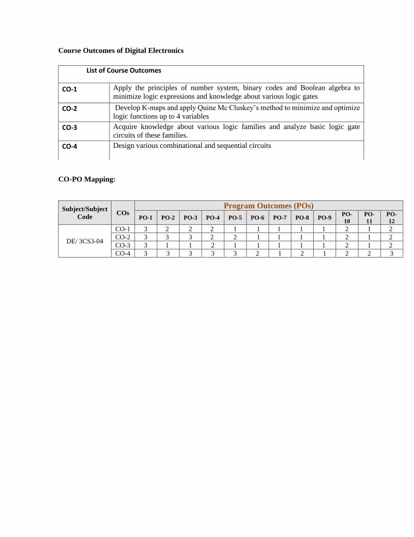
Course Outcomes of Digital Electronics
CO-PO Mapping:
Subject/Subject
Code COs
Program Outcomes (POs)
PO-1 PO-2 PO-3 PO-4 PO-5 PO-6 PO-7 PO-8 PO-9 PO-
10
PO-
11
PO-
12
DE/ 3CS3-04
CO-1 3 2 2 2 1 1 1 1 1 2 1 2
CO-2 3 3 3 2 2 1 1 1 1 2 1 2
CO-3 3 1 1 2 1 1 1 1 1 2 1 2
CO-4 3 3 3 3 3 2 1 2 1 2 2 3
List of Course Outcomes
CO-1 Apply the principles of number system, binary codes and Boolean algebra to
minimize logic expressions and knowledge about various logic gates
CO-2 Develop K-maps and apply Quine Mc Cluskey’s method to minimize and optimize
logic functions up to 4 variables
CO-3 Acquire knowledge about various logic families and analyze basic logic gate
circuits of these families.
CO-4 Design various combinational and sequential circuits

Lecture Plan:
Unit Topics Lect.
Req.
Lect.
No.
Total
Lecture
Required
Unit-
1
1.1. Number systems: binary, Octal, hexadecimal,
Decimal and their interconversions,conversion
binary, Octal, hexadecimal, Decimal and vice versa
1 1
9
1.2. Binary addition, subtraction, multiplication and
division,Octal addition and subtraction; Hexadecimal
addition and subtraction
1 2
1.3. (r-i)'s complements: 1's, 7's, 9's and 15's;r's
complements: 2's, 8's,10's and 16's
1 3 1.4. Subtraction using 1's and 2's
complements,Subtraction using 9's and 10's
complements
1.5. Gray code: Binary to gray conversion and vice-
versaBCD code; Excess-3 code 1 4
1.6. Logic Gates: Basic gates, Universal gates,
Exclusive gates 1 5
1.7. BCD addition; Floating point representation;
Sign and magnitude representation; 2421 code 1 6
1.8. Boolean Algebra: Boolean laws and theorems,
De Morgan's theorem; Duality principle; Minimaize
Boolean expressions using Boolean algebra;
1 7
1.9. Digital Logic: Implementation of Boolean
Expression using Logic gates; Designing diffrerent
logic gates using NAND gates only;
Implementation of Boolean Expression using NAND
gates only 1 8
1.10. Implementation of Logic gates and Boolean
Expressions using NOR gates only, Mixed Logic
gate and Boolean algebra
Unit Test 1 1 9
Unit-
2
2.1. Minterm, Maxterm, Sum of product (SOP),
Product of Sum (POS), Canonical (Standard) Sum of
Product Form, Conversion of any Boolean Function
into Canonical SOP form, Canonical (Standard)
Form of Product of Sum (POS),
1 10
7
2.2. Conversion of a Boolean Function into
Canonical Product of Sum Form, Conversion of
Truth Table in POS and SOP form and vice-versa
1 11
2.3. K–Map: Looping, Simplification of Logic
Function with K-Map 1 12
2.4. K Map Numericals, 2,3, 4 variable K-Map 1 13
2.5. Don’t Care Combinations or Incompletely
Specified Function in K-Map,Variable – Entered K–
maps
1 14
2.6. Quine–MC' cluskey (Tabular) Method 1 15
Unit Test 2 1 16
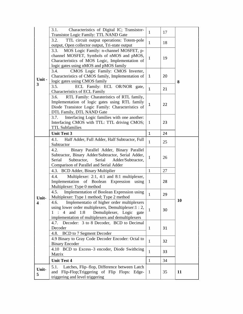
Unit -
3
3.1. Characteristics of Digital IC; Transistor-
Transistor Logic Family: TTL NAND Gate 1 17
8
3.2. TTL circuit output operations: Totem-pole
output, Open collector output, Tri-state output 1 18
3.3. MOS Logic Family: n-channel MOSFET, p-
channel MOSFET, Symbols of nMOS and pMOS,
Characteristics of MOS Logic, Implementation of
logic gates using nMOS and pMOS family
1 19
3.4. CMOS Logic Family: CMOS Inverter,
Characteristics of CMOS family, Implementation of
logic gates using CMOS family
1 20
3.5. ECL Family: ECL OR/NOR gate,
Characteristics of ECL Family 1 21
3.6. RTL Family: Charateristics of RTL family,
Implementation of logic gates using RTL family
Diode Transistor Logic Family: Characteristics of
DTL Family, DTL NAND Gate
1 22
3.7. Interfacing Logic families with one another:
Interfacing CMOS with TTL: TTL driving CMOS;
TTL Subfamilies
1 23
Unit Test 3 1 24
Unit-
4
4.1. Half Adder, Full Adder, Half Subtractor, Full
Subtractor 1 25
10
4.2. Binary Parallel Adder, Binary Parallel
Subtractor, Binary Adder/Subtractor, Serial Adder,
Serial Subtractor, Serial Adder/Subtractor,
Comparison of Parallel and Serial Adder
1 26
4.3. BCD Adder, Binary Multiplier 1 27
4.4. Multiplexer: 2:1, 4:1 and 8:1 multiplexer,
Implementation of Boolean Expression using
Multiplexer: Type 0 method
1 28
4.5. Implementation of Boolean Expression using
Multiplexer: Type 1 method; Type 2 method 1 29
4.6. Implementatio of higher order multiplexers
using lower order multiplexers, Demultiplexer:1 : 2,
1 : 4 and 1:8 Demuliplexer, Logic gate
implementation of multiplexers and demultiplexers
1 30
4.7. Decoder: 3 to 8 Decoder, BCD to Decimal
Decoder 1 31 4.8. BCD to 7 Segment Decoder
4.9 Binary to Gray Code Decoder Encoder: Octal to
Binary Encoder 1 32
4.10 BCD to Excess–3 encoder, Diode Swithcing
Matrix 1 33
Unit Test 4 1 34
Unit-
5
5.1. Latches, Flip–flop, Difference between Latch
and Flip-Flop;Triggering of Flip Flops: Edge-
triggering and level triggering
1 35 11
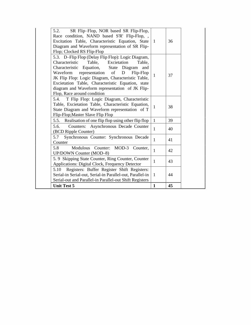
5.2. SR Flip–Flop, NOR based SR Flip-Flop,
Race condition, NAND based S'R' Flip-Flop, ,
Excitation Table, Characteristic Equation, State
Diagram and Waveform representation of SR Flip-
Flop; Clocked RS Flip-Flop
1 36
5.3. D–Flip Flop (Delay Flip Flop): Logic Diagram,
Characteristic Table, Excietation Table,
Characteristic Equation, State Diagram and
Waveform representation of D Flip-Flop
JK Flip Flop: Logic Diagram, Characteristic Table,
Excietation Table, Characteristic Equation, state
diagram and Waveform representation of JK Flip-
Flop, Race around condition
1 37
5.4. T Flip Flop: Logic Diagram, Characteristic
Table, Excietation Table, Characteristic Equation,
State Diagram and Waveform representation of T
Flip-Flop;Master Slave Flip Flop
1 38
5.5. Realisation of one flip flop using other flip flop 1 39
5.6. Counters: Asynchronous Decade Counter
(BCD Ripple Counter) 1 40
5.7 Synchronous Counter: Synchronous Decade
Counter 1 41
5.8 Modulous Counter: MOD-3 Counter,
UP/DOWN Counter (MOD–8) 1 42
5. 9 Skipping State Counter, Ring Counter, Counter
Applications: Digital Clock, Frequency Detector 1 43
5.10 Registers: Buffer Register Shift Registers:
Serial-in Serial-out, Serial-in Parallel-out, Parallel-in
Serial-out and Parallel-in Parallel-out Shift Registers
1 44
Unit Test 5 1 45
Notes:
UNIT-1
Number system,Boolean algebra and Logic gates
Numerical Presentation
The quantities that are to be measured, monitored, recorded, processed and controlled are
analog and digital, depending on the type of system used. It is important when dealing with
various quantities that we be able to represent their values efficiently and accurately. There
are basically two ways of representing the numerical value of quantities: analog and digital.
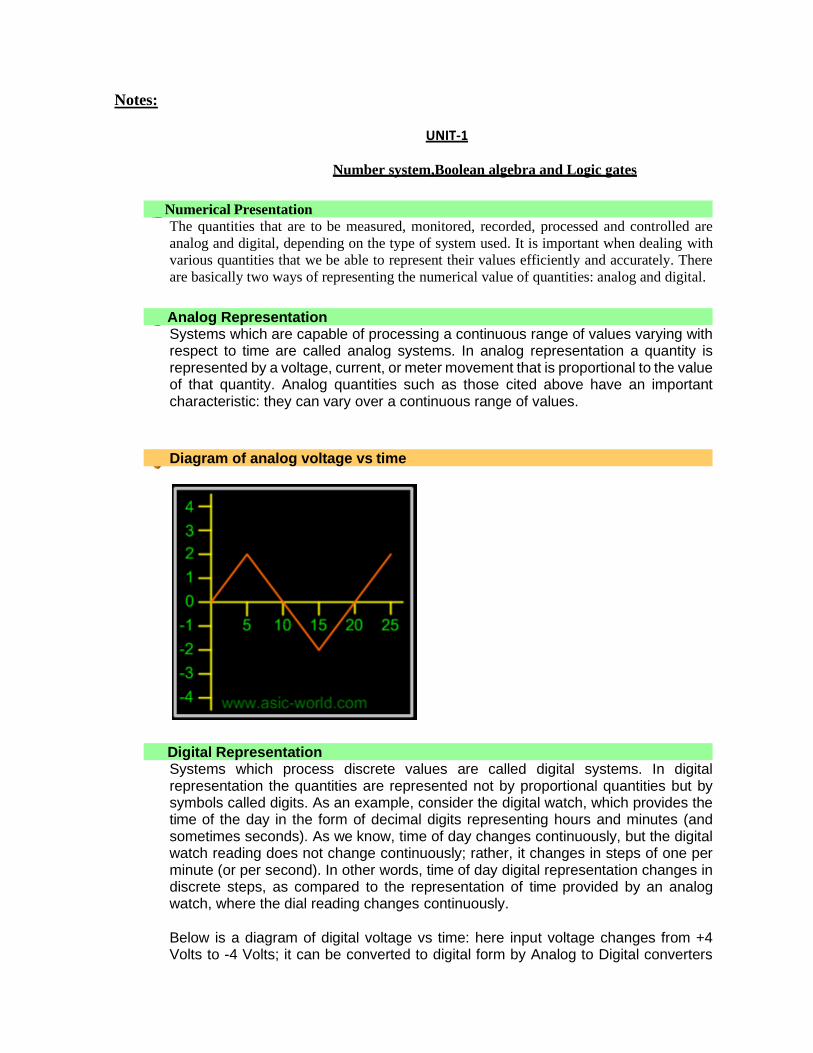
Analog Representation Systems which are capable of processing a continuous range of values varying with respect to time are called analog systems. In analog representation a quantity is represented by a voltage, current, or meter movement that is proportional to the value of that quantity. Analog quantities such as those cited above have an important characteristic: they can vary over a continuous range of values.
Diagram of analog voltage vs time
Digital Representation Systems which process discrete values are called digital systems. In digital representation the quantities are represented not by proportional quantities but by symbols called digits. As an example, consider the digital watch, which provides the time of the day in the form of decimal digits representing hours and minutes (and sometimes seconds). As we know, time of day changes continuously, but the digital watch reading does not change continuously; rather, it changes in steps of one per minute (or per second). In other words, time of day digital representation changes in discrete steps, as compared to the representation of time provided by an analog watch, where the dial reading changes continuously.
Below is a diagram of digital voltage vs time: here input voltage changes from +4 Volts to -4 Volts; it can be converted to digital form by Analog to Digital converters
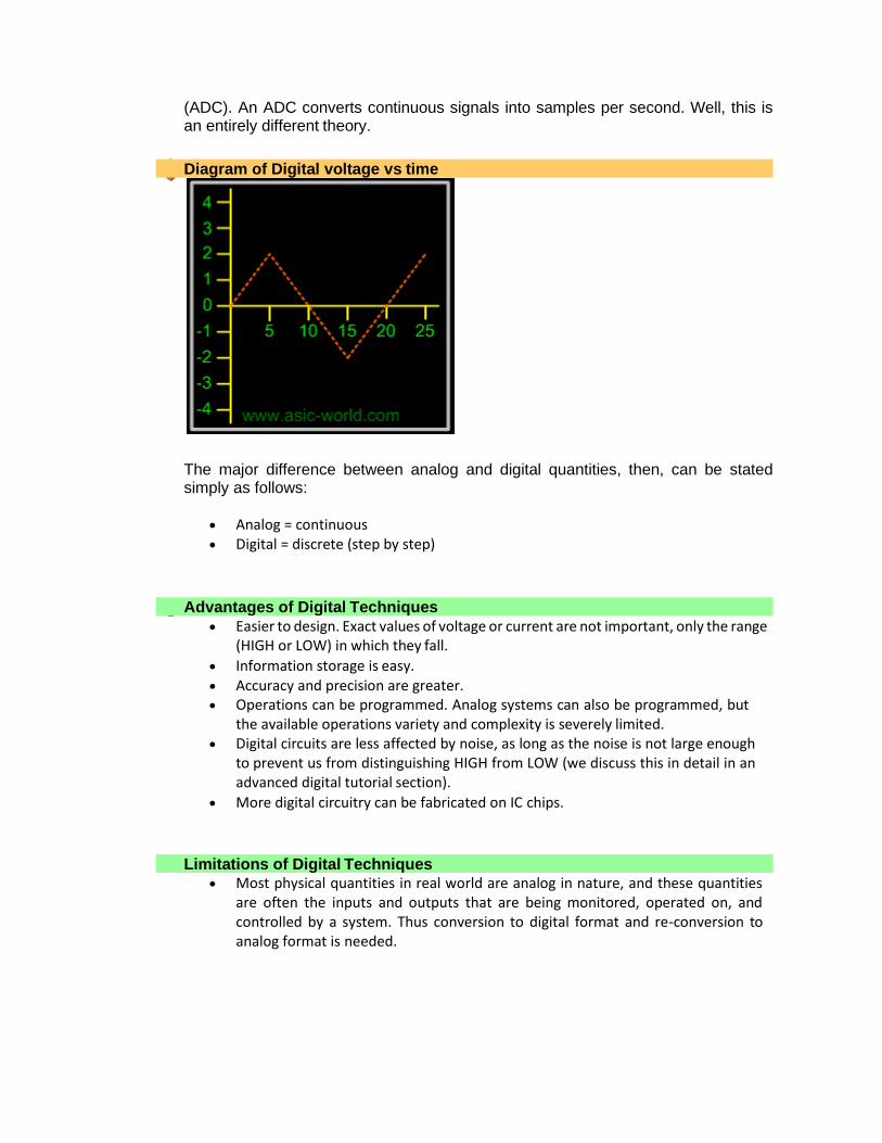
(ADC). An ADC converts continuous signals into samples per second. Well, this is an entirely different theory.
Diagram of Digital voltage vs time
The major difference between analog and digital quantities, then, can be stated simply as follows:
• Analog = continuous • Digital = discrete (step by step)
Advantages of Digital Techniques
• Easier to design. Exact values of voltage or current are not important, only the range (HIGH or LOW) in which they fall.
• Information storage is easy. • Accuracy and precision are greater. • Operations can be programmed. Analog systems can also be programmed, but
the available operations variety and complexity is severely limited. • Digital circuits are less affected by noise, as long as the noise is not large enough
to prevent us from distinguishing HIGH from LOW (we discuss this in detail in an advanced digital tutorial section).
• More digital circuitry can be fabricated on IC chips.
Limitations of Digital Techniques • Most physical quantities in real world are analog in nature, and these quantities
are often the inputs and outputs that are being monitored, operated on, and controlled by a system. Thus conversion to digital format and re-conversion to analog format is needed.
Numbering System
Many number systems are in use in digital technology. The most common are the decimal, binary, octal, and hexadecimal systems. The decimal system is clearly the most familiar to us because it is a tool that we use every day. Examining some of its characteristics will help us to better understand the other systems. In the next few pages we shall introduce four numerical representation systems that are used in the digital system. There are other systems, which we will look at briefly.
• Decimal
• Binary • Octal • Hexadecimal
Decimal System
The decimal system is composed of 10 numerals or symbols. These 10 symbols are 0, 1,
2, 3, 4, 5, 6, 7, 8, 9. Using these symbols as digits of a
number, we can express any quantity. The decimal system is also called
the base-10 system because it has 10 digits.
103 102 101 100 10-1 10-2 10-3
=1000 =100 =10 =1 . =0.1 =0.01 =0.001
Most Significant Digit
Decimal point
Least Significant Digit
Even though the decimal system has only 10 symbols, any number of any magnitude can be expressed by using our system of positional weighting.
Decimal Examples
• 3.1410
• 5210 • 102410 • 6400010
Binary System
In the binary system, there are only two symbols or possible digit values, 0 and 1.
This base-2 system can be used to represent any quantity that can
be represented in decimal or other base system.
23 22 21 20 2-1 2-2 2-3
=8 =4 =2 =1 . =0.5 =0.25 =0.125
Most Significant Binary point Least
Digit Significant Digit
Binary Counting
The Binary counting sequence is shown in the table:
23 22 21 20 Decimal
0 0 0 0 0
0 0 0 1 1
0 0 1 0 2
0 0 1 1 3
0 1 0 0 4
0 1 0 1 5
0 1 1 0 6
0 1 1 1 7
1 0 0 0 8
1 0 0 1 9
1 0 1 0 10
1 0 1 1 11
1 1 0 0 12
1 1 0 1 13
1 1 1 0 14
1 1 1 1 15
Representing Binary Quantities
In digital systems the information that is being processed is usually presented in binary form. Binary quantities can be represented by any device that has only two operating states or possible conditions. E.g.. a switch is only open or closed. We arbitrarily (as we define them) let an open switch represent binary 0 and a closed switch represent binary 1. Thus we can represent any binary number by using series of switches.
Typical Voltage Assignment
Binary 1: Any voltage between 2V to 5V
Binary 0: Any voltage between 0V to 0.8V
Not used: Voltage between 0.8V to 2V in 5 Volt CMOS and TTL Logic, this may cause error in a digital circuit. Today's digital circuits works at 1.8 volts, so this statement may not hold true for all logic circuits.
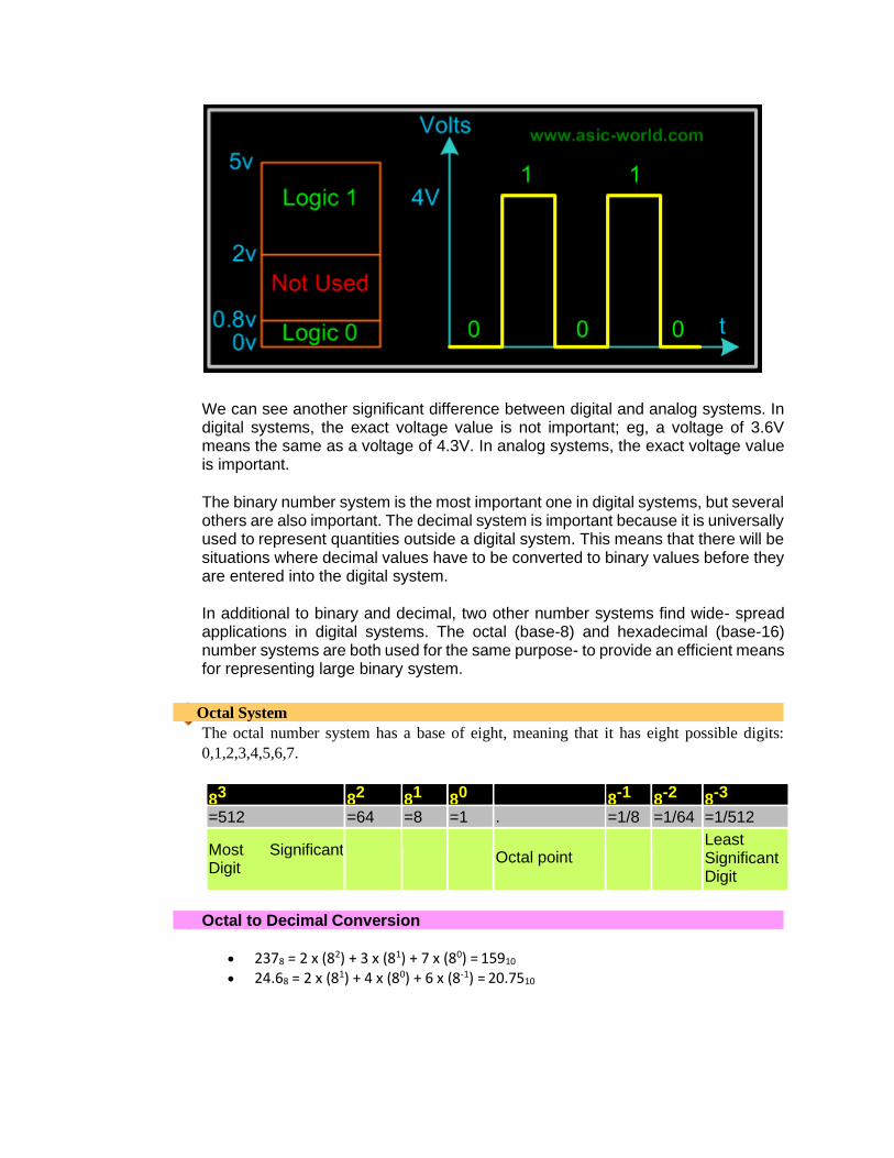
We can see another significant difference between digital and analog systems. In digital systems, the exact voltage value is not important; eg, a voltage of 3.6V means the same as a voltage of 4.3V. In analog systems, the exact voltage value is important.
The binary number system is the most important one in digital systems, but several others are also important. The decimal system is important because it is universally used to represent quantities outside a digital system. This means that there will be situations where decimal values have to be converted to binary values before they are entered into the digital system.
In additional to binary and decimal, two other number systems find wide- spread applications in digital systems. The octal (base-8) and hexadecimal (base-16) number systems are both used for the same purpose- to provide an efficient means for representing large binary system.
Octal System
The octal number system has a base of eight, meaning that it has eight possible digits:
0,1,2,3,4,5,6,7.
83 82 81 80 8-1 8-2 8-3
=512 =64 =8 =1 . =1/8 =1/64 =1/512
Most Significant Digit
Octal point
Least Significant Digit
Octal to Decimal Conversion
• 2378 = 2 x (82) + 3 x (81) + 7 x (80) = 15910 • 24.68 = 2 x (81) + 4 x (80) + 6 x (8-1) = 20.7510

• 11.18 = 1 x (81) + 1 x (80) + 1 x (8-1) = 9.12510 • 12.38 = 1 x (81) + 2 x (80) + 3 x (8-1) = 10.37510
Hexadecimal System
The hexadecimal system uses base 16. Thus, it has 16 possible digit symbols. It uses the
digits 0 through 9 plus the letters A, B, C, D, E, and F
as the 16 digit symbols.
163 162 161 160 16-1 16-2 16-3
=4096 =256 =16 =1 . =1/16 =1/256 =1/4096
Most Significant Digit
Hexa Decimal point
Least Significant Digit
Hexadecimal to Decimal Conversion
• 24.616 = 2 x (161) + 4 x (160) + 6 x (16-1) = 36.37510 • 11.116 = 1 x (161) + 1 x (160) + 1 x (16-1) = 17.062510 • 12.316 = 1 x (161) + 2 x (160) + 3 x (16-1) = 18.187510
Code Conversion Converting from one code form to another code form is called code
conversion, like converting from binary to decimal or converting from hexadecimal to decimal.
Binary-To-Decimal Conversion
Any binary number can be converted to its decimal equivalent simply
by summing together the weights of the various positions in the
binary number which contain a 1.
Binary Decimal
110112
24+23+01+21+20 =16+8+0+2+1
Result 2710
and
Binary Decimal
101101012
27+06+25+24+03+22+01+20 =128+0+32+16+0+4+0+1
Result 18110
You should have noticed that the method is to find the weights (i.e., powers of 2) for each bit position that contains a 1, and then to add them up.
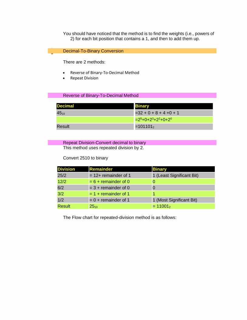
Decimal-To-Binary Conversion
There are 2 methods:
• Reverse of Binary-To-Decimal Method • Repeat Division
Reverse of Binary-To-Decimal Method
Decimal Binary
4510 =32 + 0 + 8 + 4 +0 + 1
=25+0+23+22+0+20
Result =1011012
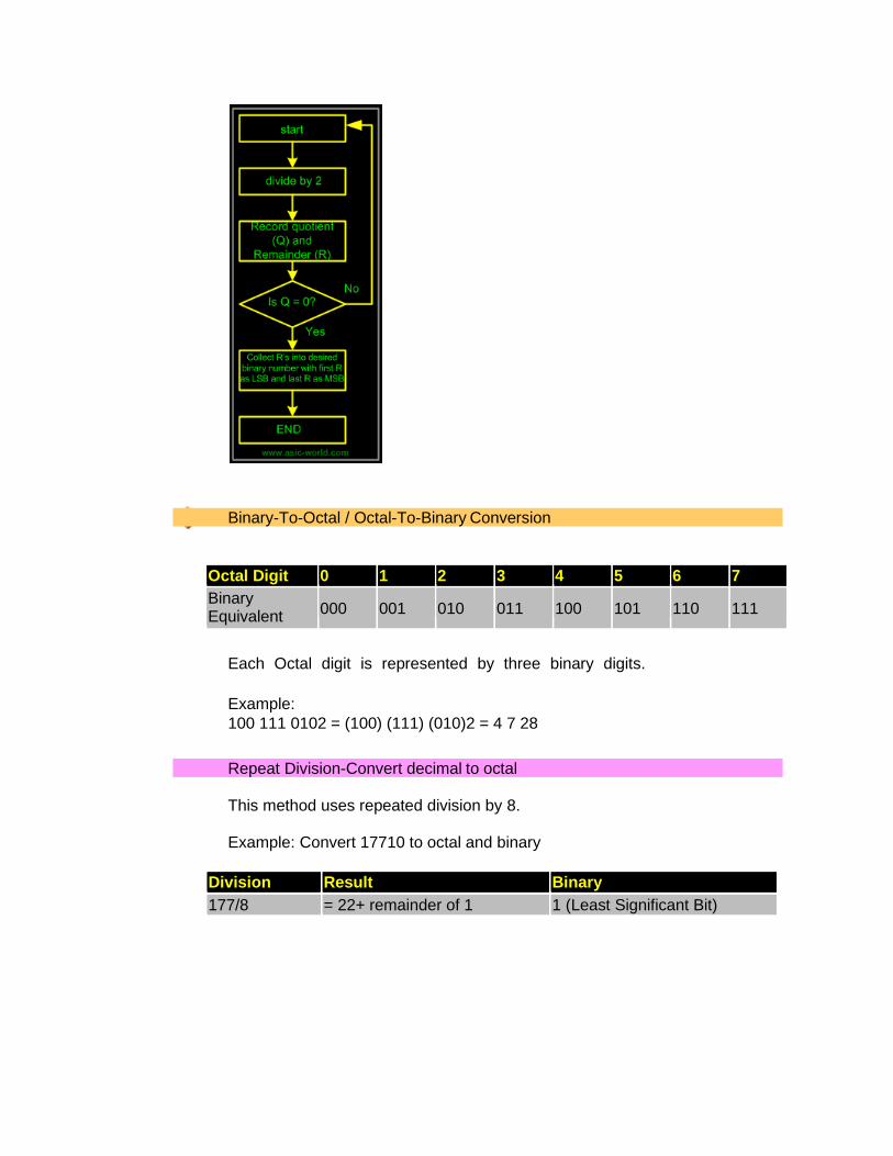
Repeat Division-Convert decimal to binary This method uses repeated division by 2.
Convert 2510 to binary
Division Remainder Binary
25/2 = 12+ remainder of 1 1 (Least Significant Bit)
12/2 = 6 + remainder of 0 0
6/2 = 3 + remainder of 0 0
3/2 = 1 + remainder of 1 1
1/2 = 0 + remainder of 1 1 (Most Significant Bit)
Result 2510 = 110012
The Flow chart for repeated-division method is as follows:
Binary-To-Octal / Octal-To-Binary Conversion
Octal Digit 0 1 2 3 4 5 6 7
Binary Equivalent
000 001 010 011 100 101 110 111
Each Octal digit is represented by three binary digits.
Example:
100 111 0102 = (100) (111) (010)2 = 4 7 28
Repeat Division-Convert decimal to octal
This method uses repeated division by 8.
Example: Convert 17710 to octal and binary
Division Result Binary
177/8 = 22+ remainder of 1 1 (Least Significant Bit)
22/ 8 = 2 + remainder of 6 6
2 / 8 = 0 + remainder of 2 2 (Most Significant Bit)
Result 17710 = 2618
Binary = 0101100012
Hexadecimal to Decimal/Decimal to Hexadecimal Conversion
Example: 2AF16 = 2 x (162) + 10 x (161) + 15 x (160) = 68710
Repeat Division- Convert decimal to hexadecimal This method uses repeated division by 16.
Example: convert 37810 to hexadecimal and binary:
Division Result Hexadecimal
378/16 = 23+ remainder of 10 A (Least Significant Bit)23
23/16 = 1 + remainder of 7 7
1/16 = 0 + remainder of 1 1 (Most Significant Bit)
Result 37810 = 17A16
Binary = 0001 0111 10102
Binary-To-Hexadecimal /Hexadecimal-To-Binary Conversion
Hexadecimal Digit 0 1 2 3 4 5 6 7
Binary Equivalent 0000 0001 0010 0011 0100 0101 0110 0111
Hexadecimal Digit 8 9 A B C D E F
Binary Equivalent 1000 1001 1010 1011 1100 1101 1110 1111
Each Hexadecimal digit is represented by four bits of binary digit.
Example:
1011 0010 11112 = (1011) (0010) (1111)2 = B 2 F16
Octal-To-Hexadecimal Hexadecimal-To-Octal Conversion
• Convert Octal (Hexadecimal) to Binary first. • Regroup the binary number by three bits per group starting from LSB if Octal
is required. • Regroup the binary number by four bits per group starting from LSB
if Hexadecimal is required.
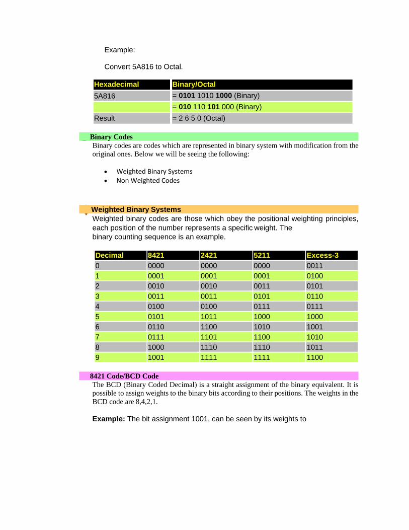
Example:
Convert 5A816 to Octal.
Hexadecimal Binary/Octal
5A816 = 0101 1010 1000 (Binary)
= 010 110 101 000 (Binary)
Result = 2 6 5 0 (Octal)
Binary Codes
Binary codes are codes which are represented in binary system with modification from the
original ones. Below we will be seeing the following:
• Weighted Binary Systems • Non Weighted Codes
Weighted Binary Systems
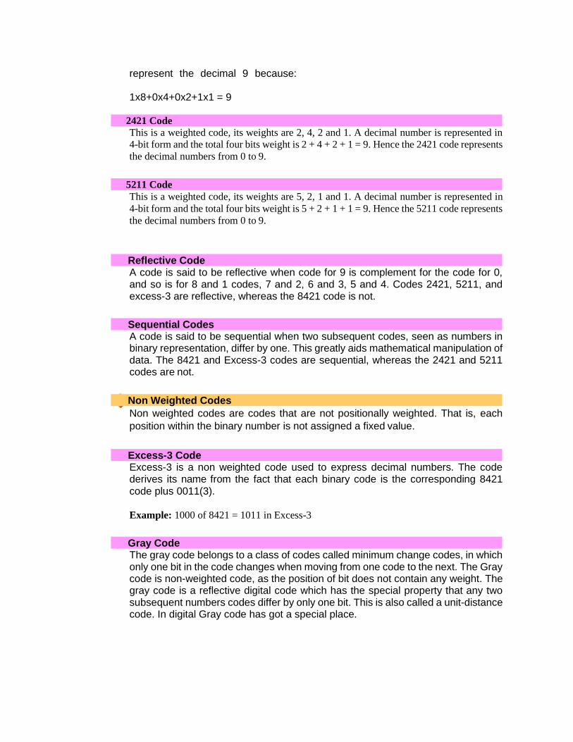
Weighted binary codes are those which obey the positional weighting principles,
each position of the number represents a specific weight. The
binary counting sequence is an example.
Decimal 8421 2421 5211 Excess-3
0 0000 0000 0000 0011
1 0001 0001 0001 0100
2 0010 0010 0011 0101
3 0011 0011 0101 0110
4 0100 0100 0111 0111
5 0101 1011 1000 1000
6 0110 1100 1010 1001
7 0111 1101 1100 1010
8 1000 1110 1110 1011
9 1001 1111 1111 1100
8421 Code/BCD Code
The BCD (Binary Coded Decimal) is a straight assignment of the binary equivalent. It is
possible to assign weights to the binary bits according to their positions. The weights in the
BCD code are 8,4,2,1.
Example: The bit assignment 1001, can be seen by its weights to
represent the decimal 9 because:
1x8+0x4+0x2+1x1 = 9
2421 Code
This is a weighted code, its weights are 2, 4, 2 and 1. A decimal number is represented in
4-bit form and the total four bits weight is 2 + 4 + 2 + 1 = 9. Hence the 2421 code represents
the decimal numbers from 0 to 9.
5211 Code
This is a weighted code, its weights are 5, 2, 1 and 1. A decimal number is represented in
4-bit form and the total four bits weight is 5 + 2 + 1 + 1 = 9. Hence the 5211 code represents
the decimal numbers from 0 to 9.
Reflective Code A code is said to be reflective when code for 9 is complement for the code for 0, and so is for 8 and 1 codes, 7 and 2, 6 and 3, 5 and 4. Codes 2421, 5211, and excess-3 are reflective, whereas the 8421 code is not.
Sequential Codes A code is said to be sequential when two subsequent codes, seen as numbers in binary representation, differ by one. This greatly aids mathematical manipulation of data. The 8421 and Excess-3 codes are sequential, whereas the 2421 and 5211 codes are not.
Non Weighted Codes
Non weighted codes are codes that are not positionally weighted. That is, each
position within the binary number is not assigned a fixed value.
Excess-3 Code Excess-3 is a non weighted code used to express decimal numbers. The code derives its name from the fact that each binary code is the corresponding 8421 code plus 0011(3).
Example: 1000 of 8421 = 1011 in Excess-3
Gray Code The gray code belongs to a class of codes called minimum change codes, in which only one bit in the code changes when moving from one code to the next. The Gray code is non-weighted code, as the position of bit does not contain any weight. The gray code is a reflective digital code which has the special property that any two subsequent numbers codes differ by only one bit. This is also called a unit-distance code. In digital Gray code has got a special place.
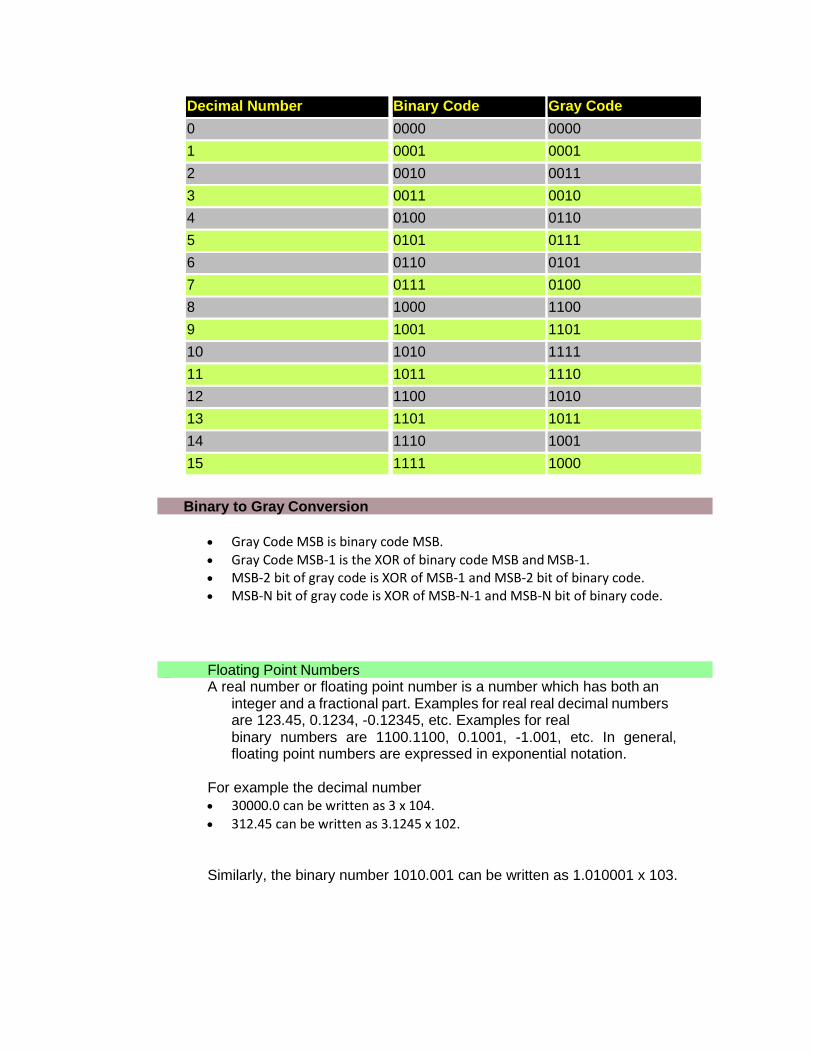
Decimal Number Binary Code Gray Code
0 0000 0000
1 0001 0001
2 0010 0011
3 0011 0010
4 0100 0110
5 0101 0111
6 0110 0101
7 0111 0100
8 1000 1100
9 1001 1101
10 1010 1111
11 1011 1110
12 1100 1010
13 1101 1011
14 1110 1001
15 1111 1000
Binary to Gray Conversion
• Gray Code MSB is binary code MSB. • Gray Code MSB-1 is the XOR of binary code MSB and MSB-1. • MSB-2 bit of gray code is XOR of MSB-1 and MSB-2 bit of binary code. • MSB-N bit of gray code is XOR of MSB-N-1 and MSB-N bit of binary code.
Floating Point Numbers A real number or floating point number is a number which has both an
integer and a fractional part. Examples for real real decimal numbers are 123.45, 0.1234, -0.12345, etc. Examples for real binary numbers are 1100.1100, 0.1001, -1.001, etc. In general, floating point numbers are expressed in exponential notation.
For example the decimal number
• 30000.0 can be written as 3 x 10⁴.
• 312.45 can be written as 3.1245 x 10².
Similarly, the binary number 1010.001 can be written as 1.010001 x 10³.
The general form of a number N can be expressed as N =
± m x b±e.
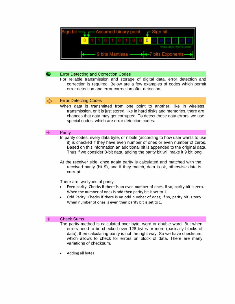
Where m is mantissa, b is the base of number system and e is the exponent. A floating point number is represented by two parts. The number first part, called mantissa, is a signed fixed point number and the second part, called exponent, specifies the decimal or binary position.
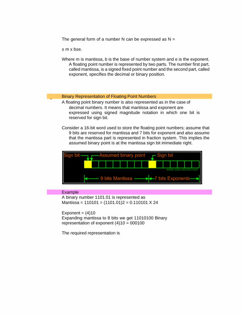
Binary Representation of Floating Point Numbers
A floating point binary number is also represented as in the case of
decimal numbers. It means that mantissa and exponent are expressed using signed magnitude notation in which one bit is reserved for sign bit.
Consider a 16-bit word used to store the floating point numbers; assume that
9 bits are reserved for mantissa and 7 bits for exponent and also assume that the mantissa part is represented in fraction system. This implies the assumed binary point is at the mantissa sign bit immediate right.
Example
A binary number 1101.01 is represented as
Mantissa = 110101 = (1101.01)2 = 0.110101 X 24
Exponent = (4)10 Expanding mantissa to 8 bits we get 11010100 Binary representation of exponent (4)10 = 000100
The required representation is
Error Detecting and Correction Codes
For reliable transmission and storage of digital data, error detection and correction is required. Below are a few examples of codes which permit error detection and error correction after detection.
Error Detecting Codes
When data is transmitted from one point to another, like in wireless transmission, or it is just stored, like in hard disks and memories, there are chances that data may get corrupted. To detect these data errors, we use special codes, which are error detection codes.
Parity
In parity codes, every data byte, or nibble (according to how user wants to use it) is checked if they have even number of ones or even number of zeros. Based on this information an additional bit is appended to the original data. Thus if we consider 8-bit data, adding the parity bit will make it 9 bit long.
At the receiver side, once again parity is calculated and matched with the
received parity (bit 9), and if they match, data is ok, otherwise data is corrupt.
There are two types of parity: • Even parity: Checks if there is an even number of ones; if so, parity bit is zero.
When the number of ones is odd then parity bit is set to 1. • Odd Parity: Checks if there is an odd number of ones; if so, parity bit is zero.
When number of ones is even then parity bit is set to 1.
Check Sums The parity method is calculated over byte, word or double word. But when
errors need to be checked over 128 bytes or more (basically blocks of data), then calculating parity is not the right way. So we have checksum, which allows to check for errors on block of data. There are many variations of checksum.
• Adding all bytes
• CRC • Fletcher's checksum • Adler-32
The simplest form of checksum, which simply adds up the asserted bits in the data, cannot detect a number of types of errors. In particular, such a checksum is not changed by:
• Reordering of the bytes in the message
• Inserting or deleting zero-valued bytes • Multiple errors which sum to zero
Example of Checksum : Given 4 bytes of data (can be done with any number
of bytes): 25h, 62h, 3Fh, 52h
• Adding all bytes together gives 118h.
• Drop the Carry Nibble to give you 18h. • Get the two's complement of the 18h to get E8h. This is the checksum
byte.
To Test the Checksum byte simply add it to the original group of bytes.
This should give you 200h.
Drop the carry nibble again giving 00h. Since it is 00h this means the checksum means the bytes were probably not changed.
Error-Correcting Codes
Error-correcting codes not only detect errors, but also correct them.
This is used normally in Satellite communication, where turn-around delay is very high as is the probability of data getting corrupt.
ECC (Error correcting codes) are used also in memories, networking, Hard
disk, CDROM, DVD etc. Normally in networking chips (ASIC), we have 2 Error detection bits and 1 Error correction bit.
Hamming Code Hamming code adds a minimum number of bits to the data transmitted
in a noisy channel, to be able to correct every possible one-bit error. It can detect (not correct) two-bits errors and cannot distinguish between 1-bit and 2-bits inconsistencies. It can't - in general - detect 3(or more)-bits errors.
The idea is that the failed bit position in an n-bit string (which we'll call
X) can be represented in binary with log2(n) bits, hence we'll try to get it adding just log2(n) bits.
First, we set m = n + log2(n) to the encoded string length and we number
each bit position starting from 1 through m. Then we place these additional bits at power-of-two positions, that is 1, 2, 4, 8..., while remaining ones (3, 5, 6, 7...) hold the bit string in the original order.
Now we set each added bit to the parity of a group of bits. We group bits
this way: we form a group for every parity bit, where the following relation holds:
position(bit) AND position(parity) = position(parity) (Note that: AND is the bit-wise boolean AND; parity bits are included in the
groups; each bit can belong to one or more groups.)
So bit 1 groups bits 1, 3, 5, 7... while bit 2 groups bits 2, 3, 6, 7, 10... , bit 4 groups bits 4, 5, 6, 7, 12, 13... and so on.
Thus, by definition, X (the failed bit position defined above) is the sum of the
incorrect parity bits positions (0 for no errors).
To understand why it is so, let's call Xn the nth bit of X in binary representation. Now consider that each parity bit is tied to a bit of X: parity1 -> X1, parity2 -> X2, parity4 -> X3, parity8 -> X4 and so on - for programmers: they are the respective AND masks -. By construction, the failed bit makes fail only the parity bits which correspond to the 1s in X, so each bit of X is 1 if the corresponding parity is wrong and 0 if it is correct.
Note that the longer the string, the higher the throughput n/m and the lower
the probability that no more than one bit fails. So the string to be sent should be broken into blocks whose length depends on the transmission channel quality (the cleaner the channel, the bigger the block). Also, unless it's guaranteed that at most one bit per block fails, a checksum or some other form of data integrity check should be added.
Alphanumeric Codes
The binary codes that can be used to represent all the letters of the
alphabet, numbers and mathematical symbols, punctuation marks, are known as alphanumeric codes or character codes. These codes enable us to interface the input-output devices like the keyboard, printers, video displays with the computer.
ASCII Code ASCII stands for American Standard Code for Information Interchange.
It has become a world standard alphanumeric code for microcomputers and computers. It is a 7-bit code representing 27 = 128 different characters. These characters represent 26 upper case letters (A to Z), 26 lowercase letters (a to z), 10 numbers (0 to 9), 33 special characters and symbols and 33 control characters.
The 7-bit code is divided into two portions, The leftmost 3 bits portion is called
zone bits and the 4-bit portion on the right is called numeric bits.
An 8-bit version of ASCII code is known as USACC-II 8 or ASCII-8. The 8-bit version can represent a maximum of 256 characters.
EBCDIC Code EBCDIC stands for Extended Binary Coded Decimal Interchange. It is
mainly used with large computer systems like mainframes. EBCDIC is an 8-bit code and thus accomodates up to 256 characters. An EBCDIC code is divided into two portions: 4 zone bits (on the left) and 4 numeric bits (on the right).
Symbolic Logic Boolean algebra derives its name from the mathematician George Boole. Symbolic Logic uses values, variables and operations :
• True is represented by the value 1. • False is represented by the value 0.
Variables are represented by letters and can have one of two values, either 0 or 1. Operations are functions of one or more variables.
• AND is represented by X.Y • OR is represented by X + Y • NOT is represented by X' . Throughout this tutorial the X' form
will be used and sometime !X will be used.
These basic operations can be combined to give expressions.
Example :
• X
• X.Y • W.X.Y + Z
Precedence
As with any other branch of mathematics, these operators have an
order of precedence. NOT operations have the
highest precedence, followed by AND operations, followed by
OR operations. Brackets can be used as with other forms of algebra. e.g.
X.Y + Z and X.(Y + Z) are not the same function.
Function Definitions
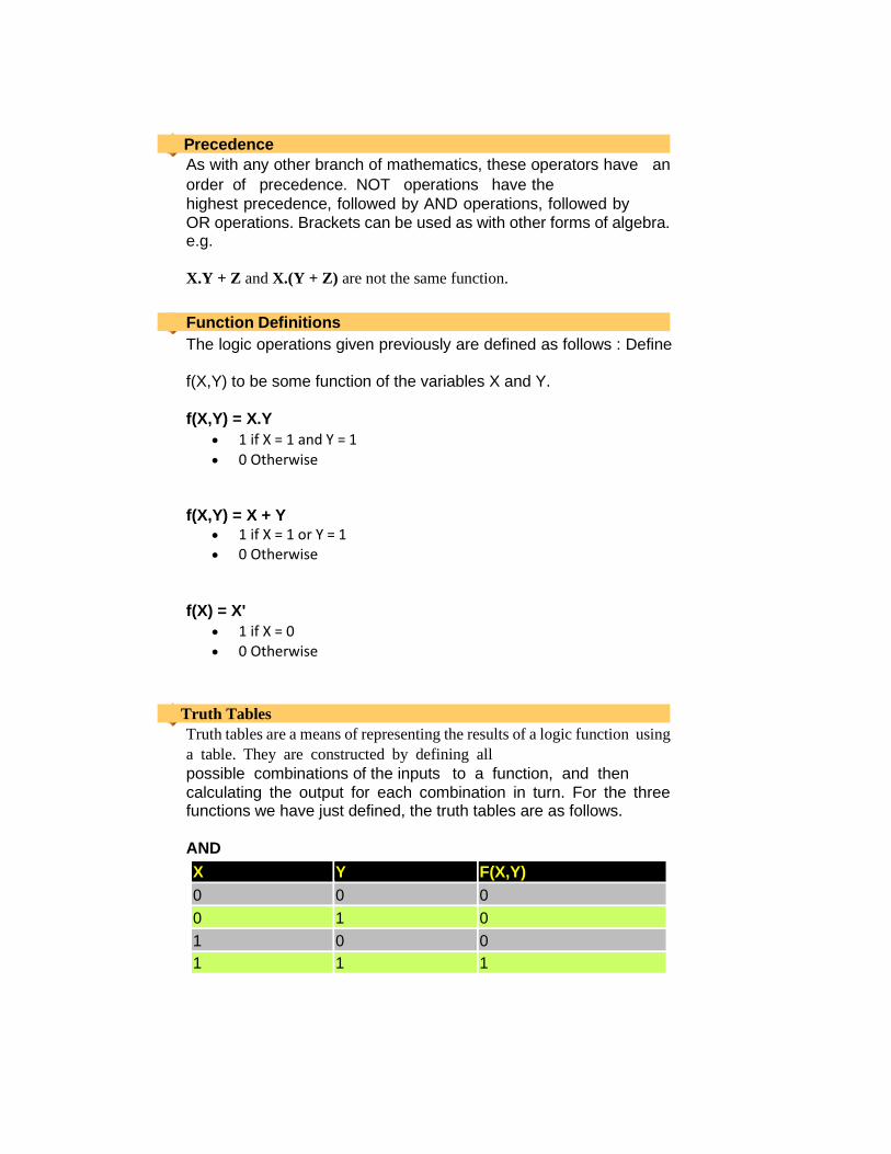
The logic operations given previously are defined as follows : Define
f(X,Y) to be some function of the variables X and Y.
f(X,Y) = X.Y
• 1 if X = 1 and Y = 1
• 0 Otherwise
f(X,Y) = X + Y
• 1 if X = 1 or Y = 1 • 0 Otherwise
f(X) = X'
• 1 if X = 0 • 0 Otherwise
Truth Tables
Truth tables are a means of representing the results of a logic function using
a table. They are constructed by defining all
possible combinations of the inputs to a function, and then
calculating the output for each combination in turn. For the three functions we have just defined, the truth tables are as follows.
AND
X Y F(X,Y)
0 0 0
0 1 0
1 0 0
1 1 1
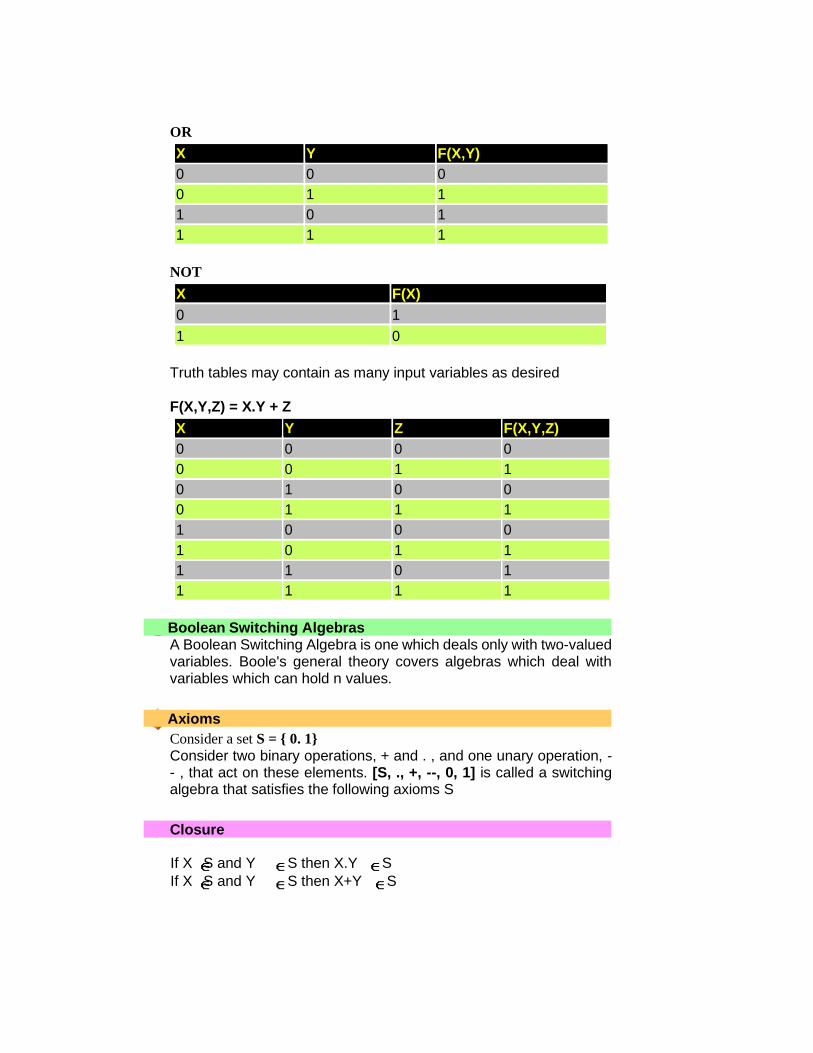
OR
X Y F(X,Y)
0 0 0
0 1 1
1 0 1
1 1 1
NOT
X F(X)
0 1
1 0
Truth tables may contain as many input variables as desired
F(X,Y,Z) = X.Y + Z
X Y Z F(X,Y,Z)
0 0 0 0
0 0 1 1
0 1 0 0
0 1 1 1
1 0 0 0
1 0 1 1
1 1 0 1
1 1 1 1
Boolean Switching Algebras
A Boolean Switching Algebra is one which deals only with two-valued variables. Boole's general theory covers algebras which deal with variables which can hold n values.
Axioms
Consider a set S = { 0. 1}
Consider two binary operations, + and . , and one unary operation, -- , that act on these elements. [S, ., +, --, 0, 1] is called a switching algebra that satisfies the following axioms S
Closure
If X S and Y S then X.Y S
If X S and Y S then X+Y S
an identity 0 for + such that X + 0 = X an identity 1 for . such that X . 1 = X
X + Y = Y + X X . Y = Y . X
X.(Y + Z ) = X.Y + X.Z
X + Y.Z = (X + Y) . (X + Z)
X S a complement X'such that X + X' = 1
X . X' = 0
The complement X' is unique.
Theorems
A number of theorems may be proved for switching algebras
X + X = X X . X = X
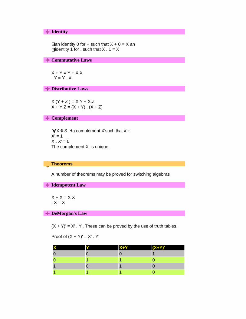
(X + Y)' = X' . Y', These can be proved by the use of truth tables.
Proof of (X + Y)' = X' . Y'
X Y X+Y (X+Y)'
0 0 0 1
0 1 1 0
1 0 1 0
1 1 1 0
Identity
Commutative Laws
Distributive Laws
Complement
Idempotent Law
DeMorgan's Law
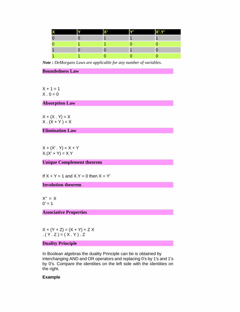
X Y X' Y' X'.Y'
0 0 1 1 1
0 1 1 0 0
1 0 0 1 0
1 1 0 0 0
Note : DeMorgans Laws are applicable for any number of variables.
X + 1 = 1
X . 0 = 0
X + (X . Y) = X X . (X + Y ) = X
X + (X' . Y) = X + Y
X.(X' + Y) = X.Y
If X + Y = 1 and X.Y = 0 then X = Y'
X'' = X 0' = 1
X + (Y + Z) = (X + Y) + Z X . ( Y . Z ) = ( X . Y ) . Z
In Boolean algebras the duality Principle can be is obtained by interchanging AND and OR operators and replacing 0's by 1's and 1's by 0's. Compare the identities on the left side with the identities on the right.
Example
Boundedness Law
Absorption Law
Elimination Law
Unique Complement theorem
Involution theorem
Associative Properties
Duality Principle
X.Y+Z' = (X'+Y').Z
X.Y + X'.Z + Y.Z = X.Y + X'.Z or dual form as below
(X + Y).(X' + Z).(Y + Z) = (X + Y).(X' + Z)
Proof of X.Y + X'.Z + Y.Z = X.Y + X'.Z:
X.Y + X'.Z + Y.Z = X.Y + X'.Z
X.Y + X'.Z + (X+X').Y.Z = X.Y + X'.Z
X.Y.(1+Z) + X'.Z.(1+Y) = X.Y + X'.Z
X.Y + X'.Z = X.Y + X'.Z
(X.Y'+Z).(X+Y).Z = X.Z+Y.Z instead of X.Z+Y'.Z X.Y'Z+X.Z+Y.Z (X.Y'+X+Y).Z (X+Y).Z X.Z+Y.Z
The term which is left out is called the consensus term.
Given a pair of terms for which a variable appears in one term, and its complement in the other, then the consensus term is formed by ANDing the original terms together, leaving out the selected variable and its complement.
Example : The consensus of X.Y and X'.Z is Y.Z
The consensus of X.Y.Z and Y'.Z'.W' is (X.Z).(Z.W')
Summary of Laws And Theorms
Identity Dual
Operations with 0 and 1
X + 0 = X (identity) X.1 = X
X + 1 = 1 (null element) X.0 = 0
Idempotency theorem
X + X = X X.X = X
Complementarity
X + X' = 1 X.X' = 0
Involution theorem
(X')' = X
Cummutative law
X + Y = Y + X X.Y = Y X
Consensus theorem
Associative law
(X + Y) + Z = X + (Y + Z) = X + Y + Z
(XY)Z = X(YZ) = XYZ
Distributive law
X(Y + Z) = XY + XZ X + (YZ) = (X + Y)(X + Z)
DeMorgan's theorem
(X + Y + Z + ...)' = X'Y'Z'... or
{ f ( X1,X2,...,Xn,0,1,+,. ) } = {
f ( X1',X2',...,Xn',1,0,.,+ ) }
(XYZ...)' = X' + Y' + Z' + ...
Simplification theorems
XY + XY' = X (uniting) (X + Y)(X + Y') = X
X + XY = X (absorption) X(X + Y) = X
(X + Y')Y = XY (adsorption) XY' + Y = X + Y
Consensus theorem
XY + X'Z + YZ = XY + X'Z (X + Y)(X' + Z)(Y + Z) = (X + Y)(X' + Z)
Duality
(X + Y + Z + ...)D = XYZ... or
{f(X1,X2,...,Xn,0,1,+,.)}D =
f(X1,X2,...,Xn,1,0,.,+)
(XYZ ...)D = X + Y + Z + ...
Logic Gates A logic gate is an electronic circuit/device which makes the logical decisions. To arrive at this decisions, the most common logic gates used are OR, AND, NOT, NAND, and NOR gates. The NAND and NOR gates are called universal gates. The exclusive-OR gate is another logic gate which can be constructed using AND, OR and NOT gate.
Logic gates have one or more inputs and only one output. The output is active only for certain input combinations. Logic gates are the building blocks of any digital circuit. Logic gates are also called switches. With the advent of integrated circuits, switches have been replaced by TTL (Transistor Transistor Logic) circuits and CMOS circuits. Here I give example circuits on how to construct simples gates.
Symbolic Logic
Boolean algebra derives its name from the mathematician George Boole. Symbolic Logic uses values, variables and operations.
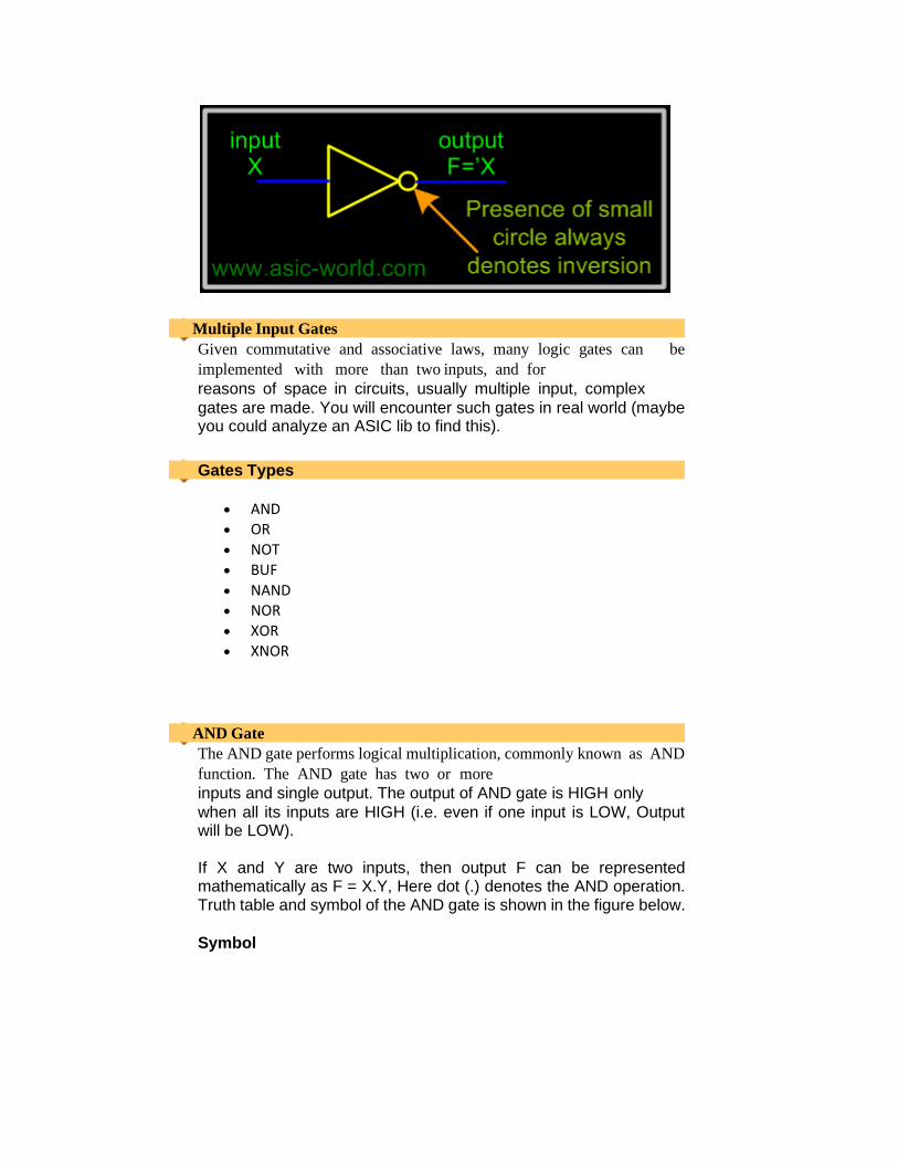
Inversion
A small circle on an input or an output indicates inversion. See the
NOT, NAND and NOR gates given below for examples.
Multiple Input Gates
Given commutative and associative laws, many logic gates can be
implemented with more than two inputs, and for
reasons of space in circuits, usually multiple input, complex
gates are made. You will encounter such gates in real world (maybe you could analyze an ASIC lib to find this).
Gates Types
• AND • OR
• NOT • BUF
• NAND • NOR
• XOR • XNOR
AND Gate
The AND gate performs logical multiplication, commonly known as AND
function. The AND gate has two or more
inputs and single output. The output of AND gate is HIGH only
when all its inputs are HIGH (i.e. even if one input is LOW, Output will be LOW).
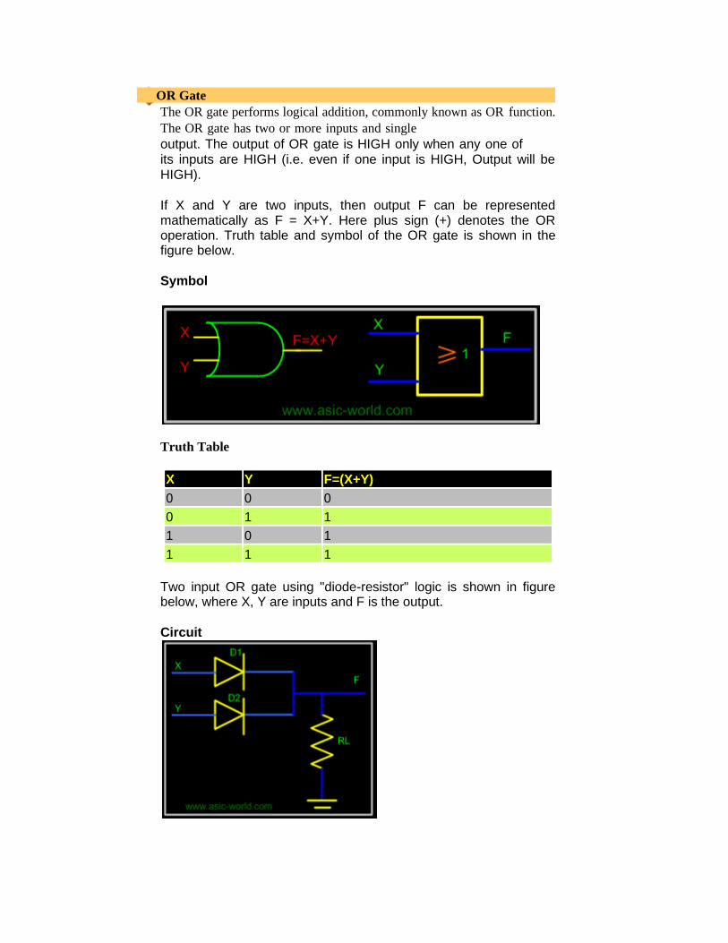
If X and Y are two inputs, then output F can be represented mathematically as F = X.Y, Here dot (.) denotes the AND operation. Truth table and symbol of the AND gate is shown in the figure below.
Symbol
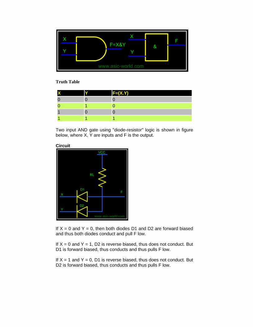
Truth Table
X Y F=(X.Y)
0 0 0
0 1 0
1 0 0
1 1 1
Two input AND gate using "diode-resistor" logic is shown in figure below, where X, Y are inputs and F is the output.
Circuit
If X = 0 and Y = 0, then both diodes D1 and D2 are forward biased and thus both diodes conduct and pull F low.
If X = 0 and Y = 1, D2 is reverse biased, thus does not conduct. But D1 is forward biased, thus conducts and thus pulls F low.
If X = 1 and Y = 0, D1 is reverse biased, thus does not conduct. But D2 is forward biased, thus conducts and thus pulls F low.
If X = 1 and Y = 1, then both diodes D1 and D2 are reverse biased and thus both the diodes are in cut-off and thus there is no drop in voltage at F. Thus F is HIGH.
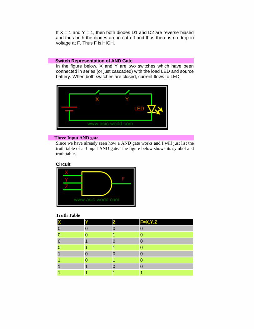
Switch Representation of AND Gate In the figure below, X and Y are two switches which have been connected in series (or just cascaded) with the load LED and source battery. When both switches are closed, current flows to LED.
Three Input AND gate
Since we have already seen how a AND gate works and I will just list the
truth table of a 3 input AND gate. The figure below shows its symbol and
truth table.
Circuit
Truth Table
X Y Z F=X.Y.Z
0 0 0 0
0 0 1 0
0 1 0 0
0 1 1 0
1 0 0 0
1 0 1 0
1 1 0 0
1 1 1 1
OR Gate
The OR gate performs logical addition, commonly known as OR function.
The OR gate has two or more inputs and single
output. The output of OR gate is HIGH only when any one of its inputs are HIGH (i.e. even if one input is HIGH, Output will be HIGH).
If X and Y are two inputs, then output F can be represented mathematically as F = X+Y. Here plus sign (+) denotes the OR operation. Truth table and symbol of the OR gate is shown in the figure below.
Symbol
Truth Table
X Y F=(X+Y)
0 0 0
0 1 1
1 0 1
1 1 1
Two input OR gate using "diode-resistor" logic is shown in figure below, where X, Y are inputs and F is the output.
Circuit
If X = 0 and Y = 0, then both diodes D1 and D2 are reverse biased and thus both the diodes are in cut-off and thus F is low.
If X = 0 and Y = 1, D1 is reverse biased, thus does not conduct. But D2 is forward biased, thus conducts and thus pulling F to HIGH.
If X = 1 and Y = 0, D2 is reverse biased, thus does not conduct. But D1 is forward biased, thus conducts and thus pulling F to HIGH.
If X = 1 and Y = 1, then both diodes D1 and D2 are forward biased and thus both the diodes conduct and thus F is HIGH.
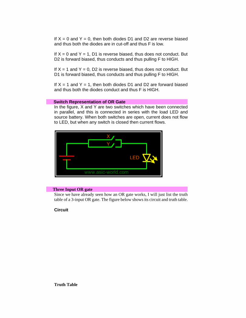
Switch Representation of OR Gate In the figure, X and Y are two switches which have been connected in parallel, and this is connected in series with the load LED and source battery. When both switches are open, current does not flow to LED, but when any switch is closed then current flows.
Three Input OR gate
Since we have already seen how an OR gate works, I will just list the truth
table of a 3-input OR gate. The figure below shows its circuit and truth table.
Circuit
Truth Table
X Y Z F=X+Y+Z
0 0 0 0
0 0 1 1
0 1 0 1
0 1 1 1
1 0 0 1
1 0 1 1
1 1 0 1
1 1 1 1
NOT Gate
The NOT gate performs the basic logical function called inversion or complementation.
NOT gate is also called inverter. The purpose of this
gate is to convert one logic level into the opposite logic level. It has one input and one output. When a HIGH level is applied to an inverter, a LOW level appears on its output and vice versa.
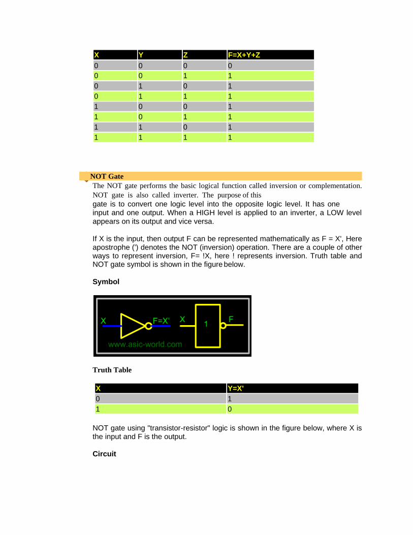
If X is the input, then output F can be represented mathematically as F = X', Here apostrophe (') denotes the NOT (inversion) operation. There are a couple of other ways to represent inversion, F= !X, here ! represents inversion. Truth table and NOT gate symbol is shown in the figure below.
Symbol
Truth Table
X Y=X'
0 1
1 0
NOT gate using "transistor-resistor" logic is shown in the figure below, where X is the input and F is the output.
Circuit
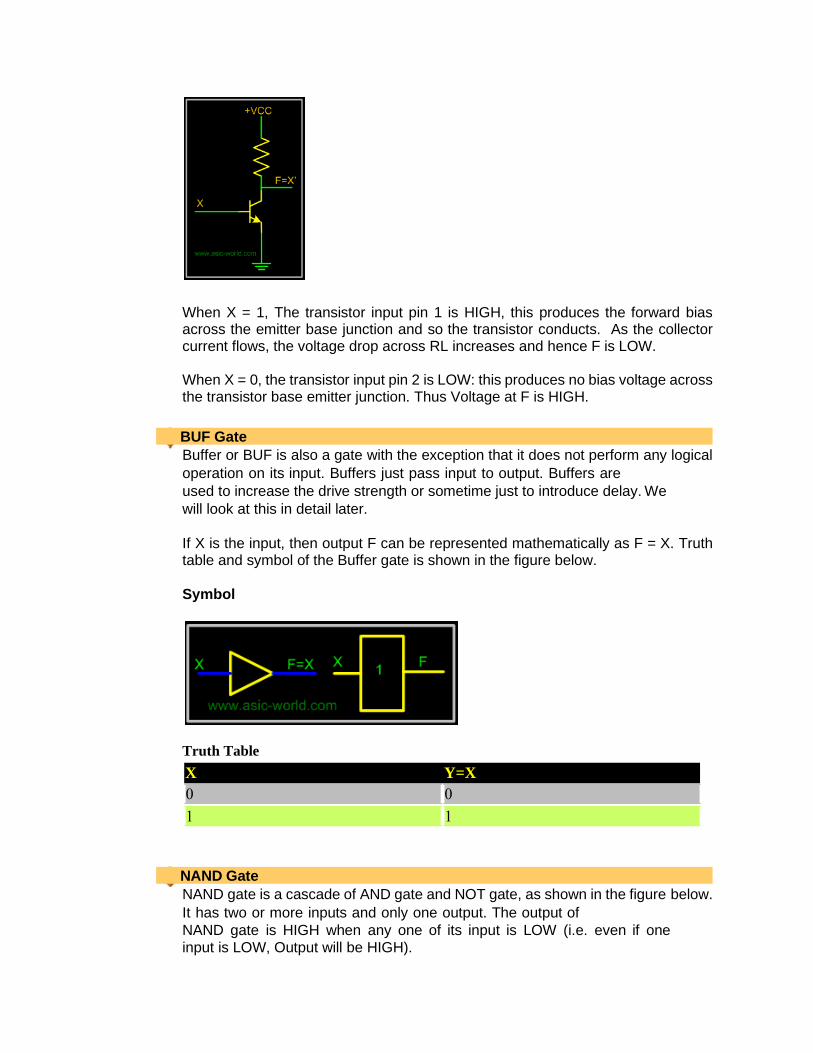
When X = 1, The transistor input pin 1 is HIGH, this produces the forward bias across the emitter base junction and so the transistor conducts. As the collector current flows, the voltage drop across RL increases and hence F is LOW.
When X = 0, the transistor input pin 2 is LOW: this produces no bias voltage across the transistor base emitter junction. Thus Voltage at F is HIGH.
BUF Gate
Buffer or BUF is also a gate with the exception that it does not perform any logical
operation on its input. Buffers just pass input to output. Buffers are
used to increase the drive strength or sometime just to introduce delay. We
will look at this in detail later.
If X is the input, then output F can be represented mathematically as F = X. Truth table and symbol of the Buffer gate is shown in the figure below.
Symbol
Truth Table
NAND Gate
NAND gate is a cascade of AND gate and NOT gate, as shown in the figure below.
It has two or more inputs and only one output. The output of
NAND gate is HIGH when any one of its input is LOW (i.e. even if one
input is LOW, Output will be HIGH).
X Y=X
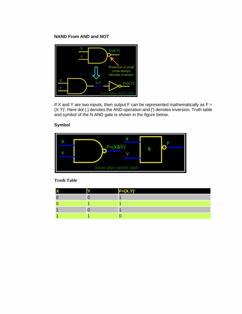
NAND From AND and NOT
If X and Y are two inputs, then output F can be represented mathematically as F = (X.Y)', Here dot (.) denotes the AND operation and (') denotes inversion. Truth table and symbol of the N AND gate is shown in the figure below.
Symbol
Truth Table
X Y F=(X.Y)'
0 0 1
0 1 1
1 0 1
1 1 0
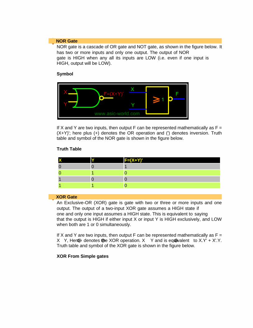
NOR Gate
NOR gate is a cascade of OR gate and NOT gate, as shown in the figure below. It
has two or more inputs and only one output. The output of NOR
gate is HIGH when any all its inputs are LOW (i.e. even if one input is
HIGH, output will be LOW).
Symbol
If X and Y are two inputs, then output F can be represented mathematically as F = (X+Y)'; here plus (+) denotes the OR operation and (') denotes inversion. Truth table and symbol of the NOR gate is shown in the figure below.
Truth Table
X Y F=(X+Y)'
0 0 1
0 1 0
1 0 0
1 1 0
XOR Gate
An Exclusive-OR (XOR) gate is gate with two or three or more inputs and one
output. The output of a two-input XOR gate assumes a HIGH state if
one and only one input assumes a HIGH state. This is equivalent to saying that the output is HIGH if either input X or input Y is HIGH exclusively, and LOW when both are 1 or 0 simultaneously.
If X and Y are two inputs, then output F can be represented mathematically as F = X Y, Here denotes the XOR operation. X Y and is equivalent to X.Y' + X'.Y. Truth table and symbol of the XOR gate is shown in the figure below.
XOR From Simple gates
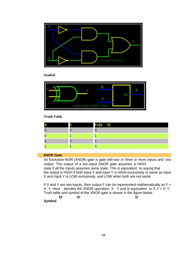
58
Symbol
Truth Table
X Y F=(X Y)
0 0 0
0 1 1
1 0 1
1 1 0
XNOR Gate
An Exclusive-NOR (XNOR) gate is gate with two or three or more inputs and one
output. The output of a two-input XNOR gate assumes a HIGH
state if all the inputs assumes same state. This is equivalent to saying that the output is HIGH if both input X and input Y is HIGH exclusively or same as input X and input Y is LOW exclusively, and LOW when both are not same.
If X and Y are two inputs, then output F can be represented mathematically as F = X Y, Here denotes the XNOR operation. X Y and is equivalent to X.Y + X'.Y'. Truth table and symbol of the XNOR gate is shown in the figure below.
Symbol
59
59
Truth Table
X Y F=(X Y)'
0 0 1
0 1 0
1 0 0
1 1 1
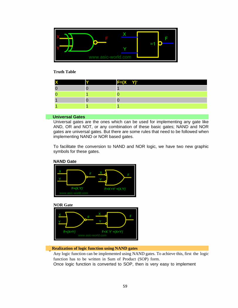
Universal Gates
Universal gates are the ones which can be used for implementing any gate like AND, OR and NOT, or any combination of these basic gates; NAND and NOR gates are universal gates. But there are some rules that need to be followed when implementing NAND or NOR based gates.
To facilitate the conversion to NAND and NOR logic, we have two new graphic symbols for these gates.
NAND Gate
NOR Gate
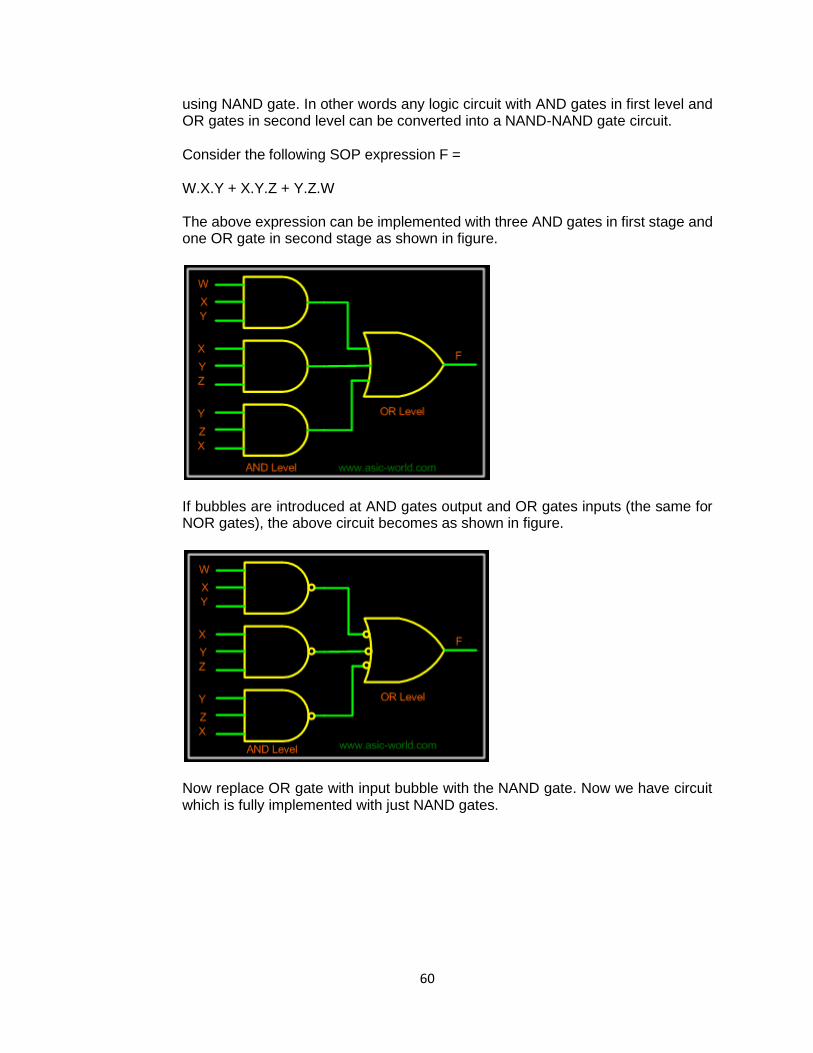
Realization of logic function using NAND gates
Any logic function can be implemented using NAND gates. To achieve this, first the logic
function has to be written in Sum of Product (SOP) form.
Once logic function is converted to SOP, then is very easy to implement
60
60
using NAND gate. In other words any logic circuit with AND gates in first level and OR gates in second level can be converted into a NAND-NAND gate circuit.
Consider the following SOP expression F =
W.X.Y + X.Y.Z + Y.Z.W
The above expression can be implemented with three AND gates in first stage and one OR gate in second stage as shown in figure.
If bubbles are introduced at AND gates output and OR gates inputs (the same for NOR gates), the above circuit becomes as shown in figure.
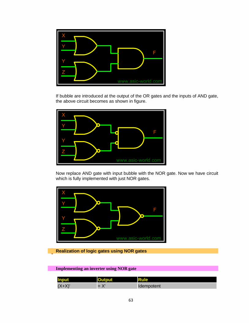
Now replace OR gate with input bubble with the NAND gate. Now we have circuit which is fully implemented with just NAND gates.
61
61
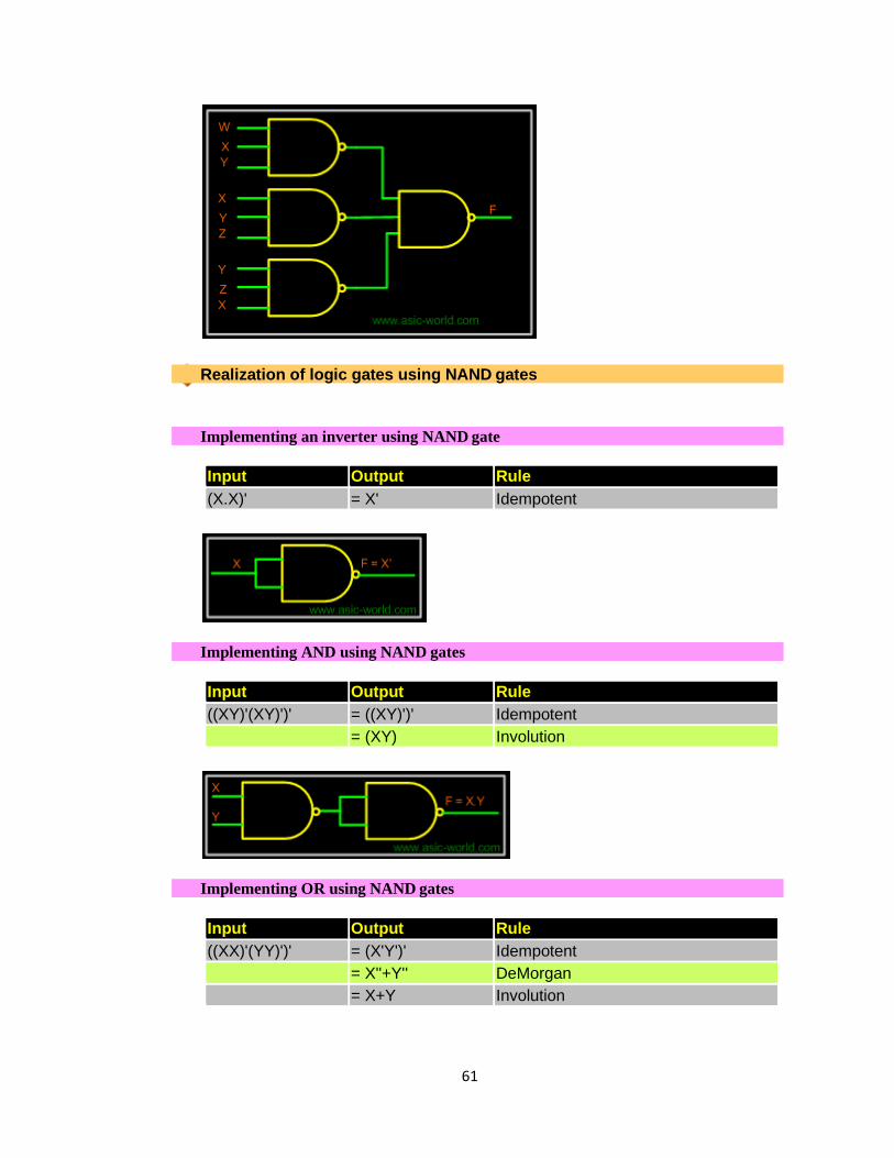
Realization of logic gates using NAND gates
Implementing an inverter using NAND gate
Input Output Rule
(X.X)' = X' Idempotent
Implementing AND using NAND gates
Input Output Rule
((XY)'(XY)')' = ((XY)')' Idempotent
= (XY) Involution
Implementing OR using NAND gates
Input Output Rule
((XX)'(YY)')' = (X'Y')' Idempotent
= X''+Y'' DeMorgan
= X+Y Involution
62
62
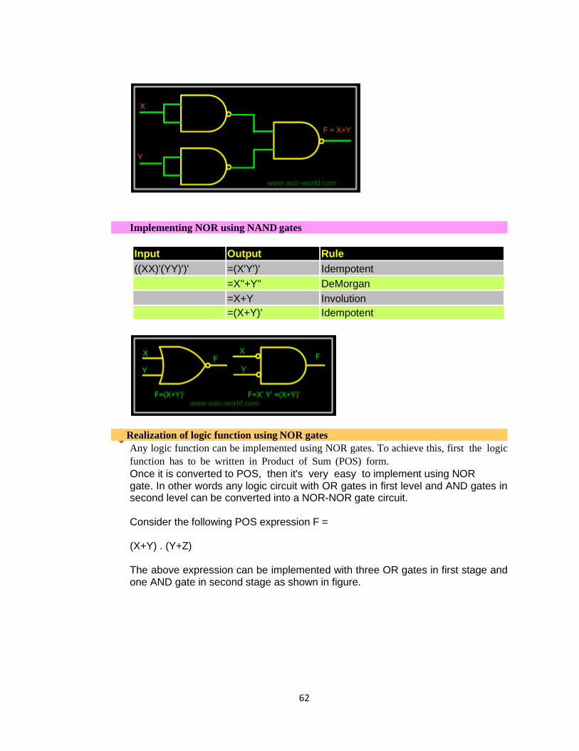
Implementing NOR using NAND gates
Input Output Rule
((XX)'(YY)')' =(X'Y')' Idempotent
=X''+Y'' DeMorgan
=X+Y Involution
=(X+Y)' Idempotent
Realization of logic function using NOR gates
Any logic function can be implemented using NOR gates. To achieve this, first the logic
function has to be written in Product of Sum (POS) form.
Once it is converted to POS, then it's very easy to implement using NOR gate. In other words any logic circuit with OR gates in first level and AND gates in second level can be converted into a NOR-NOR gate circuit.
Consider the following POS expression F =
(X+Y) . (Y+Z)
The above expression can be implemented with three OR gates in first stage and one AND gate in second stage as shown in figure.
63
63
If bubble are introduced at the output of the OR gates and the inputs of AND gate, the above circuit becomes as shown in figure.
Now replace AND gate with input bubble with the NOR gate. Now we have circuit which is fully implemented with just NOR gates.
Realization of logic gates using NOR gates
Implementing an inverter using NOR gate
Input Output Rule
(X+X)' = X' Idempotent
64
64
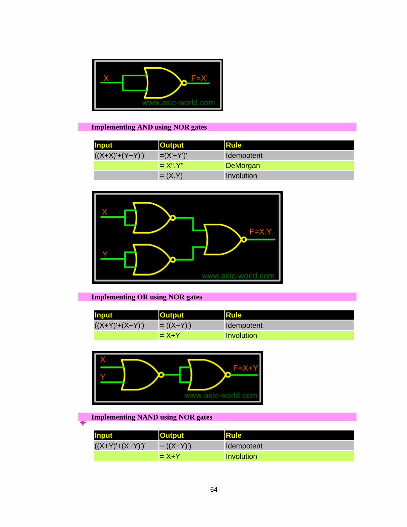
Implementing AND using NOR gates
Input Output Rule
((X+X)'+(Y+Y)')' =(X'+Y')' Idempotent
= X''.Y'' DeMorgan
= (X.Y) Involution
Implementing OR using NOR gates
Input Output Rule
((X+Y)'+(X+Y)')' = ((X+Y)')' Idempotent
= X+Y Involution
Implementing NAND using NOR gates
Input Output Rule
((X+Y)'+(X+Y)')' = ((X+Y)')' Idempotent
= X+Y Involution
65
65
Logic Circuits
Boolean algebra is ideal for expressing the behavior of logic circuits.
A circuit can be expressed as a logic design and implemented as a collection of individual connected logic gates.
Fixed Logic Systems
A fixed logic system has two possible choices for representing true and false.
Positive Logic In a positive logic system, a high voltage is used to represent logical true (1), and a low voltage for a logical false (0).
Negative Logic In a negative logic system, a low voltage is used to represent logical true (1), and a high voltage for a logical false (0).
In positive logic circuits it is normal to use +5V for true and 0V for false.
Switching Circuits
The abstract logic described previously can be implemented as an actual circuit.
Switches are left open for logic 0 and closed for logic 1.
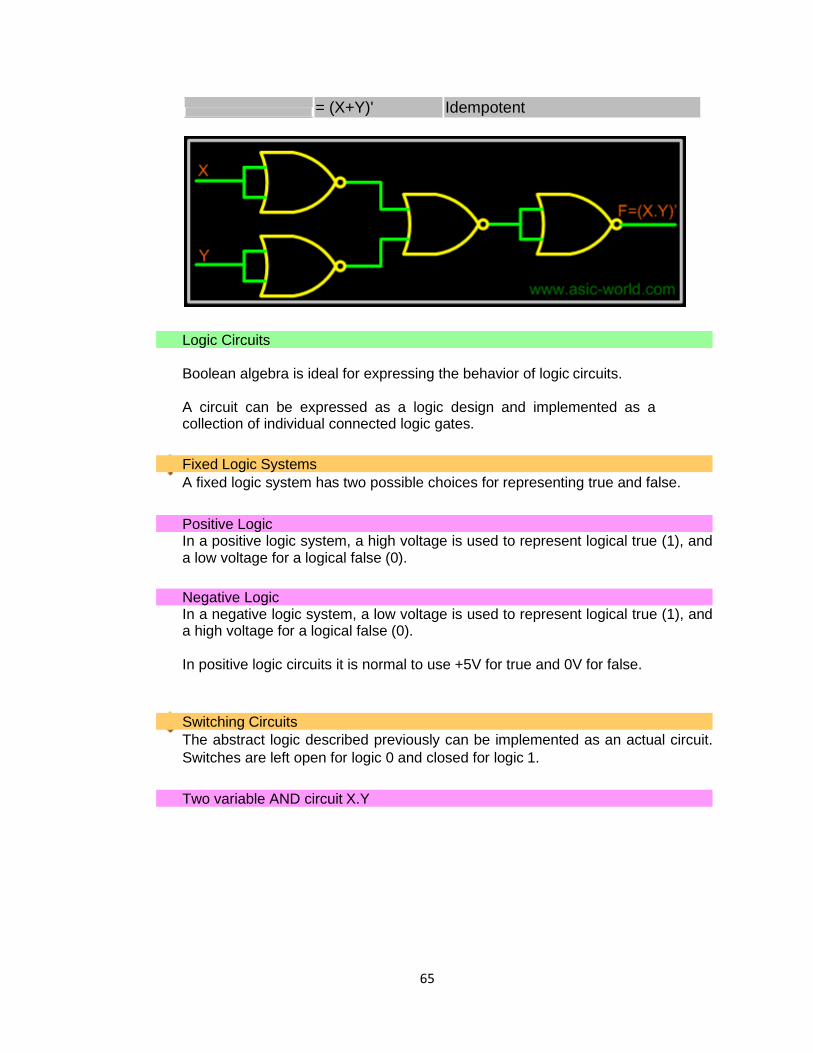
Two variable AND circuit X.Y
= (X+Y)' Idempotent
66
66
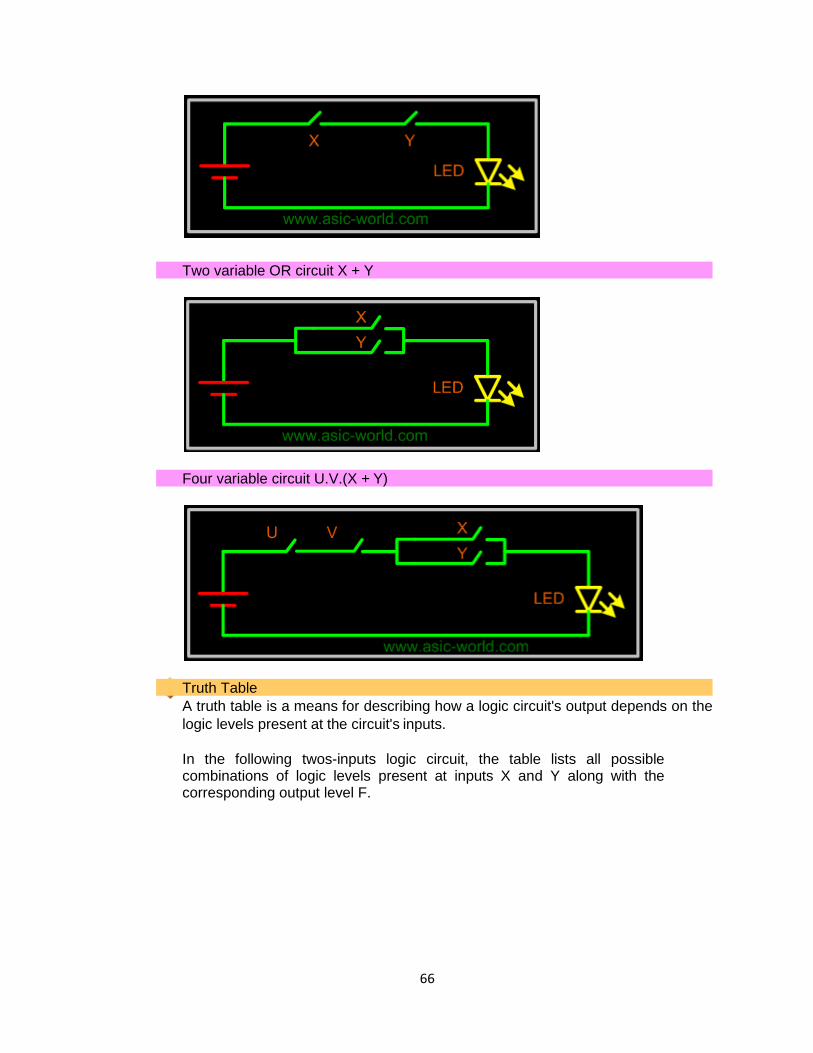
Two variable OR circuit X + Y
Four variable circuit U.V.(X + Y)
Truth Table
A truth table is a means for describing how a logic circuit's output depends on the
logic levels present at the circuit's inputs.
In the following twos-inputs logic circuit, the table lists all possible combinations of logic levels present at inputs X and Y along with the corresponding output level F.
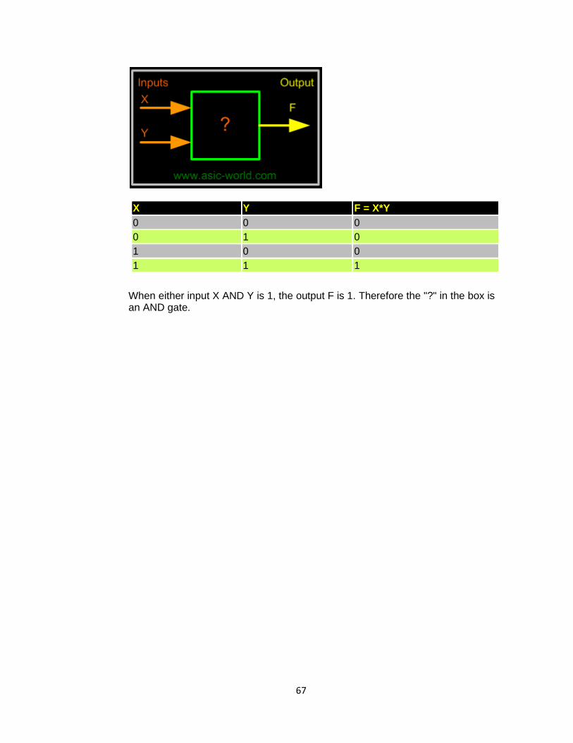
67
67
X Y F = X*Y
0 0 0
0 1 0
1 0 0
1 1 1
When either input X AND Y is 1, the output F is 1. Therefore the "?" in the box is an AND gate.

68
68
Assignment UNIT 1
Academic Year 2020-21
Course : B.Tech.
Semester/
Section : III Sem A
Subject &
Subject
Code
:
Digital Electronics & 3CS3-04
Max. Marks :
20
Course Outcomes
CO1 Apply the principles of number system, binary codes and Boolean algebra to minimize logic
expressions and knowledge about various logic gates
Q.
No. Questions Marks
1. Convert following decimal number into their binary equivalent.
(a) (0.4475)10 (b)(4097.188)10 (c) 167
2
2. Convert following binary number into their decimal equivalent.
(a) 10111.1011 (b) 10001101 (c) 0.011011
2
3. Convert following binary number to octal
(a) 101101110 (b) 110110.011
2
4. Encode following binary digits into 7-bit even parity hamming codes
(a) 1011 (b) 0101 (c) 1000
2
5. Subtract (10110.1)2 from (1100.01)2 2
6. Convert following number into floating point decimal notation
(a) 81200 (b) 0.00379 (c) 89.46
2
7. Perform following division
(a) 111111/1001 (b) 10110.1101/11.1
2
8. Convert following gray code into binary digit
(a) 111011001 (b) 1010101101
2
9. Apply Demorgan theorem
(a) (A+B’+C+D’)’ + (ABCD’)’
2
10. Simplify the following expression
(a) AB’C’+A’B’C’+A’BC’+A’B’C
(b) ABC+A’BC+AB’C+ABC’+AB’C’+A’BC’+A’B’C’
2
69
69
UNIT 2
Minimization techniques
Introduction Simplification of Boolean functions is mainly used to reduce the gate count of a design. Less number of gates means less power consumption, sometimes the circuit works faster and also when number of gates is reduced, cost also comes down.
There are many ways to simplify a logic design, some of them are given below. We will be looking at each of these in detail in the next few pages.
• Algebraic Simplification.
o Simplify symbolically using theorems/postulates. o Requires good skills
• Karnaugh Maps.
o Diagrammatic technique using 'Venn-like diagram'.
o Limited to no more than 6 variables.
We have already seen how Algebraic Simplification works, so lets concentrate on Karnaugh Maps or simply k-maps.
Karnaugh Maps
Karnaugh maps provide a systematic method to obtain simplified sum-of- products (SOPs)
Boolean expressions. This is a compact way of representing a truth table and is a technique
that is used to simplify logic expressions. It is ideally suited for four or less variables,
becoming cumbersome for five or more variables. Each square represents either a minterm or
maxterm. A K-map of n variables will have 2
squares. For a Boolean expression, product terms are denoted by 1's, while sum terms are denoted by 0's - but 0's are often left blank.
A K-map consists of a grid of squares, each square representing one canonical minterm combination of the variables or their inverse. The map is arranged so that squares representing minterms which differ by only one variable are adjacent both vertically and horizontally. Therefore XY'Z' would be adjacent to X'Y'Z' and would also adjacent to XY'Z and XYZ'.
Minimization Technique
• Based on the Unifying Theorem: X + X' = 1 • The expression to be minimized should generally be in sum-of- product form
(If necessary, the conversion process is applied to
70
70
create the sum-of-product form).
• The function is mapped onto the K-map by marking a 1 in those squares corresponding to the terms in the expression to be simplified (The other squares may be filled with 0's).
• Pairs of 1's on the map which are adjacent are combined using the theorem Y(X+X') = Y where Y is any Boolean expression (If two pairs are also adjacent, then these can also be combined using the same theorem).
• The minimization procedure consists of recognizing those pairs and multiple pairs.
o These are circled indicating reduced terms. o Groups which can be circled are those which have two (21) 1's, four (22) 1's,
eight (23) 1's, and so on. o Note that because squares on one edge of the map are considered
adjacent to those on the opposite edge, group can be formed with these squares.
o Groups are allowed to overlap. • The objective is to cover all the 1's on the map in the fewest number of groups
and to create the largest groups to do this. • Once all possible groups have been formed, the corresponding terms are identified.
o A group of two 1's eliminates one variable from the original minterm. o A group of four 1's eliminates two variables from the original minterm. o A group of eight 1's eliminates three variables from the original minterm,
and so on. o The variables eliminated are those which are different in the original
minterms of the group.
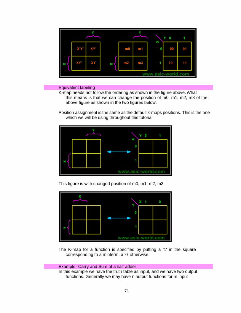
2-Variable K-Map
In any K-Map, each square represents a minterm. Adjacent squares
always differ by just one literal (So that the unifying theorem may apply: X + X' = 1). For the 2-variable case (e.g.: variables X, Y), the map can be drawn as below. Two variable map is the one which has got only two variables as input.
71
71
Equivalent labeling K-map needs not follow the ordering as shown in the figure above. What
this means is that we can change the position of m0, m1, m2, m3 of the above figure as shown in the two figures below.
Position assignment is the same as the default k-maps positions. This is the one
which we will be using throughout this tutorial.
This figure is with changed position of m0, m1, m2, m3.
The K-map for a function is specified by putting a '1' in the square
corresponding to a minterm, a '0' otherwise.
Example- Carry and Sum of a half adder In this example we have the truth table as input, and we have two output
functions. Generally we may have n output functions for m input
72
72
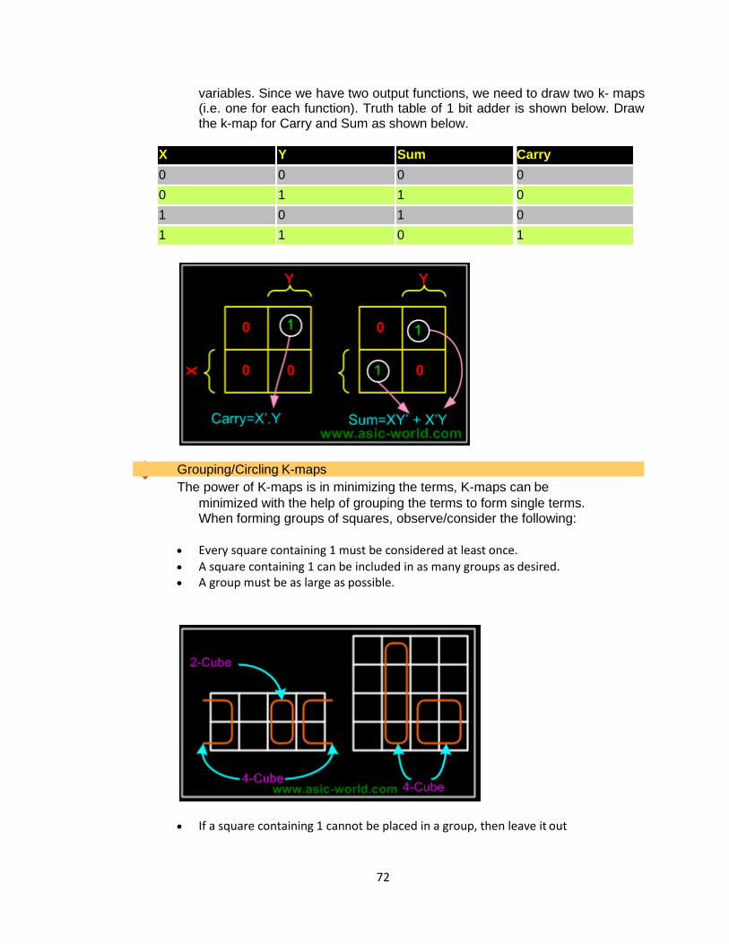
variables. Since we have two output functions, we need to draw two k- maps (i.e. one for each function). Truth table of 1 bit adder is shown below. Draw the k-map for Carry and Sum as shown below.
X Y Sum Carry
0 0 0 0
0 1 1 0
1 0 1 0
1 1 0 1
Grouping/Circling K-maps
The power of K-maps is in minimizing the terms, K-maps can be
minimized with the help of grouping the terms to form single terms. When forming groups of squares, observe/consider the following:
• Every square containing 1 must be considered at least once. • A square containing 1 can be included in as many groups as desired. • A group must be as large as possible.
• If a square containing 1 cannot be placed in a group, then leave it out
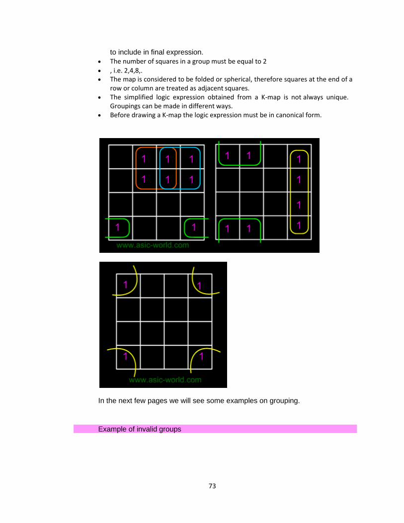
73
73
to include in final expression.
• The number of squares in a group must be equal to 2
• , i.e. 2,4,8,. • The map is considered to be folded or spherical, therefore squares at the end of a
row or column are treated as adjacent squares. • The simplified logic expression obtained from a K-map is not always unique.
Groupings can be made in different ways. • Before drawing a K-map the logic expression must be in canonical form.
In the next few pages we will see some examples on grouping.
Example of invalid groups
74
74
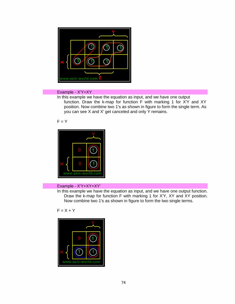
Example - X'Y+XY In this example we have the equation as input, and we have one output
function. Draw the k-map for function F with marking 1 for X'Y and XY position. Now combine two 1's as shown in figure to form the single term. As you can see X and X' get canceled and only Y remains.
F = Y
Example - X'Y+XY+XY'
In this example we have the equation as input, and we have one output function. Draw the k-map for function F with marking 1 for X'Y, XY and XY position. Now combine two 1's as shown in figure to form the two single terms.
F = X + Y

75
75
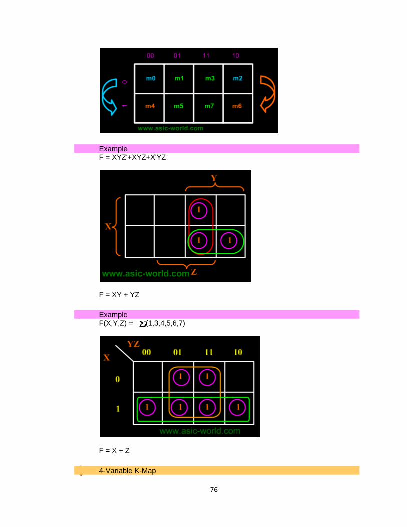
3-Variable K-Map
There are 8 minterms for 3 variables (X, Y, Z). Therefore, there are 8
cells in a 3-variable K-map. One important thing to note is that K-
maps follow the gray code sequence, not the binary one.
Using gray code arrangement ensures that minterms of adjacent cells differ
by only ONE literal. (Other arrangements which satisfy this criterion may also be used.)
Each cell in a 3-variable K-map has 3 adjacent neighbours. In general, each
cell in an n-variable K-map has n adjacent neighbours.
There is wrap-around in the K-map
• X'Y'Z' (m0) is adjacent to X'YZ' (m2) • XY'Z' (m4) is adjacent to XYZ' (m6)
76
76
Example F = XYZ'+XYZ+X'YZ
F = XY + YZ
Example F(X,Y,Z) = (1,3,4,5,6,7)
F = X + Z
4-Variable K-Map
77
77
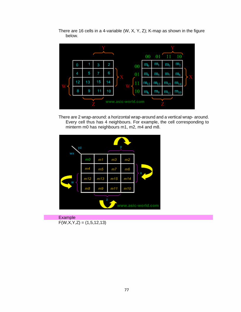
There are 16 cells in a 4-variable (W, X, Y, Z); K-map as shown in the figure below.
There are 2 wrap-around: a horizontal wrap-around and a vertical wrap- around.
Every cell thus has 4 neighbours. For example, the cell corresponding to minterm m0 has neighbours m1, m2, m4 and m8.
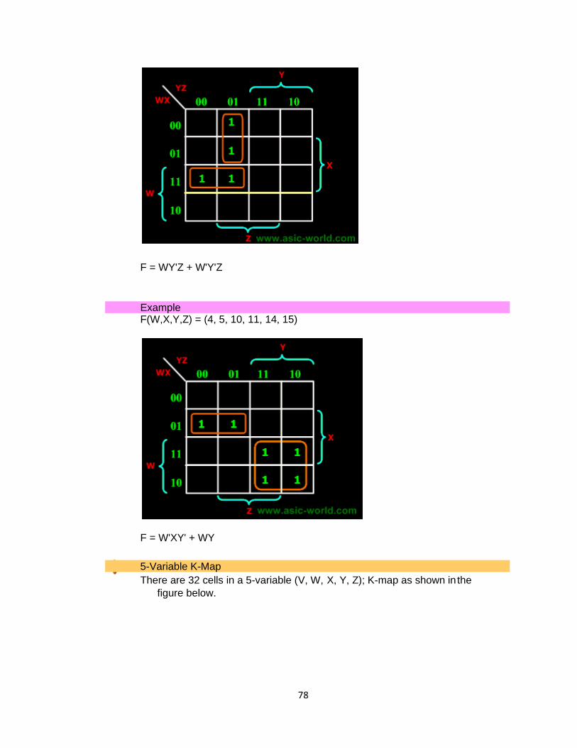
Example
F(W,X,Y,Z) = (1,5,12,13)
78
78
F = WY'Z + W'Y'Z
Example F(W,X,Y,Z) = (4, 5, 10, 11, 14, 15)
F = W'XY' + WY
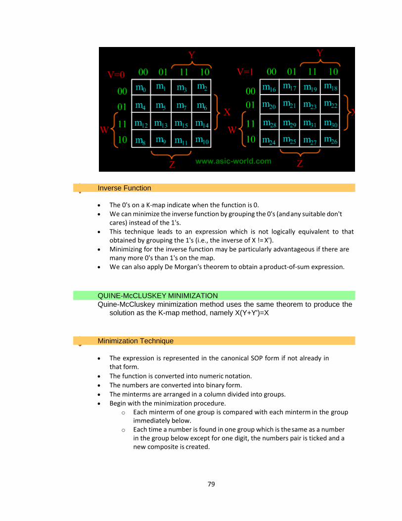
5-Variable K-Map
There are 32 cells in a 5-variable (V, W, X, Y, Z); K-map as shown in the
figure below.
79
79
Inverse Function
• The 0's on a K-map indicate when the function is 0. • We can minimize the inverse function by grouping the 0's (and any suitable don't
cares) instead of the 1's. • This technique leads to an expression which is not logically equivalent to that
obtained by grouping the 1's (i.e., the inverse of X != X'). • Minimizing for the inverse function may be particularly advantageous if there are
many more 0's than 1's on the map. • We can also apply De Morgan's theorem to obtain a product-of-sum expression.
QUINE-McCLUSKEY MINIMIZATION
Quine-McCluskey minimization method uses the same theorem to produce the solution as the K-map method, namely X(Y+Y')=X
Minimization Technique
• The expression is represented in the canonical SOP form if not already in
that form.
• The function is converted into numeric notation.
• The numbers are converted into binary form.
• The minterms are arranged in a column divided into groups. • Begin with the minimization procedure.
o Each minterm of one group is compared with each minterm in the group immediately below.
o Each time a number is found in one group which is the same as a number in the group below except for one digit, the numbers pair is ticked and a new composite is created.
80
80
o This composite number has the same number of digits as the numbers in the pair except the digit different which is replaced by an "x".
• The above procedure is repeated on the second column to generate a third column. • The next step is to identify the essential prime implicants, which can be done
using a prime implicant chart. o Where a prime implicant covers a minterm, the intersection of the
corresponding row and column is marked with a cross. o Those columns with only one cross identify the essential prime implicants.
-> These prime implicants must be in the final answer. o The single crosses on a column are circled and all the crosses on the same
row are also circled, indicating that these crosses are covered by the prime implicants selected.
o Once one cross on a column is circled, all the crosses on that column can be circled since the minterm is now covered.
o If any non-essential prime implicant has all its crosses circled, the prime implicant is redundant and need not be considered further.
• Next, a selection must be made from the remaining nonessential prime implicants, by considering how the non-circled crosses can be covered best.
o One generally would take those prime implicants which cover the greatest number of crosses on their row.
o If all the crosses in one row also occur on another row which includes further crosses, then the latter is said to dominate the former and can be selected.
o The dominated prime implicant can then be deleted.
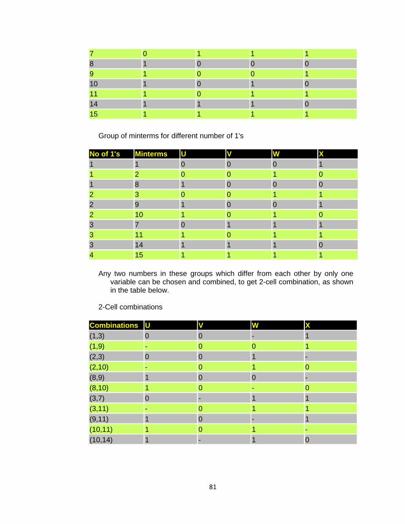
Example Find the minimal sum of products for the Boolean expression, f=
(1,2,3,7,8,9,10,11,14,15), using Quine-McCluskey method.
Firstly these minterms are represented in the binary form as shown in the table
below. The above binary representations are grouped into a number of sections in terms of the number of 1's as shown in the table below.
Binary representation of minterms
Minterms U V W X
1 0 0 0 1
2 0 0 1 0
3 0 0 1 1
81
81
7 0 1 1 1
8 1 0 0 0
9 1 0 0 1
10 1 0 1 0
11 1 0 1 1
14 1 1 1 0
15 1 1 1 1
Group of minterms for different number of 1's
No of 1's Minterms U V W X
1 1 0 0 0 1
1 2 0 0 1 0
1 8 1 0 0 0
2 3 0 0 1 1
2 9 1 0 0 1
2 10 1 0 1 0
3 7 0 1 1 1
3 11 1 0 1 1
3 14 1 1 1 0
4 15 1 1 1 1
Any two numbers in these groups which differ from each other by only one
variable can be chosen and combined, to get 2-cell combination, as shown in the table below.
2-Cell combinations
Combinations U V W X
(1,3) 0 0 - 1
(1,9) - 0 0 1
(2,3) 0 0 1 -
(2,10) - 0 1 0
(8,9) 1 0 0 -
(8,10) 1 0 - 0
(3,7) 0 - 1 1
(3,11) - 0 1 1
(9,11) 1 0 - 1
(10,11) 1 0 1 -
(10,14) 1 - 1 0
82
82
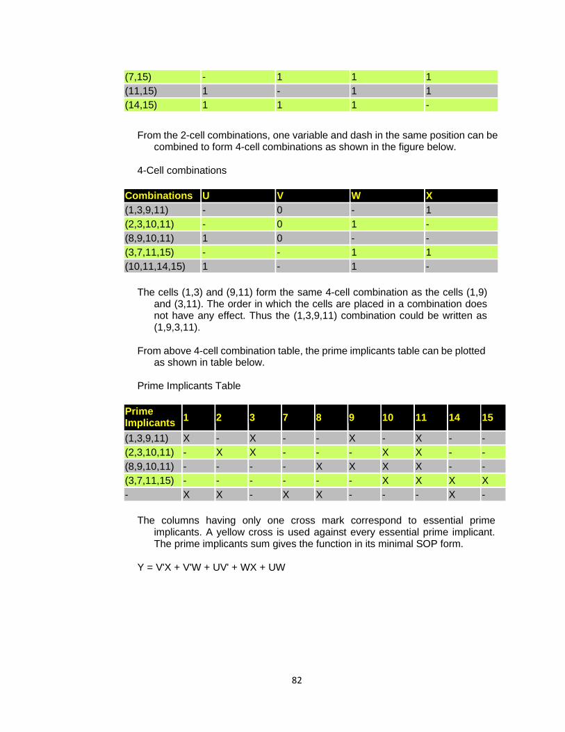
(7,15) - 1 1 1
(11,15) 1 - 1 1
(14,15) 1 1 1 -
From the 2-cell combinations, one variable and dash in the same position can be combined to form 4-cell combinations as shown in the figure below.
4-Cell combinations
Combinations U V W X
(1,3,9,11) - 0 - 1
(2,3,10,11) - 0 1 -
(8,9,10,11) 1 0 - -
(3,7,11,15) - - 1 1
(10,11,14,15) 1 - 1 -
The cells (1,3) and (9,11) form the same 4-cell combination as the cells (1,9)
and (3,11). The order in which the cells are placed in a combination does not have any effect. Thus the (1,3,9,11) combination could be written as (1,9,3,11).
From above 4-cell combination table, the prime implicants table can be plotted
as shown in table below.
Prime Implicants Table
Prime Implicants
1 2 3 7 8 9 10 11 14 15
(1,3,9,11) X - X - - X - X - -
(2,3,10,11) - X X - - - X X - -
(8,9,10,11) - - - - X X X X - -
(3,7,11,15) - - - - - - X X X X
- X X - X X - - - X -
The columns having only one cross mark correspond to essential prime
implicants. A yellow cross is used against every essential prime implicant. The prime implicants sum gives the function in its minimal SOP form.
Y = V'X + V'W + UV' + WX + UW

83
83
Assignment UNIT 2
Academic Year 2020-21
Course : B.Tech.
Semester/
Section
: III Sem A
Subject &
Subject Code
: Digital Electronics & 3CS3-04 Max. Marks : 20
Course Outcomes
CO2
Develop K-maps and apply Quine Mc Cluskey’s method to minimize and optimize logic functions
up to 4 variables
Q.
No.
Questions Marks
1. Convert the given Boolean expression into standard SOP form. Y= A+ B’C’+ ABC 2
2. Convert the given Boolean expression into standard POS form. Y= (A+C)B’ 2
3. Convert the given POS expression into SOP form: Y= (A+B’)(B’+C’) 2
4. Convert the given POS expression into SOP form and draw its truth table: Y=
(A+B+C’)(A’+C)
2
5. Simplify the given Boolean expression using K-map Y= ∑m (4,5,8,9,12,13,14,15) 2
6. Solve for POS expression using K-Map- Y= πM (1,2,3,5,8,10,11,12,14) 2
7. Simplify the given Boolean expression using K-map Y= ∑m (2,3,4,7,10,12,13,15)
+d(6,8)
2
8. Solve for POS expression using K-Map- Y= πM (0,3,4,5,8,9,11) + d(1,15) 2
9. Design truth table for the given Boolean expression: Y= AC’+B’ 2
10. Simplify using Quine Mc Cluskey’s method: Y= ∑m (0,1,2,4,5,6,9,12,15) + d(3,14) 2

84
84
UNIT-3
Digital Logic Families
Digital Logic Families.
Logic families can be classified broadly according to the technologies they are built with.
In earlier days we had vast number of these technologies, as you can see in the list below.
• DL : Diode Logic.
• RTL : Resistor Transistor Logic.
• DTL : Diode Transistor Logic.
• HTL : High threshold Logic. • TTL : Transistor Transistor Logic. • I2L : Integrated Injection Logic. • ECL : Emitter coupled logic.
• MOS : Metal Oxide Semiconductor Logic (PMOS and NMOS). • CMOS : Complementary Metal Oxide Semiconductor Logic.
Among these, only CMOS is most widely used by the ASIC (Chip) designers; we will still try to understand a few of the extinct / less used technologies. More in-depth explanation of CMOS will be covered in the VLSI section.
Basic Concepts
Before we start looking at the how gates are built using various technologies, we need to understand a few basic concepts. These concepts will go long way i.e. if you become a ASIC designer or Board designer, you may need to know these concepts very well.
• Fan-in.
• Fan-out. • Noise Margin. • Power Dissipation.
• Gate Delay.
• Wire Delay. • Skew.
85
85
• Voltage Threshold.
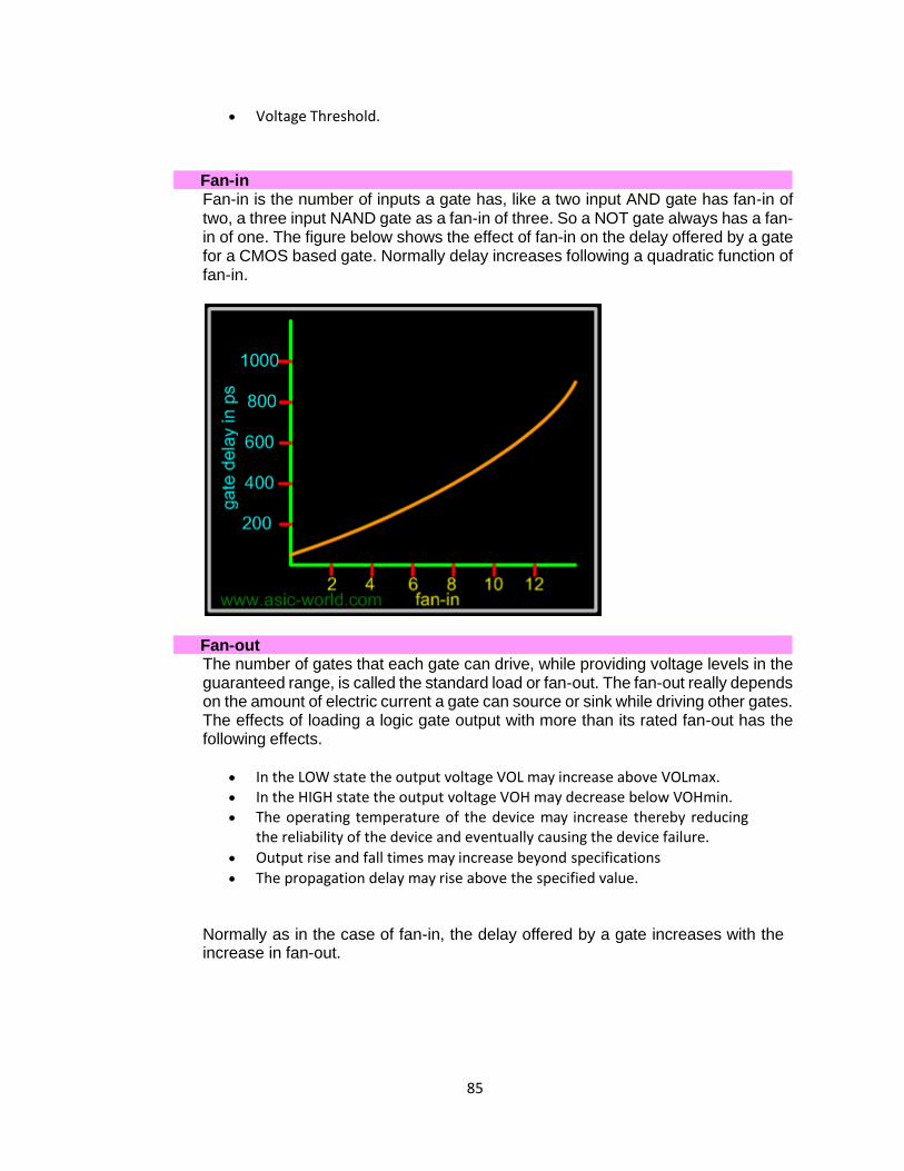
Fan-in Fan-in is the number of inputs a gate has, like a two input AND gate has fan-in of two, a three input NAND gate as a fan-in of three. So a NOT gate always has a fan-in of one. The figure below shows the effect of fan-in on the delay offered by a gate for a CMOS based gate. Normally delay increases following a quadratic function of fan-in.
Fan-out
The number of gates that each gate can drive, while providing voltage levels in the guaranteed range, is called the standard load or fan-out. The fan-out really depends on the amount of electric current a gate can source or sink while driving other gates. The effects of loading a logic gate output with more than its rated fan-out has the following effects.
• In the LOW state the output voltage VOL may increase above VOLmax. • In the HIGH state the output voltage VOH may decrease below VOHmin. • The operating temperature of the device may increase thereby reducing
the reliability of the device and eventually causing the device failure.
• Output rise and fall times may increase beyond specifications • The propagation delay may rise above the specified value.
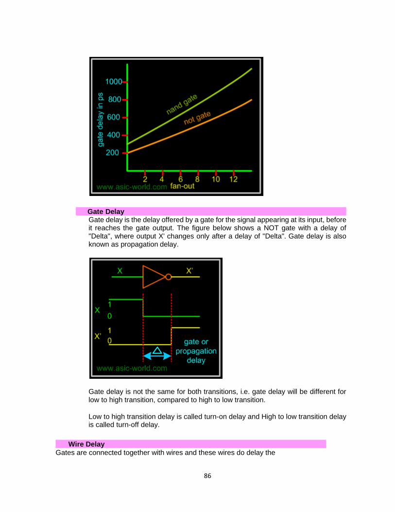
Normally as in the case of fan-in, the delay offered by a gate increases with the increase in fan-out.
86
86
Gate Delay Gate delay is the delay offered by a gate for the signal appearing at its input, before it reaches the gate output. The figure below shows a NOT gate with a delay of "Delta", where output X' changes only after a delay of "Delta". Gate delay is also known as propagation delay.
Gate delay is not the same for both transitions, i.e. gate delay will be different for low to high transition, compared to high to low transition.
Low to high transition delay is called turn-on delay and High to low transition delay is called turn-off delay.
Wire Delay
Gates are connected together with wires and these wires do delay the
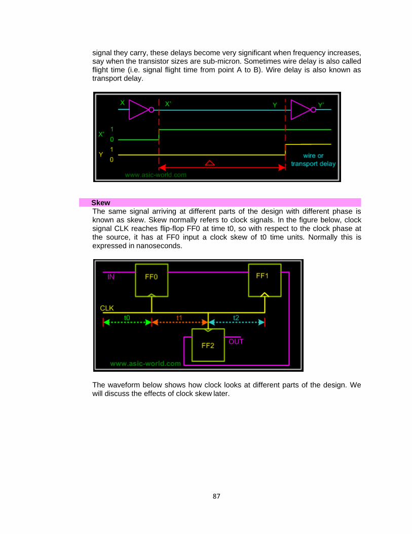
87
87
signal they carry, these delays become very significant when frequency increases, say when the transistor sizes are sub-micron. Sometimes wire delay is also called flight time (i.e. signal flight time from point A to B). Wire delay is also known as transport delay.
Skew The same signal arriving at different parts of the design with different phase is known as skew. Skew normally refers to clock signals. In the figure below, clock signal CLK reaches flip-flop FF0 at time t0, so with respect to the clock phase at the source, it has at FF0 input a clock skew of t0 time units. Normally this is expressed in nanoseconds.
The waveform below shows how clock looks at different parts of the design. We will discuss the effects of clock skew later.
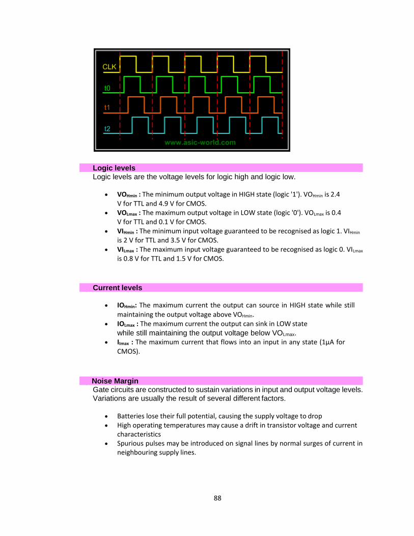
88
88
Logic levels
Logic levels are the voltage levels for logic high and logic low.
• VOHmin : The minimum output voltage in HIGH state (logic '1'). VOHmin is 2.4
V for TTL and 4.9 V for CMOS. • VOLmax : The maximum output voltage in LOW state (logic '0'). VOLmax is 0.4
V for TTL and 0.1 V for CMOS. • VIHmin : The minimum input voltage guaranteed to be recognised as logic 1. VIHmin
is 2 V for TTL and 3.5 V for CMOS. • VILmax : The maximum input voltage guaranteed to be recognised as logic 0. VILmax
is 0.8 V for TTL and 1.5 V for CMOS.
Current levels
• IOHmin: The maximum current the output can source in HIGH state while still maintaining the output voltage above VOHmin.
• IOLmax : The maximum current the output can sink in LOW state
while still maintaining the output voltage below VOLmax.
• IImax : The maximum current that flows into an input in any state (1µA for
CMOS).
Noise Margin Gate circuits are constructed to sustain variations in input and output voltage levels. Variations are usually the result of several different factors.
• Batteries lose their full potential, causing the supply voltage to drop • High operating temperatures may cause a drift in transistor voltage and current
characteristics • Spurious pulses may be introduced on signal lines by normal surges of current in
neighbouring supply lines.
89
89
All these undesirable voltage variations that are superimposed on normal operating voltage levels are called noise. All gates are designed to tolerate a certain amount of noise on their input and output ports. The maximum noise voltage level that is tolerated by a gate is called noise margin. It derives from I/P-O/P voltage characteristic, measured under different operating conditions. It's normally supplied from manufacturer in the gate documentation.
• LNM (Low noise margin): The largest noise amplitude that is guaranteed
not to change the output voltage level when superimposed on the input voltage of the logic gate (when this voltage is in the LOW interval). LNM=VILmax-VOLmax.
• HNM (High noise margin): The largest noise amplitude that is guaranteed not to change the output voltage level if superimposed on the input voltage of the logic gate (when this voltage is in the HIGH interval). HNM=VOHmin-VIHmin
tr (Rise time)
The time required for the output voltage to increase from VILmax to VIHmin.
tf (Fall time)
The time required for the output voltage to decrease from VIHmin to VILmax.
tp (Propagation delay)
The time between the logic transition on an input and the corresponding logic transition on
the output of the logic gate. The propagation delay is measured at midpoints.
Power Dissipation. Each gate is connected to a power supply VCC (VDD in the case of CMOS). It draws a certain amount of current during its operation. Since each gate can be in a High, Transition or Low state, there are three different currents drawn from power supply.
• ICCH: Current drawn during HIGH state.
• ICCT: Current drawn during HIGH to LOW, LOW to HIGH transition. • ICCL: Current drawn during LOW state.
For TTL, ICCT the transition current is negligible, in comparison to ICCH and ICCL. If we assume that ICCH and ICCL are equal then,
Average Power Dissipation = Vcc * (ICCH + ICCL)/2
90
90
For CMOS, ICCH and ICCL current is negligible, in comparison to ICCT. So the Average power dissipation is calculated as below.
Average Power Dissipation = Vcc * ICCT.
So for TTL like logics family, power dissipation does not depend on frequency of operation, and for CMOS the power dissipation depends on the operation frequency.
Power Dissipation is an important metric for two reasons. The amount of current and power available in a battery is nearly constant. Power dissipation of a circuit or system defines battery life: the greater the power dissipation, the shorter the battery life. Power dissipation is proportional to the heat generated by the chip or system; excessive heat dissipation may increase operating temperature and cause gate circuitry to drift out of its normal operating range; will cause gates to generate improper output values. Thus power dissipation of any gate implementation must be kept as low as possible.
Moreover, power dissipation can be classified into Static power dissipation and Dynamic power dissipation.
• Ps (Static Power Dissipation): Power consumed when the output or input are
not changing or rather when clock is turned off. Normally static power dissipation is caused by leakage current. (As we reduce the transistor size, i.e. below 90nm, leakage current could be as high as 40% of total power dissipation).
• Pd (Dynamic Power Dissipation): Power consumed during output and input transitions. So we can say Pd is the actual power consumed i.e. the power consumed by transistors + leakage current.
Thus
Total power dissipation = static power dissipation + dynamic power dissipation.
Diode Logic
In DL (diode logic), all the logic is implemented using diodes and resistors. One
basic thing about the diode, is that diode needs to be forward biased to conduct.
Below is the example of a few DL logic circuits.
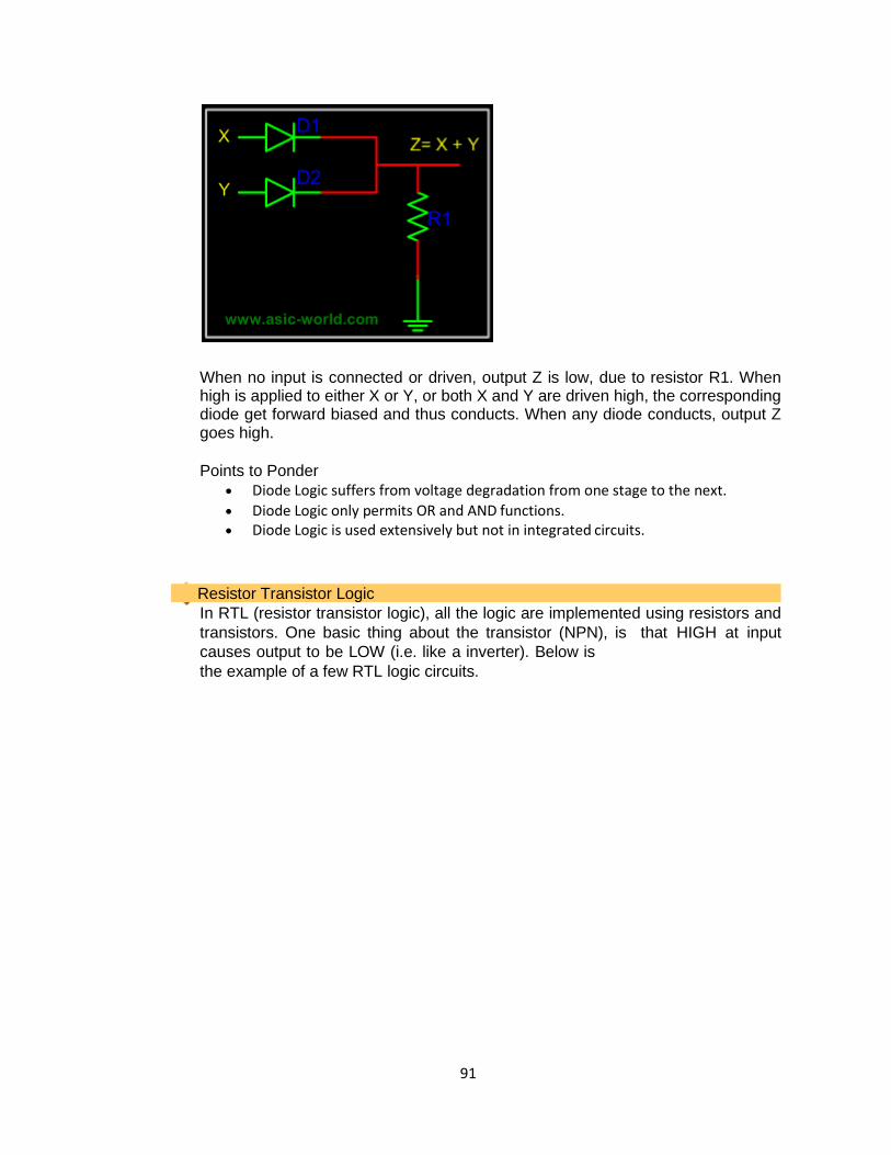
91
91
When no input is connected or driven, output Z is low, due to resistor R1. When high is applied to either X or Y, or both X and Y are driven high, the corresponding diode get forward biased and thus conducts. When any diode conducts, output Z goes high.
Points to Ponder
• Diode Logic suffers from voltage degradation from one stage to the next.
• Diode Logic only permits OR and AND functions. • Diode Logic is used extensively but not in integrated circuits.
Resistor Transistor Logic
In RTL (resistor transistor logic), all the logic are implemented using resistors and
transistors. One basic thing about the transistor (NPN), is that HIGH at input
causes output to be LOW (i.e. like a inverter). Below is
the example of a few RTL logic circuits.
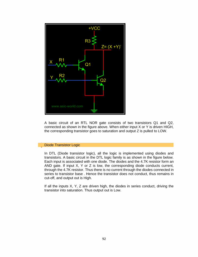
92
92
A basic circuit of an RTL NOR gate consists of two transistors Q1 and Q2, connected as shown in the figure above. When either input X or Y is driven HIGH, the corresponding transistor goes to saturation and output Z is pulled to LOW.
Diode Transistor Logic
In DTL (Diode transistor logic), all the logic is implemented using diodes and transistors. A basic circuit in the DTL logic family is as shown in the figure below. Each input is associated with one diode. The diodes and the 4.7K resistor form an AND gate. If input X, Y or Z is low, the corresponding diode conducts current, through the 4.7K resistor. Thus there is no current through the diodes connected in series to transistor base . Hence the transistor does not conduct, thus remains in cut-off, and output out is High.
If all the inputs X, Y, Z are driven high, the diodes in series conduct, driving the transistor into saturation. Thus output out is Low.

93
93
Transistor Transistor Logic
In Transistor Transistor logic or just TTL, logic gates are built only around
transistors. TTL was developed in 1965. Through the years basic TTL has
been improved to meet performance requirements. There are many
versions or families of TTL.
• Standard TTL.
• High Speed TTL • Low Power TTL. • Schhottky TTL.
Here we will discuss only basic TTL as of now; maybe in the future I will add more details about other TTL versions. As such all TTL families have three configurations for outputs.
• Totem - Pole output. • Open Collector Output. • Tristate Output.
Before we discuss the output stage let's look at the input stage, which is used with almost all versions of TTL. This consists of an input transistor and a phase splitter transistor. Input stage consists of a multi emitter transistor as shown in the figure below. When any input is driven low, the emitter base junction is forward biased and input transistor conducts. This in turn drives the phase splitter transistor into cut-off.
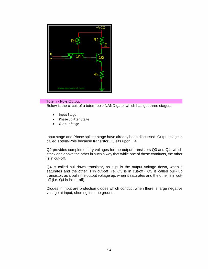
94
94
Totem - Pole Output Below is the circuit of a totem-pole NAND gate, which has got three stages.
• Input Stage • Phase Splitter Stage • Output Stage
Input stage and Phase splitter stage have already been discussed. Output stage is called Totem-Pole because transistor Q3 sits upon Q4.
Q2 provides complementary voltages for the output transistors Q3 and Q4, which stack one above the other in such a way that while one of these conducts, the other is in cut-off.
Q4 is called pull-down transistor, as it pulls the output voltage down, when it saturates and the other is in cut-off (i.e. Q3 is in cut-off). Q3 is called pull- up transistor, as it pulls the output voltage up, when it saturates and the other is in cut-off (i.e. Q4 is in cut-off).
Diodes in input are protection diodes which conduct when there is large negative voltage at input, shorting it to the ground.
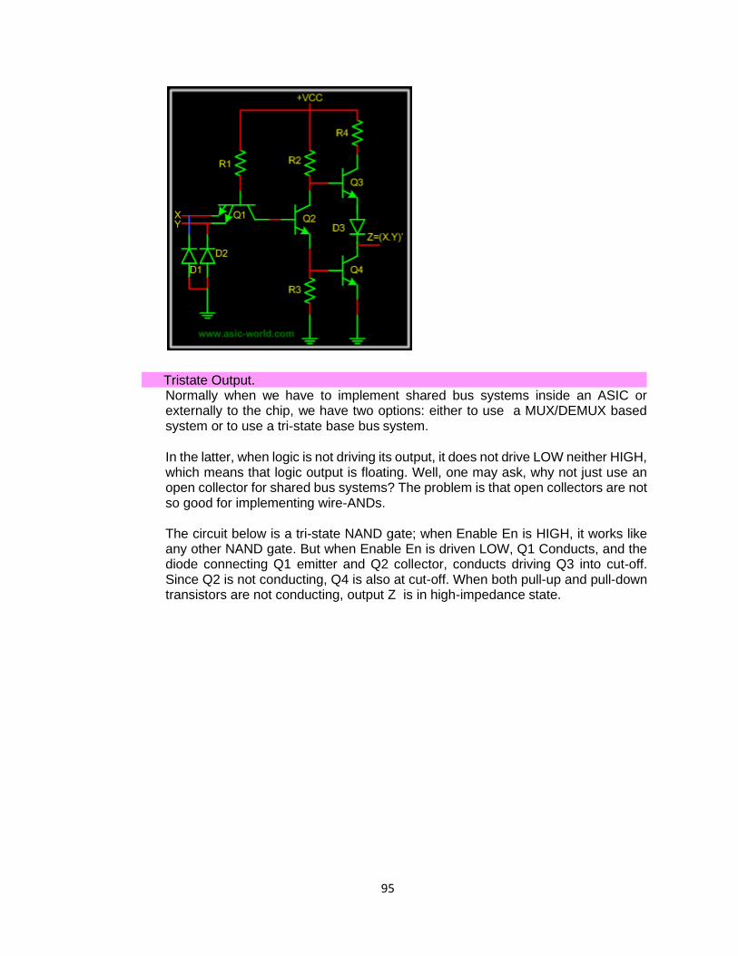
95
95
Tristate Output. Normally when we have to implement shared bus systems inside an ASIC or externally to the chip, we have two options: either to use a MUX/DEMUX based system or to use a tri-state base bus system.
In the latter, when logic is not driving its output, it does not drive LOW neither HIGH, which means that logic output is floating. Well, one may ask, why not just use an open collector for shared bus systems? The problem is that open collectors are not so good for implementing wire-ANDs.
The circuit below is a tri-state NAND gate; when Enable En is HIGH, it works like any other NAND gate. But when Enable En is driven LOW, Q1 Conducts, and the diode connecting Q1 emitter and Q2 collector, conducts driving Q3 into cut-off. Since Q2 is not conducting, Q4 is also at cut-off. When both pull-up and pull-down transistors are not conducting, output Z is in high-impedance state.
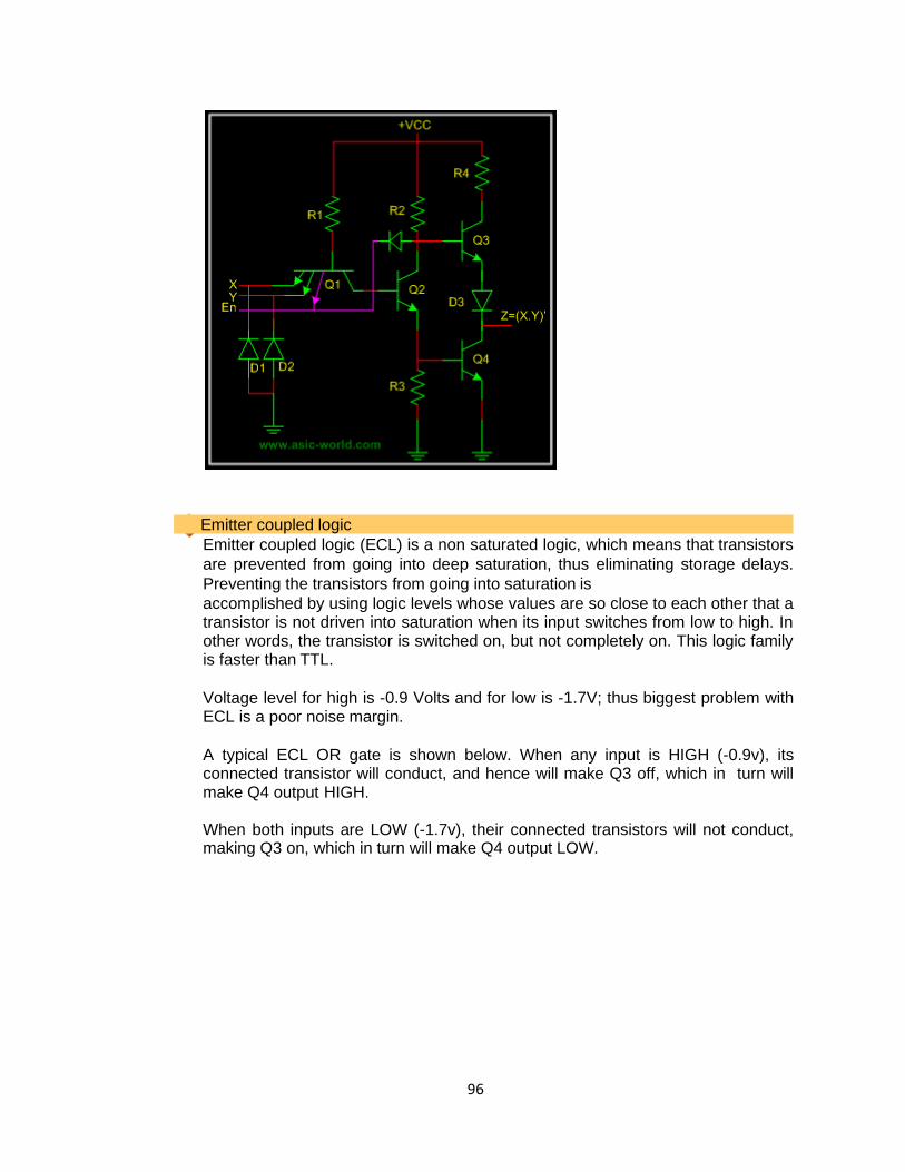
96
96
Emitter coupled logic
Emitter coupled logic (ECL) is a non saturated logic, which means that transistors
are prevented from going into deep saturation, thus eliminating storage delays.
Preventing the transistors from going into saturation is
accomplished by using logic levels whose values are so close to each other that a transistor is not driven into saturation when its input switches from low to high. In other words, the transistor is switched on, but not completely on. This logic family is faster than TTL.
Voltage level for high is -0.9 Volts and for low is -1.7V; thus biggest problem with ECL is a poor noise margin.
A typical ECL OR gate is shown below. When any input is HIGH (-0.9v), its connected transistor will conduct, and hence will make Q3 off, which in turn will make Q4 output HIGH.
When both inputs are LOW (-1.7v), their connected transistors will not conduct, making Q3 on, which in turn will make Q4 output LOW.

97
97
Metal Oxide Semiconductor Logic
MOS or Metal Oxide Semiconductor logic uses nmos and pmos to implement logic
gates. One needs to know the operation of FET and MOS transistors to understand
the operation of MOS logic circuits.
The basic NMOS inverter is shown below: when input is LOW, NMOS transistor does not conduct, and thus output is HIGH. But when input is HIGH, NMOS transistor conducts and thus output is LOW.
Normally it is difficult to fabricate resistors inside the chips, so the resistor is replaced with an NMOS gate as shown below. This new NMOS transistor acts as resistor.
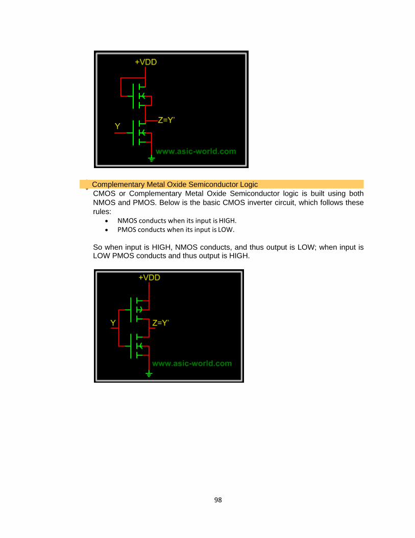
98
98
Complementary Metal Oxide Semiconductor Logic
CMOS or Complementary Metal Oxide Semiconductor logic is built using both
NMOS and PMOS. Below is the basic CMOS inverter circuit, which follows these
rules:
• NMOS conducts when its input is HIGH. • PMOS conducts when its input is LOW.
So when input is HIGH, NMOS conducts, and thus output is LOW; when input is LOW PMOS conducts and thus output is HIGH.

99
99
Assignment UNIT 3
Academic Year 2020-21
Course : B.Tech.
Semester/
Section
: III Sem A
Subject &
Subject Code
: Digital Electronics & 3CS3-04 Max. Marks : 20
Course Outcomes
CO3
Acquire knowledge about various logic families and analyze basic logic gate circuits of these
families.
Q.
No.
Questions Marks
1. Write characteristics of digital IC 2
2. Explain working of TTL NAND gate totem pole output configuration with the help of
suitable diagram.
2
3. Design RTL NOR gate and explain its working. 2
4. Design NMOS nand gate and explain its working. 2
5. Explain the working of pmos nand gate with the help of suitable diagram. 2
6. Explain working of ECL nor/or gate. 2
7. Design DTL NAND gate. 2
8. Design CMOS NOR gate. 2
9. Design CMOS XOR gate. 2
10. Elaborate the TTL logic families 2

100
100
UNIT-4
Combinational circuits
Introduction Arithmetic circuits are the ones which perform arithmetic operations like addition, subtraction, multiplication, division, parity calculation. Most of the time, designing these circuits is the same as designing muxers, encoders and decoders.
Adders Adders are the basic building blocks of all arithmetic circuits; adders add two binary numbers and give out sum and carry as output. Basically we have two types of adders.
• Half Adder. • Full Adder.
Half Adder
Adding two single-bit binary values X, Y produces a sum S bit and a carry out C-out bit. This
operation is called half addition and the circuit to realize it
is called a half adder.
Truth Table
X Y SUM CARRY
0 0 0 0
0 1 1 0
1 0 1 0
1 1 0 1
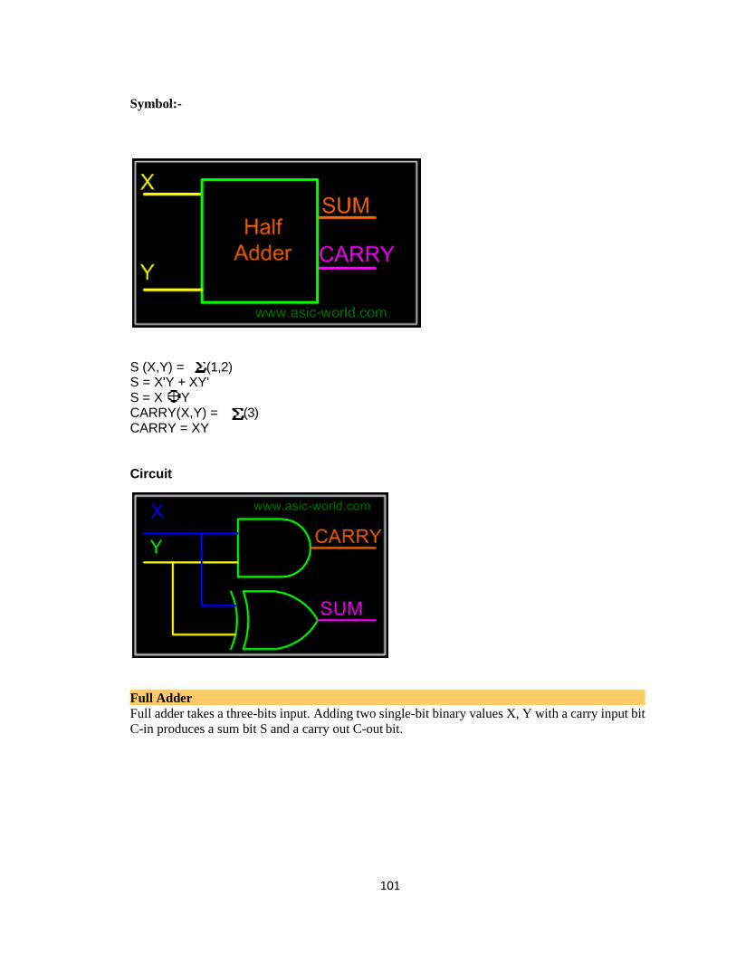
101
101
Symbol:-
S (X,Y) = (1,2) S = X'Y + XY' S = X Y CARRY(X,Y) = (3) CARRY = XY
Circuit
Full Adder
Full adder takes a three-bits input. Adding two single-bit binary values X, Y with a carry input bit
C-in produces a sum bit S and a carry out C-out bit.
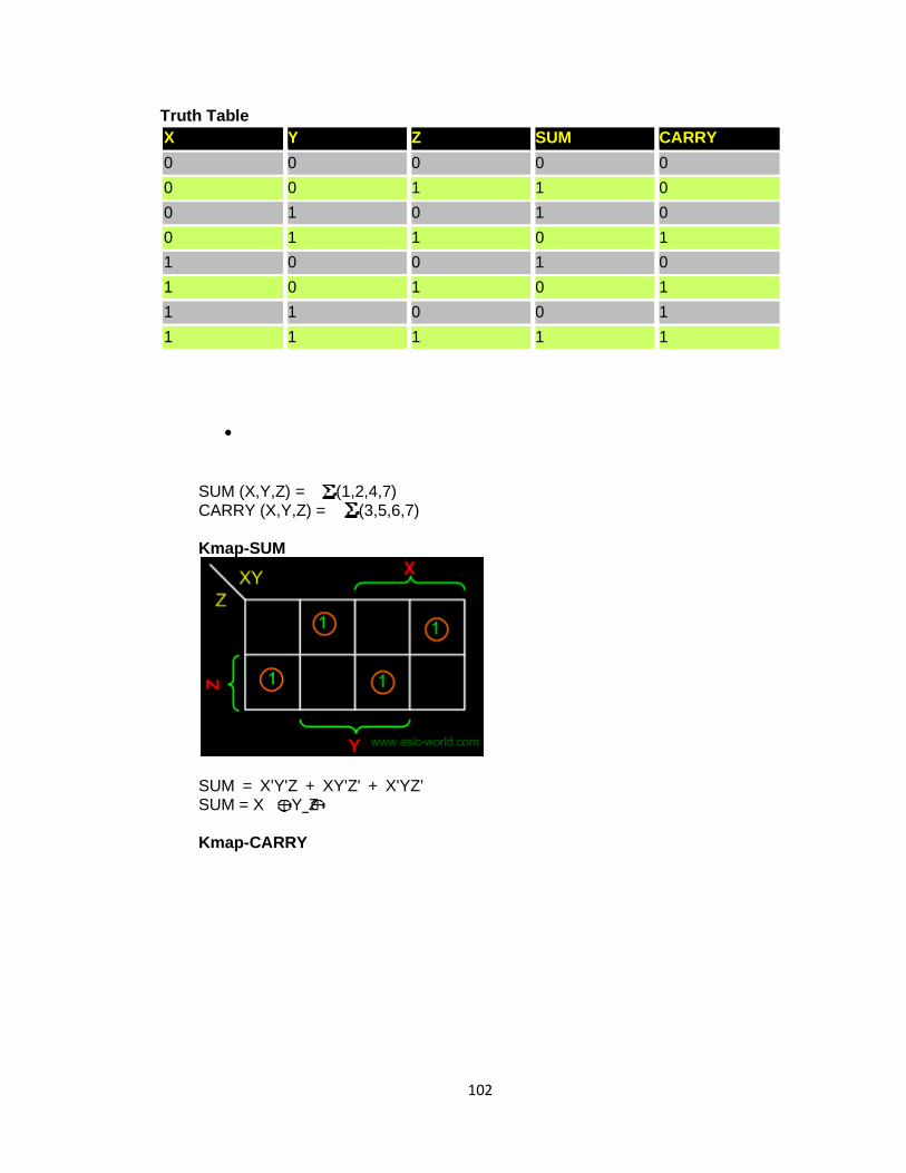
102
102
Truth Table
X Y Z SUM CARRY
0 0 0 0 0
0 0 1 1 0
0 1 0 1 0
0 1 1 0 1
1 0 0 1 0
1 0 1 0 1
1 1 0 0 1
1 1 1 1 1
•
SUM (X,Y,Z) = (1,2,4,7) CARRY (X,Y,Z) = (3,5,6,7)
Kmap-SUM
SUM = X'Y'Z + XY'Z' + X'YZ' SUM = X Y Z
Kmap-CARRY
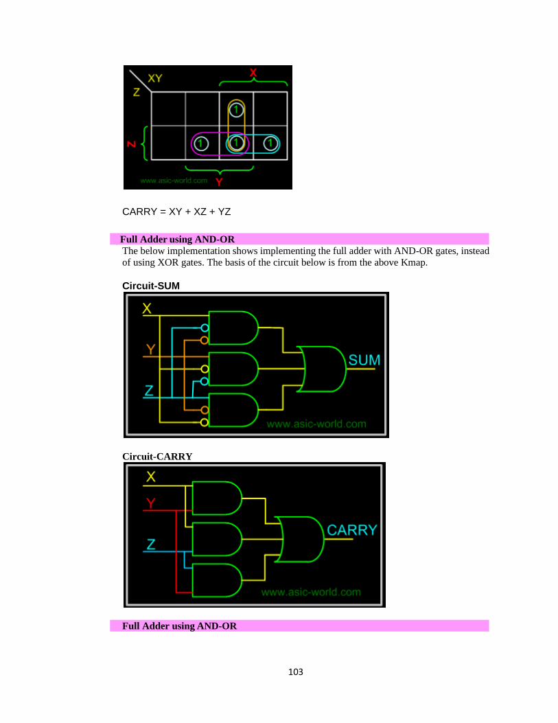
103
103
CARRY = XY + XZ + YZ
Full Adder using AND-OR
The below implementation shows implementing the full adder with AND-OR gates, instead
of using XOR gates. The basis of the circuit below is from the above Kmap.
Circuit-SUM
Circuit-CARRY
Full Adder using AND-OR
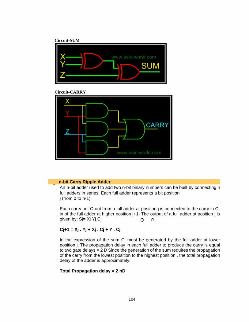
104
104
Circuit-SUM
Circuit-CARRY
n-bit Carry Ripple Adder
An n-bit adder used to add two n-bit binary numbers can be built by connecting n
full adders in series. Each full adder represents a bit position
j (from 0 to n-1).
Each carry out C-out from a full adder at position j is connected to the carry in C-in of the full adder at higher position j+1. The output of a full adder at position j is given by: Sj= Xj Yj Cj
Cj+1 = Xj . Yj + Xj . Cj + Y . Cj
In the expression of the sum Cj must be generated by the full adder at lower position j. The propagation delay in each full adder to produce the carry is equal to two gate delays = 2 D Since the generation of the sum requires the propagation of the carry from the lowest position to the highest position , the total propagation delay of the adder is approximately:
Total Propagation delay = 2 nD
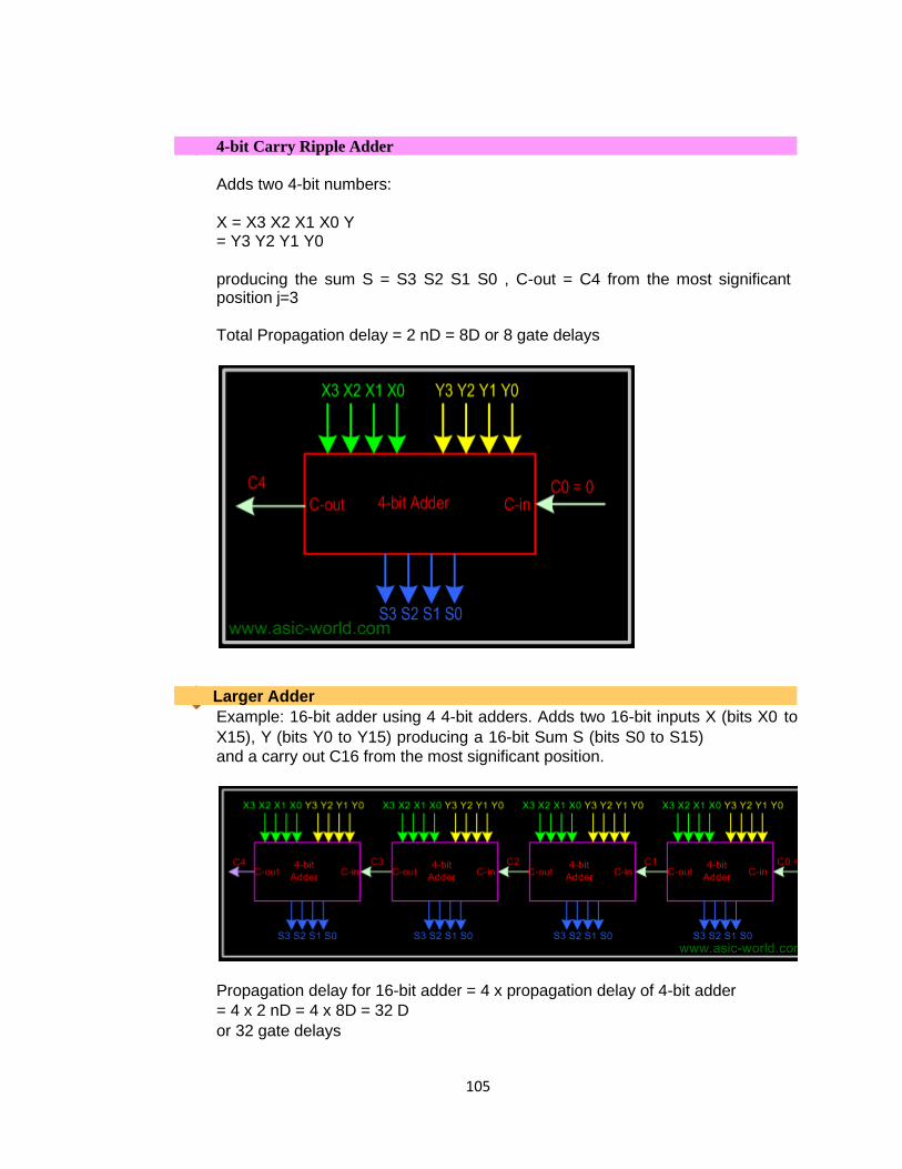
105
105
4-bit Carry Ripple Adder
Adds two 4-bit numbers:
X = X3 X2 X1 X0 Y = Y3 Y2 Y1 Y0
producing the sum S = S3 S2 S1 S0 , C-out = C4 from the most significant position j=3
Total Propagation delay = 2 nD = 8D or 8 gate delays
Larger Adder
Example: 16-bit adder using 4 4-bit adders. Adds two 16-bit inputs X (bits X0 to
X15), Y (bits Y0 to Y15) producing a 16-bit Sum S (bits S0 to S15)
and a carry out C16 from the most significant position.
Propagation delay for 16-bit adder = 4 x propagation delay of 4-bit adder
= 4 x 2 nD = 4 x 8D = 32 D
or 32 gate delays
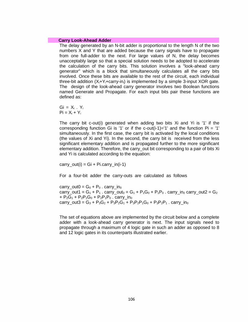
106
106
Carry Look-Ahead Adder The delay generated by an N-bit adder is proportional to the length N of the two numbers X and Y that are added because the carry signals have to propagate from one full-adder to the next. For large values of N, the delay becomes unacceptably large so that a special solution needs to be adopted to accelerate the calculation of the carry bits. This solution involves a "look-ahead carry generator" which is a block that simultaneously calculates all the carry bits involved. Once these bits are available to the rest of the circuit, each individual three-bit addition (Xi+Yi+carry-ini) is implemented by a simple 3-input XOR gate. The design of the look-ahead carry generator involves two Boolean functions named Generate and Propagate. For each input bits pair these functions are defined as:
Gi = Xi . Yi Pi = Xi + Yi
The carry bit c-out(i) generated when adding two bits Xi and Yi is '1' if the corresponding function Gi is '1' or if the c-out(i-1)='1' and the function Pi = '1' simultaneously. In the first case, the carry bit is activated by the local conditions (the values of Xi and Yi). In the second, the carry bit is received from the less significant elementary addition and is propagated further to the more significant elementary addition. Therefore, the carry_out bit corresponding to a pair of bits Xi and Yi is calculated according to the equation:
carry_out(i) = Gi + Pi.carry_in(i-1)
For a four-bit adder the carry-outs are calculated as follows
carry_out0 = G0 + P0 . carry_in0 carry_out1 = G1 + P1 . carry_out0 = G1 + P1G0 + P1P0 . carry_in0 carry_out2 = G2 + P2G1 + P2P1G0 + P2P1P0 . carry_in0 carry_out3 = G3 + P3G2 + P3P2G1 + P3P2P1G0 + P3P2P1 . carry_in0
The set of equations above are implemented by the circuit below and a complete adder with a look-ahead carry generator is next. The input signals need to propagate through a maximum of 4 logic gate in such an adder as opposed to 8 and 12 logic gates in its counterparts illustrated earlier.

107
107
Sums can be calculated from the following equations, where carry_out is taken from the carry calculated in the above circuit.
sum_out0 = X 0 Y0 carry_out0 sum_out1 = X 1 Y1 carry_out1 sum_out2 = X 2 Y2 carry_out2 sum_out3 = X 3 Y3 carry_out3
BCD Adder
BCD addition is the same as binary addition with a bit of variation: whenever a
sum is greater than 1001, it is not a valid BCD number, so we
add 0110 to it, to do the correction. This will produce a carry, which is
added to the next BCD position.
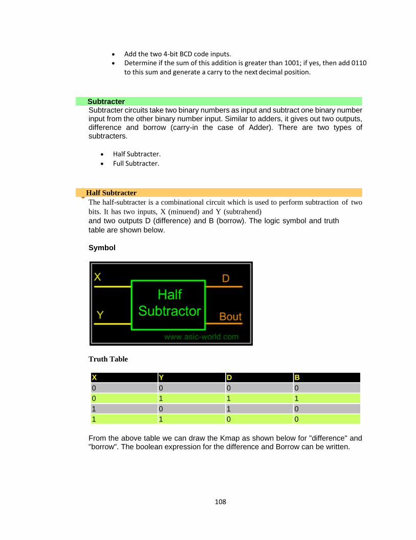
108
108
• Add the two 4-bit BCD code inputs. • Determine if the sum of this addition is greater than 1001; if yes, then add 0110
to this sum and generate a carry to the next decimal position.
Subtracter Subtracter circuits take two binary numbers as input and subtract one binary number input from the other binary number input. Similar to adders, it gives out two outputs, difference and borrow (carry-in the case of Adder). There are two types of subtracters.
• Half Subtracter. • Full Subtracter.
Half Subtracter
The half-subtracter is a combinational circuit which is used to perform subtraction of two
bits. It has two inputs, X (minuend) and Y (subtrahend)
and two outputs D (difference) and B (borrow). The logic symbol and truth
table are shown below.
Symbol
Truth Table
X Y D B
0 0 0 0
0 1 1 1
1 0 1 0
1 1 0 0
From the above table we can draw the Kmap as shown below for "difference" and "borrow". The boolean expression for the difference and Borrow can be written.
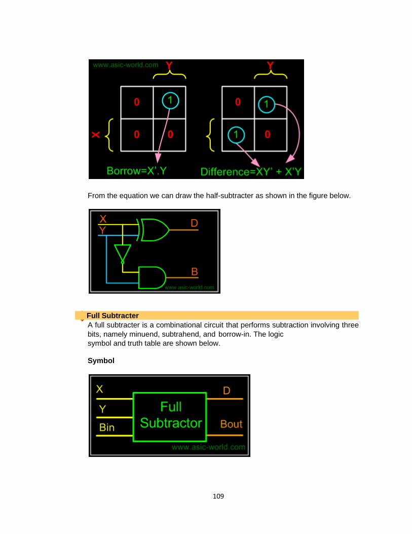
109
109
From the equation we can draw the half-subtracter as shown in the figure below.
Full Subtracter
A full subtracter is a combinational circuit that performs subtraction involving three
bits, namely minuend, subtrahend, and borrow-in. The logic
symbol and truth table are shown below.
Symbol
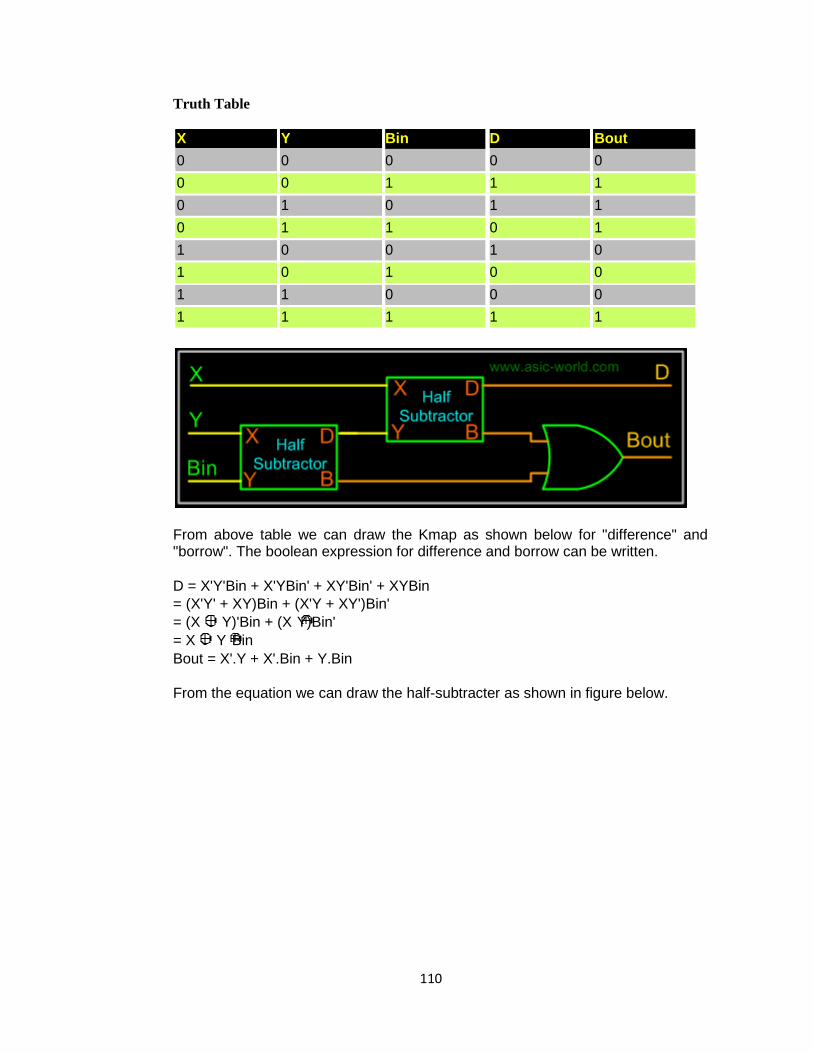
110
110
Truth Table
X Y Bin D Bout
0 0 0 0 0
0 0 1 1 1
0 1 0 1 1
0 1 1 0 1
1 0 0 1 0
1 0 1 0 0
1 1 0 0 0
1 1 1 1 1
From above table we can draw the Kmap as shown below for "difference" and "borrow". The boolean expression for difference and borrow can be written.
D = X'Y'Bin + X'YBin' + XY'Bin' + XYBin
= (X'Y' + XY)Bin + (X'Y + XY')Bin'
= (X Y)'Bin + (X Y)Bin'
= X Y Bin
Bout = X'.Y + X'.Bin + Y.Bin
From the equation we can draw the half-subtracter as shown in figure below.
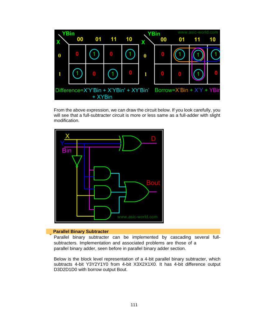
111
111
From the above expression, we can draw the circuit below. If you look carefully, you will see that a full-subtracter circuit is more or less same as a full-adder with slight modification.
Parallel Binary Subtracter
Parallel binary subtracter can be implemented by cascading several full-
subtracters. Implementation and associated problems are those of a
parallel binary adder, seen before in parallel binary adder section.
Below is the block level representation of a 4-bit parallel binary subtracter, which subtracts 4-bit Y3Y2Y1Y0 from 4-bit X3X2X1X0. It has 4-bit difference output D3D2D1D0 with borrow output Bout.
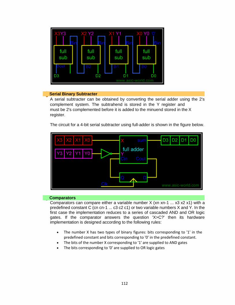
112
112
Serial Binary Subtracter
A serial subtracter can be obtained by converting the serial adder using the 2's
complement system. The subtrahend is stored in the Y register and
must be 2's complemented before it is added to the minuend stored in the X
register.
The circuit for a 4-bit serial subtracter using full-adder is shown in the figure below.
Comparators
Comparators can compare either a variable number X (xn xn-1 ... x3 x2 x1) with a predefined constant C (cn cn-1 ... c3 c2 c1) or two variable numbers X and Y. In the first case the implementation reduces to a series of cascaded AND and OR logic gates. If the comparator answers the question 'X>C?' then its hardware implementation is designed according to the following rules:
• The number X has two types of binary figures: bits corresponding to '1' in the
predefined constant and bits corresponding to '0' in the predefined constant. • The bits of the number X corresponding to '1' are supplied to AND gates • The bits corresponding to '0' are supplied to OR logic gates
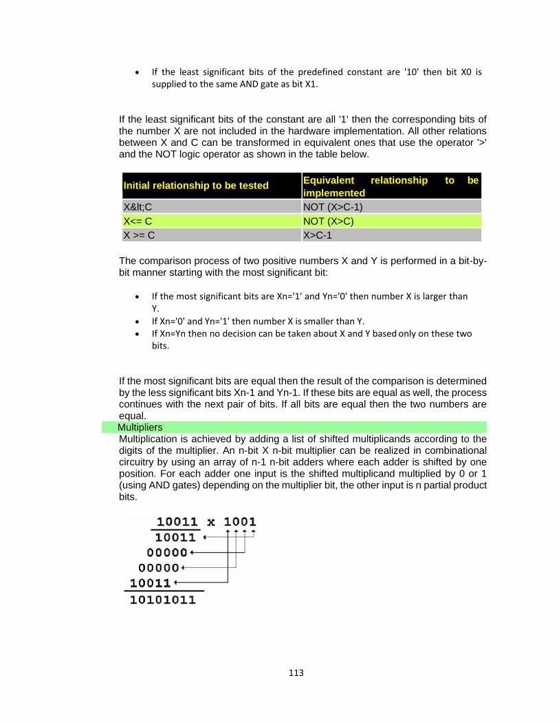
113
113
• If the least significant bits of the predefined constant are '10' then bit X0 is supplied to the same AND gate as bit X1.
If the least significant bits of the constant are all '1' then the corresponding bits of the number X are not included in the hardware implementation. All other relations between X and C can be transformed in equivalent ones that use the operator '>' and the NOT logic operator as shown in the table below.
Initial relationship to be tested Equivalent relationship to be
implemented
X<C NOT (X>C-1)
X<= C NOT (X>C)
X >= C X>C-1
The comparison process of two positive numbers X and Y is performed in a bit-by-bit manner starting with the most significant bit:
• If the most significant bits are Xn='1' and Yn='0' then number X is larger than
Y.
• If Xn='0' and Yn='1' then number X is smaller than Y. • If Xn=Yn then no decision can be taken about X and Y based only on these two
bits.
If the most significant bits are equal then the result of the comparison is determined by the less significant bits Xn-1 and Yn-1. If these bits are equal as well, the process continues with the next pair of bits. If all bits are equal then the two numbers are equal.
Multipliers Multiplication is achieved by adding a list of shifted multiplicands according to the digits of the multiplier. An n-bit X n-bit multiplier can be realized in combinational circuitry by using an array of n-1 n-bit adders where each adder is shifted by one position. For each adder one input is the shifted multiplicand multiplied by 0 or 1 (using AND gates) depending on the multiplier bit, the other input is n partial product bits.
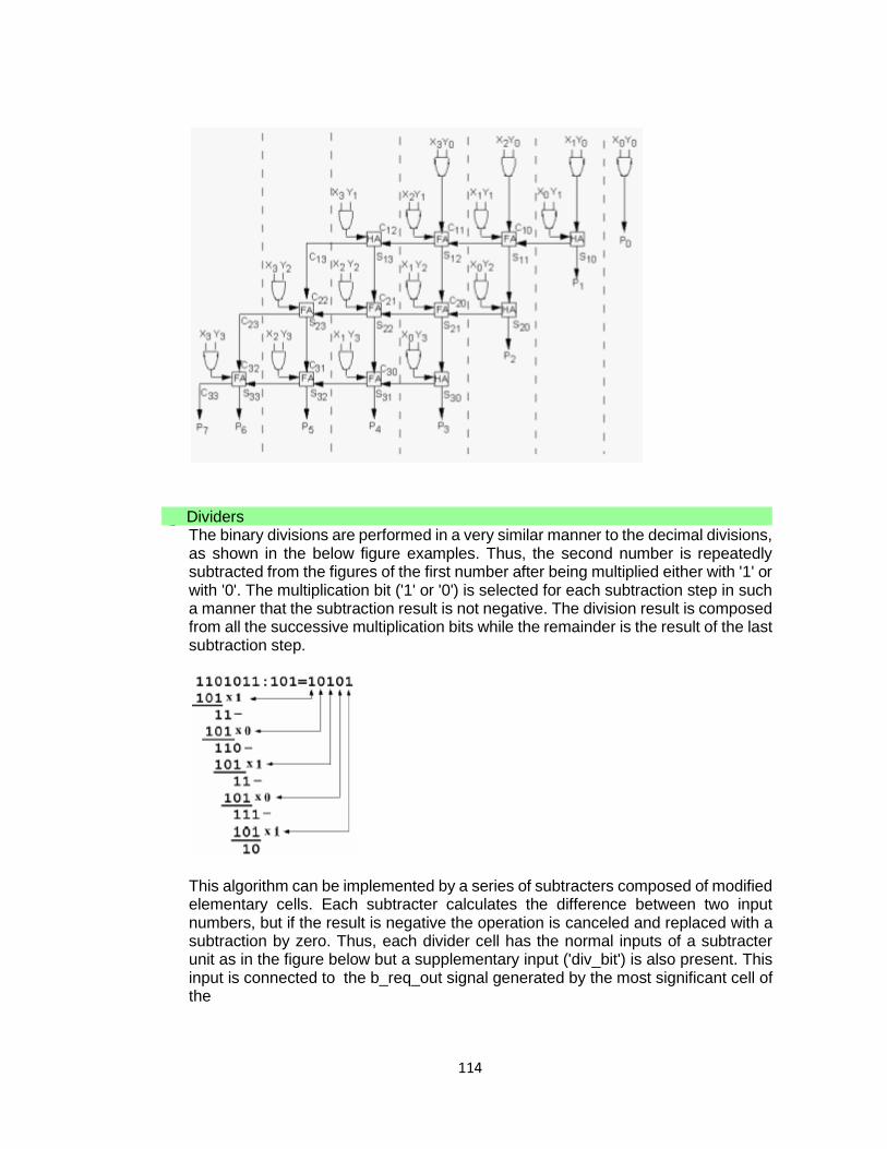
114
114
Dividers The binary divisions are performed in a very similar manner to the decimal divisions, as shown in the below figure examples. Thus, the second number is repeatedly subtracted from the figures of the first number after being multiplied either with '1' or with '0'. The multiplication bit ('1' or '0') is selected for each subtraction step in such a manner that the subtraction result is not negative. The division result is composed from all the successive multiplication bits while the remainder is the result of the last subtraction step.
This algorithm can be implemented by a series of subtracters composed of modified elementary cells. Each subtracter calculates the difference between two input numbers, but if the result is negative the operation is canceled and replaced with a subtraction by zero. Thus, each divider cell has the normal inputs of a subtracter unit as in the figure below but a supplementary input ('div_bit') is also present. This input is connected to the b_req_out signal generated by the most significant cell of the
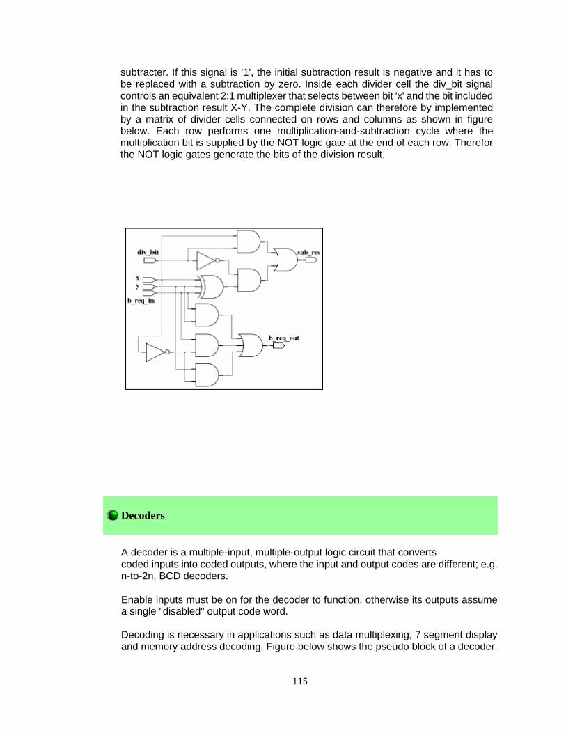
115
115
subtracter. If this signal is '1', the initial subtraction result is negative and it has to be replaced with a subtraction by zero. Inside each divider cell the div_bit signal controls an equivalent 2:1 multiplexer that selects between bit 'x' and the bit included in the subtraction result X-Y. The complete division can therefore by implemented by a matrix of divider cells connected on rows and columns as shown in figure below. Each row performs one multiplication-and-subtraction cycle where the multiplication bit is supplied by the NOT logic gate at the end of each row. Therefor the NOT logic gates generate the bits of the division result.
A decoder is a multiple-input, multiple-output logic circuit that converts coded inputs into coded outputs, where the input and output codes are different; e.g. n-to-2n, BCD decoders.
Enable inputs must be on for the decoder to function, otherwise its outputs assume a single "disabled" output code word.
Decoding is necessary in applications such as data multiplexing, 7 segment display and memory address decoding. Figure below shows the pseudo block of a decoder.
Decoders

116
116
Basic Binary Decoder
And AND gate can be used as the basic decoding element, because its output is
HIGH only when all its inputs are HIGH. For example, if the input
binary number is 0110, then, to make all the inputs to the AND gate HIGH,
the two outer bits must be inverted using two inverters as shown in figure below.
A binary decoder has n inputs and 2n outputs. Only one output is active at any one time, corresponding to the input value. Figure below shows a representation of Binary n-to-2n decoder
Binary n-to-2n Decoders

117
117
Example - 2-to-4 Binary Decoder
A 2 to 4 decoder consists of two inputs and four outputs, truth table and symbols of which is
shown below.
Truth Table
X Y F0 F1 F2 F3
0 0 1 0 0 0
0 1 0 1 0 0
1 0 0 0 1 0
1 1 0 0 0 1
Symbol
To minimize the above truth table we may use kmap, but doing that you will realize that it is a waste of time. One can directly write down the function for each of the outputs. Thus we can draw the circuit as shown in figure below.
Note: Each output is a 2-variable minterm (X'Y', X'Y, XY', XY)
Circuit
Example - 3-to-8 Binary Decoder
A 3 to 8 decoder consists of three inputs and eight outputs, truth table and symbols of which is shown below.
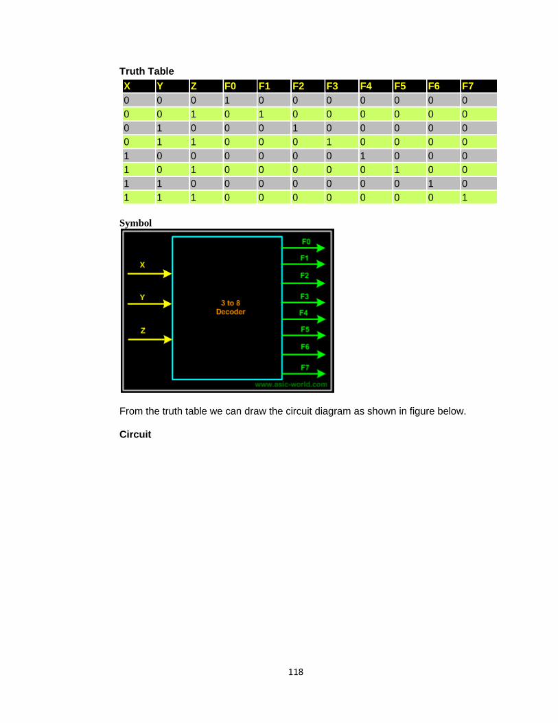
118
118
Truth Table
X Y Z F0 F1 F2 F3 F4 F5 F6 F7
0 0 0 1 0 0 0 0 0 0 0
0 0 1 0 1 0 0 0 0 0 0
0 1 0 0 0 1 0 0 0 0 0
0 1 1 0 0 0 1 0 0 0 0
1 0 0 0 0 0 0 1 0 0 0
1 0 1 0 0 0 0 0 1 0 0
1 1 0 0 0 0 0 0 0 1 0
1 1 1 0 0 0 0 0 0 0 1
Symbol
From the truth table we can draw the circuit diagram as shown in figure below.
Circuit
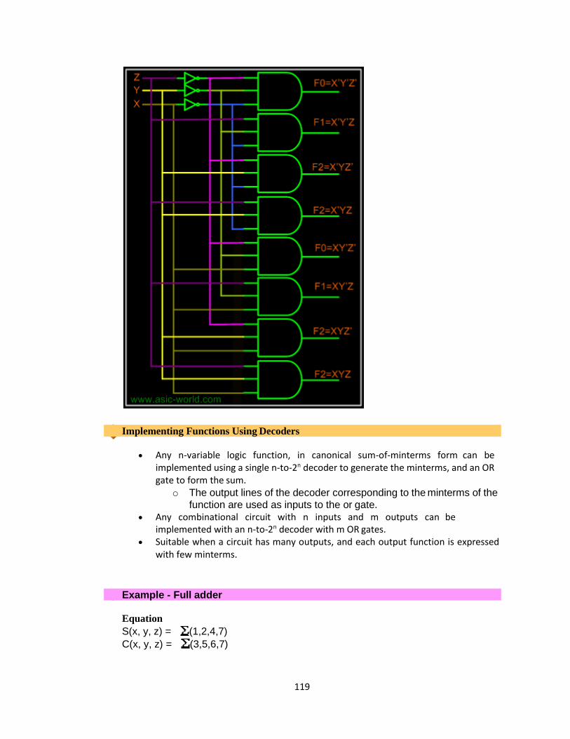
119
119
Implementing Functions Using Decoders
• Any n-variable logic function, in canonical sum-of-minterms form can be
implemented using a single n-to-2n decoder to generate the minterms, and an OR gate to form the sum.
o The output lines of the decoder corresponding to the minterms of the
function are used as inputs to the or gate.
• Any combinational circuit with n inputs and m outputs can be implemented with an n-to-2n decoder with m OR gates.
• Suitable when a circuit has many outputs, and each output function is expressed with few minterms.
Example - Full adder
Equation
S(x, y, z) = (1,2,4,7)
C(x, y, z) = (3,5,6,7)
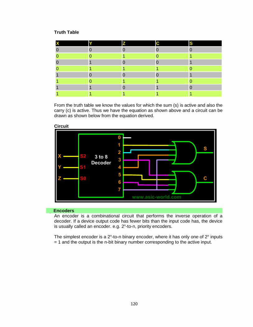
120
120
Truth Table
X Y Z C S
0 0 0 0 0
0 0 1 0 1
0 1 0 0 1
0 1 1 1 0
1 0 0 0 1
1 0 1 1 0
1 1 0 1 0
1 1 1 1 1
From the truth table we know the values for which the sum (s) is active and also the carry (c) is active. Thus we have the equation as shown above and a circuit can be drawn as shown below from the equation derived.
Circuit
Encoders An encoder is a combinational circuit that performs the inverse operation of a decoder. If a device output code has fewer bits than the input code has, the device is usually called an encoder. e.g. 2n-to-n, priority encoders.
The simplest encoder is a 2n-to-n binary encoder, where it has only one of 2n inputs = 1 and the output is the n-bit binary number corresponding to the active input.
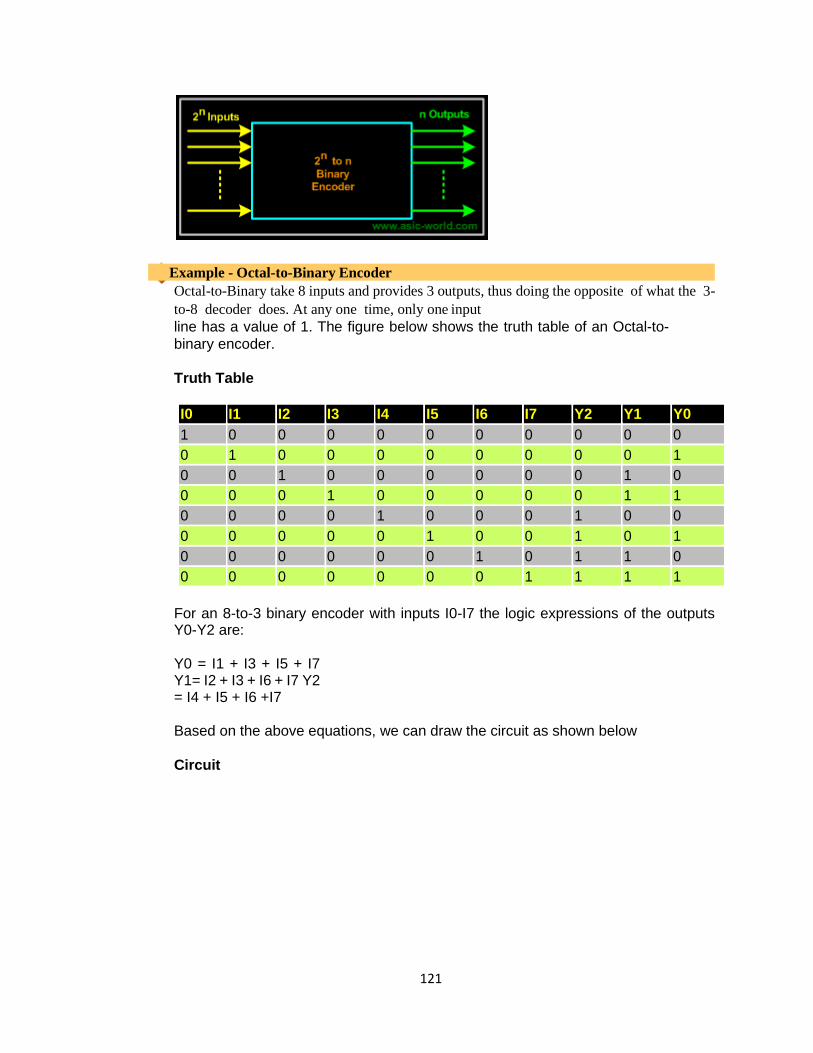
121
121
Example - Octal-to-Binary Encoder
Octal-to-Binary take 8 inputs and provides 3 outputs, thus doing the opposite of what the 3-
to-8 decoder does. At any one time, only one input
line has a value of 1. The figure below shows the truth table of an Octal-to-
binary encoder.
Truth Table
I0 I1 I2 I3 I4 I5 I6 I7 Y2 Y1 Y0
1 0 0 0 0 0 0 0 0 0 0
0 1 0 0 0 0 0 0 0 0 1
0 0 1 0 0 0 0 0 0 1 0
0 0 0 1 0 0 0 0 0 1 1
0 0 0 0 1 0 0 0 1 0 0
0 0 0 0 0 1 0 0 1 0 1
0 0 0 0 0 0 1 0 1 1 0
0 0 0 0 0 0 0 1 1 1 1
For an 8-to-3 binary encoder with inputs I0-I7 the logic expressions of the outputs Y0-Y2 are:
Y0 = I1 + I3 + I5 + I7 Y1= I2 + I3 + I6 + I7 Y2 = I4 + I5 + I6 +I7
Based on the above equations, we can draw the circuit as shown below
Circuit
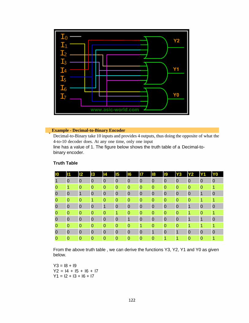
122
122
Example - Decimal-to-Binary Encoder
Decimal-to-Binary take 10 inputs and provides 4 outputs, thus doing the opposite of what the
4-to-10 decoder does. At any one time, only one input
line has a value of 1. The figure below shows the truth table of a Decimal-to-
binary encoder.
Truth Table
I0 I1 I2 I3 I4 I5 I6 I7 I8 I9 Y3 Y2 Y1 Y0
1 0 0 0 0 0 0 0 0 0 0 0 0 0
0 1 0 0 0 0 0 0 0 0 0 0 0 1
0 0 1 0 0 0 0 0 0 0 0 0 1 0
0 0 0 1 0 0 0 0 0 0 0 0 1 1
0 0 0 0 1 0 0 0 0 0 0 1 0 0
0 0 0 0 0 1 0 0 0 0 0 1 0 1
0 0 0 0 0 0 1 0 0 0 0 1 1 0
0 0 0 0 0 0 0 1 0 0 0 1 1 1
0 0 0 0 0 0 0 0 1 0 1 0 0 0
0 0 0 0 0 0 0 0 0 1 1 0 0 1
From the above truth table , we can derive the functions Y3, Y2, Y1 and Y0 as given below.
Y3 = I8 + I9
Y2 = I4 + I5 + I6 + I7 Y1 = I2 + I3 + I6 + I7
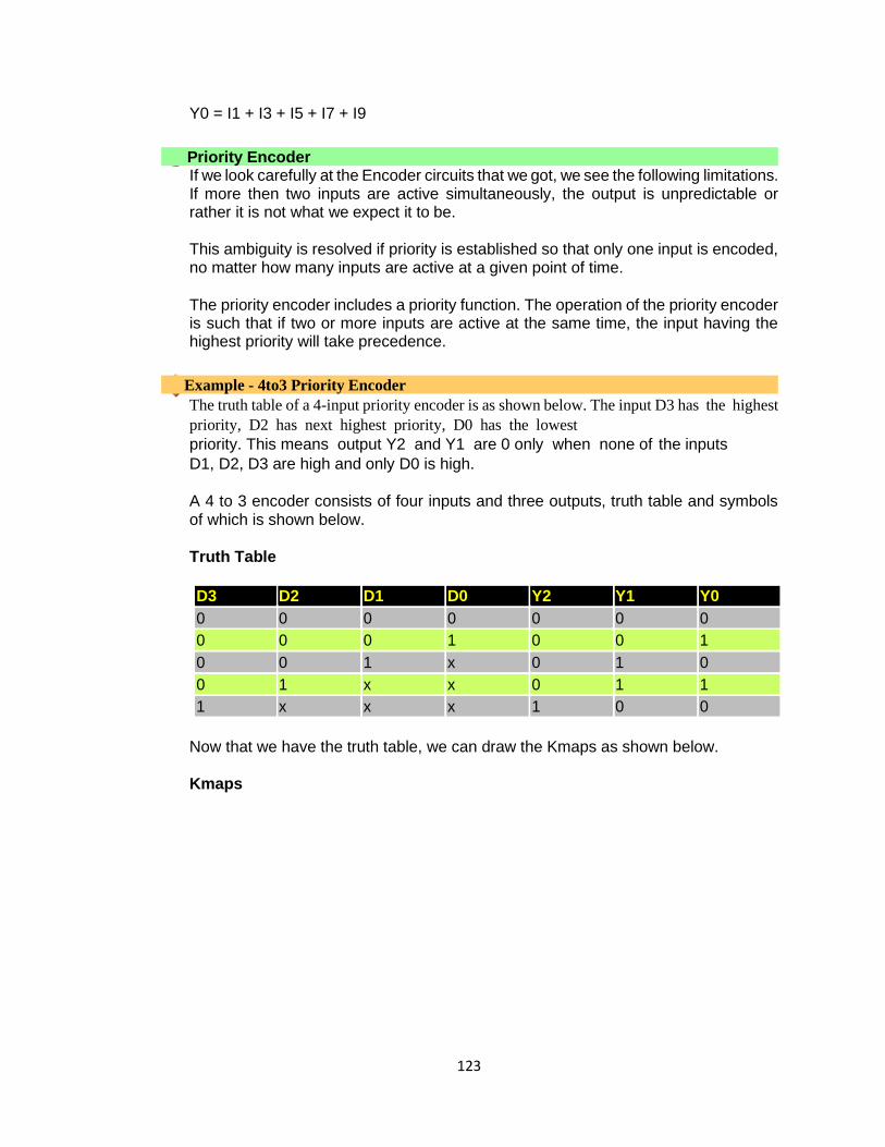
123
123
Y0 = I1 + I3 + I5 + I7 + I9
Priority Encoder If we look carefully at the Encoder circuits that we got, we see the following limitations. If more then two inputs are active simultaneously, the output is unpredictable or rather it is not what we expect it to be.
This ambiguity is resolved if priority is established so that only one input is encoded, no matter how many inputs are active at a given point of time.
The priority encoder includes a priority function. The operation of the priority encoder is such that if two or more inputs are active at the same time, the input having the highest priority will take precedence.
Example - 4to3 Priority Encoder
The truth table of a 4-input priority encoder is as shown below. The input D3 has the highest
priority, D2 has next highest priority, D0 has the lowest
priority. This means output Y2 and Y1 are 0 only when none of the inputs
D1, D2, D3 are high and only D0 is high.
A 4 to 3 encoder consists of four inputs and three outputs, truth table and symbols of which is shown below.
Truth Table
D3 D2 D1 D0 Y2 Y1 Y0
0 0 0 0 0 0 0
0 0 0 1 0 0 1
0 0 1 x 0 1 0
0 1 x x 0 1 1
1 x x x 1 0 0
Now that we have the truth table, we can draw the Kmaps as shown below.
Kmaps
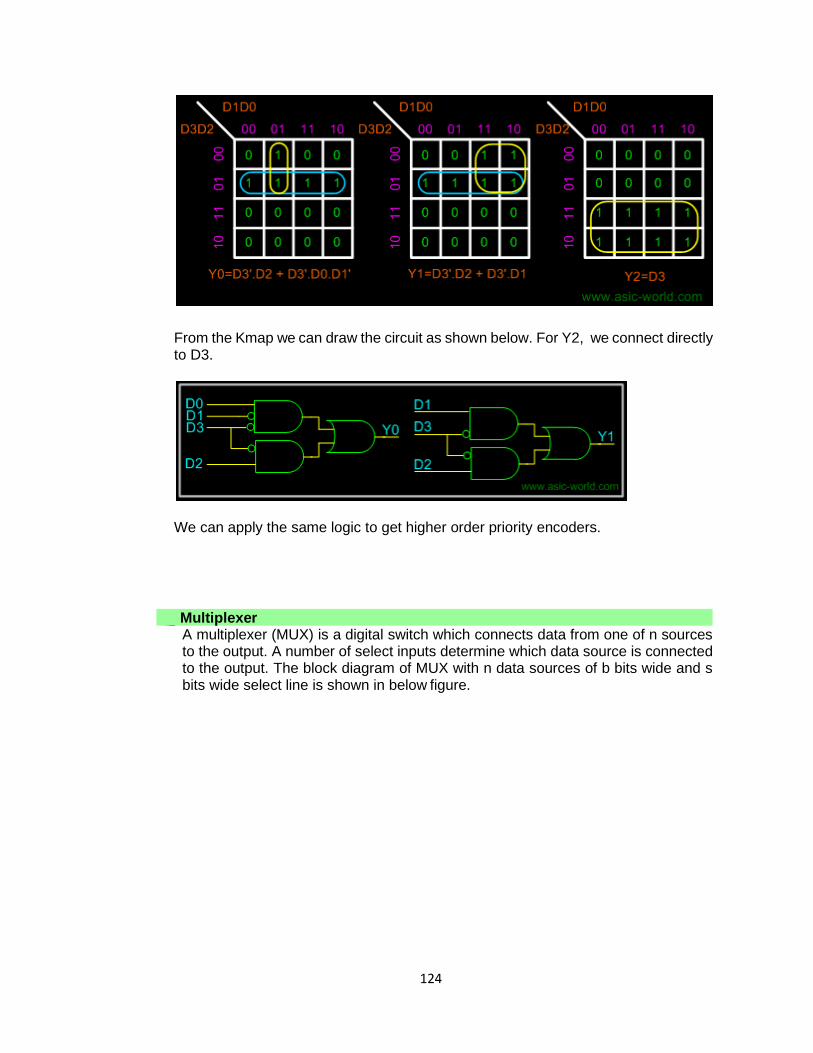
124
124
From the Kmap we can draw the circuit as shown below. For Y2, we connect directly to D3.
We can apply the same logic to get higher order priority encoders.
Multiplexer A multiplexer (MUX) is a digital switch which connects data from one of n sources to the output. A number of select inputs determine which data source is connected to the output. The block diagram of MUX with n data sources of b bits wide and s bits wide select line is shown in below figure.
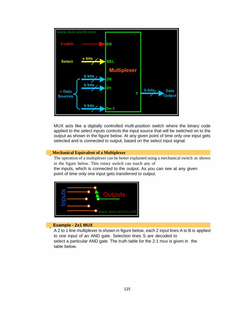
125
125
MUX acts like a digitally controlled multi-position switch where the binary code applied to the select inputs controls the input source that will be switched on to the output as shown in the figure below. At any given point of time only one input gets selected and is connected to output, based on the select input signal.
Mechanical Equivalent of a Multiplexer
The operation of a multiplexer can be better explained using a mechanical switch as shown
in the figure below. This rotary switch can touch any of
the inputs, which is connected to the output. As you can see at any given
point of time only one input gets transferred to output.
Example - 2x1 MUX
A 2 to 1 line multiplexer is shown in figure below, each 2 input lines A to B is applied
to one input of an AND gate. Selection lines S are decoded to
select a particular AND gate. The truth table for the 2:1 mux is given in the
table below.
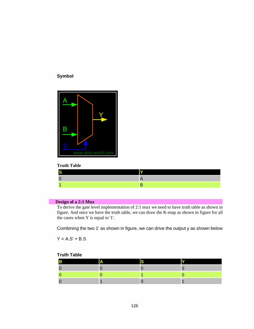
126
126
Symbol
Truth Table
S Y
0 A
1 B
Design of a 2:1 Mux
To derive the gate level implementation of 2:1 mux we need to have truth table as shown in
figure. And once we have the truth table, we can draw the K-map as shown in figure for all
the cases when Y is equal to '1'.
Combining the two 1' as shown in figure, we can drive the output y as shown below
Y = A.S' + B.S
Truth Table
B A S Y
0 0 0 0
0 0 1 0
0 1 0 1
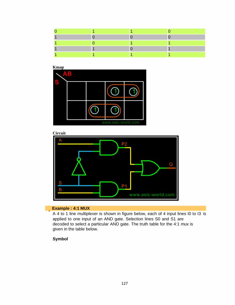
127
127
0 1 1 0
1 0 0 0
1 0 1 1
1 1 0 1
1 1 1 1
Kmap
Circuit
Example : 4:1 MUX
A 4 to 1 line multiplexer is shown in figure below, each of 4 input lines I0 to I3 is
applied to one input of an AND gate. Selection lines S0 and S1 are
decoded to select a particular AND gate. The truth table for the 4:1 mux is
given in the table below.
Symbol
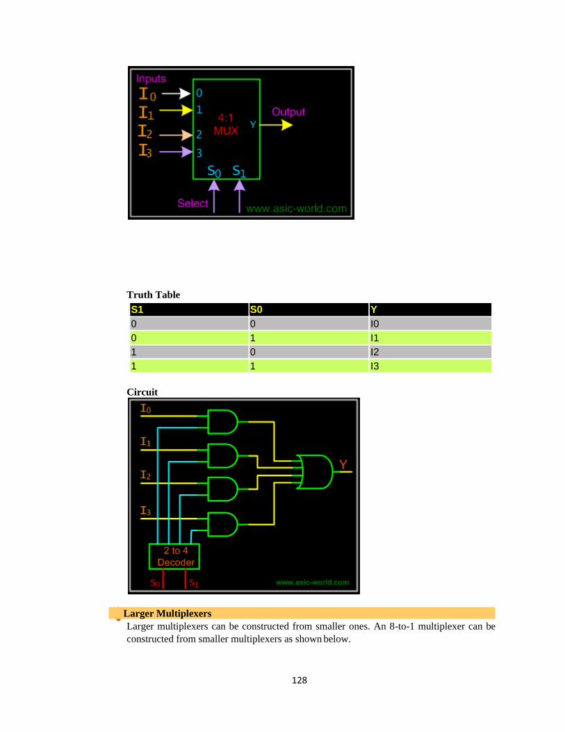
128
128
Truth Table
S1 S0 Y
0 0 I0
0 1 I1
1 0 I2
1 1 I3
Circuit
Larger Multiplexers
Larger multiplexers can be constructed from smaller ones. An 8-to-1 multiplexer can be
constructed from smaller multiplexers as shown below.
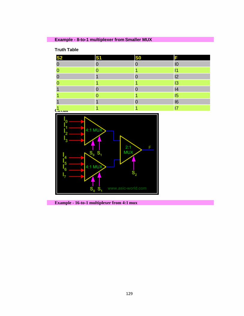
129
129
Example - 8-to-1 multiplexer from Smaller MUX
Truth Table
Circuit
Example - 16-to-1 multiplexer from 4:1 mux
S2 S1 S0 F
0 0 0 I0
0 0 1 I1
0 1 0 I2
0 1 1 I3
1 0 0 I4
1 0 1 I5
1 1 0 I6
1 1 1 I7

130
130
De-multiplexers
They are digital switches which connect data from one input source to one of n outputs.
Usually implemented by using n-to-2n binary decoders where the decoder enable line is used for data input of the de-multiplexer.
The figure below shows a de-multiplexer block diagram which has got s- bits-wide select input, one b-bits-wide data input and n b-bits-wide outputs.
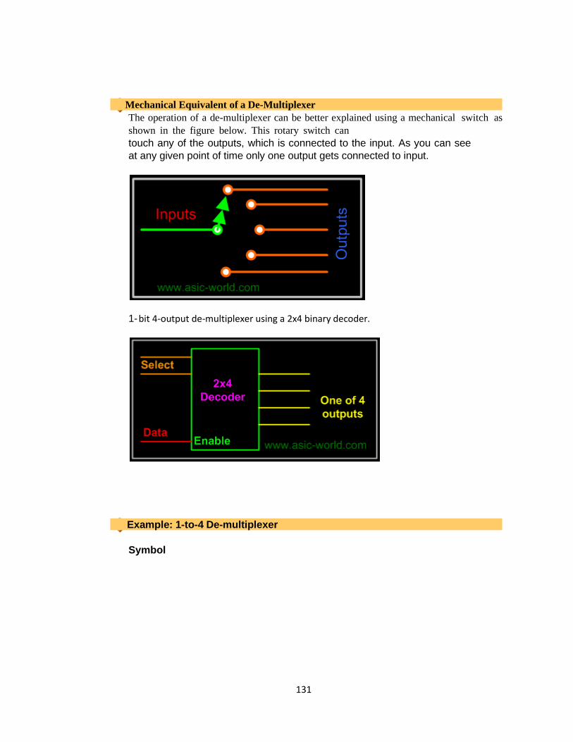
131
131
Mechanical Equivalent of a De-Multiplexer
The operation of a de-multiplexer can be better explained using a mechanical switch as
shown in the figure below. This rotary switch can
touch any of the outputs, which is connected to the input. As you can see
at any given point of time only one output gets connected to input.
1- bit 4-output de-multiplexer using a 2x4 binary decoder.
Example: 1-to-4 De-multiplexer
Symbol

132
132
Truth Table
S1 S0 F0 F1 F2 F3
0 0 D 0 0 0
0 1 0 D 0 0
1 0 0 0 D 0
1 1 0 0 0 D
Boolean Function Implementation Earlier we had seen that it is possible to implement Boolean functions using decoders. In the same way it is also possible to implement Boolean functions using muxers and de-muxers.
Implementing Functions Multiplexers
Any n-variable logic function can be implemented using a smaller 2n-1-to-1 multiplexer and
a single inverter (e.g 4-to-1 mux to implement 3 variable
functions) as follows.
Express function in canonical sum-of-minterms form. Choose n-1 variables as inputs to mux select lines. Construct the truth table for the function, but grouping inputs by selection line values (i.e select lines as most significant inputs). Determine multiplexer input line i values by comparing the remaining input variable and the function F for the corresponding selection lines value i.
We have four possible mux input line i values:
• Connect to 0 if the function is 0 for both values of remaining variable. • Connect to 1 if the function is 1 for both values of remaining
133
133
variable.
ct to remaining variable if function is equal to the remaining variable.
• Connect to the inverted remaining variable if the function is equal to the remaining variable inverted.
Example: 3-variable Function Using 8-to-1 mux
Implement the function F(X,Y,Z) = S(1,3,5,6) using an 8-to-1 mux. Connect the input
variables X, Y, Z to mux select lines. Mux data input lines 1, 3, 5,
6 that correspond to the function minterms are connected to 1. The remaining mux data input lines 0, 2, 4, 7 are connected to 0.
Example: 3-variable Function Using 4-to-1 mux
Implement the function F(X,Y,Z) = S(0,1,3,6) using a single 4-to-1 mux and an inverter.
We choose the two most significant inputs X, Y as mux select lines.
Construct truth table.
Truth Table
Select i X Y Z F Mux Input i
0 0 0 0 1 1
0 0 0 1 1 1
1 0 1 0 0 Z
1 0 1 1 1 Z
2 1 0 0 0 0
2 1 0 1 0 0
3 1 1 0 1 Z'
3 1 1 1 0 Z'
134
134
Circuit
We determine multiplexer input line i values by comparing the remaining input variable Z and the function F for the corresponding selection lines value i
• when XY=00 the function F is 1 (for both Z=0, Z=1) thus mux input0
= 1
• when XY=01 the function F is Z thus mux input1 = Z • when XY=10 the function F is 0 (for both Z=0, Z=1) thus mux input2
= 0
• when XY=11 the function F is Z' thus mux input3 = Z'
Example: 2 to 4 Decoder using Demux
Mux-Demux Application Example
This enables sharing a single communication line among a number of devices. At any time,
only one source and one destination can use the communication line.
135
135

136
136
Assignment UNIT 4
Academic Year 2020-21
Course : B.Tech.
Semester/
Section
: III Sem A
Subject &
Subject Code
: Digital Electronics & 3CS3-04 Max. Marks : 20
Course Outcomes
CO4 Design various combinational and sequential circuits
Q.
No.
Questions Marks
1. Implement full adder using two half adders 2
2. Implement half adder and full adder using NAND gates only 2
3. Design serial adder/subractor using a single circuit. 2
4. Describe 16:1 MUX using truth table and logic diagram. 2
5. Design 16:1 MUX using 4:1 MUX. 2
6. Implement the given Boolean expression using 8:1 MUX: Y=∑m (1,2,4,5,7) 2
7. Implement the given Boolean expression using Type 1 method: Y=∑m
(0,2,3,4,5,8,9,10,12,13)
2
8. Design 4:1 MUX for the given Boolean expression: Y=∑m (0,2,3,4,6,7,9,10,12,15) 2
9. Design BCD to Excess-3 code converter. 2
10. Design octal to binary decoder. 2
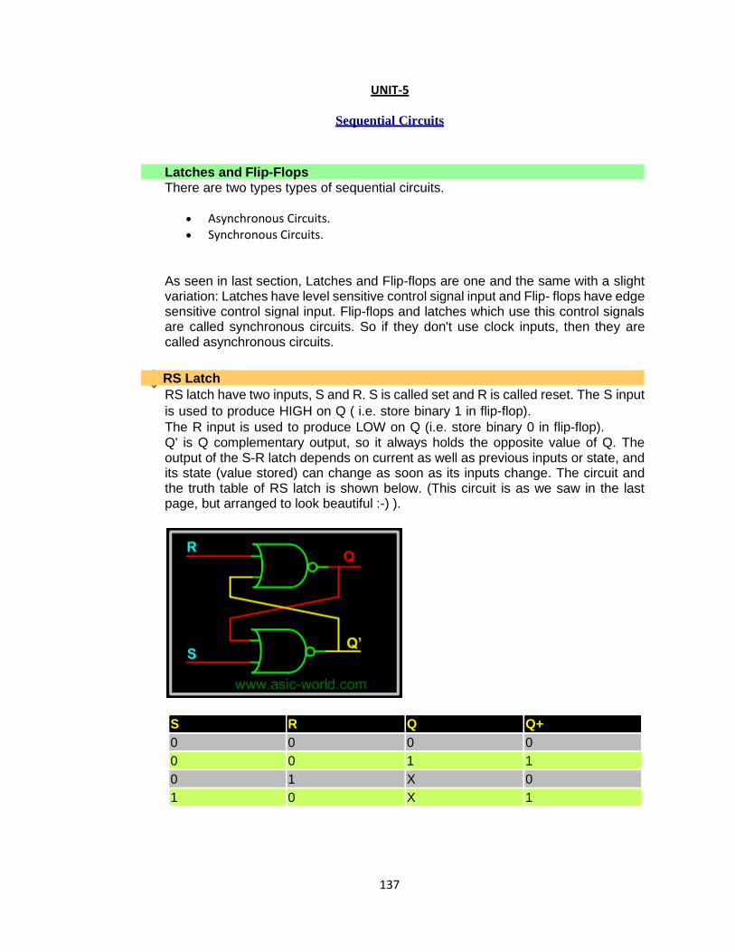
137
137
UNIT-5
Sequential Circuits
Latches and Flip-Flops There are two types types of sequential circuits.
• Asynchronous Circuits. • Synchronous Circuits.
As seen in last section, Latches and Flip-flops are one and the same with a slight variation: Latches have level sensitive control signal input and Flip- flops have edge sensitive control signal input. Flip-flops and latches which use this control signals are called synchronous circuits. So if they don't use clock inputs, then they are called asynchronous circuits.
RS Latch
RS latch have two inputs, S and R. S is called set and R is called reset. The S input
is used to produce HIGH on Q ( i.e. store binary 1 in flip-flop).
The R input is used to produce LOW on Q (i.e. store binary 0 in flip-flop). Q' is Q complementary output, so it always holds the opposite value of Q. The output of the S-R latch depends on current as well as previous inputs or state, and its state (value stored) can change as soon as its inputs change. The circuit and the truth table of RS latch is shown below. (This circuit is as we saw in the last page, but arranged to look beautiful :-) ).
S R Q Q+
0 0 0 0
0 0 1 1
0 1 X 0
1 0 X 1
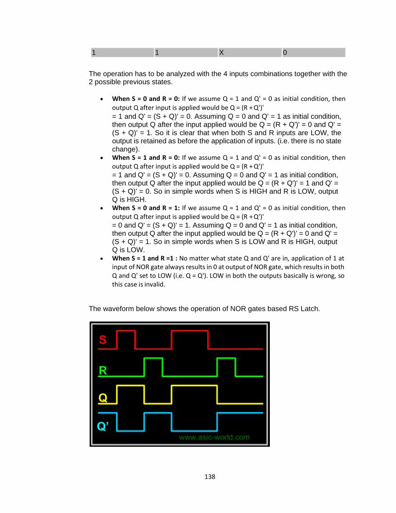
138
138
1 1 X 0
The operation has to be analyzed with the 4 inputs combinations together with the 2 possible previous states.
• When S = 0 and R = 0: If we assume Q = 1 and Q' = 0 as initial condition, then
output Q after input is applied would be Q = (R + Q')' = 1 and Q' = (S + Q)' = 0. Assuming Q = 0 and Q' = 1 as initial condition, then output Q after the input applied would be Q = (R + Q')' = 0 and Q' = (S + Q)' = 1. So it is clear that when both S and R inputs are LOW, the output is retained as before the application of inputs. (i.e. there is no state change).
• When S = 1 and R = 0: If we assume Q = 1 and Q' = 0 as initial condition, then output Q after input is applied would be Q = (R + Q')' = 1 and Q' = (S + Q)' = 0. Assuming Q = 0 and Q' = 1 as initial condition, then output Q after the input applied would be Q = (R + Q')' = 1 and Q' = (S + Q)' = 0. So in simple words when S is HIGH and R is LOW, output Q is HIGH.
• When S = 0 and R = 1: If we assume Q = 1 and Q' = 0 as initial condition, then output Q after input is applied would be Q = (R + Q')' = 0 and Q' = (S + Q)' = 1. Assuming Q = 0 and Q' = 1 as initial condition, then output Q after the input applied would be Q = (R + Q')' = 0 and Q' = (S + Q)' = 1. So in simple words when S is LOW and R is HIGH, output Q is LOW.
• When S = 1 and R =1 : No matter what state Q and Q' are in, application of 1 at input of NOR gate always results in 0 at output of NOR gate, which results in both Q and Q' set to LOW (i.e. Q = Q'). LOW in both the outputs basically is wrong, so this case is invalid.
The waveform below shows the operation of NOR gates based RS Latch.
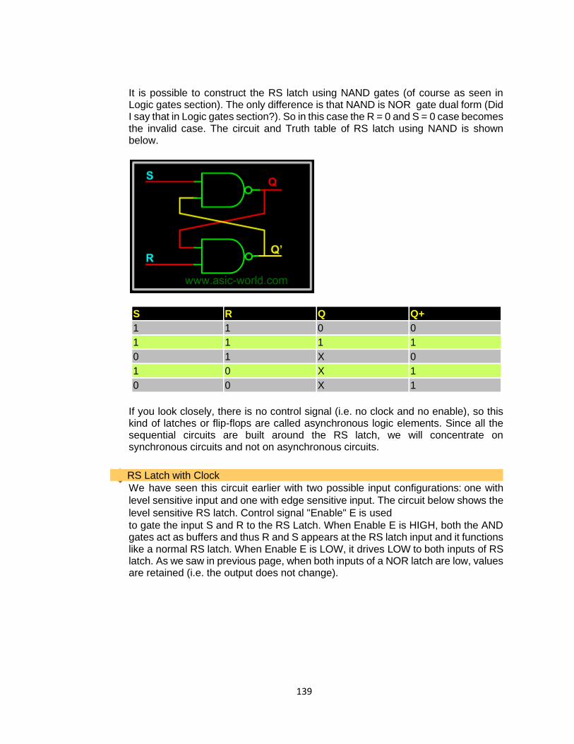
139
139
It is possible to construct the RS latch using NAND gates (of course as seen in Logic gates section). The only difference is that NAND is NOR gate dual form (Did I say that in Logic gates section?). So in this case the R = 0 and S = 0 case becomes the invalid case. The circuit and Truth table of RS latch using NAND is shown below.
S R Q Q+
1 1 0 0
1 1 1 1
0 1 X 0
1 0 X 1
0 0 X 1
If you look closely, there is no control signal (i.e. no clock and no enable), so this kind of latches or flip-flops are called asynchronous logic elements. Since all the sequential circuits are built around the RS latch, we will concentrate on synchronous circuits and not on asynchronous circuits.
RS Latch with Clock
We have seen this circuit earlier with two possible input configurations: one with
level sensitive input and one with edge sensitive input. The circuit below shows the
level sensitive RS latch. Control signal "Enable" E is used
to gate the input S and R to the RS Latch. When Enable E is HIGH, both the AND gates act as buffers and thus R and S appears at the RS latch input and it functions like a normal RS latch. When Enable E is LOW, it drives LOW to both inputs of RS latch. As we saw in previous page, when both inputs of a NOR latch are low, values are retained (i.e. the output does not change).
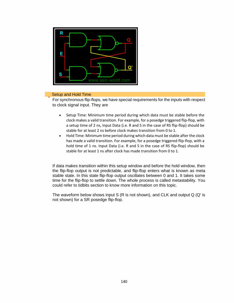
140
140
Setup and Hold Time
For synchronous flip-flops, we have special requirements for the inputs with respect
to clock signal input. They are
• Setup Time: Minimum time period during which data must be stable before the
clock makes a valid transition. For example, for a posedge triggered flip-flop, with a setup time of 2 ns, Input Data (i.e. R and S in the case of RS flip-flop) should be stable for at least 2 ns before clock makes transition from 0 to 1.
• Hold Time: Minimum time period during which data must be stable after the clock has made a valid transition. For example, for a posedge triggered flip-flop, with a hold time of 1 ns. Input Data (i.e. R and S in the case of RS flip-flop) should be stable for at least 1 ns after clock has made transition from 0 to 1.
If data makes transition within this setup window and before the hold window, then the flip-flop output is not predictable, and flip-flop enters what is known as meta stable state. In this state flip-flop output oscillates between 0 and 1. It takes some time for the flip-flop to settle down. The whole process is called metastability. You could refer to tidbits section to know more information on this topic.
The waveform below shows input S (R is not shown), and CLK and output Q (Q' is not shown) for a SR posedge flip-flop.
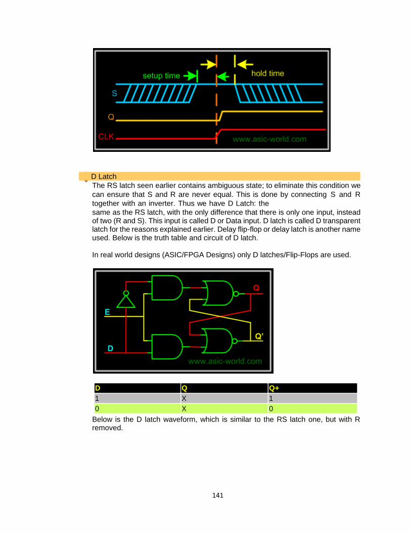
141
141
D Latch
The RS latch seen earlier contains ambiguous state; to eliminate this condition we
can ensure that S and R are never equal. This is done by connecting S and R
together with an inverter. Thus we have D Latch: the
same as the RS latch, with the only difference that there is only one input, instead of two (R and S). This input is called D or Data input. D latch is called D transparent latch for the reasons explained earlier. Delay flip-flop or delay latch is another name used. Below is the truth table and circuit of D latch.
In real world designs (ASIC/FPGA Designs) only D latches/Flip-Flops are used.
D Q Q+
1 X 1
0 X 0
Below is the D latch waveform, which is similar to the RS latch one, but with R removed.
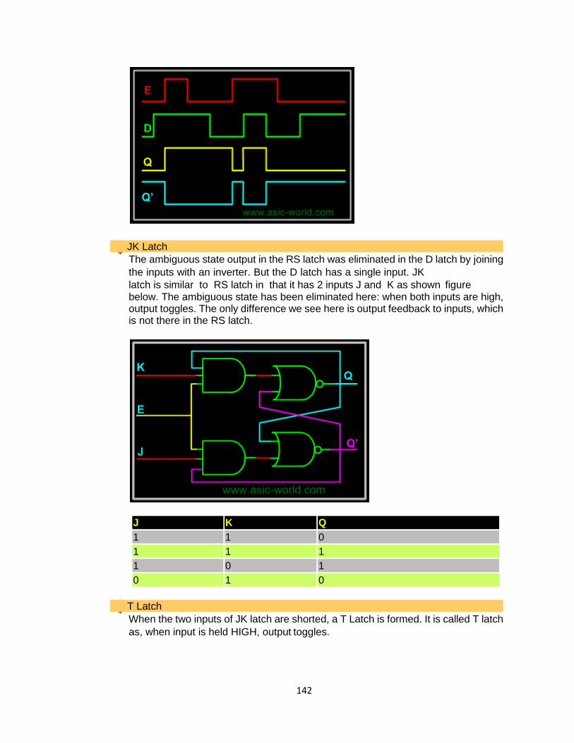
142
142
JK Latch
The ambiguous state output in the RS latch was eliminated in the D latch by joining
the inputs with an inverter. But the D latch has a single input. JK
latch is similar to RS latch in that it has 2 inputs J and K as shown figure below. The ambiguous state has been eliminated here: when both inputs are high, output toggles. The only difference we see here is output feedback to inputs, which is not there in the RS latch.
J K Q
1 1 0
1 1 1
1 0 1
0 1 0
T Latch
When the two inputs of JK latch are shorted, a T Latch is formed. It is called T latch
as, when input is held HIGH, output toggles.
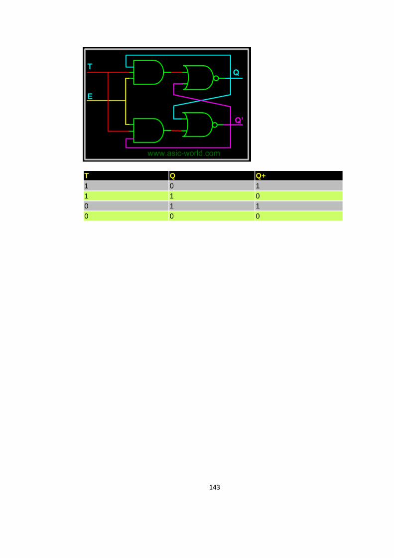
143
143
T Q Q+
1 0 1
1 1 0
0 1 1
0 0 0

144
144
Assignment UNIT 5
Academic Year 2020-21
Course : B.Tech.
Semester/
Section
: III Sem
Subject &
Subject Code
: Digital Electronics & 3CS3-04 Max. Marks : 20
Course Outcomes
CO4 Design various combinational and sequential circuits
Q.
No.
Questions Marks
1. Realise K flip flop using T flip flop. 2
2. Design SR flip flop usingK, T and D flip flop. 2
3. Show how the JK flip flop can be converted to D flip flop with an inverter between J&
K inputs.
2
4. Explain the operation of master slave flip flop and show how the race around condition
is eliminated in it.
2
5. Draw the logic diagram of 4-bit binary ripple down counter using
(i) flip flop that trigger on positive edge transition of clock
(ii) flip flop that trigger on negative edge transition of clock
2
6. Use synchronous design counter procedure to design a 4-bit synchronous down counter
that count through all states from 1111 down to 0000 ( use JK flip flop)
2
7. A 4 bit up/down counter is in down mode and in the 1010 state. On the next clock pulse,
to what state?
2
8. Design Johnson counter. 2
9. Design 5-bit ring counter using JK flip flop 2
10. Explain shift register 2