SOT-23-6L Plastic-Encapsulate MOSFETS
5
FEATURE TrenchFET Power MOSFET APPLICATION Load Switch for Portable Devices DC/DC Converter MARKING Maximum ratings (T a =25℃ unless otherwise noted) Parameter Symbol Value Unit Drain-Source Voltage V DS -12 Gate-Source Voltage V GS ±8 V Continuous Drain Current I D -6 Continuous Source-Drain Diode Current I S -0.8 A Maximum Power Dissipation P D 0.35 W Thermal Resistance from Junction to Ambient(t≤10s) R θJA 357 ℃/W Junction Temperature T J 150 Storage Temperature T STG -50 ~+150 ℃ CJL1206 Dual P-Channel Power MOSFET SOT-23-6L V (BR)DSS R DS(on) MAX I D -12V 45 mΩ@-4.5V -6A 60 mΩ@-2.5V 90 mΩ@-1.8V Equivalent Circuit SOT-23-6L Plastic-Encapsulate MOSFETS JIANGSU CHANGJING ELECTRONICS TECHNOLOGY CO., LTD 1 www.jscj-elec.com Rev. - 1.0
Transcript of SOT-23-6L Plastic-Encapsulate MOSFETS
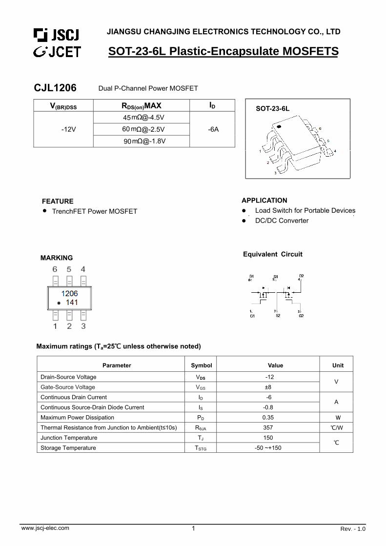
FEATURE TrenchFET Power MOSFET
APPLICATION
Load Switch for Portable Devices
DC/DC Converter
MARKING
Maximum ratings (Ta=25 unless otherwise noted)
Parameter Symbol Value Unit
Drain-Source Voltage VDS -12
Gate-Source Voltage VGS ±8 V
Continuous Drain Current ID -6
Continuous Source-Drain Diode Current IS -0.8 A
Maximum Power Dissipation PD 0.35 W
Thermal Resistance from Junction to Ambient(t≤10s) RθJA 357 /W
Junction Temperature TJ 150
Storage Temperature TSTG -50 ~+150
CJL1206 Dual P-Channel Power MOSFET
SOT-23-6L
V(BR)DSS RDS(on)MAX ID
-12V
45mΩ@-4.5V
-6A 60 mΩ@-2.5V
90mΩ@-1.8V
Equivalent Circuit
SOT-23-6L Plastic-Encapsulate MOSFETS
JIANGSU CHANGJING ELECTRONICS TECHNOLOGY CO., LTD
1www.jscj-elec.com Rev. - 1.0
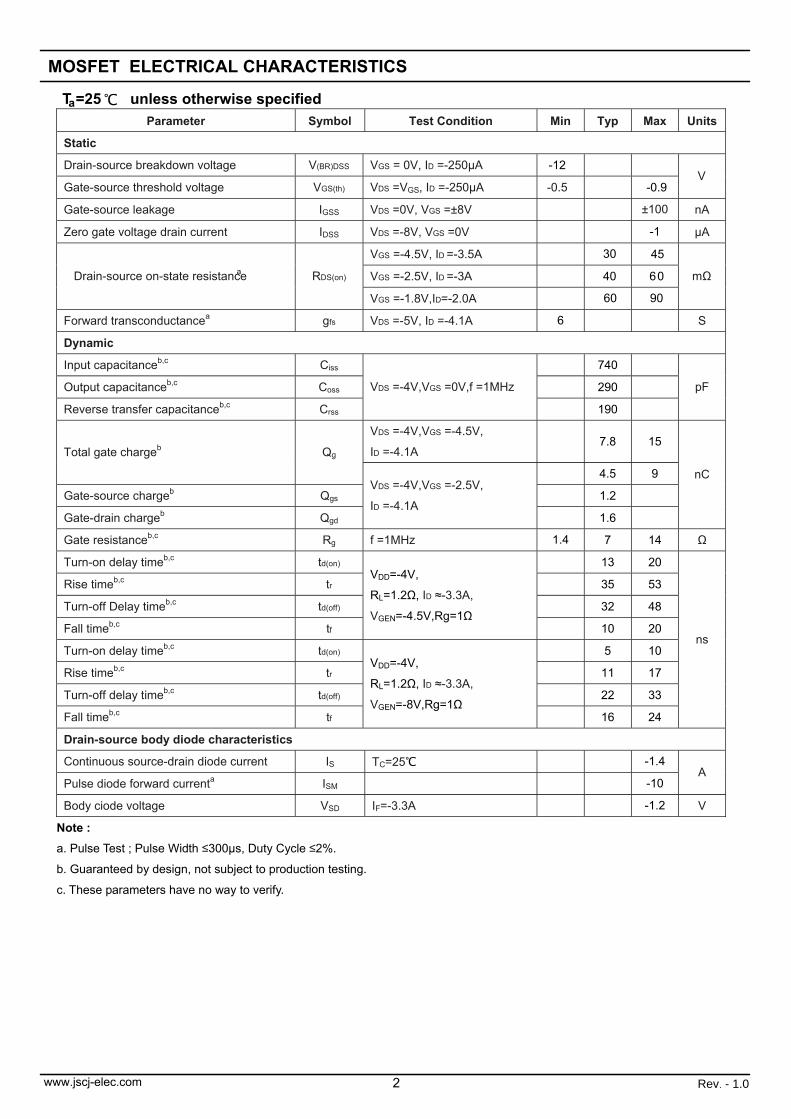
Parameter Symbol Test Condition Min Typ Max Units
Static Drain-source breakdown voltage V(BR)DSS VGS = 0V, ID =-250µA -12 Gate-source threshold voltage VGS(th) VDS =VGS, ID =-250µA -0.5 -0.9
V
Gate-source leakage IGSS VDS =0V, VGS =±8V ±100 nA
Zero gate voltage drain current IDSS VDS =-8V, VGS =0V -1 µA
VGS =-4.5V, ID =-3.5A 30 45
VGS =-2.5V, ID =-3A 40 60 Drain-source on-state resistancea RDS(on)
VGS =-1.8V,ID=-2.0A 60 90
mΩ
Forward transconductancea gfs VDS =-5V, ID =-4.1A 6 S
Dynamic Input capacitanceb,c Ciss 740
Output capacitanceb,c Coss 290
Reverse transfer capacitanceb,c Crss
VDS =-4V,VGS =0V,f =1MHz
190
pF
VDS =-4V,VGS =-4.5V,
ID =-4.1A
7.8 15 Total gate chargeb Qg
4.5 9
Gate-source chargeb Qgs 1.2
Gate-drain chargeb Qgd
VDS =-4V,VGS =-2.5V,
ID =-4.1A 1.6
nC
Gate resistanceb,c Rg f =1MHz 1.4 7 14 Ω
Turn-on delay timeb,c td(on) 13 20
Rise timeb,c tr 35 53
Turn-off Delay timeb,c td(off) 32 48
Fall timeb,c tf
VDD=-4V,
RL=1.2Ω, ID ≈-3.3A,
VGEN=-4.5V,Rg=1Ω 10 20
Turn-on delay timeb,c td(on) 5 10
Rise timeb,c tr 11 17
Turn-off delay timeb,c td(off) 22 33
Fall timeb,c tf
VDD=-4V,
RL=1.2Ω, ID ≈-3.3A,
VGEN=-8V,Rg=1Ω 16 24
ns
Drain-source body diode characteristics
Continuous source-drain diode current IS TC=25 -1.4
Pulse diode forward currenta ISM -10 A
Body ciode voltage VSD IF=-3.3A -1.2 V
Note :
a. Pulse Test ; Pulse Width ≤300µs, Duty Cycle ≤2%.
b. Guaranteed by design, not subject to production testing.
c. These parameters have no way to verify.
MOSFET ELECTRICAL CHARACTERISTICS
T =25 unless otherwise specified a
2www.jscj-elec.com Rev. - 1.0
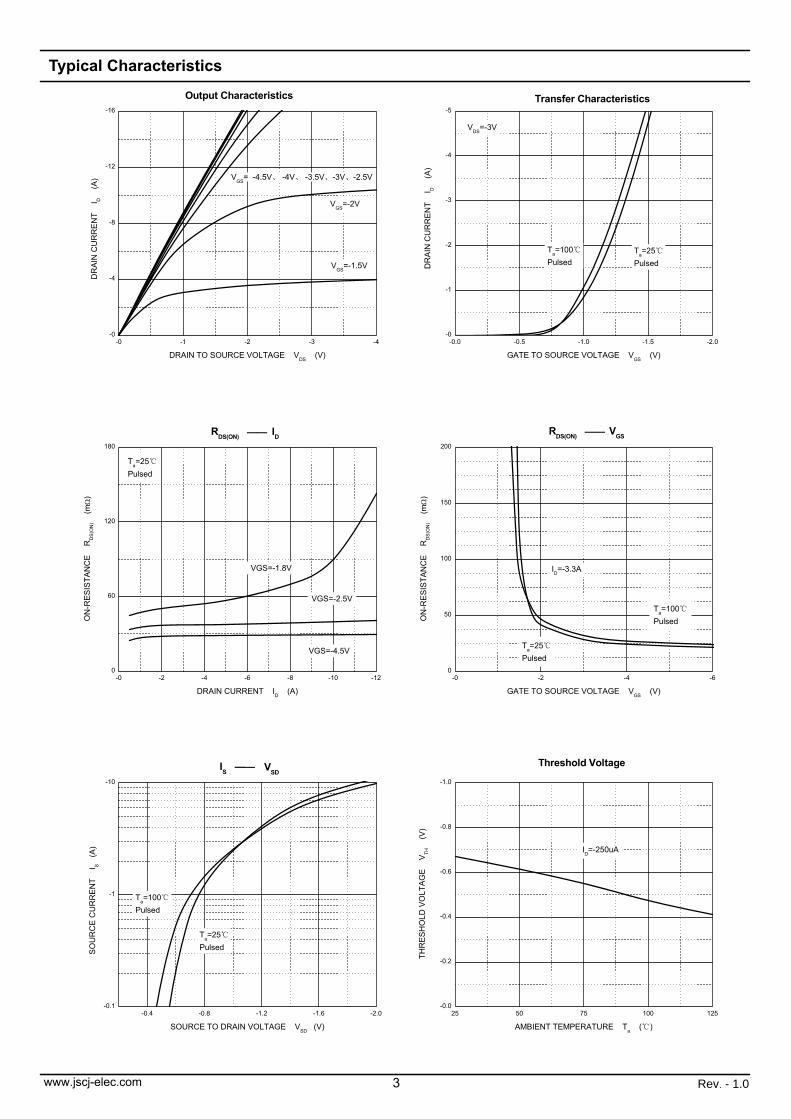
-0.4 -0.8 -1.2 -1.6 -2.0-0.1
-1
-10
-0 -1 -2 -3 -4-0
-4
-8
-12
-16
-0 -2 -4 -6 -8 -10 -120
60
120
180
-0 -2 -4 -60
50
100
150
200
-0.0 -0.5 -1.0 -1.5 -2.0-0
-1
-2
-3
-4
-5
25 50 75 100 125-0.0
-0.2
-0.4
-0.6
-0.8
-1.0
Ta=100Pulsed
VSDIS ——
Ta=25Pulsed
SO
UR
CE
CU
RR
EN
T
I S
(A)
SOURCE TO DRAIN VOLTAGE VSD (V)
VGS = -4.5V、 -4V、 -3.5V、-3V、-2.5V
Output Characteristics
VGS=-1.5V
D
RA
IN C
UR
RE
NT
I D
(A
)
DRAIN TO SOURCE VOLTAGE VDS (V)
VGS=-4.5V
VGS=-2.5V
Ta=25Pulsed
ON
-RES
IST A
NC
E
RD
S(O
N)
(mΩ
)
DRAIN CURRENT ID (A)
ID——RDS(ON)
VGS=-1.8V
Ta=25Pulsed
ID=-3.3A
Ta=100Pulsed
O
N-R
ESIS
TAN
CE
R
DS
(ON
) (m
Ω)
GATE TO SOURCE VOLTAGE VGS (V)
VGS——RDS(ON)
Ta=100Pulsed
Ta=25Pulsed
VDS=-3V
VGS=-2V
DR
AIN
CU
RR
EN
T
I D
(A)
GATE TO SOURCE VOLTAGE VGS (V)
Transfer Characteristics
ID=-250uA
Threshold Voltage
THR
ESH
OLD
VO
LTAG
E
VTH
(V
)
AMBIENT TEMPERATURE Ta ( )
Typical Characteristics
3www.jscj-elec.com Rev. - 1.0
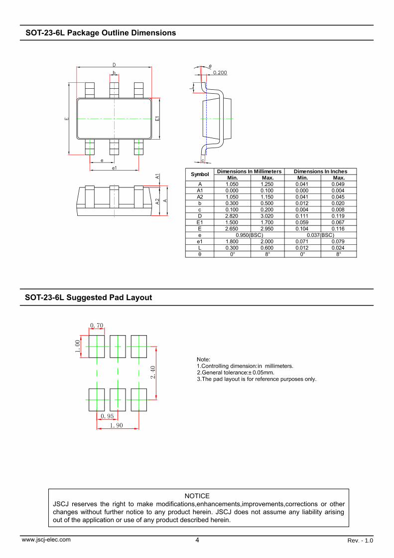
SOT-23-6L Package Outline Dimensions
SOT-23-6L Suggested Pad Layout
Min. Max. Min. Max.A 1.050 1.250 0.041 0.049A1 0.000 0.100 0.000 0.004A2 1.050 1.150 0.041 0.045b 0.300 0.500 0.012 0.020c 0.100 0.200 0.004 0.008D 2.820 3.020 0.111 0.119E1 1.500 1.700 0.059 0.067E 2.650 2.950 0.104 0.116ee1 1.800 2.000 0.071 0.079L 0.300 0.600 0.012 0.024θ 0° 8° 0° 8°
Symbol Dimensions In Millimeters Dimensions In Inches
0.950(BSC) 0.037(BSC)
4www.jscj-elec.com Rev. - 1.0
NOTICE JSCJ reserves the right to make modifications,enhancements,improvements,corrections or other changes without further notice to any product herein. JSCJ does not assume any liability arising out of the application or use of any product described herein.

SOT-23-6L Tape and Reel
5www.jscj-elec.com Rev. - 1.0