Metallization systems for integrated circuits · 2013-08-31 · METALLIZATION SYSTEMS FOR...
26
i NASA TECHNICAL NOTE I?W 1 KIR'I METALLIZATION SYSTEMS FOR INTEGRATED CIRCUITS by Rosemary P. Beat9 Electronics Research Center Cambridge, Mass, 02139 NATIONAL AERONAUTICS AND SPACE ADMINISTRATION WASHINGTON, D. C. JULY 1970 https://ntrs.nasa.gov/search.jsp?R=19700023327 2020-05-06T11:14:55+00:00Z
Transcript of Metallization systems for integrated circuits · 2013-08-31 · METALLIZATION SYSTEMS FOR...

i
N A S A TECHNICAL NOTE
I?W 1
KIR'I
METALLIZATION SYSTEMS FOR INTEGRATED CIRCUITS
by Rosemary P. Beat9
Electronics Research Center Cambridge, Mass, 02139
N A T I O N A L A E R O N A U T I C S A N D S P A C E A D M I N I S T R A T I O N W A S H I N G T O N , D. C. JULY 1970
https://ntrs.nasa.gov/search.jsp?R=19700023327 2020-05-06T11:14:55+00:00Z

TECH LIBRARY KAFB, NM
I111111111111111111111IIIIIllllllllllIll11111 1. Report No. I 2. Government Accession No.
NASA TN D-3866 4. T i t l e and Subtitle
Metallization Systems for IntegratedCircuits
7. Author(s)Rosemary P. Beatty 9. Performing Organization Name and Address
Electronics Research Center Cambridge, Mass.
2. Sponsoring Agency Nome and Address
National Aeronautics and Space Administration
5. Supplementary Notes
6. Abstract
0132bLb 3. Recipient's Catalog No.
5. Report Dote July 1970
6 . Performing Orgonizotion Code
8. Performing Organization Report No. c-112
~
IO . Work Unit No.
125-25-09-14 11. Controct or Grant No.
13. Type of Report and Period Covered
Technical Note
14. Sponsoring Agency Code
Metalliz tion-related failure mechanisms have been shown to be a major cause of integrated circuit failures under accelerated stress conditions. This survey will concentrate on inherent limitations in material combinations and methods of detecting these to provide guidelines for characterization and selection of metallization systems for integrated circuits.
17. Key Words 18. Distribution Stotement-Singlemetal systems*Multilevelmetallization Unlimited*Metallization-related failure mechanisms
19. Security Classif. (of this report) 20. Security Classif. (of this page) 21- No. of Pages 22. Pr ice*
Unclassified Unclassified I 2 3 $3 .OO
METALLIZATION SYSTEMS FOR INTEGRATED CIRCUITS
By Rosemary P. BeattyElectronics Research Center
SUMMARY
Metallization-related failure mechanisms have been shown to be a major cause of integrated circuit failures under accelerated stress conditions. The integrated circuit industry is aware of the problem and is attempting to solve it in one of two ways:(1) better understanding of the aluminum system, which is the most widely used metallization material for silicon integratedcircuits both as a single level metallization and LSI; or (2)evaluating alternative metal systems.
As integrated circuit structures become more complex,additional processing steps are required to obtain multilevel metallization. Low temperature deposition of dielectrics is essential, and etching through to interconnect the levels of metallization is critical. In addition, smaller geometry and closer spacings are required.
Aluminum metallization offers many advantages, but also has limitations particularly at elevated temperatures and high current densities. As an alternative, multilevel systems of the general form, silicon device-metal-inorganic insulator-metal, are being considered to produce large scale integrated arrays.An attempt will be made in this survey to define the merits and restrictions of metallization systems in current usage and systems under development.
INTRODUCTION
Metallization-related failure mechanisms have been shown to be a major cause of integrated circuit failures under accelerated stress conditions. This survey will concentrate on inherent limitations in material combinations, and methods of detectingthese, to provide guide lines for characterization and selection of metallization systems for integrated circuits.
Metallization characterization tests are determined by: (1)properties of metal thin films, (2) metallization requirements,( 3 ) integrated circuit processing, and ( 4 ) long term stress.
Both single- and multilayer-metallization systems will be discussed as such, and as to their applicability to multilevel integrated circuit fabrication. Figure 1 shows a schematic of single metal, multilayer, and multilevel metallization.

s i l i c o n
Metallization system on s i l i c o n device
P* P.Eturied layer
P-type substrate
- . .
Multilayer metallization system
k10,oOO t thermal oxide \ 500 h A 1
WoJu+loSi02 multilevel aystem
Figure 1.- Schematic of single metal, multilayer,and multilevel metallization
2

The basic requirements of any silicon integrated circuit metallization system are:
1. High conductivity (greater than 10 p-ohm-cm);
2. Good adhesion to both silicon, dielectrics, and glass;
3. Low ohmic contact resistance to both n-type and p-typesilicon;
4. System free from degrading intermetallic compoundformation or deleterious silicon reactions duringprocessing or operating life conditions;
5. Amenability to practical production methods of depositionand delineation;
6. Resistance to current-induced metal electromigration;
7 . Freedom from surface instabilities induced by the metal(s) and method of deposition;
8. Compatibility with multilevel processing.
The successful production of large scale integration requires a materials and processing capability for forming metal conductor paths interconnecting the various components. In this respectthe following factors must be taken into account:
1. Electrical constraints;
2. Chemical needs;
3. Metallurgical requirements;
4. Mechanical requirements to provide reliable operation;
5 . The interfaces which must be satisfied by a metallization system.
To consider the electrical requirements, the metallization must be an excellent conductor, since extremely fine lines are required for multilevel, high density, integrated circuits. The thickness of the metal film cannot exceed one-third of thg line width. Therefore, for a 2-p wide conductor line, a 6000-A thick metal is used, which results in an idealized conductor cross-sectional area of 12 x 10-8 cm2. The conducting metal must make ohmic contact to both n-type and p-type silicon. In the case of shallow junctions the emitter and kase p--njunctions will be within 11.1 (or less) of the surface. This requires that the metai used for contact to the silicon will not penetrate more than 100 A.
3

Chemically, the metallization must resist deterioration in oxygen at 5OOOC to survive the post metallization processing steps. The first layer of metallization must act as a reducing agent for silicon dioxide to reproducibly make ohmic contact through the thin layer that readily forms on silicon. When considering the use of multilevel metallization, it is desirable that the metal does not react sufficiently with the dielectric to form conductive electrical paths between the metal layers at the crossover points. It is therefore necessary that the metal be only a slightly reducing agent and that the temperature at which the reduction takes place be reached rapidly and only once to form the ohmic contact.
From a metallurgical standpoint, one mode of failures that has been noted is a mass transfer of the metal conductor when carrying a high current density at elevated temperatures. For example, the mean-time-to-failure for aluminum film conductors carrying 1.5 x l o 6 amp/cm2 at 175OC is about 23 hr. An exchangeof momentum between the electrons and activated metal ions causes the metal ions to be transported in the direction of the electron flow. The result is a depletion of metal at the cathode end where a gradient in current density or temperature exists. The effect is cumulative, further increasing the current densityresulting in an open circuit. As the geometry of the integratedcircuit decreases, current densities exceeding 1 0 6 amp/cm2 mayexist. Since the self-diffusion coefficient for evaporated films decreases when the films become more ordered, the depositiontechniques, which result in well-ordered films whose resistivity approaches that of bulk metal, will also be more stable at high current densities. Refractory metals have low self-diffusion coefficients, which make them attractive for high current densityapplication.
It is also important that metal conductors do not form intermetallics with silicon or with the overlay metal. To minimize these reactions, metals possessing low diffusion coefficients must be used. An equally important consideration is packaging. Both metal components must be sufficiently soft to flow during bonding. Flow by deformation is required to open fresh and, therefore, clean metal surfaces in intimate contact with each other to promote atomic interdiffusion and crystal growth resulting in a weld.
It is desirable for the conductor used in multilayer metallization schemes to utilize a metal which has a coefficient of thermal expansion near to that of silicon. In the application of glass as a protective layer over the conductor, the bulk expansion differential may be sufficient to cause cracking of the dielectric, thus resulting in electrical shorts. The reduction of glass cracking in multilevel metallization requires
4

t h a t t h e m e t a l conductor be a r easonab le match t o t h e c o e f f i c i e n t of expansion o f t h e s i l i c o n and t h e d i e l e c t r i c .
I t i s very impor t an t i n t h e s e l e c t i o n of a m e t a l l i z a t i o n system t o c o n s i d e r t h e p rocess ing s t e p s r e q u i r e d i n t h e f a b r i c a t i o n of an i n t e g r a t e d c i r c u i t . These s t e p s are:
1.
2 .
3.
4.
5.
6.
7.
8.
Depos i t ion of m e t a l l i z a t i o n ( s i l i c o n , c o n t a i n i n g p-n j u n c t i o n s and d i e l e c t r i c s , hea t ed t o 2 0 0 t o 5OOOC p r i o r t o vacuum d e p o s i t i o n and d e p o s i t i o n t i m e s ranging from 1 0 t o 2 0 min f o r each me ta l l a y e r ) ;
H e a t t r e a t m e n t s (5 t o 15 min a t 300 t o 6 O O O C f o r good ohmic c o n t a c t s ) ;
G l a s s d e p o s i t i o n ( 2 0 0 t o 5OOOC f o r 1 0 t o 20 min 1 :
A p p l i c a t i o n of s o l d e r o r e u t e c t i v e bonding m a t e r i a l on back of wafer (5 min a t 400 t o 50OOC);
Bonding c h i p t o header o r package ( 5 m i n a t 4 0 0 t o 500°C) :
Lead bonding (RT t o 350OC);
Sea l ing package ( 5 t o 30 min a t 2 0 0 t o 5OO0C!;
O p e r a t i o n a l l i f e stress tes ts a t e l e v a t e d tempera tures (300OC f o r 1 0 0 0 o r more h o u r s ) .
One of t h e most s t r i n g e n t tes ts i s t h e 3OOOC s t o r a g e t e s t w i t h b i a s v o l t a g e a p p l i e d t o t h e dev ice . Some d e v i c e s o p e r a t i n g a t h igh power r e s u l t i n h igh c u r r e n t d e n s i t i e s and l o c a l i z e d tempera tures t h a t may exceed 500OC.
EVALUATION O F METALLIZATION SYSTEMS
S i n g l e M e t a l Systems
Aluminum i s t h e predominant m e t a l l i z a t i o n system used i n t h e f a b r i c a t i o n of s i l i c o n i n t e g r a t e d c i r c u i t s f o r t h e fo l lowing r easons :
1. H a s a low bu lk r e s i s t i v i t y of 2 . 7 p-ohm-c~rt ( f i l m s c l o s e l y approach t h i s v a l u e ) ;
2 . Is e a s i l y evapora ted ;
5

3. For a r e s i s t i v i t y of 0 . 1 ohm p e r s q u a r e , f i l m s need o n l y be 3000 a;
4 . H a s good adherence t o s i l i c o n and s i l i c o n d i o x i d e ;
5. Has good ohmic c o n t a c t t o bo th p- type and n-type s i l i c o n ;
6 . Is e a s i l y p a t t e r n e d .
Unfo r tuna te ly , i n c e r t a i n a p p l i c a t i o n s , aluminum does posses s u n d e s i r a b l e c h a r a c t e r i s t i c s . For example, aluminum r e a c t s wit.h gold t o form v a r i o u s i n t e r m e t a l l i c compounds which i n c r e a s e cont a c t res is tance and can r e s u l t i n open bonds. T h i s r e a c t i o n takes p l a c e r a p i d l y a t 45OOC and can occur over a p e r i o d of t i m e a t 15OOC. Although t h e i n t e r a c t i o n of t h e m e t a l s c a n be e l i m i n a t e d by us ing u l t r a s o n i c a l l y bonde6 aluminum w i r e s , u l t r a s o n i c bonding demands p r e c i s e equipment and p rocess c o n t r o l . Unlike t h e gold b a l l bonds, t h e u l t r a s o n i c bond of aluminum w i r e t o aluminum m e t a l l i z a t i o n i s weaker than t h e w i r e i t s e l f . The A1-A1 bonds Lsua l ly f a i l a t t h e h e e l of t h e bond where t h e w i r e has been deformed by t h e bonding t o o l . F igu re 2 shows a common p o t e n t i a l f a i l u r e i n u l t r a s o n i c bonds.
F igu re 3 shows ano the r f a i l u r e mode commcnly found i n i n t e g r a t e d c i r c u i t s , which appea r s when alumir,um cGnductors c a r r y c u r r e n t d e n s i t i e s i n excess of l o 5 amp/cm2 a t t empera tures above 1 0 0 O C . The mode of f a i l u r e i s an open c i r c u i t caused by t h e movement of aluminum i o n s i n t h e d i r e c t i o n of t h e e l e c t r o n flow. Voids i n t h e m e t a l , r e s u l t i n g from t h i s p r o c e s s , t end t o grow i n a d i r e c t i o n normal t o t h e c u r r e n t f low. The e f f e c t i s a n accumulat ive one i n c r e a s i n g t h e l o c a l c u r r e n t der , s i ty i n t h e r e g i o n of t h e v o i d , t h u s a c c e l e r a t i n g t h e p r o c e s s . Th i s f r e q u e n t l y occur s i n e m i t t e r s t r i p s where t h e s t r i p t h i c k n e s s i s reduced a s it e x t e n a s over a s t e p i n t h e g l a s s s u r f a c e . A l u m i n u m a t 5OOOC w i l l a t t a c k t h e under ly ing s i l i c o n d i o x i d e and m i g r a t e through t o t h e s i l i c o n ir, a few hours . Even a t t empera tures around 30OoC, ove r long p e r i o d s of t i m e , t h e alumir,um develops h igh c r y s t a l l i n e s p o t s and v o i d s which cause opens i n t h e m e t a l l i z a t i o n . An a d d i t i o n a l concern i s a f a i l u r e mode a s s o c i a t e d wi th A1-Si c o n t a c t s , which r e s u l t s i n t h e growth of e t c h p i t s i n t o t h e s i l i c o n a t t h e p o s i t i v e t e r m i n a l s duriEg h igh c u r r e n t d e n s i t y and tempera ture stress. I t i s s p e c u l a t e d t h a t t h e e t c h p i t format ions are due t o :
1. S o l i d s t a t e d i s s o l u t i o n of s i l i c o n i n t o aluminum t o s a t u r a t e t h e aluminum a t i t s o p e r a t i n g tempera ture ;
2 . T r a n s p o r t of t h e d i s s o l v e d s i l i c o n away from t h e i n t e r f a c e by momentum exchange between thermal a c t i v a t e d
6

Figure 2.- Potential ultrasonic bond failure
( 2 4 0 0 X H O R I Z O N T A L
Figure 3 . - One-mil aluminum strip with void formation due to electromigration
7

- , I
s i l i c o n i o n s and conduct ing e l e c t r o n s enab l ing f u r t h e r s o l i d s t a t e d i s s o l u t i o n of s i l i c o n i n t o aluminum.
Because s i l i c o n w i l l p r e f e r e n t i a l l y e n t e r t h e aluminum from c r y s t a l l i n e d i s l o c a t i o n , r a t h e r t han uni formly ove r t h e s u r f a c e , t h e p r o c e s s r e s u l t s i n t h e format ion of e t c h p i t s i n t o t h e s i l i c o n a t c r y s t a l l i n e d i s l o c a t i o n s . The p r o c e s s can c o n t i n u e u n t i l t h e j u n c t i o n benea th t h e A1-Si c o n t a c t i n t e r f a c e i s e l e c t r i c a l l y s h o r t e d by t h e growth of an e t c h p i t through t h e j u n c t i o n .
Other s i n g l e m e t a l systems p r e s e n t problems i n d e p o s i t i o n t echn iques , adherence t o s i l i c o n d i o x i d e , and h igh r e s i s t a n c e f i l m s .
M u l t i l e v e l M e t a l l i z a t i o n Systems
For t h e r e a s o n s mentioned above, two o r more meta l l a y e r s a r e cons ide red . A composi te - layered m e t a l l i z a t i o n system cons is ts of a m e t a l t h a t adhe res w e l l t o s i l i c o n and s i l i c o n d iox ide and an o v e r l a y of a h igh c o n d u c t i v i t y m e t a l . I n c e r t a i n cases a t h i r d m e t a l may be used t o p r e v e n t d i f f u s i o n o r i n t e r a c t i o n between t h e t o p and bottom metals . One such system u t i l i z e s p la t inum s i l i c i d e , w h i c h posses ses a number of d e s i r a b l e p r o p e r t i e s f o r a n ohmic c o n t a c t t o both n-type and p-type s i l i c o n . The most s t a b l e s i l i c o n h igh s i l i c i d e can be formed by s o l i d -s o l i d r e a c t i o n f a r below t h e me l t ing p o i n t of t h e e u t e c t i c . Th i s i s an impor tan t p o i n t ( a s compared t o aluminum m e t a l l i z a t i o n p r o c e s s i n g ) . P la t inum s i l i c i d e c a n be formed on a t o m i c a l l y c l e a n s i l i c o n s l i g h t l y above 3OO0C, whereas t h e me l t ing p o i n t of t h e eu tec t i c i s 980OC. B u i l t i n t o t h e p r o c e s s i s a h ighe r degree of c l e a n l i n e s s t h a n e x i s t s w i t h o t h e r m e t a l systems. P r i o r t o t h e d e p o s i t i o n o f p l a t inum, t h e chemica l ly-c leaned , s i l i c o n s u r f a c e i s plasma-etched by b a c k s p u t t e r i n g w i t h a rgon i o n s . Th i s produces a plasma ove r t h e s i l i c o n s u b s t r a t e t h a t i s e f f e c t i v e i n removing traces of r e s i d u a l ox ide and contaminat ion which may remain a f t e r chemical e t c h i n g . With ex t remely s m a l l c o n t a c t a r e a s (0 .3 x 0.3-mil windows), t h e a b i l i t y t o ach ieve completely c leaned o u t windows, f r e e of a l l d i e l e c t r i c and o t h e r contaminat i o n , i s ex t remely d i f f i c u l t , however, and a h igh tempera ture h e a t t r e a t m e n t of aluminum c o n t a c t s i s employed i n o r d e r t o i n s u r e "punching through" t h e r e s i d u a l d i e l e c t r i c by t h e aluminum.
The amount of c o n t a c t r e s i s t a n c e and l i n e a r i t y of r e s i s t a n c e in t roduced by a p a r t i c u l a r m e t a l l i z a t i o n p r o c e s s i s an impor tan t p r a c t i c a l problem i n t h e s u c c e s s f u l f a b r i c a t i o n of semiconductor dev ices . A v a i l a b l e d a t a on t h e c o n t a c t r e s i s t a n c e f o r n-type and p-type s i l i c o n are g iven i n Tables I and 11.
One p a r t i c u l a r l y s i g n i f i c a n t a p p l i c a t i o n of platinums i l i c i d e ohmic c o n t a c t s t o both n-type and p- type s i l i c o n has been
8

- - - - - - - - - - - -
- -
TABLE 1.- METAL SILICON CONTACT RESISTANCE IN OHMS,
AREA = 10-4
Metal and Metal + PtSiSi Resistivity,
n - Type Si i
0.001 0.09 0.02 0.08 0.02 0 . 0 2 0 .02 0.01 0.01 6 (R 0.1 5 ( R ) 0.4 2 0.3 4
-
R - cm A1 PtSi Ni I PtSi -Ti ~
p - Type Si
0 .002 0.03 0 . 0 2 0.06 0 . 0 3 0.04 0 . 0 4 0 . 0 4 1 0 . 7 3 ( R ) 1 8 ( R ) 1 0 . 0 8 0 . 5 20 10 8 0 ( R ] l o 200 (R) 1 5
L
( R ) indicates rectifying contact
TABLE 11.- TEMPERATURE STABILITY, CONTACT RESISTANCE ( a )
Si Resistivity Initial Resistivity After 1 5 min at R 45OOC Air Bake
~~
R - cm A1 + PtSi A1 + PtSi - _____ ~~
n - Type Si
0.001 0.08 0.02 0.08 0 . 0 2 4 to 10 ( R ) 0.02 0.01 4 to 9 ( R ) 0.1 5 to 2 0 (R) 0.1 1 5 to 6 0 ( R ) 0.09
p - Type Si
0.002 0.03 0.03 0.02 0.01 0.02 0.5 50 to 70 ( R ) 3 0 25 25
( R ) indicates rectifying contact
9

their incorporation into the design of beam-lead transistors. Prior to a more detailed discussion of beam-lead technology, it should be emphasized that the key contacting areas to active devices are platinum-silicide ohmic contacts. Platinum-silicide ohmic contacts are being used successfully not only on transistor structures but also on insulated gate field transistors utilizingSchottky barrier contacts for source and drain.
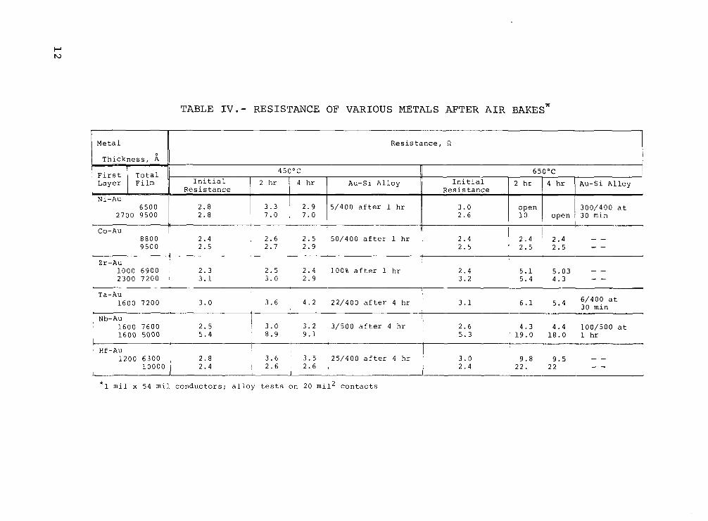
A number of refractory metals combined with gold or silver as conducting metals were investigated, and in the cases of Cr-Au, Ti-Au, and V-Au disregarded for reasons of resistance changes due to interdiffusion or intermetallic formation. In all three cases gold alloyed with the underlying silicon throughthe interface metal. Increasing the thickness of the interface metal delayed the reaction but resulted in a high resistance film. The results of this experimental work are presented in Tables I11 and IV.
Introducing a barrier metal, such as platinum, between the titanium and gold films prohibits the intermetallic formation mentioned previously. This Ti-Pt-Au combination has been used successfully for several years and is known as beam-lead technology. The critical parameter in the Ti-Pt-Au metal system is the platinum thickness. The platinum must be thick enough to avoid pinholes but thin enough to have a minimum of resistance change at elevated temperature operating conditions. A thickness of 1500 to 2000 is a reasonable figure.
Silver has also been used as a barrier between Cr-Au and Ti-Au. The Cr-Ag-Au system is not as thermally stable as Ti-Pt-Au, but is excellent �or low temperature operation.
Chromium-Silver-Gold-Metallization
A study has shown that a Cr-Ag-Au metallization system will be more compatible with future transistor structures than aluminum. In the Cr-Ag-Au system the initial layer of chromium is used to provide the necessary metallization adherence to the silicon dioxide, and the outermost layer of gold is employed as a nonoxidizable bonding surface. An intermediate blended layerof Ag-Au is utilized to separate the chromium from the gold,thereby preventing the occurrence of Cr-Au intermetallic solid solutions which can be difficult to etch. The silver and gold,which make up the current carrying portions of this metallization system, have greater atomic masses, greater activation energies for self-diffusion, and higher melting points than aluminum. These factors suggest that this system should have a better high current density capability than does aluminum. It is also noted that chromium and silver do not react with silicon at temperatures below 600°C, thus forming a barrier which
10

- - - -
- - - -
- -
- - - -
TABLE 111.- RESISTANCE OF VARIOUS METALS AFTER AIR BAKES*
Resistance, 1. Thickness,
A1 7000 2.7 2.6 2.7 _ - _ _ _ -
Cr-Au 2000 6 0 0 0 I 5.8 17.4 19.0 100% at 1 hr - _ - _ _ _
- - _ _ ~ Ti-Au
2000 6500 5 . 4 12 18 100% at 1 hr _ _ _ -
800 9900 1600 6 6 0 0 I 1.7
3.5 3.6 7.1
3.6 5.9
300/400 after 1 hr 1.7 6 . 6 5.6 100% after 30 3.6 8.3 9.5 min
( T i - P t y - G l3000 9 0 0 0 2.9 4 . C 4.3 0/120 after 4 hr _ _ - _
MO-AU I 2100 10,000 2700 7200
W-AU
3.2 3.1
2.5 2.8
2.5 2.8 1 / 4 0 0 after 4 hr
2.1 2.3 2.3 12/400 after 4 3.2
~ 2.7 , 2.8 hr
-------I1 1400 6 6 0 0 2.6 2.6 2.5 2.5
7200 3.4 2.7 2.7 2/400 after 4 hr 3.3
Ti-Mo-Au 500 1500
5500 5 . 6 5.7 5.7 - _ 5.3 I
W-Au-Ti _ _ _ _300 ( T i ) 4.9 3.4 3.2 4.7 2.7 2.6
*1 mil x 50 mil conductors: alloy tests on 20 mil2 contacts
- -
- - - -
r h)
TABLE IV.- RESISTANCE OF VARIOUS METALS AFTER AIR BAKES^
Metal Resis tance, R
T h i c k n e s s , w F i r s t T o t a l 45OOC 65OOC
L a y e r F i l m I n i t i a l Resis tance
2 h r 4 h r Au-Si A l l o y I n i t i a l R e s i s t a n c e
2 h r 4 hr Au-Si A l l o y
N i - A U 11 6 5 0 0 2 . 8 3 . 3 2 . 9 5 / 4 0 0 a f t e r 1 h r 3 . 0 3 0 0 / 4 0 0 a t
2 7 0 0 9 5 0 0 2 . 8 7 . 0 7 . 0 2 . 6
CO-AU
Z r - A u 1 0 0 0 6 9 0 0 I 2 . 3 2 . 5 2 . 4 1 0 0 % a f t e r 1 h r 2 . 4 5 . 1 5 . 0 3 - 2 3 0 0 7 2 0 0 3 . 1 3 . 0 2 . 9 3 . 2 5 . 4 4 . 3
Ta-Au 1 6 0 0 7 2 0 0 3 . 0 3 . 6 4 . 2 2 2 / 4 0 0 a f t e r 4 h r ' 3.1 6 . 1 5.4 6 / 4 0 0 a t3 0 m i n , - ! 7-Nb-Au
3 . 21 6 0 0 7 6 0 0 2 . 5 c'3 / 5 0 0 a f t e r 4 h r 'i 2 . 6 4 . 3 4 . 4 l 0 0 / 5 0 0 a t 1 6 0 0 5 0 0 0 5 . 4 ' 8 . 9 9 . 1 5 . 3 ' 1 9 . 0 1 8 . 0 1 h r
.L__-L,,7-' I' Hf-AU 1 2 0 0 6 3 0 0 , , 2 . 8 3 . 6 ,' 3 . 5 2 5 / 4 0 0 a f t e r 4 h r ' 3 . 0 9 . 8 9.5
1 0 0 0 0 Ij 2 . 4 1 2 . 6 I 2 . 6 , 2 . 4 2 2 . 2 2
* 1 m i l x 5 4 m i l c o n d u c t o r s ; a l l o y tes ts on 2 0 m i l 2 c o n t a c t s

i n h i b i t s t h e d i s s o l u t i o n of t h e s i l i c o n s u b s t r a t e . An e v a l u a t i o n w a s made of t h e r e s i s t a n c e of t h e c o n t a c t s of Cr-Ag-Au t o s i l i c o n us ing aluminum as a comparison and c o n t r o l . Table V and F i g u r e 4 show t h e r e s u l t s of t h e s e measurements.
These r e s u l t s i n d i c a t e t h a t Cr-Ag-Au makes a good, l o w r e s i s t a n c e ohmic c o n t a c t t o n-type s i l i c o n f o r doping l e v e l s g r e a t e r than 1 x 10l8 atoms/cm3, whereas aluminum makes h igh r e s i s t a n c e nonohmic c o n t a c t f o r doping levels less t h a n 4 x 10¹⁸ atoms/cm3. For doping l e v e l s g r e a t e r t han 1 x 10l8 a t o m s / cm3 i n p-type s i l i c o n , t h e Cr-Ag-Au makes a s good or s l i g h t l y b e t t e r c o n t a c t t h a n does aluminum. I n e i t h e r case, by t h e u s e of an enhancement d i f f u s i o n t h e Cr-Ag-Au system can provide b e t t e r ohmic c o n t a c t t o n- type and p-type s i l i c o n than does aluminum.
I t should be noted t h a t , f o r c o n t a c t s made t o p-type s i l i c o n , t h e sp read ing r e s i s t a n c e i s t h e dominant t e r m i n t h e measurements. For n-type s i l i c o n , however, t h e spreading r e s i s t a n c e i s an a p p r e c i a b l e p o r t i o n of t h e measured r e s i s t a n c e v a l u e s on ly f o r s i l i c o n m a t e r i a l s of r e s i s t i v i t y less t h a n 0.005 ohm-cm.
A s tudy w a s made of t h e behavior of t h e Cr-Ag-Au m e t a l l i z a t i o n under h igh c u r r e n t d e n s i t y loads and e l e v a t e d t empera tu res . The exper imenta l p rocedure used i s d e s c r i b e d a s f o l l o w s . The m e t a l l i z a t i o n was d e p o s i t e d on to s u b s t r a t e s of 5000-& S i 0 2 on s i l i c o n wafers . The m e t a l l i z a t i o n c o n s i s t e d of 7 0 0 of C r , and 2500 a of Ag-Au (17 a tomic p e r c e n t Ag) b lend . A f t e r e v a p o r a t i o n , t h e Cr-Ag-Au f i l m w a s e t ched t o form a se t of f o u r conductor s t r i p s , each 54 m i l s i n l e n g t h and 0 . 5 , 1 . 0 , 1 . 5 , and 2 . 0 m i l s i n wid th , r e s p e c t i v e l y . The d i e was assembled on to TO-5 heade r s and t h e me ta l can s e a l e d under a d r y n i t r o g e n ambient. The 2 - m i l s t r i p was used f o r t h e c u r r e n t d e n s i t y exper iments , wh i l e t h e 1 . 5 - m i l s t r i p se rved a s a c o n t r o l t o monitor t h e r e s i s t a n c e change due t o t empera tu re a l o n e . The f i l m t empera tu re was determined from t h e oven tempera ture p l u s t h e tempera ture r i se due t o t h e r e s i s t i v e h e a t i n g of t h e f i l m . A thermal impedance of 190°C/W w a s employed f o r t h e TO-5 header .
The r e s u l t s f o r a t y p i c a l 2 - m i l s t r i p aged f o r 175 h r a t a f i l m tempera ture of 435OC and a c u r r e n t d e n s i t y of 2 x 1 0 6 amp/cm2 are a s fo l lows :
i n i t i a l r e s i s t a n c e ( a t 25OC) = 1 1 . 4 2 R
r e s i s t a n c e d u r i n g t es t ( a t 435OC) = 1 6 . 2 R
f i n a l r e s i s t a n c e ( a t 25OC) = 1 2 . 9 1 R
The c u r r e n t s t r e s s e d s t r i p showed a 1 3 p e r c e n t i n c r e a s e i n r e s i s t a n c e , w h i l e t h e r e s i s t a n c e of t h e a d j a c e n t 1.5-mil c o n t r o l
13

- -
- -
TABLE V.- CONTACT RESISTANCE OF CHROMIUM-SILVER-GOLD AND ALUMIUM TO SILICON
Silicon Resistivity Impurity
R - cm Concentration, atom/cm3-.
p-Type Si 0.001 1 .5 x 1020
0.002 6 . 0 x 1019
0.01 1.0 x 101 9
0.1 6.0 x 10¹⁷
0.3 9 . 0 x 101 6
1.0 1.5 x 10¹⁶
n-Type Si
0.001 1.0 x 10² 0
0 .007 1.0 x 101 9
0.01 5 . 0 x 1018
0.03 1.0 x 10¹⁷
J 0z aL
Ixto-’ K
I x I d a
C 01 0.01 0.1
Aluminum, Cr-Ag-Au,
R - cm2 R - cm 2
1.2 x 1.2 x 4 . 0 x
2.3 3.0
1.1 1.5 4.8
Nonohmic
1.9 x 1.2 x
8.0
Nonohmic 2.0
Nonohmic Nonohmic
1.0
SILICON RESISTIVITY, ohm- cm
Figure 4.- Contact resistance of chromium - silver -gold vs. silicon resistivity
14

strip increased 4 percent during the test. There were no opencircuit failures of the Cr-Ag-Au metallization when stressed at current densities up to 2 x 10⁶ amp/cm2 for 500 hr at film temperatures in excess of 400OC. In fact, microscopic examination of the metallization showed no detectable changes in the films due to this aging treatment. It is of interest to note that the mean-time-to-failure for an equivalent aluminum sampleis less than 8 hr.
The lessening of the electromigration failure effect is the result of several factors. The activation energies for the self-diffusion of silver (1.93 eV) and gold (1.91 eV) are considerably greater than that for aluminum (1.41 eV), which in itself will reduce the electromigration. In addition, while the blending of the silver and the gold increases the resistivity of the films, the resulting decrease of the electron free path will diminish the electromigration effect in the blended structure with respect to either pure silver or pure gold. In general, the resistivityof the blended Cr-Ag-Au is a factor of two greater than that of the evaporated aluminum. However, the ease with which the Cr-Ag-Au is patterned allows the use of thicker Ag-Au layers in order to decrease the film resistance where that may be a consideration. These factors, coupled with the heavy atomic masses and higher melting temperatures of silver and gold, have resulted in a metallization system which has been shown to be capable of carrying heavy current loads for extended periods of time. This system is thus an attractive one for use in power transistor applications where large currents must be carried at high temperatures.
The Cr-Ag-Au metallization has been used for multilayeredmetal structures. Two-layered power transistors and three-layered integrated circuits have been fabricated routinely with the above described metallization. No difficulties are encountered in making ohmic contact between the metal layers. Finally, with the glass deposition techniques used for these multilayered structures, there was no observed tendency for the glass to lift away from the Cr-Ag-Au metallization.
Because of the vulnerability of the silver, high temperature exposure of the metallization to an oxidizing ambient increases the film resistivity. The passivation of the metallization with a glass coating results in a factor of ten improvement in the ability of the Cr-Ag-Au to withstand high temperature oxidation. Extended exposure to temperature above 40OoC results in the golddiffusing through the silver and chromium, whereby it finallyalloys with the silicon.
In summary, the Cr-Ag-Au metallization systemi which can be deposited in a conventional evaporator with little increase in
1 5

processing complexity, has the desirable characteristics of aluminum metallization. It can be patterned more easily than equivalent thicknesses of aluminum. The Cr-Ag-Au has excellent storage characteristics at 3OO0C, and has a much longer meantime-to-failure than does aluminum under high current density,high temperature stress. In addition, measurements show that with the use of an enhancement diffusion the Cr-Ag-Au produces as good or better contact to p-type and n-type silicon than does aluminum. Finally, the absence of significant metallization oxide interaction makes Cr-Ag-Au useful for MOS devices and the ease with which contact is made between layers of this metallization indicates a number of applications for Cr-Ag-Au in multilayered devices.
Molybdenum-Gold Metallization
The Mo-Au system has been found stable to 45OoC, and with adequate molybdenum thickness, alloying of the gold with the silicon is not observed. The Mo-Au metallization is readilypatterned and the contact resistance to the silicon is low. It forms stable thermo-compression bonds, and the system is compatible with glassing processes.
Tests of high current density stress have been significant.Circuits have been operated at elevated temperatures with current densities in excess of 106 amp/cm2. Aluminum migrationis observed, and at current levels of 1 0 6 amp/cm2 and 17OoC, lifetimes of the order of 1000 hr are common. In view of the theory that the electromigration is related to the self-diffusion energy of the system, refractory metal, gold metallization systems should show greatly improved high current performance. This has been confirmed in the Cr-Au, Ti-Au, and Mo-Au systems.
Table VI presents measurements of contact resistance of aluminum and refractory metal gold. The results of high current density tests of various metallizations at 175OC and 1 and 2 x 10⁶ amp/cm2 are shown in Table VII.
BEAM-LEAD TECHNOLOGY
One of the most promising metallization and packaging techniques is known as "beam leads." Beam-lead technology is a process developed to batch-fabricate semiconductor devices and integrated circuits with electro-formed electrodes cantilevered beyond the edge of the silicon. This type of structure simplifies the assembly and interconnection of individual units and integrated circuits, provides its own hermetic seal, and leads to a new class of integrated circuits where isolation is accomplished by etched trenches under the metal interconnections. This structure imposes no electrical penalty on the device, the
1 6

- -
- -
- - - -
TABLE VI.- CONTACT RESISTANCE MEASUREMENTS TO 0 . 0 0 1 ohm-cm p-type SILICON, METALLIZATIONS AT 100 mamp CURRENT LEVEL
Resistance, SZ 45OOC Air Bake, SZ .. .
A1 (evaporated) 0 . 0 4 - 0.10 0 . 0 2 1 - 0.022
Cr-A1 (evaporated) 0 .025 - 0 .042 0.019 - 0.026
Cr-Au (evaporated) 0.007 - 0 .010 0 .007 - 0 .010 0.023 - 0.026 0 .005 - 0.008
Ti-Au (evaporated) 0.014 - 0.019 0.007 - 0.010
Mo-Au (evaporated) 0 . 0 1 1 - 0.030 0.012 - 0.027
Metal Initial Contact After 15 min at
Mo-Au-Mo (evaporated) 0.025 - 0.028
TABLE VI1.--MEAN-TIME-TO-FAILURE AS A FUNCTION OF CURRENT DENSITY FOR VARIOUS METALLIZATIONS
C u r r e n t Mean Time t o F a i l u r e , h r * D e n s i t y ,
106amp/cm 2 A 1 ( e v a p o r a t e d ). - .
A 1 ( s p u t t e r e d )
~ . .
MO-AU ( e v a p o r a t e d )
MO-AU ( s p u t t e r e d )
Cr-Au T i -Au ( e v a p o r a t e d ) ( e v a p o r a t e d )-
1 . 0 580 1 0 0 0 4 2 , 0 0 0 4 7 , 0 0 0 (50) ( 3 4 ) ( 4 0 ) ( 2 0 )
2 . 0 2R _ _ 32,000 2100 (57) (50) (30)
2.8 4 . 0 - _ - _ (10)
3.2 _ _ L
J ( 5 1
3.1 450 (10)
~
*Number i n p a r e n t h e s e s refers t o sample s i z e
1 7
I

p a r a s i t i c c a p a c i t a n c e be ing a lmost e q u i v a l e n t t o a conven t iona l p l a n a r dev ice . B a s i c a l l y t h e p r o c e s s s ta r t s w i t h a s t a n d a r d a r r a y of p l a n a r d e v i c e s o r i n t e g r a t e d c i r c u i t s a f t e r t h e c o n t a c t h o l e s have been e t c h e d through t h e ox ide . P l a t i n u m - s i l i c i d e ohmic c o n t a c t s are formed i n t h e c o n t a c t area, and t i t a n i u m and plat inum l a y e r s ’ are s p u t t e r e d on to t h e s i l i c o n . The gold beam l e a d s a r e e lec t ro- formed, u s ing t h e p la t inum as a base . The excess p la t inum o u t s i d e t h e go ld p a t t e r n s i s removed by r - f d i s c h a r g e e t c h i n g , and t h e t i t a n i u m i s e t ched away. A t t h i s p o i n t t h e wafer i s t u r n e d over and etch-masking p a t t e r n s a r e developed i n r e g i s t r y over t h e m e t a l l i z e d p a t t e r n s on t h e o t h e r s i d e . The unmasked a r e a s are e t ched away, l e a v i n g t h e i n d i v i d u a l d e v i c e s wi th t h e beam l e a d s ex tending beyond t h e edges of t h e s l i ce . With no a d d i t i o n a l p r o c e s s i n g , t h e p rev ious e t c h i n g o p e r a t i o n may be used t o c u t i s o l a t i o n t r e n c h e s i n i n t e g r a t e d c i r c u i t s , r e p l a c i n g i s o l a t i o n d i f f u s i o n s o r s o l i d d i e l e c t r i c i s o l a t i o n .
The beam-lead s t r u c t u r e e l i m i n a t e s t h e need f o r c h i p b raz ing and e x t e r n a l w i r e bonding. With t h e beam-lead d e v i c e f a c i n g t h e s u b s t r a t e , c a n t i l e v e r e d l e a d s ex tending beyond t h e edges of t h e c h i p a r e r e a d i l y a l i g n e d wi th matching p a t t e r n s on t h e s u b s t r a t e and t h e beam l e a d s bonded t o t h e s e p a t t e r n s . The beam l e a d s a r e used a s t h e al ignment gu ide - w i t h m u l t i p l e l e a d s ex tending beyond t h e c h i p where one l e a d a u t o m a t i c a l l y r e g i s t e r s t h e r e s t , s i n c e both t h e beam-lead a r r a y and t h e s u b s t r a t e p a t t e r n are p r e c i s e l y o r i e n t e d w i t h r e s p e c t t o each o t h e r du r ing t h e photol i t h o g r a p h i c o p e r a t i o n . The Au-Au bond i s a very r e l i a b l e m e t a l l u r g i c a l system; t h e r e a r e no ox ide f i l m s t o h inde r t h e bonding, go ld i s one of t h e most d u c t i l e m e t a l s , thermocompression bonding occur s a t low tempera ture (3OO0C), and t h e bond formed i s f r e e of a t t a c k by o x i d a t i o n , g a l v a n i c c o r r o s i o n , o r o t h e r c o r r o s i v e media.
The a p p l i c a t i o n of beam-lead technology t o d i s c r e t e , ch ip-i n t e g r a t e d c i r c u i t s has been a p p l i e d t o two DCTL w i t h t h r e e and f o u r i n p u t s . There a r e seven ,h igh - f r equency s i l i c o n t r a n s i s t o r s ( 3 l e a d s ) and nine,beam-lead, boron-d i f fused s i l i c o n r e s i s t o r s . Seve ra l c i r c u i t s wired as a 3-s tage r i n g o s c i l l a t o r , w i th a f a n - i n and fan-out of 1, y i e l d a measured p ropaga t ion d e l a y of 4 . 2 n sec . Measurements a r e made w i t h a c o l l e c t o r supply v o l t a g e of 5 V , cor respondent t o an average power p e r g a t e of 23 mW. This i s e q u i v a l e n t i n performance t o c i r c u i t s f a b r i c a t e d wi th s t a n d a r d c h i p and l e a d c o n s t r u c t i o n .
Beam-lead t r a n s i s t o r s have been a p p l i e d t o a tan ta lum t h i n -f i l m c i r c u i t , a 3-2 i n p u t g a t e DCTL swi t ch ing c i r c u i t . With t h i s s t r u c t u r e , it i s n o t necessa ry t o b r a z e t h e s i l i c o n c h i p s t o t h e s u b s t r a t e , s u b j e c t i n g p r e c i s e r e s i s t o r s t o t h e bonding tempera ture
18
I

r e q u i r e d f o r e u t e c t i c b r a z i n g . U l t r a s o n i c o r s p l i t - t i p r e s i s t a n c e weld may be employed t o a t t a c h t h e beam-lead d e v i c e s t o t h e m e t a l l i z a t i o n .
S p e c i f i c a p p l i c a t i o n o f beam-lead t echn iques t o mono l i th i c i n t e g r a t e d c i r c u i t s l e a d s t o t h e e t c h i n g away of t h e unwanted s i l i c o n from under t h e beam l e a d s , i s o l a t i o n o f s i l i c o n i s a t t a i n e d , and i n t e r c o n n e c t i o n s are made by beam lead. The on ly c a p a c i t a t i v e coupl ing i s t h e n through t h e s m a l l , m e t a l e l e c t r o d e o v e r l a y ( 0 . 1 0 5 pf t y p i c a l ) . T h i s i s many t i m e s lower than t h e s t r a y capac i t ance i n c u r r e d wi th p-n j u n c t i o n i s o l a t i o n mono l i th i c c i r c u i t s . U l t r ah igh speed swi t ch ing c i r c u i t s are p o s s i b l e w i t h t h i s technique w i t h no i n c r e a s e i n p rocess ing complexi ty . The i s o l a t i o n t r e n c h e s are a u t o m a t i c a l l y formed dur ing t h e s i l i c o n e t c h i n g .
I n t h e beam-lead p r o c e s s p la t inum s i l i c i d e i s used as t h e ohmic c o n t a c t ma te r i a l . I t i s one of t h e most s t a b l e compounds of s i l i c o n , i s c o r r o s i o n r e s i s t a n t , i s a s o l i d phase up t o 98OoC, has o p t i c a l r e f l e c t i v i t y d i f f e r e n t from e i t h e r s i l i c o n o r p la t inum, and forms ohmic c o n t a c t t o heavily-doped s i l i c o n . T o form t h e compound i n c o n t a c t h o l e s , plat inum i s s p u t t e r e d o n t o t h e whole s l i c e a f t e r t h e c o n t a c t h o l e s a re opened i n t h e oxide and hea ted t o 7OO0C, w h i l e s t i l l i n an i n e r t atmosphere. The plat inum i n t h e h o l e s w i l l r eac t w i t h t h e s i l i c o n t o form P t g S i 2 , which i s a s o l i d phase and w i l l n o t b a l l up o r c r e e p beyond t h e edges o f t h e c o n t a c t h o l e s as a l i q u i d e u t e c t i c w i l l . I n a d d i t i o n , t h e s i l i c i d e i s a d i f f e r e n t c o l o r from plat inum and can be e a s i l y d i s t i n g u i s h e d under a microscope. The nex t operat i o n i s t o apply a m a t e r i a l t h a t w i l l bond t o both t h e S i 0 2 and t h e P t g S i 2 and s e r v e a s an e l e c t r i c a l connec t ion t o t h e e x t e r n a l c i r c u i t r y . N o s i n g l e element w i l l s a t i s f y a l l t h e s e c o n d i t i o n s : however, a composite l a y e r e d s t r u c t u r e c o n s i s t i n g of Ti-Pt-Au has been s u c c e s s f u l l y employed. The f i r s t l a y e r , t i t a n i u m , i s chosen because of i t s h igh oxygen a c t i v i t y , r e f r a c t o r y n a t u r e , and a b i l i t y t o abso rb a lmost h a l f i t s weight i n r e a c t i o n p roduc t s i n t e r s t i t i a l l y (commonly known a s g e t t e r i n g ) . Also , it forms a n a t u r a l ox ide which i s comple te ly p a s s i v a t i n g a t tempera tures up t o 4 0 0 O C . Although o t h e r m e t a l s such as zirconium and hafnium would probably be adequate , s u c c e s s f u l p r i o r expe r i ence w i t h t i t a n i u m ac t ive m e t a l , semiconductor c o n t a c t on d e v i c e s , such as sha l low j u n c t i o n s o l a r ce l l s f o r communication s a t e l l i t e s and h igh frequency s i l i c o n t r a n s i s t o r s , makes t i t a n i u m a l o g i c a l cho ice f o r t h e ox ide bonding l a y e r .
Gold i s chosen as t h e o u t e r l a y e r because of i t s extreme r e s i s t a n c e t o c o r r o s i o n , ease of bonding, low y i e l d p o i n t , h igh e l o n g a t i o n ( a l lows f o r thermal expansion mismatch w i t h t h e s i l i c o n s u b s t r a t e ) , and s u i t a b i l i t y f o r h igh r e s o l u t i o n e lec t ro- forming . However, g o l d i s a m e t a l l u r g i c a l l y react ive m a t e r i a l and reacts
19

with titanium chemically at relatively low temperatures to form compounds which have none of the desirable characteristics of the individual metals.
This leads to the use of the metal in the middle layer;platinum is chosen as a filler because of its inertness, ease of bonding the gold outer layer, and the low diffusion coefficient of gold into platinum. The method used to deposit the 0.5-mil thick, gold beam leads is electro-forming, the build-up of material by electrdplating in selected areas. This technique has been developed to the point where extremely small geometries are feasible. The use of high resolution KPR dimensions under 0.2 mil is possible. The electrode fingers are etched to a thickness of 0.2 mil, thinner than the 0.5-mil thick, beam leads allowing the close spacing necessary for high frequency operation.
Beam-lead devices have been centrifuged to 135,000 g without failure. Bending tests performed on the leads have yielded twenty 90" bends before breakage. Corrosion testing for periods up to 1000 hr in 36OOC steam and 35OOC wet NaCl has revealed no physical or electrical degradation of beam leads. In addition, temperature cycling and galvanic corrosion aging have been equally harmless. As a by-product of the metallization procedurePt-Ti-Pt-Au, there is considerable enhancement of surface stability and junction quality. This is attributed to the use of sputtered titanium, a highly energetic gettermetal particularlyfor p-n-p transistors which are extremely sensitive to collector channel formation. Forward junction characteristics have been monitored during aging in hot corrosive atmospheres. Typicalresistance changes on contact areas of 0.2 x 1.6 mil are under 0.1 ohm after 1000 hr in 35OOC air or steam. Obviously no problem has arisen with this metallurgical system since if formed at any of the metal interfaces would yield an increase in contact resistance or would require burning-in. In conclusion, beam leads, as a semiconductor interconnection technique, lend themselves to high frequency, silicon switching transistors and ultrahighspeed integrated circuits. Beam leads have been shown to be rugged; units have survived corrosive atmospheres and 135,000 gcentrifuging. This structure imposes no electrical penalty;parasitic capacitance (under 0.05 pf per lead) is equivalent to wire-bonded and brazed-welded assembly. The beam-lead conceptis applicable to many other electronic devices as well. In addition, the electro-formed leads are not required to be of constant cross section. They can taper out as they leave the silicon surface for lower inductance, stripline impedancematching, and even better heat conductance. Isolation for integrated circuits is accomplished as a by-product of the structure. Parasitic capacitance has been shown to be negligible and switch-in times are comparable to equivalent chip-and-wirecircuitry. This has been achieved with no increase in processing
20

complexi ty over d i s c r e t e d e v i c e s The m e t a l l i z i n g procedures developed t o f a b r i c a t e beam-lead d e v i c e s y i e l d an i n c r e a s e i n device- r e l i a b i l i t y ; c o n t a c t r e s i s t a n c e i s - m a i n t a i n e d a t a low v a l u e du r ing s t r i n g e n t a c c e l e r a t e d ag ing tests; and p a s s i v a t i o n of j u n c t i o n and s u r f a c e s has been enhanced. I n a d d i t i o n , glow d i s c h a r g e e t c h i n g has been developed, a l lowing t h e des ign of p h o t o r e s i s t produced geometr ies (down t o 1 11) of i n e r t m a t e r i a l s such as rhodium and i r i d i u m , compat ib le w i t h normal d e v i c e proc e s s i n g . Electro-formed go ld p a t t e r n s of h igh r e s o l u t i o n are employed a s s t a n d a r d procedure .
Paladium has been s u b s t i t u t e d f o r p la t inum i n beam-lead f a b r i c a t i o n of d e v i c e s which could be damaged by s p u t t e r i n g o r electron-beam d e p o s i t i o n t echn iques . Paladium s i l i c i d e has e s s e n t i a l l y t h e same chemical and m e t a l l u r g i c a l p r o p e r t i e s as plat inum s i l i c i d e and can be evapora ted from a h igh p u r i t y t u n g s t e n c o i l . Rhodium i s a l s o a n a l t e r n a t e f o r p la t inum i n beam-lead p rocess ing .
Gold beam l e a d s have r e c e n t l y been cha l l enged both i n t h i s coun t ry and abroad. I t i s s a i d t h a t aluminum beam l e a d s have a l l t h e advantages of go ld beam l e a d s . A d d i t i o n a l l y , t hey a r e easy t o bond u l t r a s o n i c a l l y . The weld i s performed wi thou t h e a t i n g , and t h e r e are no r e l i a b i l i t y problems due t o c o n t a c t of d i s s i m i l a r m e t a l s . T e s t c i r c u i t s , comprised of t h r e e swi t ch ing t r a n s i s t o r s , each welded by t h r e e u l t r a s o n i c bonds upon a t h i n f i l m and molded i n a n epoxy, have been s u b j e c t e d t o d i f f e r e n t t r e a t m e n t s w i t h t h e fo l lowing r e s u l t s :
1. Thermal f a t i g u e of 2 3 , 0 0 0 c y c l e s - no f a i l u r e s ;
2 . Thermal shock from 1 0 0 ° C t o -4OOC - no f a i l u r e s ;
3. Humidity tes ts a t 40°C i n an ambient of 9 0 t o 9 5 % r e l a t i v e humidi ty - no r e j e c t s on 4 0 c i r c u i t s a f t e r 8 0 0 0 h r ;
4 . Opera t ing l i f e t e s t a t 85OC wi th swi t ch ing t i m e s i n t h e frequency range of 1 MHz - no f a i l u r e s a f t e r 2 5 0 h r .
Although comparat ive c o s t f i g u r e s are n o t a v a i l a b l e a t t h i s t i m e , it i s r easonab le t o assume t h a t aluminum beam l e a d s could be a t t r a c t i v e from t h a t s t a n d p o i n t al.50.
As an o v e r a l l summary, r e s i s t a n c e changes a t e l e v a t e d t empera tu res , adherence p rope r t i . e s , and f a b r i c a t i o n d i f f i c u l t i e s i n d i c a t e t h a t no one system w i l l m e e t a l l m e t a l l i z a t i o n r e q u i r e ments. W e can d i v i d e t h e systems which m o s t n e a r l y m e e t t h e s e requi rements i n t o t w o g roups :
2 1

- - - - - -
- -
1. Low temperature applications, beam-lead or plasticencapsulation;
2. High temperature and long processing; e.g. LSI, multilayer systems.
The combination that could be useful as a substitute for aluminum in these two groups are:
1. For beam leads and plastics; Ti-Pt-Au, Ti-Pd-Au, Ti-W-Au, Ti-Pt, and Ti-Rh;
2. Multilayer LSI; Ti-Mo-Au, Ti-W,Au, Ti-Pt-Cr, Ti-Ag, or Cr-Ag.
This analysis is taken from the data presented
TABLE VII1.- SUMMARY OF RESISTANCE
Metals Examined
A1 Ti-Pt Ti-Rh Ti-Pt-Au Ti-Ag-AuTi-Mo-Au Ti-AgCr-Ag-AuW-AU Zr-Au Nb-AU Ni-Au-CO-AU V-AU Ta-Au Cr-Au Ti-Au Mo-Au Hf-AU
AND AU-SI ALLOYING
Increase in Resistance ( 2 hr at 45OOC)
... .. ~ - -.
0 0 0
50% 100% 0
5-10% 100% 0 50% 100% 100%
50% 100% 50% 100% 100%
0 50%
in Table VIII.
CHANGE
Au-Si Alloying (1 hr at 45OOC)
No No No No No
Yes No Some Some Yes Some Yes Yes No Some
It is evident that such composite films are more complexthan aluminum to deposit and difficult to pattern; but the versatility of new sputtering techniques in both depositing and patterning present attractive possibilities. Also the excellent
2 2

characteristics of refractory noble metal systems with respect to shallow penetration into silicon, excellent resistance to deterioration in adverse environments, and greatly increased current carrying lifetime make their usage most attractive on high frequency, high power devices and large scale integration.
CONCLUSION
In an industry such as integrated circuits, where the technology progresses so rapidly there are probably no two manufacturers who use exactly the same processing to fabricate similar type circuits, the interpretation of reliability data from manufacturer to manufacturer is difficult to attain. In cases where the development of a process has been difficult, and therefore slow, the engineers have designed around this deficiency.This sort of procedure may or may not directly affect reliability;regardless of processing procedures, the specific integratedcircuit structure and design can be important factors in determining whether a given metallurgical reaction results in significant degradation of the device characteristics. We have seen from the foregoing discussion that there is one very importantconclusion that can be drawn. Most failures observed in presently available integrated circuits at low stress conditions are due to manufacturing defects rather than inherent limitations of the metallurgical systems. If integrated circuits are subjected to stresses far in excess of their ratings, the observed failures will be primarily due to inherent limitations of the materials used. Such inherent failure mechanisms, however, are not necessarily due to mechanisms which are important in terms of reliability of devices under normal usage conditions.
NASA-Langley, 1970 -9 c-112 23

- -
AERONAUTICSNATIONAL AND SPACE ADMINISTRATION WASHINGTON,D. C. 20546
OFFICIAL BUSINESS FIRST CLASS MAIL
POSTAGE A N D FEES PAID NATIONAL AERONAUTICS AN
SPACE ADMINISTRATION
0 4 U 001 3 4 51 30s 70185 00903
A I R FORCE WEAPONS L A B O R A T O R Y /WLOL/ K I K T L A N D AFE, NEW M E X I C O 87117
P ~ ~ T M A S T E R : If Undeliverable ( Section 158 Postal Manual) Do Not Recur
- .. . - ~ . .~ -.. - .-
“The aeroriciiitical diad space rictii’ities of the United States shall be condzicted so as t o contribnte . . . t o the expansion of hziiiian k n o d edge of pheizonie‘elza i~ the atmosphere and space. The Admiizistration shall provide for the widest practicable and appropriate disseriii?za!ioii of iiiforiiintioia coriceriiing its actiiities and the r e s d t s thereof.’’
-NATIONALAERONAUTICSA N D SPACE ACT OF 1958
NASA SCIENTIFIC AND TECHNICAL PUBLICATIONS
TECHNICAL REPORTS: Scientific and technical information considered important, complete, and a lasting contribution to existing knowledge.
TECHNICAL NOTES: Information less broad in scope but nevertheless of importance as a contribution to existing knowledge.
TECHNICAL MEMORANDUMS: Information receiving limited distribution because of preliminary data, security classification, or other reasons.
CONTRACTOR REPORTS: Scientific and technical information generated under a NASA contract or grant and considered an important contribution to existing knowledge.
TECHNICAL TRANSLATIONS: Information published in a foreign language considered
/to merit NASA distribution in English.
SPECIAL PUBLICATIONS: Information derived from or of value to NASA activities. Publications include conference proceedings, monographs, data compilations, handbooks, sourcebooks, and special bibliographies.
TECHNOLOGY UTILIZATION PUBLICATIONS: Information on technology used by NASA that may be of particular interest in commercial and other non-aerospace applications. Publications include Tech Briefs, Technology Utilization Reports and Notes, and Technology Surveys.
Details on the availability of ihese publications may be obtained from:
SCIENTIFIC AND TECHNICAL INFORMATION DIVISION
NATIONAL AERONAUTICS AND SPACE ADMINISTRATION Washington, D.C. 20546