Planar Metallization Failure Modes in Integrated Power
160
Planar Metallization Failure Modes in Integrated Power Electronics Modules By Ning Zhu Dissertation submitted to the faculty of the Virginia Polytechnic Institute and State University in partial fulfillment of the requirements for the degree of DOCTOR OF PHILOSOPHY In ELECTRICAL ENGINEERING Dr. J.D. van Wyk Dr. Z.X. Liang Dr. W.G. Odendaal Dr. G.Q. Lu Dr. Carlos T A Suchicital Dr. Michael C. Shaw April 14, 2006 Blacksburg, Virginia Keywords: Planar Metallization, Failure Mode, Integrated Power Electronics Modules, Intrinsic Residual Stress, Thermo-mechanical Stress, Peel Stress, In-plane Stress, Power Cycling Test, Temperature Cycling Test Copyright©2006, Ning Zhu
Transcript of Planar Metallization Failure Modes in Integrated Power
Planar Metallization Failure Modes in Integrated
Power Electronics Modules By
Ning Zhu
Dissertation submitted to the faculty of the Virginia Polytechnic Institute and State
University in partial fulfillment of the requirements for the degree of
DOCTOR OF PHILOSOPHY
In
ELECTRICAL ENGINEERING
Dr. J.D. van Wyk
Dr. Z.X. Liang
Dr. W.G. Odendaal
Dr. G.Q. Lu
Dr. Carlos T A Suchicital
Dr. Michael C. Shaw
April 14, 2006
Blacksburg, Virginia
Keywords: Planar Metallization, Failure Mode, Integrated Power Electronics Modules,
Intrinsic Residual Stress, Thermo-mechanical Stress, Peel Stress, In-plane Stress, Power
Cycling Test, Temperature Cycling Test
Copyright©2006, Ning Zhu
Planar Metallization Failure Modes in Integrated Power Electronics Modules
By
Ning Zhu
J.D. van Wyk, Chairman
Electrical Engineering
Abstract
Miniaturizing circuit size and increasing power density are the latest trends in modern
power electronics development. In order to meet the requirements of higher frequency
and higher power density in power electronics applications, planar interconnections are
utilized to achieve a higher integration level. Power switching devices, passive power
components, and EMI (Electromagnetic Interference) filters can all be integrated into
planar power modules by using planar metallization, which is a technology involving
electrical, mechanical, material, and thermal issues. By processing high dielectric
materials, magnetic materials, or silicon chips using compatible manufacturing
procedures, and by carefully designing structures and interconnections, we can realize the
conventional discrete inductors, capacitors, and switch circuits with planar modules.
Compared with conventional discrete components, the integrated planar modules have
several advantages including lower profiles, better form factors, and less labor-intensive
processing steps. In addition, planar interconnections reduce the wire bond inductive and
resistive parasitic parameters, especially for high frequency applications.
However, planar integration technology is a packaging approach with a large contact
area between different materials. This may result in unknown failure mechanisms in
power applications. Extensive research has already been done to study the performance,
processing, and reliability of the planar interconnects in thin film structures. The
thickness of the thin films used in integrated circuits (IC) or microelectronics applications
ranges from the magnitude of nanometers to that of micrometers. In this work, we are
iii
interested in adopting planar interconnections to Integrated Power Electronics Modules
(IPEM). In Integrated Power Electronics Modules (IPEMs), copper traces, especially bus
traces, need to conduct current ranging from a few amps to tens of amps. One of the
major differences between IC and IPEM is that the metal layer in IPEMs (normally
>75µm) is much thicker than that of the thin films in IC (normally <1µm). The other
major difference, which is also a feature of IPEM, is that the planar metallization is
deposited on different brittle substrates. In active IPEM, switching devices are in a bare
die form with no encapsulation. The copper deposition is on top of the silicon chips and
the insulation polyimide layer. One of the key elements for passive IPEM and the EMI
IPEM is the integrated inductor-capacitor (LC) module, which realizes equivalent
inductors and capacitors in one single module. The deposition processes for silicon
substrates and ceramic substrates are compatible and both the silicon and ceramic
materials are brittle. Under high current and high temperature conditions, these copper
depositions on brittle materials will cause detrimental failure spots.
Over the last few years, the design, manufacture, optimization, and testing of the
IPEMs has been developed and well documented. Up to this time , the research on failure
mechanisms of conventional integrated power modules has led to the understanding of
failures centered on wire bond or solder layer. However, investigation on the reliability
and failure modes of IPEM is lacking, particularly that which uses metallization on brittle
substrates for high current operations. In this study, we conduct experiments to measure
and calculate the residual stresses induced during the process. We also, theoretically
model and simulate the thermo-mechanical stresses caused by the mismatch of thermal
expansion coefficients between different materials in the integrated power modules. In
order to verify the simulation results, the integrated power modules are manufactured and
subjected to the lifetime tests, in which both power cycling and temperature cycling tests
are carried out. The failure mode analysis indicates that there are different failure modes
for copper films under tensile or compressive stresses. The failure detection process
verifies that delamination and silicon cracks happen to copper films due to compressive
and tensile stresses respectively.
This study confirms that the high stresses between the metallization and the silicon are
the failure drivers in integrated power electronics modules.. We also discuss the driving
iv
forces behind several different failure modes. Further understanding of thesefailure
mechanisms enables the failure modes to be engineered for safer electrical operation of
IPEM modules and helps to enhance the reliability of system-level operation. It is also
the basis to improve the design and to optimize the process parameters so that IPEM
modules can have a high resistance to recognized failures.
v
Acknowledgements
I would like to give my deepest appreciation to my advisor, Dr. J.D. van Wyk, for
embarking with this project and unconditionally supporting me to complete this study.
With his greatest patience, he leads me to this very interesting area, about which I have
great passion finally, although knew nothing from the beginning. It is such a great
experience to be his student for these years. Without him, I cannot get so far. The spirit
and methodology he passed on us will benefit me in my whole life.
Thank you, Dr. Z. X .Liang, for giving me hands on helps almost anytime I need and
anywhere I can find you. Thank you for your smart ideas and encouragements throughout
my research. I also want to thank Dr. Michael C. Shaw, Dr. G.Q. Lu, Dr. Carlos T A
Suchicital, and Dr. W.G. Odendaal to share their research results with me, provide
important technical inputs and resources, and to spend time with me for further
improvements.
I would like to thank all the stuff and faculties in CPES for providing us this good
research and education environment. Thank you for my colleagues in CPES. You always
let me feel at home.
Very special thanks to Prof. Liu Dichen, who is my advisor of my master’s degree.
He is the one introduce me into power electronics area and encourage me to pursue
further educations.
Finally, I need to thank my family. That is where I came from and who I am. My
parents taught me to be gentle, yet be strong, to be smart, but not aggressive. Always be
prepared and look forward for better future especially in hard times. I am proud to be
their daughter.
To all the friends, thank you!
Ning Zhu
April 2006
Blacksburg, VA
vi
Table of Contents
Abstract ........................................................................................................ii
Acknowledgements ......................................................................................v
List of Figures ..............................................................................................x
List of Tables ............................................................................................xvii
Chapter 1 Introduction..........................................................................1
1.1 High density integration trends in power electronics applications ..................... 1
1.2 Current interconnection technologies ................................................................. 4
1.2.1 Wire bonding .............................................................................................. 4
1.2.2 Ball grid array ............................................................................................. 6
1.2.3 Planar metallization interconnection........................................................... 7
1.3 Applications of the planar interconnect technology ........................................... 9
1.3.1 Embedded Power modules.......................................................................... 9
1.3.2 Integrated power passive modules ............................................................ 11
1.3.3 Integrated EMI filters................................................................................ 16
1.4 Aim of this study............................................................................................... 18
1.4.1 Summary of related research .................................................................... 18
1.4.2 Research work covered in this study ........................................................ 20
Chapter 2: Metal Films on Brittle Substrates in IPEMs....................22
2.1 Fabrication processes of integrated modules .................................................... 22
2.1.1 Integrated active modules (Embedded Power) ......................................... 22
2.1.2 Integrated passive modules ....................................................................... 25
2.1.3 Integrated EMI filters................................................................................ 27
vii
2.2 Metal Films on Brittle Substrates in IPEMs ..................................................... 28
2.3 Interfaces properties.......................................................................................... 30
2.3.1 DBC Cu-Alumina interface ...................................................................... 32
2.3.2 Inter-metallic interfaces ............................................................................ 32
2.3.3 Surface roughness of different substrates ................................................. 35
2.4 Mechanical properties of electroplated Cu film................................................ 37
2.5 Effect of film intrinsic residual stress ............................................................... 41
Chapter 3: Intrinsic Residual Stress ....................................................43
3.1 Introduction and Literature Review.................................................................. 43
3.2 Measurement of Intrinsic Residual Stress in Glass-metal Structure................. 45
3.2.1 Sample preparation ................................................................................... 45
3.2.2 Measuring the bending of glass-copper structure ..................................... 49
3.2.3 Calculation of the intrinsic residual stress ................................................ 51
3.3 Possible methods to minimize the residual stress ............................................. 53
3.3.1 Optimize electroplating parameters .......................................................... 53
3.3.2 Annealing of the residual stress ................................................................ 54
3.4 Chapter review.................................................................................................. 55
Chapter 4: Thermo-mechanical Stresses in IPEMs............................56
4.1 Temperature Distribution in Embedded Power Module................................... 56
4.1.1 Simulation and experimental results......................................................... 56
4.1.2 Time constant of simplified structure ....................................................... 58
4.2 Thermo-mechanical Stress in Simplified Structure .......................................... 61
4.2.1 Von Mises stress ....................................................................................... 61
viii
4.2.2 In-plane stress ........................................................................................... 64
4.2.3 Peel stress.................................................................................................. 70
4.2.4 Shear stress................................................................................................ 76
4.3 FEM modeling and simulation in Embedded Power multi-layer structure ...... 77
4.4 Thermo-mechanical stress investigation in passive modules ........................... 80
4.5 Chapter Review................................................................................................. 86
Chapter 5: Power Cycling and Temperature Cycling Test................88
5.1 Embedded Power modules power cycling test ................................................. 88
5.1.1 Sample preparation ................................................................................... 88
5.1.2 Power cycling test setup and test results................................................... 90
5.1.3 Failure mode analysis for Embedded Power module after power cycling
test 92
5.2 Embedded Power modules temperature cycling test ........................................ 94
5.2.1 Temperature cycling test setup and test results......................................... 94
5.3 Effect of contact pattern on Embedded Power maximum working temperature
96
5.4 Integrated power passive modules power cycling test.................................... 103
5.4.1 Sample preparation ................................................................................. 103
5.4.2 Test setup and test results ....................................................................... 104
5.4.3 Failure mode analysis for integrated passive modules ........................... 106
5.5 Chapter review................................................................................................ 107
Chapter 6: Optimization Design in Simplified Structures ...............109
6.1 Design guidelines for optimized peel stress and in-plane stress..................... 109
ix
6.1.1 Thickness ratio ........................................................................................ 110
6.1.2 Critical size of contact pattern ................................................................ 114
6.1.3 Length ratio............................................................................................. 115
6.1.4 Adhesion layer material selection........................................................... 117
6.1.5 SiC and Si ............................................................................................... 118
6.2 Chapter review................................................................................................ 121
Chapter 7: Summary and future work ..............................................123
7.1 Summary ......................................................................................................... 123
7.2 Future work..................................................................................................... 125
References.................................................................................................127
Appendix A: E. Suhir’s stress model.....................................................134
Appendix B: Wang’s stress model ..........................................................137
Appendix C: Related publications..........................................................140
Vita............................................................................................................142
x
List of Figures
Figure 1.2.1 Power modules using wire bonding interconnection...................................... 5
Figure 1.2.2 Schematic of a BGA module.......................................................................... 6
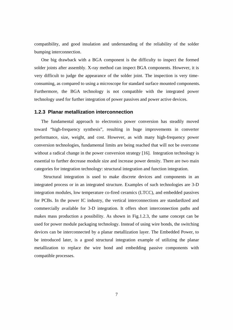
Figure 1.2.3 Cross section schematic of a 3-D integration module .................................... 8
Figure 1.3.1Structural schematic of the Embedded Power module.................................. 10
Figure 1.3.2 Integrated power electronics module realized by Embedded Power
technique. .................................................................................................................. 10
Figure 1.3.3 Exploded view of the Embedded Power module ......................................... 11
Figure 1.3.4 1kW integrated DC/DC converter; (a)Embedded Power module;(b) circuit
diagram ..................................................................................................................... 12
Figure 1.3.5 Embedded decoupling capacitor to decrease the current loop (a) Decoupling
cap soldering on top of module (b) Embedded cap .................................................. 12
Figure 1.3.6 Embed MOSFET and capacitor into same alumina substrate ...................... 13
Figure 1.3.7 Cross-section view of embedded capacitor schematic structure .................. 13
Figure 1.3.8 Typical structure of a planar LC integrated passive resonant module. ........ 13
Figure 1.3.9 Classification of typical resonators. (a) Spiral winding structure; (b) Physical
structure; (c) Series LC module used for integrated resonators in power electronics;
(d) Parallel LC module used for integrated resonators in power electronics............ 14
Figure 1.3.10 Integrated parallel resonant transformer. (a) Explored view of integrated
planar transformer; (b) Series Resonator-Transformer; (c) Parallel Resonator-
Transformer............................................................................................................... 15
Figure 1.3.11 1kW integrated parallel resonant converter transformer passives.............. 16
xi
Figure 1.3.12 The comparison of integrated EMI filter and discrete EMI filter. (a)
Integrated EMI filter; (b) Discrete EMI filter; (c) Physical structure of integrated
EMI filter. ................................................................................................................. 17
Figure 2.1.1 Cross-section schematic of Embedded Power Module ................................ 23
Figure 2.1.2 Manufacturing process of test sample (a) laser cut substrate; (b) chip
mounting; (c)solder mask screening; (d) electroplated copper with designed patterns;
(e) final sample with encapsulation; ......................................................................... 24
Figure 2.1.3 ceramic samples pictures.............................................................................. 25
Figure 2.1.4 Integrated power passive module ................................................................. 27
Figure 2.1.5 Integrated EMI filter.................................................................................... 27
Figure 2.2.1 Copper deposition on brittle substrates in IPEMs. (a) Copper-ceramic
interface in Passive IPEMs; (b) Copper-Silicon interface in Active IPEMs. ........... 30
Figure 2.3.1 Interfacial layers formed between film and substrate: (1) abrupt interface; (2)
compound interface; (3) diffusion interface; (4) mechanical anchoring at interface 31
Figure 2.3.2 DBC copper-ceramic bonding process (a) Alumina DBC; (b) AlN DBC
process reaction......................................................................................................... 32
Figure 2.3.3 Cross-section view of metallized substrates. (a) Inter-metallic interfaces of
Embedded Power modules. (b) Material layers in Passive IPEMs........................... 36
Figure 2.3.4 Surface profiles of different substrates. (a)Al2O3; (b) Polymer; (c)Y5V
ceramics; (d)glass...................................................................................................... 36
Figure 2.4.1 The uniaxial stress-strain curves of Cu films of various thicknesses........... 39
Figure 2.4.2 Tensile yield stress at 30°C as a function of film thickness for electroplated
and sputtered Cu ....................................................................................................... 40
xii
Figure 3.1.1 residual tensile and compressive stress in the film....................................... 44
Figure 3.2.1Schematic of original bending and surface waviness of glass ...................... 46
Figure 3.2.2 The surface waviness comparison of ceramic substrate and glass substrate. (a)
two surface waviness curves listed in a same Y axis as comparison; (b) the enlarged
glass surface waviness. ............................................................................................. 46
Figure 3.2.3 Glass surface waviness is small enough to be neglected............................. 47
Figure 3.2.4 Dektak measured Glass original bending. (a) the original bending varies a lot;
(b) example bending curves of sample #1, #2, #7. ................................................... 47
Figure 3.2.5 Surface profiles of roughened glass surface................................................. 48
Figure 3.2.6 Electroplating settings (a) frame to fix the sample; (b) electroplating tank
settings. ..................................................................................................................... 48
Figure 3.2.7 Test sample for residual stress measurement ............................................... 49
Figure 3.2.8 Sample bending after electroplating............................................................ 49
Figure 3.2.9 Dektak surface profile measuring system.................................................... 50
Figure 3.2.10 Curvature Measurement results. ................................................................ 50
Figure 3.2.11 Mathematical model of the sample............................................................ 51
Figure 3.2.12 Glass substrate was electroplated in the same solution as the integrated
active modules. ......................................................................................................... 53
Figure 4.1.1 PFC IPEM picture ........................................................................................ 57
Figure 4.1.2 Electrical terminals for PFC IPEM............................................................... 57
Figure 4.1.3 Thermal image of PFC IPEM....................................................................... 58
Figure 4.1.4 Simplified Bi-material structure .................................................................. 58
Figure 4.1.5 Thermal model for the bi-material structure ................................................ 59
xiii
Figure 4.1.6 Saber simulation model and time constant. (a) Saber thermal simulation
model. (b) Time constant of copper-silicon structure ............................................... 60
Figure 4.2.1 Metallization pattern in Embedded Power modules.................................... 63
Figure 4.2.2 Thermo-mechanical stresses comparison between copper traces of different
widths. ....................................................................................................................... 64
Figure 4.2.3 Von Mises thermal stresses under a temperature change from 20°C to 100°C.
................................................................................................................................... 64
Figure 4.2.4 Calculated in-plane stresses (a) Cu-Silicon structure; (b) Cu-Polyimide
structure (#1 represents substrate; #2 represents film) ............................................. 68
Figure 4.2.5 Simulated in-plane stresses under a temperature change from 20°C to 100°C.
(a) Von Mises stress distributions for Cu-Si case and Cu-polyimide case. (b)
Interface in-plane stresses of each layer for both cases. ........................................... 69
Figure 4.2.6 Simulated stresses and calculated stresses comparison under temperature
change from 20°C to 100°C...................................................................................... 70
Figure 4.2.7 Schematic of a bi-layer assembly with adhesion layer................................. 71
Figure 4.2.8 Cross section of silicon chips before and after metal deposition process .... 73
Figure 4.2.9 Peel stress plot Cu-Al-Si having thickness as 0.1mm, 0.006mm, and 0.3mm
................................................................................................................................... 74
Figure 4.2.10 Peel stress simulation results (thickness as Cu:0.1mm; Al:0.02mm;
Si:0.3mm).................................................................................................................. 75
Figure 4.2.11 Peel stress simulation and calculation results comparison ......................... 75
Figure 4.2.12 Calculated and simulated shear stress ........................................................ 77
Figure 4.2.13 Simulation of shear stress.......................................................................... 77
xiv
Figure 4.3.1 Cross section view of Embedded Power Chip Stage.................................... 78
Figure 4.3.2 The cross-section of Embedded Power Module Segment including MOSFET
and surrounding parts (a) top view; (b) cross section view ...................................... 79
Figure 4.3.3 Thermal-mechanical stress of different layers in the Embedded Power
Module (MOSFET segment) .................................................................................... 80
Figure 4.4.1 Simulated stress distributions and plots in bi-material structure.................. 82
Figure 4.4.2 Simulated stress distributions and plots in tri-material structure. ................ 84
Figure 4.4.3 Tri-material structures with different thickness ratios.................................. 85
Figure 4.4.4 In-plane stress, peel stress and shear stress comparison in three cases with
Y5V thickness 0.3mm, 0.2mm and 0.1mm. ............................................................. 85
Figure 5.1.1 Manufacturing process of test sample (a) laser cut substrate; (b) chip
mounting; (c)solder mask screening; (d) sputtering copper; (e) photo resist; (f) final
sample; ...................................................................................................................... 89
Figure 5.1.2 Power cycling test circuit schematic and setup ............................................ 91
Figure 5.1.3 Power cycling temperature profiles. (a) 25°C~175°C. (b) -75°C~25°C...... 91
Figure 5.1.4 Power cycling test results ............................................................................. 91
Figure 5.1.5 Scanning Acoustic Microscopy.................................................................... 93
Figure 5.1.6 Pictures of failed samples (a)&(b) samples after 25°C to 175°C power
cycling; (c)&(d) samples after -75°C to 25°C power cycling................................... 93
Figure 5.2.1 Temperature cycling profile ......................................................................... 94
Figure 5.2.2 Voltage drop through the source and drain .................................................. 95
Figure 5.3.1 An example of Embedded Power module .................................................... 97
Figure 5.3.2 Samples with different contact patterns ....................................................... 97
xv
Figure 5.3.3 Schematic of test circuit and temperature profile......................................... 98
Figure 5.3.4 Device failure temperatures.......................................................................... 99
Figure 5.3.5. An example of failed sample in Group 1..................................................... 99
Figure 5.3.6 SAM pictures of failed samples. ................................................................ 100
Figure 5.3.7 Failed samples in Group 3. (a) Silicon surface; (b) copper surface; (c) burn
of silicon surface; (d) burn of copper surface. ........................................................ 101
Figure 5.3.8 SAM pictures of failed samples in Group 4. .............................................. 102
Figure 5.3.9 Silicon and copper interface of failed sample #3. ...................................... 102
Figure 5.4.1 Integrated LC series resonant passive modules used for power cycling test.
................................................................................................................................. 103
Figure 5.4.2 Experimental test set up for power cycling test.......................................... 104
Figure 5.4.3 Power cycling by the timer and the temperature profile in one cycle. ..... 105
Figure 5.4.4 Optical image at cross section of integrated passive module. .................... 107
Figure 6.1.1 Bi-material structure with adhesive layer................................................... 109
Figure 6.1.2 Thickness ratio effect on peel stress and in-plane stresses......................... 112
Figure 6.1.3 Etched film has lower maximum peel stress. (a) Schematic of Cu-Al-Si
structure with etched copper edge; (b) Peel stress FEM simulation ....................... 113
Figure 6.1.4 Curamik experiences on etching copper film thickness for better reliability
................................................................................................................................. 114
Figure 6.1.5 FEM simulated peel stress for cases with different contact sizes .............. 115
Figure 6.1.6 Thicker copper films should have bigger contacts ..................................... 115
Figure 6.1.7 Length ratio effect on peel stress................................................................ 116
Figure 6.1.8 Contact length effect on substrate in-plane stress ...................................... 117
xvi
Figure 6.1.9 Adhesion material effect on peel stress and in-plane stress ....................... 118
Figure 6.1.10 SiC substrate effect on peel stress and in-plane stress ............................. 120
Figure 6.1.11 Substrate effect on peel stress and in-plane stresses. ............................... 121
xvii
List of Tables
Table 1.1 Comparison of the power module parameters of two generations ..................... 2
Table 1.2. The 1kW integrated transformer parameters .................................................. 16
Table 2.1 Embedded power module assembling materials, parts and vendors ................ 24
Table 2.2 Temperature range data meanings .................................................................... 25
Table 2.3 Material properties of ceramic substrates used in integrated power passives .. 26
Table 2.4 Composition of Cu electroplating solutions and yield strength of Cu films. ... 38
Table 2.5 Research summary for electroplated copper film yield stress. ........................ 40
Table 3.1 Material properties of glass and copper............................................................ 52
Table 3.2 Calculation results of curvature and residual stress.......................................... 52
Table 4.1 Material properties of silicon and copper ......................................................... 59
Table 4.2 Equivalences between thermal and electrical variables.................................... 60
Table 4.3 Substrate and metallization material properties................................................ 68
Table 4.4 Calculated interface in-plane stressesS............................................................. 68
Table 4.5 Simulated in-plane stresses............................................................................... 70
Table 4.6 Material properties for peel stress modeling..................................................... 74
Table 4.7 Comparison of peel stress simulation and calculation results .......................... 76
Table 4.8 Comparison of shear stress simulation and calculation results......................... 77
Table 4.9 Material Properties............................................................................................ 79
Table 4.10 Y5V Material properties ................................................................................. 81
Table 5.1 Voltage drop through source and drain (Unit: Volt)......................................... 95
Table 5.2 Samples failed temperatures ............................................................................. 98
xviii
Table 5.3 Electrical characteristics of the passive modules without the ferrite core before
power cycling test ................................................................................................... 103
Table 5.4 Electrical characteristics of the integrated LC series resonant passive module
(2-turn) .................................................................................................................... 105
Table 5.5 Electrical characteristics of the integrated LC series resonant passive module
(3-turn) .................................................................................................................... 106
Table 6.1 Material properties and geometry parameters of layers.................................. 111
Table 6.2 Material properties and geometry parameters of layers................................. 116
Table 6.3. Material properties and geometry parameters of layers................................. 118
Table 6.4 Material properties and geometry parameters of layers.................................. 119
1
Chapter 1 Introduction
Global economic growth drives increases in energy consumption. The world’s net
electricity consumption was estimated as 13,290 billion kilowatt-hours in 2001. It was
predicted that in the year 2025, the world’s consumption would reach 23,072 billion
kilowatt-hours [1]. In practice, most of power is not consumed in the same form as it was
originally produced. It has to be reprocessed to meet certain requirements depending on
the applications. Power electronics is the technology associated with the efficient
conversion, control, and conditioning of electric power from its input form to the desired
output form. This conversion is performed by semiconductor switching devices.
According to an EPRI survey [2], more than 40 percent of the electric power being
processed is passed through some power electronics equipments. By the year 2010, close
to 80 percent of electrical power is expected to be processed by power electronics
equipments and systems. By simply employing power electronics technologies, total
energy consumption can be reduced by more than 35 percent.
Tremendous efforts have been made over the last twenty years to develop more
powerful and cost-effective power electronics technologies. Power densities of power
electronic products have been pushed to a higher level in order to meet the customer’s
requirements for smaller and lighter solutions. This has caused a trend towards high
density integration in power electronic applications.
1.1 High density integration trends in power electronics
applications
Two major enablers for increased power density are increasing the frequency and
implementing integration technology. New semiconductor device technologies result in a
switching time reduction which tests the limits of the structural inductances associated
with packaging, as well as the thermal handling capability [3]. It has been argued for
some time that it is packaging, control, thermal management, and system integration
issues that are the dominant technology barriers currently limiting the rapid growth of
2
power conversion applications [4-7]. As of this time, most power electronics equipments
are custom-designed and require a labor-intensive manufacturing process. The design
goals are to achieve minimum thermal resistances, minimum on-state resistances,
minimum parasitic inductances and capacitances with an overall standard foot-print, and
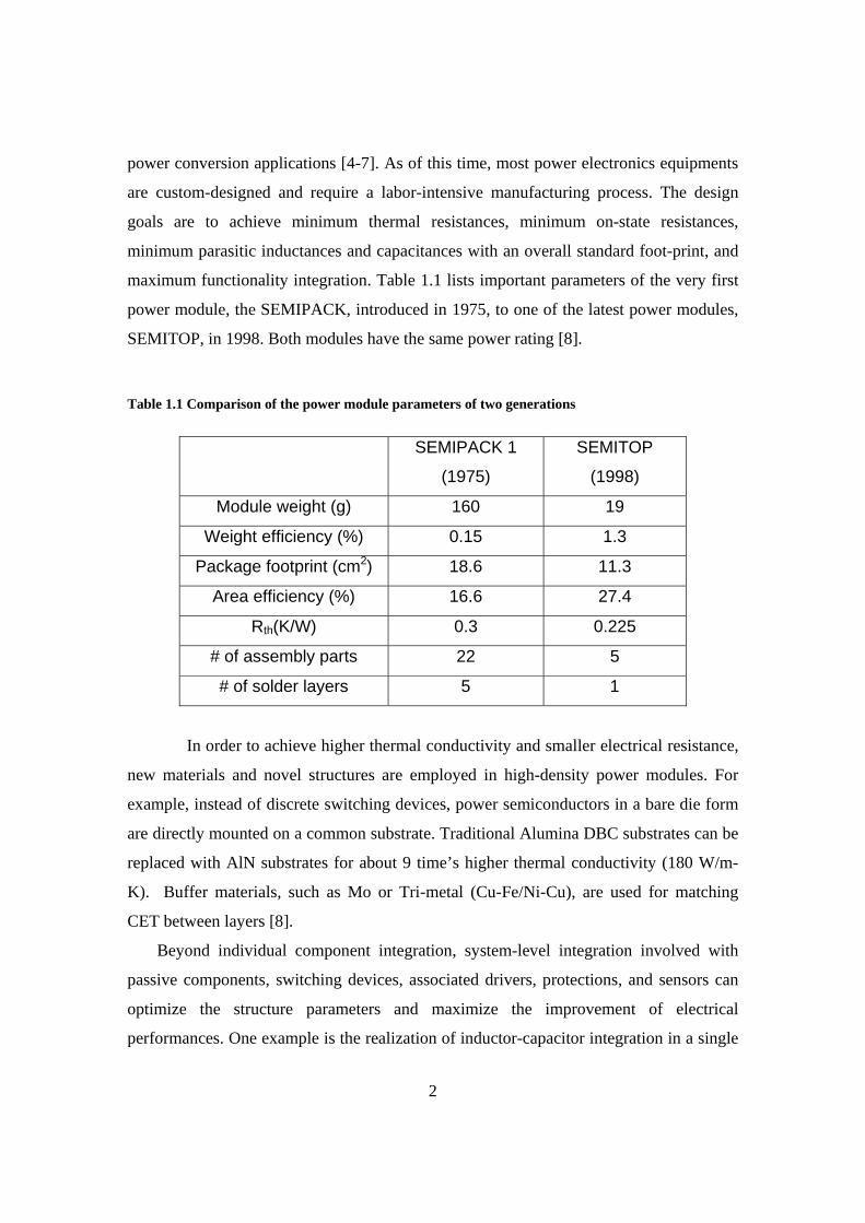
maximum functionality integration. Table 1.1 lists important parameters of the very first
power module, the SEMIPACK, introduced in 1975, to one of the latest power modules,
SEMITOP, in 1998. Both modules have the same power rating [8].
Table 1.1 Comparison of the power module parameters of two generations
SEMIPACK 1
(1975)
SEMITOP
(1998)
Module weight (g) 160 19
Weight efficiency (%) 0.15 1.3
Package footprint (cm2) 18.6 11.3
Area efficiency (%) 16.6 27.4
Rth(K/W) 0.3 0.225
# of assembly parts 22 5
# of solder layers 5 1
In order to achieve higher thermal conductivity and smaller electrical resistance,
new materials and novel structures are employed in high-density power modules. For
example, instead of discrete switching devices, power semiconductors in a bare die form
are directly mounted on a common substrate. Traditional Alumina DBC substrates can be
replaced with AlN substrates for about 9 time’s higher thermal conductivity (180 W/m-
K). Buffer materials, such as Mo or Tri-metal (Cu-Fe/Ni-Cu), are used for matching
CET between layers [8].
Beyond individual component integration, system-level integration involved with
passive components, switching devices, associated drivers, protections, and sensors can
optimize the structure parameters and maximize the improvement of electrical
performances. One example is the realization of inductor-capacitor integration in a single
3
module. As mentioned previously, the improvement of the power semiconductor devices
results in an increase of the circuit working frequency to megahertz or higher. As the
frequency increases, the structural effect of passive components becomes more and more
significant. The parasitic inductance of a capacitor in a low frequency can be ignored.
However, in a high frequency range, the capacitor may behave as an inductor due to this
parasitic effect. Although there have been many efforts to decreasing parasitic
components, the limitation of discrete passive components cannot be overcome. The
integration of discrete capacitive and inductive components into one electromagnetic
component has become a research topic in recent years. The study of generalized
inductor-capacitor (LC) components and the integrated inductor-capacitor-transformer
(LCT) modules used in converter systems are presented in [9-11]. As an alternative to a
discrete inductor and capacitor LC resonant circuit, the planar LC resonant module
demonstrates promising merits for power electronic applications, such as less parasitics,
compatible mass manufacturing process, and potentially smaller size. The details will be
discussed later.
An Embedded Power module is another example of system level integration
involved with switching devices, associated drivers, and protection circuits. The
Embedded Power module is built by mounting silicon chips in the openings of a ceramic
substrate followed by printing a polymer dielectric isolation layer and vapor-depositing
multilayer metallic thin films for the construction of a three-dimensional package. There
are three major parts in the structure: embedded power chip stage, electronics circuits,
and base substrate. The electronic circuits consist of gate drive, control, and protection
components. The base substrate provides electrical interconnection and the major thermal
path for power chips. It will be introduced in the next chapter.
Although most power electronics modules are essentially custom-designed
nowadays, system-level integration and novel functionality packaging technologies
provide the possibility of manufacturing the standardized highly integrated Power
Electronics Building Blocks (PEBBs) [12]. In low power applications, the very-large-
scale-integration (VLSI) technology has shown tremendous advantages on
standardization, volume reduction, manufacturability, and cost reduction. In high power
applications, the monolithic integration in power IC forms is not suitable. The PEBB
4
approach integrates switching devices, circuits, controls, sensors, and actuators into
standardized manufactured subassemblies and modules. By employing different PEBBs
as power electronics modules with different functions to form a particular system, it is
expected that the PEBB approach will have the same advantages for high power systems.
However, developing PEBB is more complicated than low power VLSI circuits. Issues
include high current carrying capability, monolithic integration of associated control,
protection and sensor circuits, interconnection technology, thermal management, and
passives integration. All these are multi-disciplinary issues involving electrical, material,
and mechanical knowledge.
The renovation of interconnection technology in high density power technology is
associated with the material, structure change, and higher system level integration trends.
Wire bond technology is still widely used as the electrical contact from semiconductor
die chips to terminals. There are alternative interconnection technologies such as BGA
(Ball Grid Array), pressure contact, and planar interconnection, etc., depending on the
applications. The details about interconnection technologies will be covered in the next
section.
1.2 Current interconnection technologies
In integrated power modules, interconnections not only need to provide good
electrical contact, but also need to provide a good thermal path and a good mechanical
performance. The requirements for interconnecting materials include high electrical
conductivity, high resistance to electro-migration, high thermal conductivity, low thermal
coefficient of expansion, high strength and ductility, less fatigue problem, and ease of
processing. The most widely used metal interconnections for power devices include wire
bonds, solder balls, and planar metallization. The features of each technology are
introduced as follows.
1.2.1 Wire bonding
Wire bonding is a chip-to-package interconnection technique where a fine metal wire
is attached between the I/O pads on a chip and its associated package pin. This
technology originated from AT&T’s bean lead bonding in the 1950s. In this technology,
5
a fine wire, typically a gold wire with 25µm thickness, is bonded using ultrasonic
bonding between the IC bond pad and the matching package or the substrate bond pad.
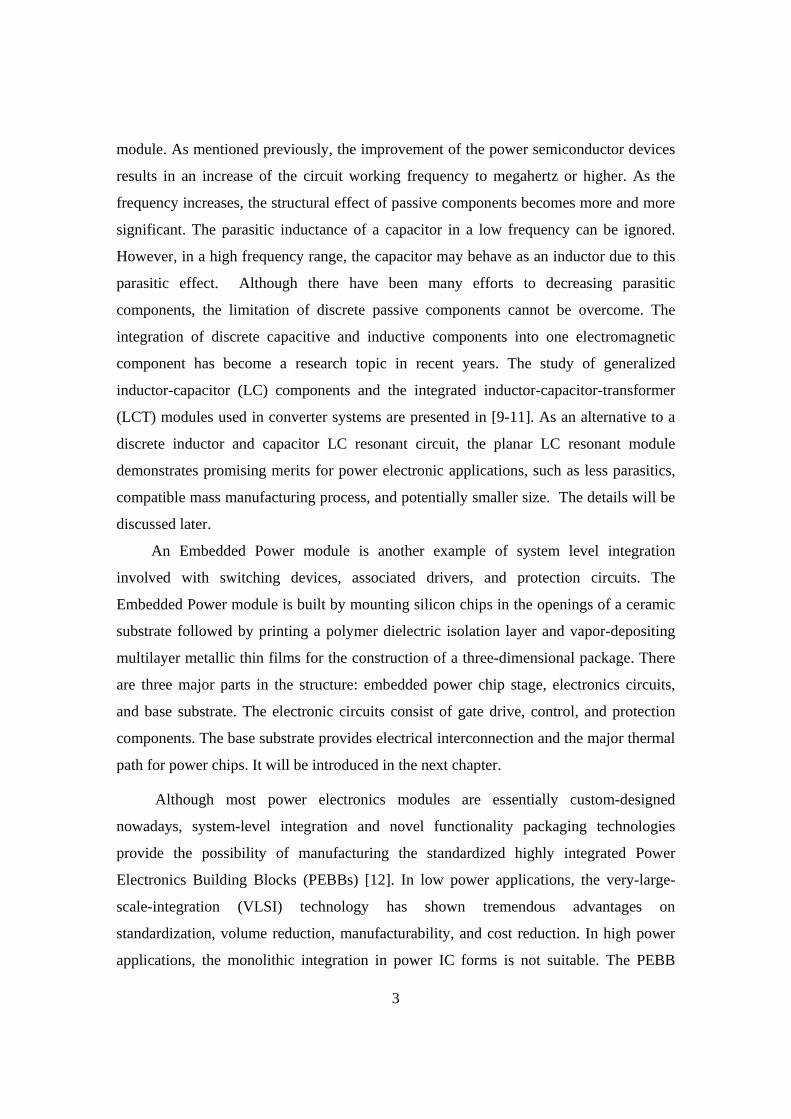
Wire bonding accounted for over 90% of all the chip-to package interconnections formed
in 1999 [13]. Fig. 1.2.1 shows a picture of wire bonded power modules [8].
Figure 1.2.1 Power modules using wire bonding interconnection
The advantages of wire bonding include the highly flexible chip-to-package
interconnection process, the high yield interconnection processing (40-1000ppm), the
easily programmed boning cycles, the very large industry infrastructure supporting the
technology, and the rapid advances in equipment, tools, and material technology. While it
is the most common method in use, it is perhaps the most limited for the future
development of high density, high-performance multi-chip modules [14]. The
disadvantages of the wire bonding interconnection include the slower interconnection
rates due to point-to-point processing of each wire bond, long chip-to package
interconnection lengths, degraded electrical performance, larger footprint required for
chip to package interconnection, and potential for wire sweep during encapsulation over
molding. A common failure in wire bonding plastic packages tends to occur due to
delamination of the encapsulant molding compound or die attach. It is followed by a
highly localized stress concentration in the wire bonds, causing fatigue failures in the
wires. A number of other failures are chip fracture, chip passivation cracking, chip
metallization corrosion, wire sweep, bond fracture and lift-off, interfacial delamination,
and package cracking.
6
1.2.2 Ball grid array
Current wire-bonding technology limits today’s smaller package sizes to pin counts
of 256 or less. With the ever-increasing demand for high density and high I/O count
packaging, area array packaging is rapidly becoming very popular in the industry. The
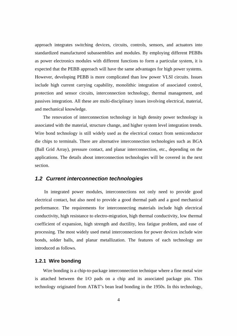
most common area array component is the ball grid array (BGA), which is shown in Fig.
1.2.2. The bottom side interconnection area can be extended over the size of the silicon
chip perimeter. The increased interconnection area enables an increase in the lead pitch,
which results in a more robust screen-printing process and causes less risk of short circuit
between leads. The solder balls used in the interconnection between the component and
the board provide a shorter electrical path, which therefore, has less parasitic inductance
and causes less degradation of the signal.
Figure 1.2.2 Schematic of a BGA module
The advantages of BGA over traditional packaging include higher interconnect
densities, better electrical performance due to a shorter distance between chip and solder
balls, better thermal performance by using thermal vias, reduced placement problems,
and reduced handling issues [15]. Hopefully, the many advantages of this interconnection
technology will also benefit power electronics. Currently, most of the commercial power
devices packaged by flip chip solder bumping are in the low to medium power ranges.
Requirements for the adoption of flip chip area array solder bumping in power electronics
packaging include high current handling capability, better thermal management, process
7
compatibility, and good insulation and understanding of the reliability of the solder
bumping interconnection.
One big drawback with a BGA component is the difficulty to inspect the formed
solder joints after assembly. X-ray method can inspect BGA components. However, it is
very difficult to judge the appearance of the solder joint. The inspection is very time-
consuming, as compared to using a microscope for standard surface mounted components.
Furthermore, the BGA technology is not compatible with the integrated power
technology used for further integration of power passives and power active devices.
1.2.3 Planar metallization interconnection
The fundamental approach to electronics power conversion has steadily moved
toward “high-frequency synthesis”, resulting in huge improvements in converter
performance, size, weight, and cost. However, as with many high-frequency power
conversion technologies, fundamental limits are being reached that will not be overcome
without a radical change in the power conversion strategy [16]. Integration technology is
essential to further decrease module size and increase power density. There are two main
categories for integration technology: structural integration and function integration.
Structural integration is used to make discrete devices and components in an
integrated process or in an integrated structure. Examples of such technologies are 3-D
integration modules, low temperature co-fired ceramics (LTCC), and embedded passives
for PCBs. In the power IC industry, the vertical interconnections are standardized and
commercially available for 3-D integration. It offers short interconnection paths and
makes mass production a possibility. As shown in Fig.1.2.3, the same concept can be
used for power module packaging technology. Instead of using wire bonds, the switching
devices can be interconnected by a planar metallization layer. The Embedded Power, to
be introduced later, is a good structural integration example of utilizing the planar
metallization to replace the wire bond and embedding passive components with
compatible processes.
8
Figure 1.2.3 Cross section schematic of a 3-D integration module
The use of embedded passive components for Printed Circuit Boards (PCB) is a very
promising integration technology. To integrate capacitors into a PCB, capacitive
materials can replace the insulation layers. The conductors on top and bottom of this
layer form the electrodes of the integrated capacitors. The capacitive layers can be used
to replace resonant capacitors, filters, decoupling and snubber capacitors, and timing
capacitors for controllers. Most of the layers exhibit a high breakdown voltage (1000V or
higher). At least two materials (Isola C-Lam, Roger RO3210) and their manufacturing
process for PCB are already commercially available. The cost can be moderate. The
integration of capacitors into PCB will become state of the art soon; however, very high
capacitive materials to replace electrolytic capacitors are far from being realized [17].
Functional integration manufactures an integrated device, which can present
combined electrical functions. Examples are integrated filters and inductor-capacitor-
transformer modules used in converter system. The integrated modules present the
desired function combinations of capacitors, inductors, and even transformers in certain
frequency ranges. The integration of passive components is a technology for highly
integrated electronic circuits, because they typically need more than 2/3 of the space of a
conventional circuit. This is especially necessary for applications that need an ultra-thin
building height such as thin, flat displays [17].
The combination of structural integration and functional integration has the
following advantages: a much more compact and thinner circuit, a compatible
9
manufacturing process for different kind of modules and circuits, a large potential for
cost reduction, a better reproducibility, a better reliability because the interconnections
are no longer mechanical fixings, a better EMI performances, better recyclables because
less materials are used, and a standardized layered structure.
The main feature of the structural and functional integration is the planar structure,
which therefore makes the interconnection layers planar. Unlike wire bonding or BGA
interconnections, which have to be processed individually for each terminal, planar
metallization enables a massive parallel processing for all modules. The planar
metallization process is also compatible with either active switching device connections,
which have silicon as the substrate, or passive device connections, which have ceramic as
the substrate. To evaluate the planar metallization interconnection, we need to consider
electrical performance, mechanical performance, and thermal performance. Compared
with wire bond, planar interconnections have shortened electrical paths and smaller
parasitic inductance, which is suitable for high frequency applications. As shown by the
comparison of the packages depicted in Fig. 1.2.1, Fig. 1.2.2 and Fig.1.2.3, the heat
generated by switching devices can be removed mainly from the bottom side of the
package for the wire bonding technology or the BGA package, while the planar top
surfaces enable the double-side cooling for better thermal management. Due to the large
area of contact between different material layers in planar metallization, the mismatch of
coefficient thermal expansion (CTE) will be an issue in 3-D packaging. The mechanical
behavior and performances of planar metallization in power electronics modules needs to
be investigated.
1.3 Applications of the planar interconnect technology
1.3.1 Embedded Power modules
In today’s power electronics modules, power semiconductor devices such as
MOSFETs and IGBTs are interconnected via wire bonds. These bonds are susceptible to
ringing due to the long interconnection path, which will cause higher stresses for
switching devices and larger EMI noise. Over the last few years, a planar interconnection
technique has been developed to enable the construction of 3-D integrated power
10
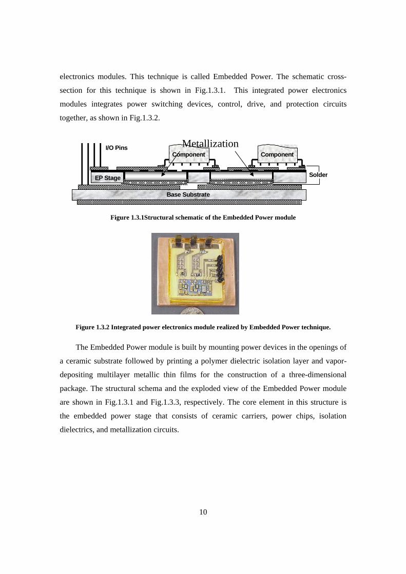
electronics modules. This technique is called Embedded Power. The schematic cross-
section for this technique is shown in Fig.1.3.1. This integrated power electronics
modules integrates power switching devices, control, drive, and protection circuits
together, as shown in Fig.1.3.2.
Component Component
Base Substrate
I/O Pins
Solder EP Stage
Figure 1.3.1Structural schematic of the Embedded Power module
Figure 1.3.2 Integrated power electronics module realized by Embedded Power technique.
The Embedded Power module is built by mounting power devices in the openings of
a ceramic substrate followed by printing a polymer dielectric isolation layer and vapor-
depositing multilayer metallic thin films for the construction of a three-dimensional
package. The structural schema and the exploded view of the Embedded Power module
are shown in Fig.1.3.1 and Fig.1.3.3, respectively. The core element in this structure is
the embedded power stage that consists of ceramic carriers, power chips, isolation
dielectrics, and metallization circuits.
Metallization
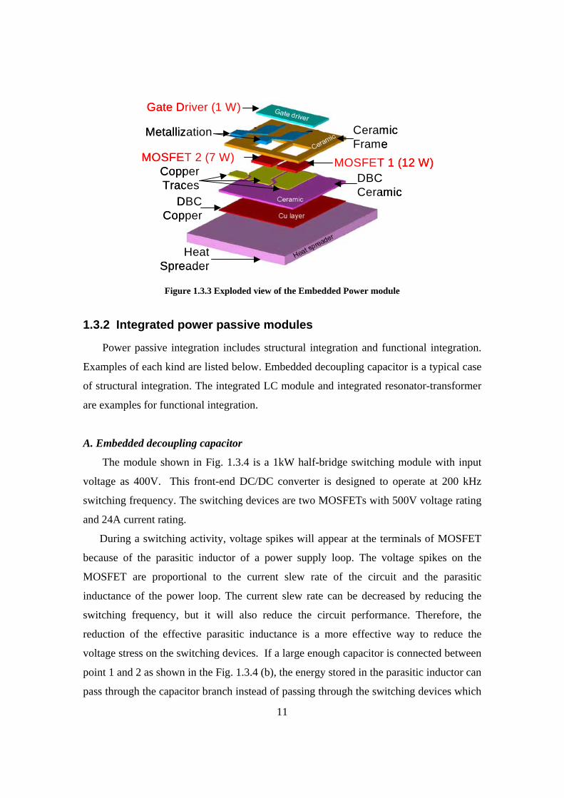
11
Heat Spreader
DBC Ceramic
DBC Copper
Copper Traces
MOSFET 1 (12 W)MOSFET 2 (7 W)
Ceramic Frame
Metallization
Gate Driver (1 W)
Heat Spreader
DBC Ceramic
DBC Copper
Copper Traces
MOSFET 1 (12 W)MOSFET 2 (7 W)
Ceramic Frame
Metallization
Gate Driver (1 W)
Figure 1.3.3 Exploded view of the Embedded Power module
1.3.2 Integrated power passive modules
Power passive integration includes structural integration and functional integration.
Examples of each kind are listed below. Embedded decoupling capacitor is a typical case
of structural integration. The integrated LC module and integrated resonator-transformer
are examples for functional integration.
A. Embedded decoupling capacitor
The module shown in Fig. 1.3.4 is a 1kW half-bridge switching module with input
voltage as 400V. This front-end DC/DC converter is designed to operate at 200 kHz
switching frequency. The switching devices are two MOSFETs with 500V voltage rating
and 24A current rating.
During a switching activity, voltage spikes will appear at the terminals of MOSFET
because of the parasitic inductor of a power supply loop. The voltage spikes on the
MOSFET are proportional to the current slew rate of the circuit and the parasitic
inductance of the power loop. The current slew rate can be decreased by reducing the
switching frequency, but it will also reduce the circuit performance. Therefore, the
reduction of the effective parasitic inductance is a more effective way to reduce the
voltage stress on the switching devices. If a large enough capacitor is connected between
point 1 and 2 as shown in the Fig. 1.3.4 (b), the energy stored in the parasitic inductor can
pass through the capacitor branch instead of passing through the switching devices which
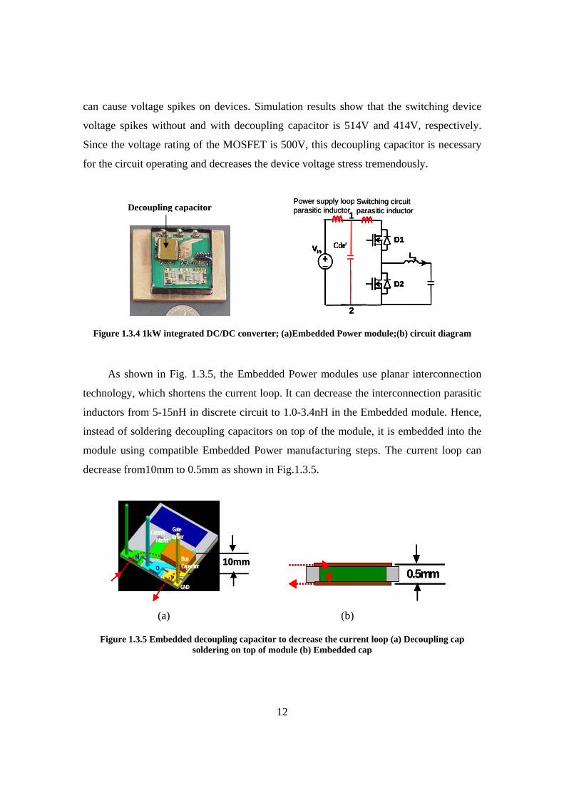
12
can cause voltage spikes on devices. Simulation results show that the switching device
voltage spikes without and with decoupling capacitor is 514V and 414V, respectively.
Since the voltage rating of the MOSFET is 500V, this decoupling capacitor is necessary
for the circuit operating and decreases the device voltage stress tremendously.
LoVin
Power supply loopparasitic inductor
Cde’D1
D2
LoVin
Cde’D1
D2
LoVin
Cde’D1
D2
1
2
Switching circuit parasitic inductor
LoVin
Power supply loopparasitic inductor
Cde’D1
D2
LoVin
Cde’D1
D2
LoVin
Cde’D1
D2
1
2
Switching circuit parasitic inductor
Figure 1.3.4 1kW integrated DC/DC converter; (a)Embedded Power module;(b) circuit diagram
As shown in Fig. 1.3.5, the Embedded Power modules use planar interconnection
technology, which shortens the current loop. It can decrease the interconnection parasitic
inductors from 5-15nH in discrete circuit to 1.0-3.4nH in the Embedded module. Hence,
instead of soldering decoupling capacitors on top of the module, it is embedded into the
module using compatible Embedded Power manufacturing steps. The current loop can
decrease from10mm to 0.5mm as shown in Fig.1.3.5.
P
NO
GND
Gate DriverCeramic
Bus Capacitor
Mosfet
P
NO
GND
Gate DriverCeramic
Bus Capacitor
Mosfet
10mmP
NO
GND
Gate DriverCeramic
Bus Capacitor
Mosfet
P
NO
GND
Gate DriverCeramic
Bus Capacitor
Mosfet
P
NO
GND
Gate DriverCeramic
Bus Capacitor
Mosfet
P
NO
GND
Gate DriverCeramic
Bus Capacitor
Mosfet
10mm
0.5mm0.5mm
(a) (b)
Figure 1.3.5 Embedded decoupling capacitor to decrease the current loop (a) Decoupling cap soldering on top of module (b) Embedded cap
Decoupling capacitor
13
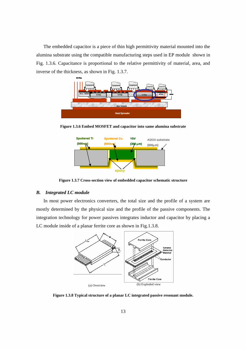
The embedded capacitor is a piece of thin high permittivity material mounted into the
alumina substrate using the compatible manufacturing steps used in EP module shown in
Fig. 1.3.6. Capacitance is proportional to the relative permittivity of material, area, and
inverse of the thickness, as shown in Fig. 1.3.7.
Heat Spreader
C-ChipS-ChipS-Chip
Component
I/O Pins
Solder
Component Component
Base Substrate
R-CoilStruc. Ceramic
ComponentComponent
Heat SpreaderHeat Spreader
C-ChipS-ChipS-Chip
Component
I/O Pins
Solder
Component Component
Base Substrate
R-CoilStruc. Ceramic
ComponentComponent
C-ChipS-ChipS-Chip
ComponentComponent
I/O Pins
Solder
ComponentComponent ComponentComponent
Base Substrate
R-CoilStruc. Ceramic
ComponentComponentComponentComponent
Figure 1.3.6 Embed MOSFET and capacitor into same alumina substrate
Al2O3 substrate
(600µm)
Sputtered Ti
(500nm)
Y5V
(300 µm)
Sputtered Cu
(500nm)
epoxy
Al2O3 substrate
(600µm)
Sputtered Ti
(500nm)
Y5V
(300 µm)
Sputtered Cu
(500nm)
epoxy
Figure 1.3.7 Cross-section view of embedded capacitor schematic structure
B. Integrated LC module
In most power electronics converters, the total size and the profile of a system are
mostly determined by the physical size and the profile of the passive components. The
integration technology for power passives integrates inductor and capacitor by placing a
LC module inside of a planar ferrite core as shown in Fig.1.3.8.
(a) Overview (b) Exploded view
Figure 1.3.8 Typical structure of a planar LC integrated passive resonant module.
14
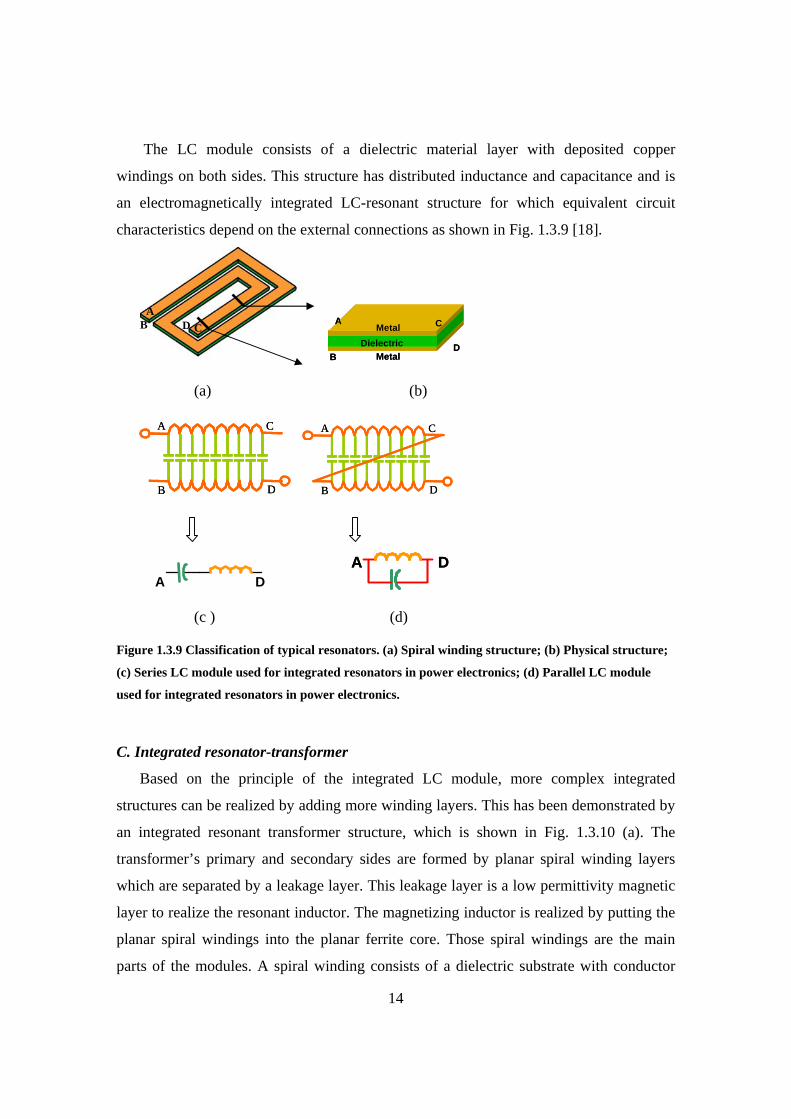
The LC module consists of a dielectric material layer with deposited copper
windings on both sides. This structure has distributed inductance and capacitance and is
an electromagnetically integrated LC-resonant structure for which equivalent circuit
characteristics depend on the external connections as shown in Fig. 1.3.9 [18].
AB CD
AB CD
Dielectric
Metal
Metal
A C
BDDielectric
Metal
Metal
A C
BD
(a) (b)
A
B
C
D
A
B
C
D
A
B
C
D
A
B
C
D
A D
A DA D
(c ) (d)
Figure 1.3.9 Classification of typical resonators. (a) Spiral winding structure; (b) Physical structure;
(c) Series LC module used for integrated resonators in power electronics; (d) Parallel LC module
used for integrated resonators in power electronics.
C. Integrated resonator-transformer
Based on the principle of the integrated LC module, more complex integrated
structures can be realized by adding more winding layers. This has been demonstrated by
an integrated resonant transformer structure, which is shown in Fig. 1.3.10 (a). The
transformer’s primary and secondary sides are formed by planar spiral winding layers
which are separated by a leakage layer. This leakage layer is a low permittivity magnetic
layer to realize the resonant inductor. The magnetizing inductor is realized by putting the
planar spiral windings into the planar ferrite core. Those spiral windings are the main
parts of the modules. A spiral winding consists of a dielectric substrate with conductor
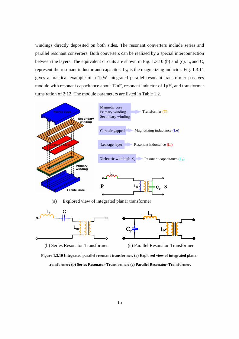
15
windings directly deposited on both sides. The resonant converters include series and
parallel resonant converters. Both converters can be realized by a special interconnection
between the layers. The equivalent circuits are shown in Fig. 1.3.10 (b) and (c). Lr and Cr
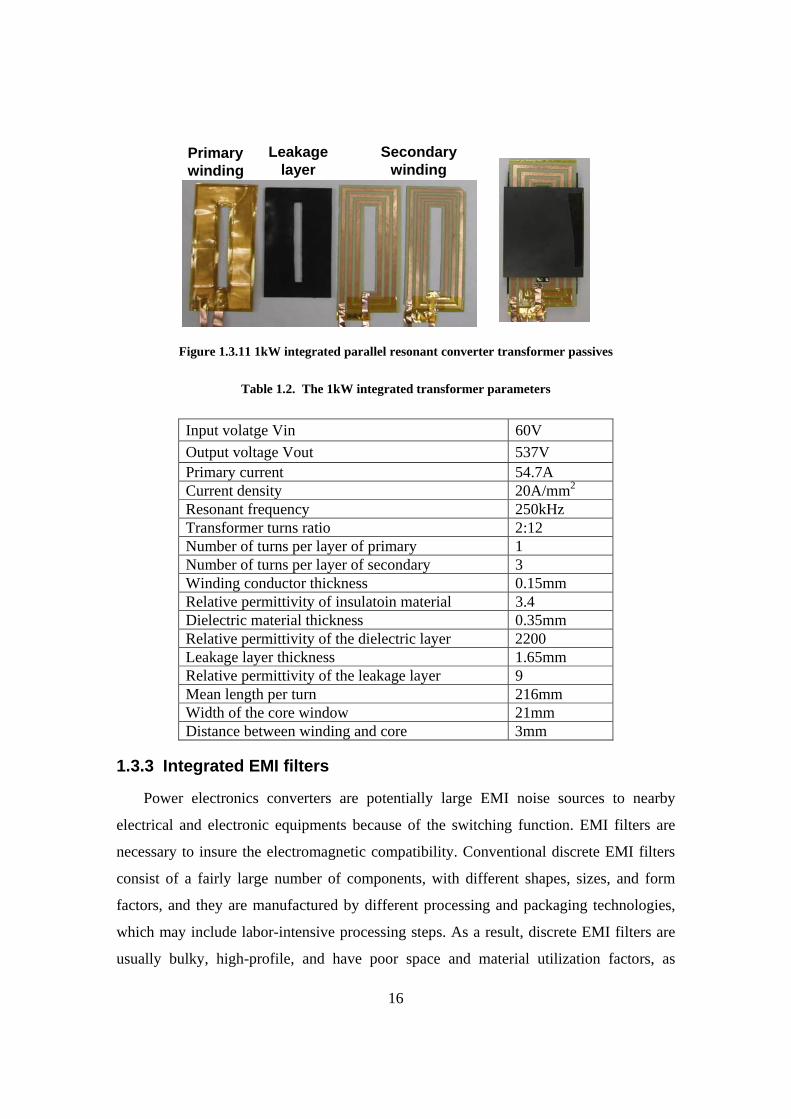
represent the resonant inductor and capacitor. LM is the magnetizing inductor. Fig. 1.3.11
gives a practical example of a 1kW integrated parallel resonant transformer passives
module with resonant capacitance about 12nF, resonant inductor of 1µH, and transformer
turns ration of 2:12. The module parameters are listed in Table 1.2.
Magnetic corePrimary windingSecondary winding
Transformer (T)
Core air gapped Magnetizing inductance (LM)
Leakage layer Resonant inductance (Lr)
Dielectric with high rε Resonant capacitance (Cp)
S
Lr
CpP LM
Lr
CpP LM
(a) Explored view of integrated planar transformer
Lr
Cr LM
Lr
Cr LM
(b) Series Resonator-Transformer (c) Parallel Resonator-Transformer
Figure 1.3.10 Integrated parallel resonant transformer. (a) Explored view of integrated planar
transformer; (b) Series Resonator-Transformer; (c) Parallel Resonator-Transformer.
L
r C r
L m
16
Primary winding
Leakage layer
Secondary winding
Figure 1.3.11 1kW integrated parallel resonant converter transformer passives
Table 1.2. The 1kW integrated transformer parameters
Input volatge Vin 60V Output voltage Vout 537V Primary current 54.7A Current density 20A/mm2
Resonant frequency 250kHz Transformer turns ratio 2:12 Number of turns per layer of primary 1 Number of turns per layer of secondary 3 Winding conductor thickness 0.15mm Relative permittivity of insulatoin material 3.4 Dielectric material thickness 0.35mm Relative permittivity of the dielectric layer 2200 Leakage layer thickness 1.65mm Relative permittivity of the leakage layer 9 Mean length per turn 216mm Width of the core window 21mm Distance between winding and core 3mm
1.3.3 Integrated EMI filters
Power electronics converters are potentially large EMI noise sources to nearby
electrical and electronic equipments because of the switching function. EMI filters are
necessary to insure the electromagnetic compatibility. Conventional discrete EMI filters
consist of a fairly large number of components, with different shapes, sizes, and form
factors, and they are manufactured by different processing and packaging technologies,
which may include labor-intensive processing steps. As a result, discrete EMI filters are
usually bulky, high-profile, and have poor space and material utilization factors, as
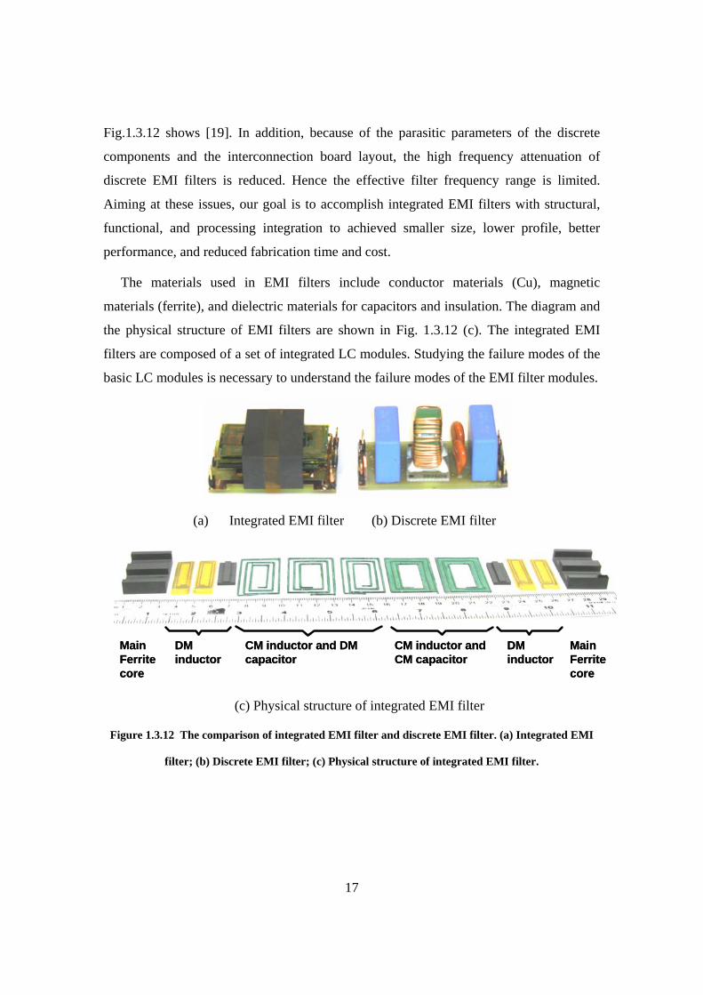
17
Fig.1.3.12 shows [19]. In addition, because of the parasitic parameters of the discrete
components and the interconnection board layout, the high frequency attenuation of
discrete EMI filters is reduced. Hence the effective filter frequency range is limited.
Aiming at these issues, our goal is to accomplish integrated EMI filters with structural,
functional, and processing integration to achieved smaller size, lower profile, better
performance, and reduced fabrication time and cost.
The materials used in EMI filters include conductor materials (Cu), magnetic
materials (ferrite), and dielectric materials for capacitors and insulation. The diagram and
the physical structure of EMI filters are shown in Fig. 1.3.12 (c). The integrated EMI
filters are composed of a set of integrated LC modules. Studying the failure modes of the
basic LC modules is necessary to understand the failure modes of the EMI filter modules.
(a) Integrated EMI filter (b) Discrete EMI filter
Main Ferrite core
DM inductor
CM inductor and DM capacitor
CM inductor and CM capacitor
DM inductor
Main Ferrite core
Main Ferrite core
DM inductor
CM inductor and DM capacitor
CM inductor and CM capacitor
DM inductor
Main Ferrite core
(c) Physical structure of integrated EMI filter
Figure 1.3.12 The comparison of integrated EMI filter and discrete EMI filter. (a) Integrated EMI
filter; (b) Discrete EMI filter; (c) Physical structure of integrated EMI filter.
18
1.4 Aim of this study
Over the past several decades, extensive research into the drivers of failure
mechanisms in integrated power modules has led to an understanding of failure
mechanisms, chiefly centered on wire bond and solder layer failures. The lifetime
estimation in planar metallization power package is different from ball grid array or chip-
scale packages because of the different physical interconnection dimensions and different
failure modes. For example, for the case of solder-joint fatigue in packages with tens of
hundreds of I/O connections, the failure of a single I/O may constitute the failure of the
package. Furthermore, since the physical dimensions of each connection are tens of
micrometers, the estimation of failure initiation often corresponds closely to the end of
life, owing to the immediate impact of failure initiation on joint integrity. In contrast,
since power connections are often orders of magnitude larger (tens of millimeters), there
is a greater tolerance to such defects. Instead, the major effects are manifested as a
lowered thermal resistance, which directly affects the electrical performance of the device
systems [20].
As to the novel planar integrated technology used in power electronics, new material
combination and new structures are used. The failure modes for the integrated power
modules based on the thick copper deposition on brittle materials and high current
working conditions of the power modules are not fully understood.
1.4.1 Summary of related research
As introduced previously, the planar interconnection is widely used in the IC
industry. By adopting this technology in power applications, unique features are
introduced: (1) the thickness of metal deposition is in the range of 100µm to conduct high
current in power circuits, which is much thicker than the IC application; (2) the copper
deposition on brittle materials is critical for circuit operation. It is also the most probable
failure spots. The design, manufacture, optimization, and testing of the IPEMs has been
developed and well documented over the last few years. Up to this date, the failure
mechanism research of conventional integrated power modules has led to the
understanding of failures centered on wire bond or solder layer. However, the IPEM
19
reliability and failure modes investigation based on the metallization on brittle substrates
for high current operations is still lacking.
Some research on the DBC copper-ceramic interface failure of power electronics
modules has been done by Johannes Juul Mikkelsen and his group [21]. The DBC
substrates used in the experiments are production samples for a 2kW integrated power
converter. The substrates are standard-grade 96% Al2O3 ceramic, 0.635mm thick. The
copper layers are 0.3mm thick. Half of the samples are soldered to a 4mm copper base.
The other half of the substrates are left free. The results show that soldering conditions
will significantly change the failure development. The failure mode is the same. In both
cases fracture goes down from the edge of the DBC copper layer. However, in the
mounted condition, the failure only occurs near the edge of the DBC and the cracked area
is significantly smaller than that in the free condition.
The research group led by Prof. Mike Shaw studied the strength distribution of the
ceramic materials properties and measured the fracture toughness of the metal-ceramic
interfaces [22]. Five types of brittle ceramic materials used in integrated passives and
integrated EMI filters are experimentally characterized for their strength distributions and
fracture toughness. The failure and reliability criteria for brittle materials are governed by
both the applied stress and a length-scale parameter, such as the defect size or the layer
thickness. These dual requirements represent a fundamental distinction compared to most
ductile materials, where only a stress or strain-based parameter is required to reliably
predict failure. The interfacial delamination or peeling often occurs at levels of stress or
temperature well below those needed to induce fracture or yield of the materials on either
side of the interface. This can result either from an adhesive joint with insufficient
fracture toughness or the presence of a defect population with unacceptably large
dimensions. The strength distributions of the brittle constituents were measured in biaxial
loading. The controlled cracks produced by the Vicers technique have been applied to
previous investigations to explore the fracture toughness of the interface in ceramic/metal
multilayer. Delamination along the interface is visible, indicating a lower critical strain
energy release rate than that of the ceramic. Although preliminary, this technique is
invaluable in rapid assessment of the adhesion of such interfaces.
20
1.4.2 Research work covered in this study
In this study, the integrated power modules are manufactured and their lifetime is
tested. It is expected that most of the mechanical failures are caused by the delamination
of the metal layer from the substrate. Poor interface adhesion, intrinsic residual stress,
and thermally induced mechanical stresses are possible contributing factors causing
failure of these modules. These factors are studied respectively in embedded power
modules and integrated passive modules.
In Chapter 2, the manufacturing processes of different kinds of integrated power
modules are introduced first. Metallization on brittle materials is one of the major
features of integrated power modules. The interface conditions for different structures are
reviewed from the material science point of view and the research is the results of
extensive thin film studies.
Residual stress and thermal mechanical stress are two major stresses in the system
which can cause failures. Chapter 3 covers the residual stress background knowledge and
introduces an experimental method to measure and calculate the residual stress
introduced by the planar integration process. Since directly measuring the residual stress
in a complicated structure is a very difficult task, a simplified copper-glass structure is
chosen as the experiment samples. The deposition processes are the same as those in the
integrated modules. The curvature of the glass slide is measured by a surface profile
system and the stress is calculated based on this curvature.
Chapter 4 investigates the thermo-mechanical stresses in the integrated power
modules. There are two approaches to analyze the thermal stresses in a layered structure.
The layered structure can be modeled as beams. The thermal stress can be calculated
using the force equilibrium equations. With simplified assumptions, the model can
predict the thermal stresses in layered structures. This approach can provide easy-to-use
expressions. The second approach is to use the finite element analysis to analyze the
stresses. Although it cannot provide a simple expression, like the previous method does,
finite element analysis is the more effective tool for complicated structures, where the
simplified assumptions that are necessary to make the expressions manageable may lead
to large errors. In chapter 4, both theoretical analysis and software simulation are used to
study the thermal stress in a simplified bi-layer structure and the results are compared.
21
The matching results verify that finite element analysis is an effective tool to study the
thermal stress in a complicated structure. A multi-layered module is then simulated and
the stress distribution is presented.
In order to verify the stress analysis results, lifetime tests of the integrated modules
are designed and carried out in chapter 5. The manufacturing process used to prepare the
test samples is identical to that of the Embedded Power modules. According to literature,
the thin films under tensile and compressive stresses have different failure modes. In
order to separate the driving forces for different failure modes, two temperature profiles
are used. Failed sample investigation indicates the major failure modes for different stress
conditions. Further understanding of those failure mechanisms enables the engineering of
the failure modes for safe electrical operations of IPEM modules and helps to enhance the
reliability of system-level operations. It is the basis for improving the design and for
optimizing the process parameters to achieve a high resistance to the failure. It is also
helpful to establish the methodology for failure prediction based on the understanding of
the recognized failure modes.
Chapter 6 covers the optimization design in simplified structure. Optimization of
geometry and material parameters such as thickness ratio, length ratio, critical size,
adhesion material and substrate materials are discussed based on the modeling results.
This provides the guidelines for practical IPEM design.
Chapter 7 is the summary and discussion of future work.

22
Chapter 2: Metal Films on Brittle Substrates in IPEMs
2.1 Fabrication processes of integrated modules
2.1.1 Integrated active modules (Embedded Power)
As shown in Fig. 2.1.1, a fully integrated power module includes three main layers:
base substrate, Embedded Power stage, and necessary components soldered on top of the
power stage. The base plate usually employs a direct-bonded-copper (DBC) ceramic
substrate. It is composed of a 500-625 µm-thick Alumina ceramic and two 200-250 µm-
thick copper on both sides. The vender is Curamik. The top copper layer of the DBC is
etched into certain patterns and is soldered into MOSFET chip drain electrodes. The
bottom copper layer of DBC is in direct contact with a heat spreader for thermal
management. The components soldered on top of the power stage are capacitors, resistors,
and driver chips. They are all surface mounted components. The solder paste used for the
base plate and components soldering is the no clean low residue Sn63Pb37 from
SolderPlusTM. The embedded power stage is the most important part. The fabrication
processes are shown in Fig.2.1.2. The typical packaging materials, structure parameters,
and vendor information are all listed in Table 2.1.
The power stage fabrication starts with an alumina ceramic working as a holding
frame. The ceramic is 96% alumina as-fired ceramic with a thickness of 500-625µm and
a size of 2 inches square (or 3 inches square depending on applications). The vender is
Valley Design®. The openings that hold the MOSFET chips are cut on the ceramic frame
by the laser cutting machine, which is shown in Fig. 2.1.2 (a).
The MOSFET chips are mounted in these openings with an adhesive epoxy
surrounding the edges. The epoxy is Master Bond’s EP3HT. After curing at 150°C for
about 7 minutes, the epoxy is hardened and provides good mechanical support for silicon
chips. A liquid photoimageable solder mask system ENTHONE®DSR-3241 A&B is then
spin coated on the top. After exposing it under UV light for about 8-10 minutes, the
sample is washed by the liquid developer concentrate D-4000 from DUPOND Electronic
Chemicals. The dielectric layer has the opening holes where the Al pad pattern of the
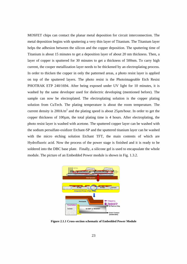
23
MOSFET chips can contact the planar metal deposition for circuit interconnection. The
metal deposition begins with sputtering a very thin layer of Titanium. The Titanium layer
helps the adhesion between the silicon and the copper deposition. The sputtering time of
Titanium is about 15 minutes to get a deposition layer of about 20 nm thickness. Then, a
layer of copper is sputtered for 30 minutes to get a thickness of 500nm. To carry high
current, the cooper metallization layer needs to be thickened by an electroplating process.
In order to thicken the copper in only the patterned areas, a photo resist layer is applied
on top of the sputtered layers. The photo resist is the Photoimageable Etch Resist
PHOTRAK ETP 240/1694. After being exposed under UV light for 10 minutes, it is
washed by the same developer used for dielectric developing (mentioned before). The
sample can now be electroplated. The electroplating solution is the copper plating
solution from CuTech. The plating temperature is about the room temperature. The
current density is 200A/m2 and the plating speed is about 25µm/hour. In order to get the
copper thickness of 100µm, the total plating time is 4 hours. After electroplating, the
photo resist layer is washed with acetone. The sputtered copper layer can be washed with
the sodium persulfate-oxidizer Etchant-SP and the sputtered titanium layer can be washed
with the micro etching solution Etchant TFT, the main contents of which are
Hydrofluoric acid. Now the process of the power stage is finished and it is ready to be
soldered into the DBC base plate. Finally, a silicone gel is used to encapsulate the whole
module. The picture of an Embedded Power module is shown in Fig. 1.3.2.
C o m p o n e n t C o m p o n e n t
B a s e S u b s tr a te
I/O P in s
S o ld e rE P S ta g e
Heat Spreader
Si chipSi chip Ceramic
Integrated Power Chips Stage
Al Pad on Chip
Drain Contact(Solderable)
Si IGBT or MOSFET Chip
Sputtered TiSputtered CuPlated Cu Polyimide
Ceramic
Passivation Eposxy
Figure 2.1.1 Cross-section schematic of Embedded Power Module
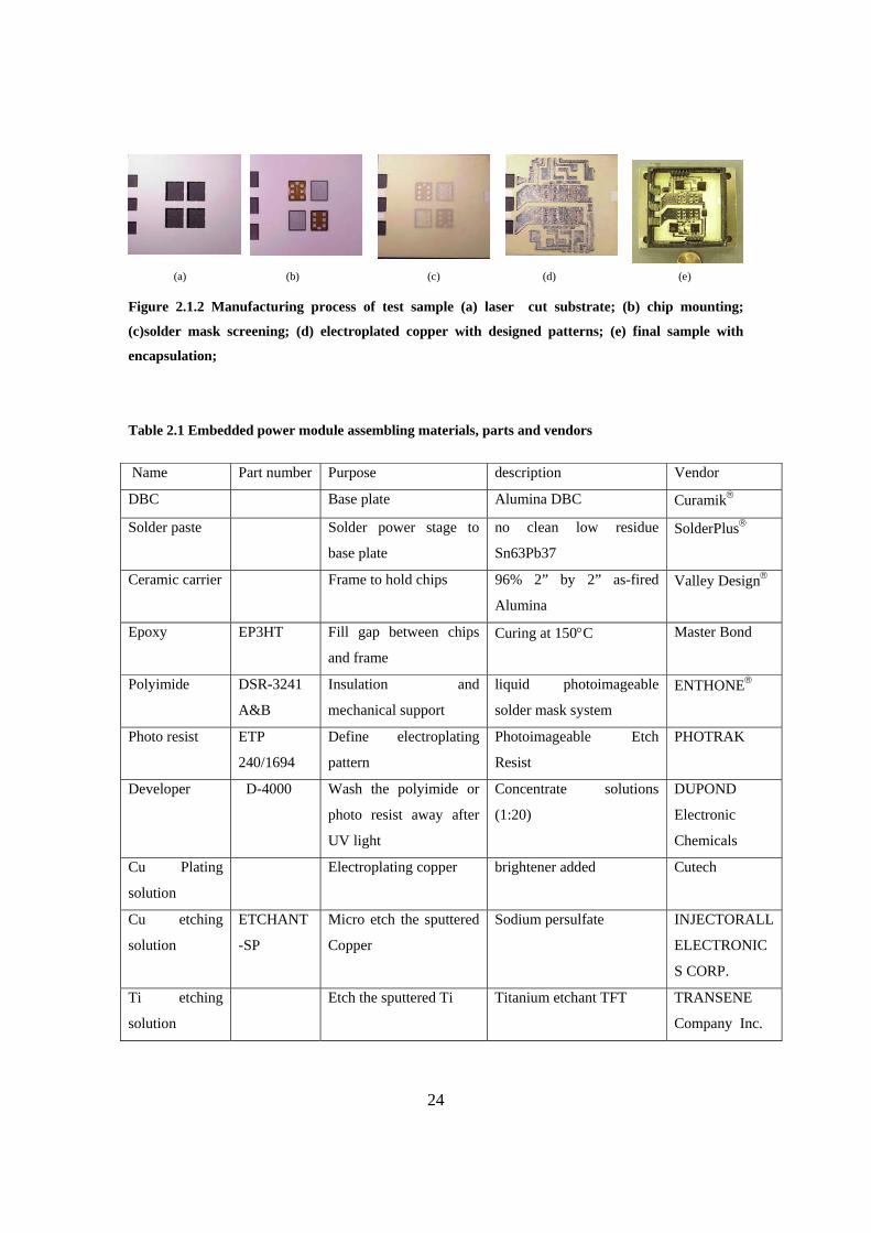
24
(a) (b) (c) (d) (e)
Figure 2.1.2 Manufacturing process of test sample (a) laser cut substrate; (b) chip mounting;
(c)solder mask screening; (d) electroplated copper with designed patterns; (e) final sample with
encapsulation;
Table 2.1 Embedded power module assembling materials, parts and vendors
Name Part number Purpose description Vendor
DBC Base plate Alumina DBC Curamik®
Solder paste Solder power stage to
base plate
no clean low residue
Sn63Pb37
SolderPlus®
Ceramic carrier Frame to hold chips 96% 2” by 2” as-fired
Alumina
Valley Design®
Epoxy EP3HT Fill gap between chips
and frame
Curing at 150°C Master Bond
Polyimide DSR-3241
A&B
Insulation and
mechanical support
liquid photoimageable
solder mask system
ENTHONE®
Photo resist ETP
240/1694
Define electroplating
pattern
Photoimageable Etch
Resist
PHOTRAK
Developer D-4000 Wash the polyimide or
photo resist away after
UV light
Concentrate solutions
(1:20)
DUPOND
Electronic
Chemicals
Cu Plating
solution
Electroplating copper brightener added Cutech
Cu etching
solution
ETCHANT
-SP
Micro etch the sputtered
Copper
Sodium persulfate INJECTORALL
ELECTRONIC
S CORP.
Ti etching
solution
Etch the sputtered Ti Titanium etchant TFT TRANSENE
Company Inc.
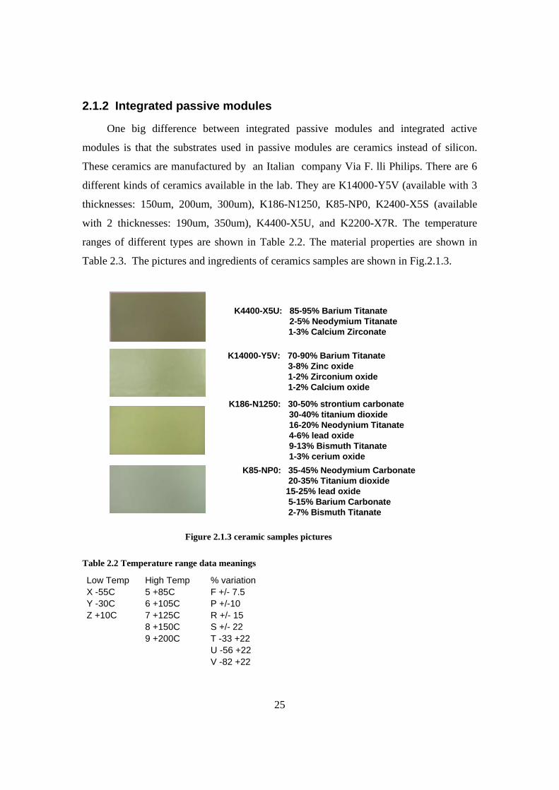
25
2.1.2 Integrated passive modules
One big difference between integrated passive modules and integrated active
modules is that the substrates used in passive modules are ceramics instead of silicon.
These ceramics are manufactured by an Italian company Via F. lli Philips. There are 6
different kinds of ceramics available in the lab. They are K14000-Y5V (available with 3
thicknesses: 150um, 200um, 300um), K186-N1250, K85-NP0, K2400-X5S (available
with 2 thicknesses: 190um, 350um), K4400-X5U, and K2200-X7R. The temperature
ranges of different types are shown in Table 2.2. The material properties are shown in
Table 2.3. The pictures and ingredients of ceramics samples are shown in Fig.2.1.3.
K4400-X5U: 85-95% Barium Titanate2-5% Neodymium Titanate1-3% Calcium Zirconate
K14000-Y5V: 70-90% Barium Titanate3-8% Zinc oxide1-2% Zirconium oxide1-2% Calcium oxide
K186-N1250: 30-50% strontium carbonate30-40% titanium dioxide16-20% Neodynium Titanate4-6% lead oxide9-13% Bismuth Titanate1-3% cerium oxide
K85-NP0: 35-45% Neodymium Carbonate20-35% Titanium dioxide15-25% lead oxide5-15% Barium Carbonate 2-7% Bismuth Titanate
Figure 2.1.3 ceramic samples pictures
Table 2.2 Temperature range data meanings
Low Temp High Temp % variation X -55C 5 +85C F +/- 7.5 Y -30C 6 +105C P +/-10 Z +10C 7 +125C R +/- 15 8 +150C S +/- 22 9 +200C T -33 +22 U -56 +22 V -82 +22
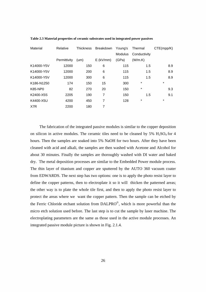
26
Table 2.3 Material properties of ceramic substrates used in integrated power passives
Material Relative Thickness Breakdown Young's Thermal CTE(mpp/K)
Permittivity (um) E (kV/mm)
Modulus
(GPa)
Conductivity
(W/m.K)
K14000-Y5V 12000 150 6 115 1.5 8.9
K14000-Y5V 12000 200 6 115 1.5 8.9
K14000-Y5V 12000 300 6 115 1.5 8.9
K186-N1250 174 150 15 300 * *
K85-NP0 82 270 20 150 * 9.3
K2400-X5S 2205 190 7 150 1.5 9.1
K4400-X5U 4200 450 7 128 * *
X7R 2200 180 7
The fabrication of the integrated passive modules is similar to the copper deposition
on silicon in active modules. The ceramic tiles need to be cleaned by 5% H2SO4 for 4
hours. Then the samples are soaked into 5% NaOH for two hours. After they have been
cleaned with acid and alkali, the samples are then washed with Acetone and Alcohol for
about 30 minutes. Finally the samples are thoroughly washed with DI water and baked
dry. The metal deposition processes are similar to the Embedded Power module process.
The thin layer of titanium and copper are sputtered by the AUTO 360 vacuum coater
from EDWARDS. The next step has two options: one is to apply the photo resist layer to
define the copper patterns, then to electroplate it so it will thicken the patterned areas;
the other way is to plate the whole tile first, and then to apply the photo resist layer to
protect the areas where we want the copper pattern. Then the sample can be etched by
the Ferric Chloride etchant solution from DALPRO®, which is more powerful than the
micro etch solution used before. The last step is to cut the sample by laser machine. The
electroplating parameters are the same as those used in the active module processes. An
integrated passive module picture is shown in Fig. 2.1.4.
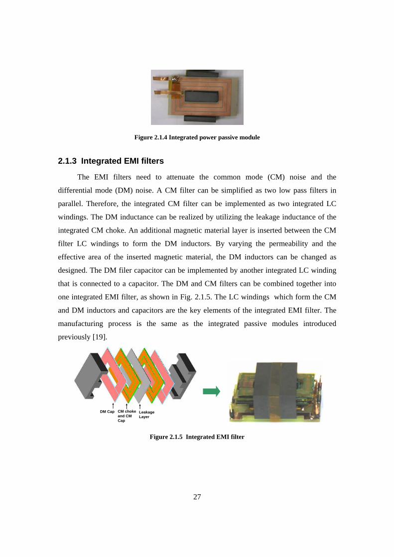
27
Figure 2.1.4 Integrated power passive module
2.1.3 Integrated EMI filters
The EMI filters need to attenuate the common mode (CM) noise and the
differential mode (DM) noise. A CM filter can be simplified as two low pass filters in
parallel. Therefore, the integrated CM filter can be implemented as two integrated LC
windings. The DM inductance can be realized by utilizing the leakage inductance of the
integrated CM choke. An additional magnetic material layer is inserted between the CM
filter LC windings to form the DM inductors. By varying the permeability and the
effective area of the inserted magnetic material, the DM inductors can be changed as
designed. The DM filer capacitor can be implemented by another integrated LC winding
that is connected to a capacitor. The DM and CM filters can be combined together into
one integrated EMI filter, as shown in Fig. 2.1.5. The LC windings which form the CM
and DM inductors and capacitors are the key elements of the integrated EMI filter. The
manufacturing process is the same as the integrated passive modules introduced
previously [19].
Leakage Layer
DM Cap CM choke and CM Cap
Figure 2.1.5 Integrated EMI filter
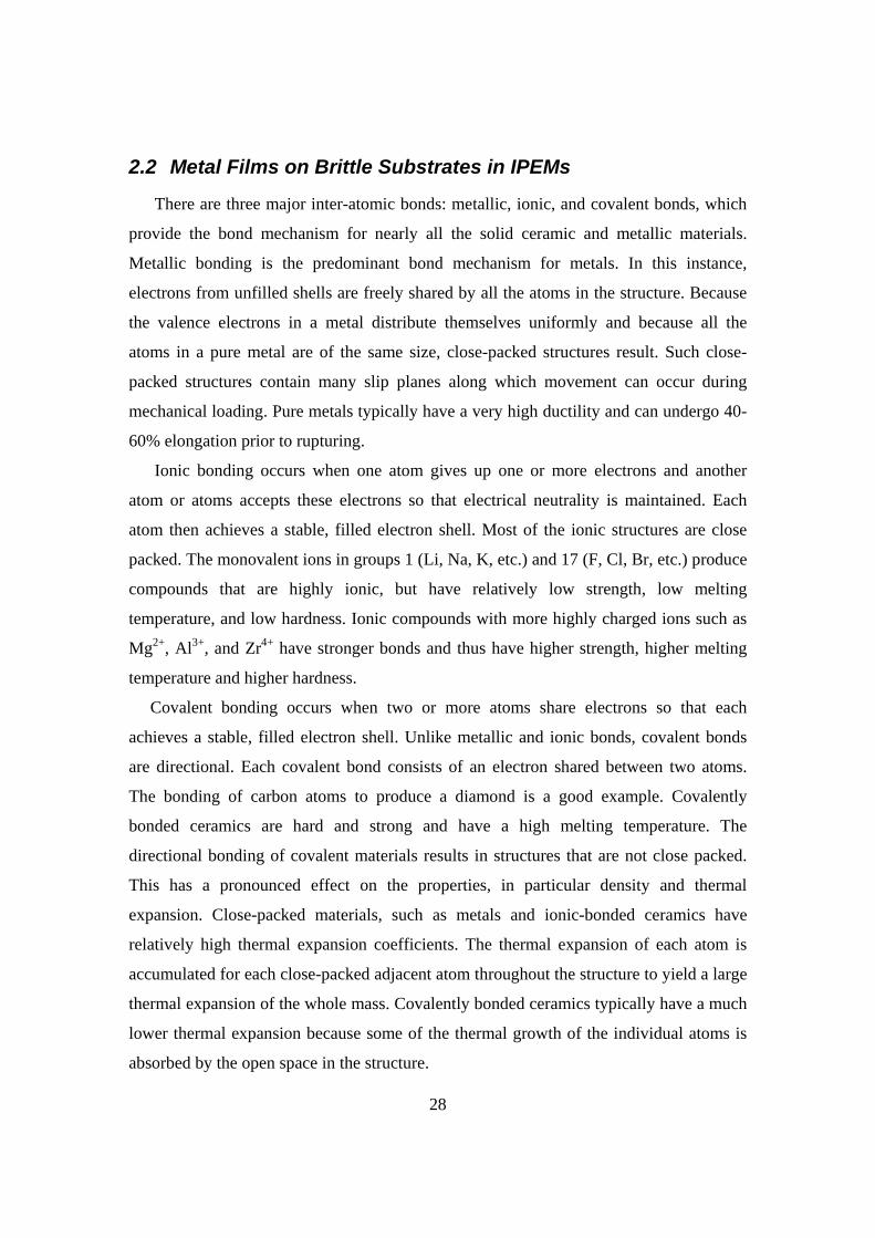
28
2.2 Metal Films on Brittle Substrates in IPEMs
There are three major inter-atomic bonds: metallic, ionic, and covalent bonds, which
provide the bond mechanism for nearly all the solid ceramic and metallic materials.
Metallic bonding is the predominant bond mechanism for metals. In this instance,
electrons from unfilled shells are freely shared by all the atoms in the structure. Because
the valence electrons in a metal distribute themselves uniformly and because all the
atoms in a pure metal are of the same size, close-packed structures result. Such close-
packed structures contain many slip planes along which movement can occur during
mechanical loading. Pure metals typically have a very high ductility and can undergo 40-
60% elongation prior to rupturing.
Ionic bonding occurs when one atom gives up one or more electrons and another
atom or atoms accepts these electrons so that electrical neutrality is maintained. Each
atom then achieves a stable, filled electron shell. Most of the ionic structures are close
packed. The monovalent ions in groups 1 (Li, Na, K, etc.) and 17 (F, Cl, Br, etc.) produce
compounds that are highly ionic, but have relatively low strength, low melting
temperature, and low hardness. Ionic compounds with more highly charged ions such as
Mg2+, Al3+, and Zr4+ have stronger bonds and thus have higher strength, higher melting
temperature and higher hardness.
Covalent bonding occurs when two or more atoms share electrons so that each
achieves a stable, filled electron shell. Unlike metallic and ionic bonds, covalent bonds
are directional. Each covalent bond consists of an electron shared between two atoms.
The bonding of carbon atoms to produce a diamond is a good example. Covalently
bonded ceramics are hard and strong and have a high melting temperature. The
directional bonding of covalent materials results in structures that are not close packed.
This has a pronounced effect on the properties, in particular density and thermal
expansion. Close-packed materials, such as metals and ionic-bonded ceramics have
relatively high thermal expansion coefficients. The thermal expansion of each atom is
accumulated for each close-packed adjacent atom throughout the structure to yield a large
thermal expansion of the whole mass. Covalently bonded ceramics typically have a much
lower thermal expansion because some of the thermal growth of the individual atoms is
absorbed by the open space in the structure.
29
Many ceramics materials have a combination of ionic and covalent bonding. However,
other weaker secondary bond mechanisms also occur, which can have major effects on
the properties of some ceramic materials. These secondary bonds are grouped together
under the name Van der Waals forces, which include dispersion, molecular polarization
and hydrogen bonding. Van der Waal forces are very important in layer structures such as
clays, micas, graphite, and hexagonal boron nitride. All of these ceramic materials have
strong primary bonding within their layers but depend on van der Waals-type bonds to
hold their layers together. Highly anisotropic properties result [23].
From the mechanical standpoint, brittle materials can be defined as those materials
which adhere strictly to Hook’s law of behavior. Ceramics materials (mostly covalent or
ionic-bonded) have complicated crystal structures involving two or three kinds of atoms.
Therefore, it is hard to have slip systems present in them. For brittle materials, the cracks
in the material create localized stress concentration fields. These stress fields cause the
propagation of cracks, thus producing brittle fractures. Brittle materials are materials
whose failure is primarily decided by the presence of flaws or cracks. In ductile materials,
cracks may be present, but the resulting stress concentrations are relieved by plastic
deformation, which prevents brittle fracture [24].
The flaw from which the cracking originated is often the primary focus of attention,
particularly if that failure has occurred under relatively low stresses. A dangerous flaw
may be formed during almost any stage of the manufacturing process, for example,
contaminants in the raw materials, improper formulation, mixing, processing, proof
testing, and handling in inspection and packaging can all contribute to the formation of
flaws [25].
One of the significant features of the integrated power electronics modules is that the
metal depositions are on brittle substrates. For integrated passive modules, the substrates
are high dielectric constant ceramic tiles. The thicknesses of these ceramics range from
150 to 450 µm. For the Embedded Power modules, there are two metal films on brittle
substrates interfaces: one is the copper deposition on top of the silicon, which is the
interface on the power stage; the other one is the metal-ceramic interface on the bottom
DBC substrate, which provides interconnection for MOSFET chips to outside circuits.
The widely used ceramic material for DBC is alumina or Alumina Nitride (AlN). The
30
metal layer for DBC is normally copper or aluminum. The schematic and cross section
pictures of different interfaces are shown in Fig. 2.2.1.
Cu depositionHigh dielectric ceramicsCu depositionHigh dielectric ceramics
CuCeramic
Cu
CuCeramic
Cu
(a) Copper-ceramic interface in integrated passive module
Al2O3
Copper
Silicon chipEpoxySolderPolyimide
Al2O3
Copper
Silicon chipEpoxySolderPolyimide
A
A
Cu Sisolder
DBC CuDBC ceramic
DBC Cu
Cu Sisolder
DBC CuDBC ceramic
DBC Cu
(b) Cu-Si interface and DBC Cu-ceramic interface in Embedded Power module
Figure 2.2.1 Copper deposition on brittle substrates in IPEMs. (a) Copper-ceramic interface in
Passive IPEMs; (b) Copper-Silicon interface in Active IPEMs.
2.3 Interfaces properties
Metals are solids that have a metallic chemical bonding where the atoms are bonded
by electrons. Typically metals are ductile. Gold is the only metal that does not form a
natural oxide. Most metals are usually covered with an oxide layer, which is the natural
or real surface of the material. Ceramics are generally multi-component solids that are
chemically bonded by ionic or covalent bonding so that there are no free electrons. This
causes the electrical and the thermal conductivity to be low and the material brittle. If
there is crystallinity, the material is called a ceramic and if there is no crystallinity (i.e.,
amorphous), the material is called a glass. Ceramics are most often formed by sintering.
Semiconductor materials are special cases of ceramics. Single crystal silicon, for instance,
is grown from a melt. To fabricate the silicon substrate material, a bulk material is sliced
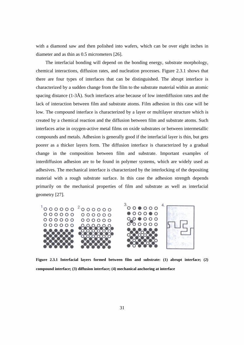
31
with a diamond saw and then polished into wafers, which can be over eight inches in
diameter and as thin as 0.5 micrometers [26].
The interfacial bonding will depend on the bonding energy, substrate morphology,
chemical interactions, diffusion rates, and nucleation processes. Figure 2.3.1 shows that
there are four types of interfaces that can be distinguished. The abrupt interface is
characterized by a sudden change from the film to the substrate material within an atomic
spacing distance (1-3Å). Such interfaces arise because of low interdiffusion rates and the
lack of interaction between film and substrate atoms. Film adhesion in this case will be
low. The compound interface is characterized by a layer or multilayer structure which is
created by a chemical reaction and the diffusion between film and substrate atoms. Such
interfaces arise in oxygen-active metal films on oxide substrates or between intermetallic
compounds and metals. Adhesion is generally good if the interfacial layer is thin, but gets
poorer as a thicker layers form. The diffusion interface is characterized by a gradual
change in the composition between film and substrate. Important examples of
interdiffusion adhesion are to be found in polymer systems, which are widely used as
adhesives. The mechanical interface is characterized by the interlocking of the depositing
material with a rough substrate surface. In this case the adhesion strength depends
primarily on the mechanical properties of film and substrate as well as interfacial
geometry [27].
Figure 2.3.1 Interfacial layers formed between film and substrate: (1) abrupt interface; (2)
compound interface; (3) diffusion interface; (4) mechanical anchoring at interface
32
2.3.1 DBC Cu-Alumina interface
The Direct Bonded Copper (DBC) process is a high temperature process. It is based
on the physical fact that oxygen reduces the melting point from 1083°C to 1065°C
(Eutectic melting temperature). A thin layer of eutectic melt forms by oxidizing copper
foils or injecting oxygen during the high temperature annealing process, which is
between 1065°C and 1080°C. The melt reacts with the alumina by forming a very thin
copper-alunimum-spinel layer. The formation of the bonding is shown in Fig. 2.3.2. It is
possible to do the copper-to-copper fusing in the same way. The copper-AlN DBC is
formed by transforming the ALN surface into a 1-2 µm alumina layer with high
temperature oxidation as shown in Fig. 2.3.3 [28].
Copper
Ceramic
Copper
Ceramic
O2CopperOxide
Copper
Ceramic
EutecticMelt
Heating
O2 Diffusionand
CoolingCopper
Ceramic
Copper
Copper
Copper
Copper
Copper
Copper
Copper
Copper
AlN
4 AlN + 6 O2 ≈1200°C
2 Al2O3 +2 N2
1 - 2 µm Al2O3
AlN
Al2O3 DCB Process
Oxidation
AlN
4 AlN + 6 O2 ≈1200°C
2 Al2O3 +2 N2
1 - 2 µm Al2O3
AlN
Al2O3 DCB Process
Oxidation
(a) (b)
Figure 2.3.2 DBC copper-ceramic bonding process (a) Alumina DBC; (b) AlN DBC process reaction
2.3.2 Inter-metallic interfaces
The metal depositions on silicon and on high dielectric constant ceramic tiles are
processed in a different way from DBC. In planar integration technology, the substrates
are pre-cleaned thoroughly. Then a thin layer of titanium is sputtered on the substrate.
Physical sputtering is a non-thermal vaporization process where surface atoms are
physically ejected from a solid surface by momentum transfer from an atomic-sized
energetic bombarding particle which is usually a gaseous ion accelerated from plasma
[29]. In the early years of semiconductor electronics, thin films of metals were typically
33
deposited by electro-beam (e-beam) or hot filament evaporation. However, in recent year
sputtering has begun to displace evaporation. There are a number of reasons why
Physical Vapor Deposition (PVD) has been so successful for microelectronics
applications. The sputtering can be used to deposit all of the conducting films currently
used in interconnecting metallization schemes, including low-melting-point metals such
as Al (Tmelt=660°C) and refractory metals such as Ti (Tmelt=1670°C). The PVD
deposition rate is also well matched to the needs of the pf wafer fabrication process. The
sputtered film attributes, such as purity and microstructure, surface roughness, and film
adhesion to oxides, have all proven acceptable for microelectronics applications. Because
sputtering is done from an extended area target and not from a point source as in
evaporation, shadowing is minimized and the resulting step coverage is generally good.
Since PVD utilizes nontoxic targets and low pressures of inert gas (1-10 mTorr of Ar), it
also meets the increasing needs of environmental concerns. PVD is also compatible with
the established trend toward automated single-wafer, vacuum-integrated processing [30].
As shown in Fig. 2.1.1, the inter-metallic interfaces in the integrated modules include
an Al-Ti interface and an Ti-Cu interface. Al, Ti, and Cu are all very popular metals used
in the IC industry. The advantages of Al in microelectronics are numerous [31]. The
room temperature electrical resistivity of pure Al (ρ=2.7 µΩ-cm), although not as low as
Cu, Ag and Au, is one of the lowest of all the metals. The DC magnetron sputter rate of
Al is high (>1µm/min). Although Al is highly reactive with SiO2 and reduces it to Si, the
reaction is self-limiting and stops when a sufficiently thick Al2O3 layer has been formed.
Al also has a relatively low melting point with high self-diffusion rates at moderate
process temperatures (400-550°C). This has allowed a variety of elevated-temperature
PVD processes such as the reflowed Al and the cold-hot Al, a two-step process (TSP), to
be used to improve the step coverage and filling of Al in high aspect ratio features. Al
films and Al alloy films with moderate weight percents of Cu can be readily patterned
into interconnecting lines using plasma-assisted, dry etching methods. Two major
concerns about PVD Al interconnecting lines are their relatively poor electromigration
(EM) resistance and the effects of stress that can result in the formation of voids within
the lines or the formation of protruding bumps on their surface (hillock formation).
Electromigration refers to the migration of matter due to momentum exchange between
34
the conduction electrons and Al atoms of the interconnecting line. Even though the total
current flow in a thin film interconnection is small, its microscopic cross-sectional area
leads to an enormous current density (106-7 A/cm2 for advanced devices), which can
lower device reliability and even result in catastrophic open-circuit line failure [32].
Copper is a promising candidate to replace Al in ULSI metallization for better
conductivity and reliability. Electroplating, in comparison with electroless plating, can
provide a higher deposition rate. Moreover, electroplating solutions for copper deposition
are more stable and easier to control [33]. Resistivity of electroplated Cu films was about
1.8-2µΩ.cm when the thickness of electroplated copper films exceeded 0.5 µm. Low
temperature annealing of electroplated Cu films resulted in further reduction in resistivity
[33].
However, Copper is considered to be a serious contamination in silicon wafer
processing. Copper exhibits deep level in the silicon band gap that acts as a
recombination center for carrier reducing drain current. Cu impurities in gate/tunnel
oxides compromise the dielectric integrity leading to leakage. A diffusion barrier is
usually used to prevent Cu diffusion into a silicon dioxide [34].
In the semiconductor industry, diffusion barrier layers are used in metallization
systems to prevent the diffusion and reaction of the deposited metallization material with
the silicon in subsequent high temperature processing. The titanium serves primarily as
an adhesion layer and diffusion barrier layer in the semiconductor industry. Ti has a
relatively high melting point. The refractory metals such as Ti and W do not react with Si
to form silicide until 600°C [35]. Ti is an oxygen active material. Ti layer will react with
oxide surfaces to achieve a good adhesion and contaminant-free surface.
Another reason to add a Ti layer is because direct contact of Cu and Al can form
Al2Cu precipitates, which can increase the corrosion of the metal after it has been
patterned by reactive ion etching [36]. A Ti layer can effectively prevent Cu diffusion
into adjacent materials during device processing and/or operation, especially in an
electrical field, which may lead to leakage currents, degraded performance, and device
failure [37].
Extensive research has been done to investigate the interface properties of these
metals in thin film areas. Since the sputter process used in our integration technology is

35
similar to that used in the thin film technology, and the thickness of sputtered Ti and Cu
films are of the typical thin film thicknesses, the thin film interface research
achievements are valuable for our study to understand the inter-metallic interface
properties. Research on Al-Ti interface shows that the sputtered Al and Ti interface
appears atomically abrupt. However, the inter-diffusion on an atomic scale cannot be
ruled out due to the heating of the substrate during processing. Annealing of the
multilayered structure at a temperature of 400°C (0.72 Tm of Al) leads to the disruption
of the layered structure by the inter-diffusion of Ti and Al, followed by a chemical
reaction. The chemical reaction results in precipitation of fine Al3Ti. Al3Ti is
thermodynamically the most stable Al-Ti inter-metallic compound. Al3Ti precipitates
appear evenly distributed in the annealed samples. With the progress of annealing, the
layered structure was completely replaced by an Al-Al3Ti dual phase microstructure with
AL3Ti dispersed evenly and mostly at the Al grain boundaries. With the increase in the
time of annealing, the size of Al grains and Al3Ti particles increased [38].
Copper suffers from some problems in its use as a multilevel interconnection. It has
a relatively poor adhesion to SiO2, and diffuses rather rapidly into Si. Both of these
effects can be controlled through the use of a properly selected diffusion barrier. Ti is an
excellent choice for this application. However, Ti and Cu will interact at temperatures
that are likely to be encountered during metallization anneals. The stresses generated by
these interactions may change due to the formation of new compounds. TiCu and TiCu3
are new compounds found in the Cu-Ti interface [39].
2.3.3 Surface roughness of different substrates
The detailed interfaces of integrated active modules and passive modules are listed in
Fig. 2.3.3 (a) and (b). The surface condition is also an important factor to affect the
adhesion of the metal deposition. The surface profiles of the Al2O3 ceramic substrate, the
high permittivity ceramic tile, the glass substrate after sand blasting, and the polymer
layer are all shown in Fig. 2.3.4. All the measurement lengths are 5mm.
36
Al Pad on Chip
Drain Contact(Solderable)
Si IGBT or MOSFET Chip
Sputtered TiSputtered CuPlated CuPolyimide
Interlayer
Ceramic
Passivation Eposxy
Al Pad on Chip
Drain Contact(Solderable)
Si IGBT or MOSFET Chip
Sputtered TiSputtered CuPlated CuPolyimide
Interlayer
Ceramic
Passivation Al Pad on Chip
Drain Contact(Solderable)
Si IGBT or MOSFET Chip
Sputtered TiSputtered CuPlated CuPolyimide
Interlayer
Ceramic
Passivation Eposxy
(a) Inter-metallic interfaces of Embedded Power modules
Sputtered copper (400-500nm)
Ceramic substrate (150-600µm)
Titanium (250nm)
Electroplated copper (100µm)
(b) Material layers in integrated passive modules
Figure 2.3.3 Cross-section view of metallized substrates. (a) Inter-metallic interfaces of Embedded
Power modules. (b) Material layers in Passive IPEMs.
-20000
-15000
-10000
-5000
0
5000
10000
15000
20000
25000Measurement Length 5mm
Surface waviness 2.7µm
Angstrom
(10-10 m)
-20000
-15000
-10000
-5000
0
5000
10000
15000
20000
25000Measurement Length 5mm
Surface waviness 2.7µm
Angstrom
(10-10 m)
-120000
-100000
-80000
-60000
-40000
-20000
0
20000
40000
60000
Measurement Length 5mm
Surface waviness 12 µm
Angstrom
(10-10 m)
-120000
-100000
-80000
-60000
-40000
-20000
0
20000
40000
60000
Measurement Length 5mm
Surface waviness 12 µm
Angstrom
(10-10 m)
(a) surface profile of Al2O3 (b) Surface profile of polymer
-150000
-100000
-50000
0
50000
100000
150000
200000
250000
300000
Measurement Length 5mm
Surface waviness 37µm
Angstrom
(10-10 m)
-150000
-100000
-50000
0
50000
100000
150000
200000
250000
300000
Measurement Length 5mm
Surface waviness 37µm
Angstrom
(10-10 m)
-400
-300
-200
-100
0
100
200
300
Measurement Length 5mm
Surface waviness 0.045µm
Angstrom
(10-10 m)
-400
-300
-200
-100
0
100
200
300
Measurement Length 5mm
Surface waviness 0.045µm
Angstrom
(10-10 m)
(c) surface profile of Y5V (d) surface profile of glass substrate
Figure 2.3.4 Surface profiles of different substrates. (a)Al2O3; (b) Polymer; (c)Y5V ceramics; (d)glass
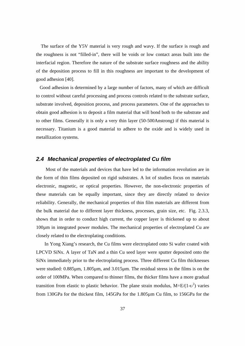
37
The surface of the Y5V material is very rough and wavy. If the surface is rough and
the roughness is not “filled-in”, there will be voids or low contact areas built into the
interfacial region. Therefore the nature of the substrate surface roughness and the ability
of the deposition process to fill in this roughness are important to the development of
good adhesion [40].
Good adhesion is determined by a large number of factors, many of which are difficult
to control without careful processing and process controls related to the substrate surface,
substrate involved, deposition process, and process parameters. One of the approaches to
obtain good adhesion is to deposit a film material that will bond both to the substrate and
to other films. Generally it is only a very thin layer (50-500Anstrong) if this material is
necessary. Titanium is a good material to adhere to the oxide and is widely used in
metallization systems.
2.4 Mechanical properties of electroplated Cu film
Most of the materials and devices that have led to the information revolution are in
the form of thin films deposited on rigid substrates. A lot of studies focus on materials
electronic, magnetic, or optical properties. However, the non-electronic properties of
these materials can be equally important, since they are directly related to device
reliability. Generally, the mechanical properties of thin film materials are different from
the bulk material due to different layer thickness, processes, grain size, etc. Fig. 2.3.3,
shows that in order to conduct high current, the copper layer is thickened up to about
100µm in integrated power modules. The mechanical properties of electroplated Cu are
closely related to the electroplating conditions.
In Yong Xiang’s research, the Cu films were electroplated onto Si wafer coated with
LPCVD SiNx. A layer of TaN and a thin Cu seed layer were sputter deposited onto the
SiNx immediately prior to the electroplating process. Three different Cu film thicknesses
were studied: 0.885µm, 1.805µm, and 3.015µm. The residual stress in the films is on the
order of 100MPa. When compared to thinner films, the thicker films have a more gradual
transition from elastic to plastic behavior. The plane strain modulus, M=E/(1-υ2) varies
from 130GPa for the thickest film, 145GPa for the 1.805µm Cu film, to 156GPa for the
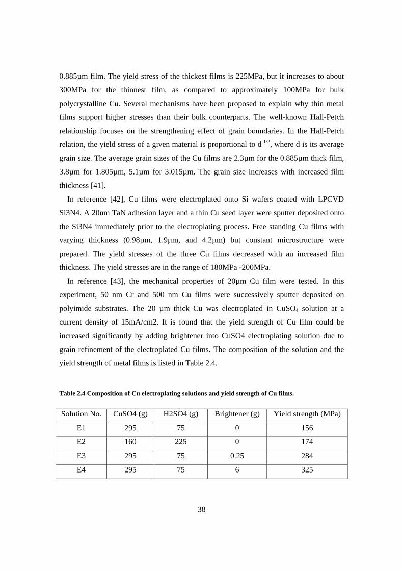
38
0.885µm film. The yield stress of the thickest films is 225MPa, but it increases to about
300MPa for the thinnest film, as compared to approximately 100MPa for bulk
polycrystalline Cu. Several mechanisms have been proposed to explain why thin metal
films support higher stresses than their bulk counterparts. The well-known Hall-Petch
relationship focuses on the strengthening effect of grain boundaries. In the Hall-Petch
relation, the yield stress of a given material is proportional to d-1/2, where d is its average
grain size. The average grain sizes of the Cu films are 2.3µm for the 0.885µm thick film,
3.8µm for 1.805µm, 5.1µm for 3.015µm. The grain size increases with increased film
thickness [41].
In reference [42], Cu films were electroplated onto Si wafers coated with LPCVD
Si3N4. A 20nm TaN adhesion layer and a thin Cu seed layer were sputter deposited onto
the Si3N4 immediately prior to the electroplating process. Free standing Cu films with
varying thickness (0.98µm, 1.9µm, and 4.2µm) but constant microstructure were
prepared. The yield stresses of the three Cu films decreased with an increased film
thickness. The yield stresses are in the range of 180MPa -200MPa.
In reference [43], the mechanical properties of 20µm Cu film were tested. In this
experiment, 50 nm Cr and 500 nm Cu films were successively sputter deposited on
polyimide substrates. The 20 µm thick Cu was electroplated in CuSO4 solution at a
current density of 15mA/cm2. It is found that the yield strength of Cu film could be
increased significantly by adding brightener into CuSO4 electroplating solution due to
grain refinement of the electroplated Cu films. The composition of the solution and the
yield strength of metal films is listed in Table 2.4.
Table 2.4 Composition of Cu electroplating solutions and yield strength of Cu films.
Solution No. CuSO4 (g) H2SO4 (g) Brightener (g) Yield strength (MPa)
E1 295 75 0 156
E2 160 225 0 174
E3 295 75 0.25 284
E4 295 75 6 325
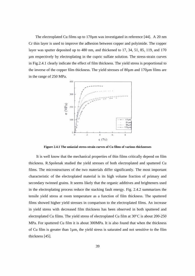
39
The electroplated Cu films up to 170µm was investigated in reference [44]. A 20 nm
Cr thin layer is used to improve the adhesion between copper and polyimide. The copper
layer was sputter deposited up to 480 nm, and thickened to 17, 34, 51, 85, 119, and 170
µm respectively by electroplating in the cupric sulfate solution. The stress-strain curves
in Fig.2.4.1 clearly indicate the effect of film thickness. The yield stress is proportional to
the inverse of the copper film thickness. The yield stresses of 80µm and 170µm films are
in the range of 250 MPa.
Figure 2.4.1 The uniaxial stress-strain curves of Cu films of various thicknesses
It is well know that the mechanical properties of thin films critically depend on film
thickness. R.Spolenak studied the yield stresses of both electroplated and sputtered Cu
films. The microstructures of the two materials differ significantly. The most important
characteristic of the electroplated material is its high volume fraction of primary and
secondary twinned grains. It seems likely that the organic additives and brighteners used
in the electroplating process reduce the stacking fault energy. Fig. 2.4.2 summarizes the
tensile yield stress at room temperature as a function of film thickness. The sputtered
films showed higher yield stresses in comparison to the electroplated films. An increase
in yield stress with decreased film thickness has been observed in both sputtered and
electroplated Cu films. The yield stress of electroplated Cu film at 30°C is about 200-250
MPa. For sputtered Cu film it is about 300MPa. It is also found that when the thickness
of Cu film is greater than 1µm, the yield stress is saturated and not sensitive to the film
thickness [45].
40
Figure 2.4.2 Tensile yield stress at 30°C as a function of film thickness for electroplated and
sputtered Cu
The previous results for electroplated Cu yield stress are summarized in Table 2.5.
All the research results agree that the yield stresses decrease with the increase in copper
film thickness. The yield stress is not sensitive to the film thickness once the film is
thicker than a few micrometers. Although the results varied due to different experimental
setup and test samples, the yield stress of electroplated copper film is in the range of
200MPa to 300MPa. Adding brightener will increase the yield stress dramatically (more
than 300MPa) due to the finer grain size. In our experiments, the brightener is added in
the Cu plating solution. The copper film is of up to 100µm thickness. The yield stress of
this copper film should be in the range of 250MPa ~350MPa. The value 300Mpa will be
chosen as the yield stress in Chapter 4 for FEA simulation.
Table 2.5 Research summary for electroplated copper film yield stress.
Reference Cu thickness Yield stress Description
[41] 3.015µm ~275 MPa TaN as barrier
[42] 4.2µm ~180MPa TaN as barrier
[43] 20µm 284/325MPa Brightener added 0.25g/6g
[44] 170µm ~250MPa 20nm Cr as barrier
[45] 1.7µm ~200-250MPa 50nm Ta as barrier
41
2.5 Effect of film intrinsic residual stress
Because many thin film processes are at elevated temperatures, it follows that very
large thermal stresses are induced in these materials during the manufacture process and
remain there during the subsequent use of the devices. There are additional stresses, so-
called “intrinsic stresses” being produced by non-equilibrium growth processes. These
non-equilibrium microstructures lead to additional stresses caused by the tendency of the
film to shrink or expand once it has been deposited onto its substrate. When film
thickness and substrate thickness are compatible, especially when the substrate is a brittle
material, the compressive stresses in the films can be so great that the corresponding
tensile stresses in the uppermost layer of the substrate can cause the fracture of the
substrate. The fracture, in turn, can cause electrical shorts to occur in the circuit if two
metallization layers are in contact. Or it might lead to some form of delayed failure of the
interconnecting metal. Such delayed failures might involve either corrosion of the
interconnecting metal or electro-migration. It is important to understand the mechanisms
of the residual stresses and the mechanical properties of the films so that the circuit
structures can be designed for mechanical reliability as well as for electronic device
performance [46].
The film under compression will expand if the substrate is thin, and the film will bow
the substrate so that the film is on the convex side. If the film has a tensile stress, the film
will contract, bowing the substrate so that the film is on the concave side. Tensile stress
will relieve itself by microcracking the film. Compressive stress will relieve itself by
bucking from contamination of the surface. If the adhesion between the film and the
substrate is high, the stress can cause a fracture in the film or substrate material rather
than at the interface. Compressive stress in a ductile material can relieve itself by
generating hillocks [47].
In power passive modules, delamination can cause a decrease in the effective
contact area to realize the capacitor. This may shift the resonant frequency of the LC
module, which may cause the failure of the electrical circuits operation. For the
embedded power modules, the delamination of the copper from silicon may cause them
to end up with an open circuit. It may also burn the other switching devices at the system
level. A compressive stress can result in film buckling and delamination, whereas an
42
excessive tensile stress may lead to film or substrate cracking. In integrated passive
modules, the sputtered metal particles on the cracking surface developed all the way
through the brittle ceramic substrates causing a short circuit between top and bottom
metallization. In integrated active modules, the silicon crack can disturb the functions of
the normal silicon devices.
In this chapter, manufacturing processes of planar integrated power electronics
modules are briefly introduced. One of the main features of IPEMs is that there are metal
depositions on top of brittle substrates. The interface conditions and mechanical
properties of electroplated copper are reviewed by literature research. The effect of
intrinsic residual stress is the starting point to investigate the stress effects on reliability
of the modules. In the next chapter, the background information about residual stress and
the experimental method to measure the residual stress induced during processes will be
covered.
43
Chapter 3: Intrinsic Residual Stress Residual stress plays a significant role in the reliability of thin micro-electro-
mechanical systems (MEMS) because the planar metallization structure is adopted in
high power, high current power application. The residual stress induced by the integrated
planar technology is worth investigating in order to understand the reliable operation of
integrated power modules. The basic investigation methodologies used in thin film
studies are still effective tools for our integrated power modules.
There are essentially two types of residual stresses. One type is strongly temperature
dependent. It is generated because of different thermal expansion coefficients of different
material layers. The second type of stress is intrinsic. It is process and film growth related,
and will generally be temperature independent. Factors responsible for this type of stress
include deposition conditions, the growth morphology, and the possible lattice mismatch
between layers. The residual stress investigated in this study is the second type: intrinsic
residual stress.
3.1 Introduction and Literature Review
Residual stress is a tension or compression stress that exists in a material without
application of an external load. Residual stresses arise in castings, welds, machined and
ground materials and heat treatment processes. Over the years many investigations have
been done to explain the causes of the intrinsic residual stress. Those mechanisms can be
divided into those that are operative within films (f) and those that are operative at the
film-substrate (f-s) level [48].
1. Differences in thermal expansion coefficients of film and substrate (f-s)
2. Incorporation of atoms, such as residual gases, or chemical reactions (f)
3. Lattice mismatch between films and substrates during epitaxial growth (f-s)
4. Variation of the interatomic spacing with crystal size (f)
5. Recrystallization processes (f)
6. Microscopic voids and special arrangements of dislocations (f, f-s)
7. Phase transformations (f,f-s)

44
As shown in Fig. 3.1.1, when the film initially shrinks relative to the substrate, the film is
under residual tensile stress. When the film expands relative to the substrate, there is
compressive stress on the film. These results are regardless of the specific mechanisms
that cause films to stretch or shrink relative to substrates. Sometimes the tensile stresses
are sufficiently large to cause a film fracture. Similarly, excessively high compressive
stresses can cause film wrinkling and local loss of adhesion to the substrate. Usually the
residual stresses are undesirable, but there are cases where the compressive stress is
introduced to counteract the harmful tensile stresses for brittle materials [49].
Figure 3.1.1 residual tensile and compressive stress in the film
Experimental techniques for measuring stress in thin films on substrate can be
classified into two large categories: (a) lattice strain based methods, including X-ray and
neutron diffraction, and (b) physical surface curvature-based methods. X-ray diffraction-
based methods have usually been limited to crystalline thin films because they rely on the
measurement for the variation of lattice spacing. On the other hand, the techniques based
on curvature measurement can readily apply to both crystalline and non-crystalline thin
films [50]. The curvature and layer removal techniques are often used for measuring the
presence of residual stress in simple test piece geometries. The methods are generally
quick and require only simple calculations to relate the curvature to the residual stresses.
When layers are removed from one side of a flat plate containing residual stresses, the
stresses become unbalanced and the plate bends. The curvature depends on the original
stress distribution present in the layer that has been removed and on the elastic properties
of the remainder of the plate. By carrying out a series of curvature measurements after
45
successive layer removals the distribution of stress in the original plate can then be
deduced.
The curvature of the specimen can be measured using a variety of methods including
optical microscopy, laser scanning, strain gauges, or profilometry, depending on the
resolution and range of the measuring instrument. Measurements are usually made on
narrow strips to avoid multi-axial curvature and mechanical instability. The method uses
the basic principles by measuring changes in curvature to calculate residual stress. The
simplified glass-copper structure is used to study the intrinsic residual stress induced
during the process.
3.2 Measurement of Intrinsic Residual Stress in Glass-metal
Structure
Experimentally measuring the residual stress is very challenging work in
complicated structures. In our experiments, a glass metal structure is used as the
experiment sample. The identical copper deposition processes used in integrated
technology is also used to develop the test samples. The sample curvatures are measured
by the DEKTAK surface profile measuring system. The residual stresses are calculated
using the Stoney equation. The details are presented in the follow chapters.
3.2.1 Sample preparation
The test samples for intrinsic residual stress measurement used glass as the substrate
instead of the ceramic because the ceramic surface is too rough for the DEKTAK surface
profile measuring system. The glass used is laboratory equipment from Corning Lab &
Equipment Company. Because of the glass manufacturing process, some glass samples
are not flat enough for our measurement purpose. Some samples have a big original
bending, which is comparable to the bending that occurs after electroplating. So one of
the two purposes for selecting samples is to select those which have the smallest original
bending. The other purpose is to choose the samples that have the smallest surface
waviness. Surface waviness is defined as the distance between the highest point and the
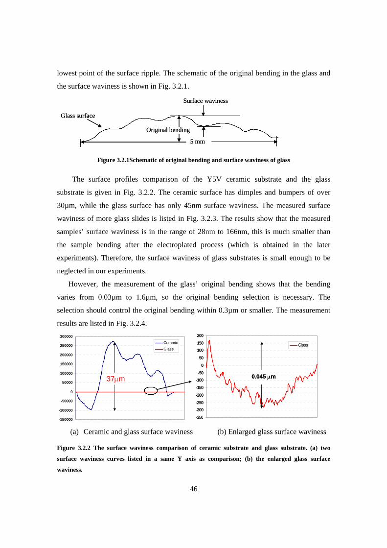
46
lowest point of the surface ripple. The schematic of the original bending in the glass and
the surface waviness is shown in Fig. 3.2.1.
Glass surface
Surface waviness
5 mm
Original bending
Glass surface
Surface waviness
5 mm
Original bending
Figure 3.2.1Schematic of original bending and surface waviness of glass
The surface profiles comparison of the Y5V ceramic substrate and the glass
substrate is given in Fig. 3.2.2. The ceramic surface has dimples and bumpers of over
30µm, while the glass surface has only 45nm surface waviness. The measured surface
waviness of more glass slides is listed in Fig. 3.2.3. The results show that the measured
samples’ surface waviness is in the range of 28nm to 166nm, this is much smaller than
the sample bending after the electroplated process (which is obtained in the later
experiments). Therefore, the surface waviness of glass substrates is small enough to be
neglected in our experiments.
However, the measurement of the glass’ original bending shows that the bending
varies from 0.03µm to 1.6µm, so the original bending selection is necessary. The
selection should control the original bending within 0.3µm or smaller. The measurement
results are listed in Fig. 3.2.4.
-150000
-100000
-50000
0
50000
100000
150000
200000
250000
300000CeramicGlass
-350-300-250-200-150-100-50
050
100150200
Glass
0.045 µm0.045 µm37µm
(a) Ceramic and glass surface waviness (b) Enlarged glass surface waviness
Figure 3.2.2 The surface waviness comparison of ceramic substrate and glass substrate. (a) two
surface waviness curves listed in a same Y axis as comparison; (b) the enlarged glass surface
waviness.
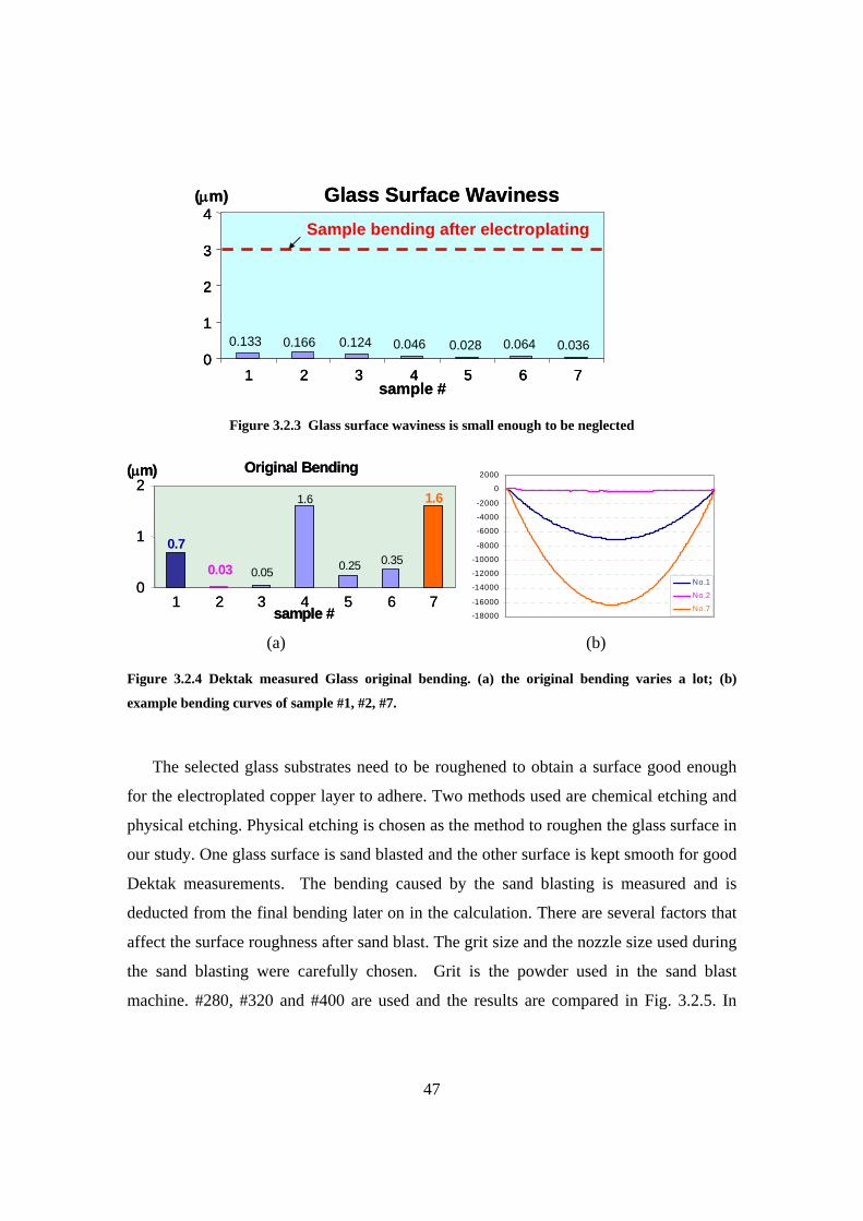
47
0.133 0.124 0.046 0.028 0.064 0.0360.1660
1
2
3
4
1 2 3 4 5 6 7
Glass Surface Waviness
sample #
(µm)
0.133 0.124 0.046 0.028 0.064 0.0360.1660
1
2
3
4
1 2 3 4 5 6 7
0.133 0.124 0.046 0.028 0.064 0.0360.1660
1
2
3
4
1 2 3 4 5 6 7
Glass Surface Waviness
sample #
(µm)
Sample bending after electroplating
Figure 3.2.3 Glass surface waviness is small enough to be neglected
Original Bending
0.7
0.03 0.05
1.6
0.25 0.35
1.6
0
1
2
sample #
(µm)
1 2 3 4 5 6 7
Original Bending
0.7
0.03 0.05
1.6
0.25 0.35
1.6
0
1
2
sample #
(µm)
1 2 3 4 5 6 7 -18000
-16000
-14000
-12000
-10000
-8000
-6000
-4000
-2000
0
2000
No.1
No.2
No.7
(a) (b)
Figure 3.2.4 Dektak measured Glass original bending. (a) the original bending varies a lot; (b)
example bending curves of sample #1, #2, #7.
The selected glass substrates need to be roughened to obtain a surface good enough
for the electroplated copper layer to adhere. Two methods used are chemical etching and
physical etching. Physical etching is chosen as the method to roughen the glass surface in
our study. One glass surface is sand blasted and the other surface is kept smooth for good
Dektak measurements. The bending caused by the sand blasting is measured and is
deducted from the final bending later on in the calculation. There are several factors that
affect the surface roughness after sand blast. The grit size and the nozzle size used during
the sand blasting were carefully chosen. Grit is the powder used in the sand blast
machine. #280, #320 and #400 are used and the results are compared in Fig. 3.2.5. In
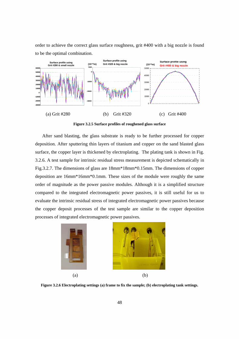
48
order to achieve the correct glass surface roughness, grit #400 with a big nozzle is found
to be the optimal combination.
Surface profile using Grit #280 & small nozzle
-30000
-20000
-10000
0
10000
20000
30000
40000
50000
60000
-30000
-20000
-10000
0
10000
20000
30000
40000
50000
60000
(10-10m)Surface profile using Grit #320 & big nozzle
-30000
-20000
-10000
0
5000
-30000
-20000
-10000
0
5000
0
10000
20000
30000
40000
50000
Surface profile usingGrit #400 & big nozzle(10-10m)
(a) Grit #280 (b) Grit #320 (c) Grit #400
Figure 3.2.5 Surface profiles of roughened glass surface
After sand blasting, the glass substrate is ready to be further processed for copper
deposition. After sputtering thin layers of titanium and copper on the sand blasted glass
surface, the copper layer is thickened by electroplating. The plating tank is shown in Fig.
3.2.6. A test sample for intrinsic residual stress measurement is depicted schematically in
Fig.3.2.7. The dimensions of glass are 18mm*18mm*0.15mm. The dimensions of copper
deposition are 16mm*16mm*0.1mm. These sizes of the module were roughly the same
order of magnitude as the power passive modules. Although it is a simplified structure
compared to the integrated electromagnetic power passives, it is still useful for us to
evaluate the intrinsic residual stress of integrated electromagnetic power passives because
the copper deposit processes of the test sample are similar to the copper deposition
processes of integrated electromagnetic power passives.
(a) (b)
Figure 3.2.6 Electroplating settings (a) frame to fix the sample; (b) electroplating tank settings.
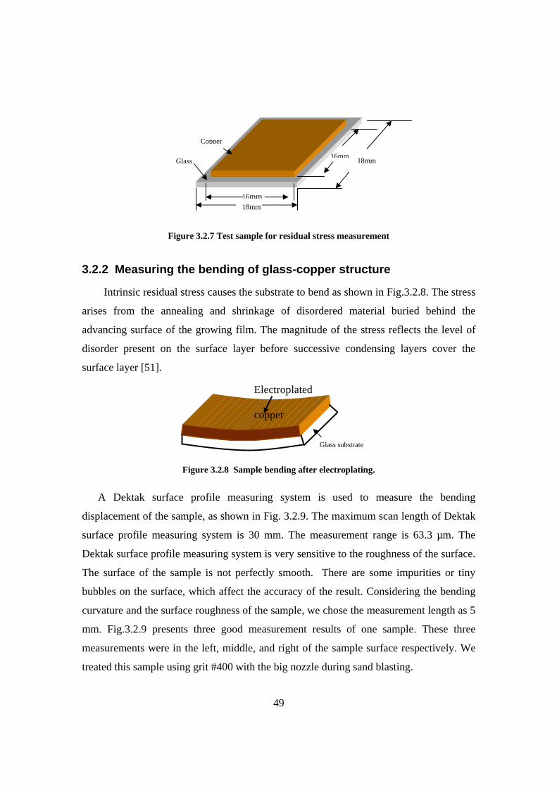
49
Figure 3.2.7 Test sample for residual stress measurement
3.2.2 Measuring the bending of glass-copper structure
Intrinsic residual stress causes the substrate to bend as shown in Fig.3.2.8. The stress
arises from the annealing and shrinkage of disordered material buried behind the
advancing surface of the growing film. The magnitude of the stress reflects the level of
disorder present on the surface layer before successive condensing layers cover the
surface layer [51].
Figure 3.2.8 Sample bending after electroplating.
A Dektak surface profile measuring system is used to measure the bending
displacement of the sample, as shown in Fig. 3.2.9. The maximum scan length of Dektak
surface profile measuring system is 30 mm. The measurement range is 63.3 µm. The
Dektak surface profile measuring system is very sensitive to the roughness of the surface.
The surface of the sample is not perfectly smooth. There are some impurities or tiny
bubbles on the surface, which affect the accuracy of the result. Considering the bending
curvature and the surface roughness of the sample, we chose the measurement length as 5
mm. Fig.3.2.9 presents three good measurement results of one sample. These three
measurements were in the left, middle, and right of the sample surface respectively. We
treated this sample using grit #400 with the big nozzle during sand blasting.
Glass
16mm18mm
16mm 18mm
Copper
Electroplated
copper
Glass substrate
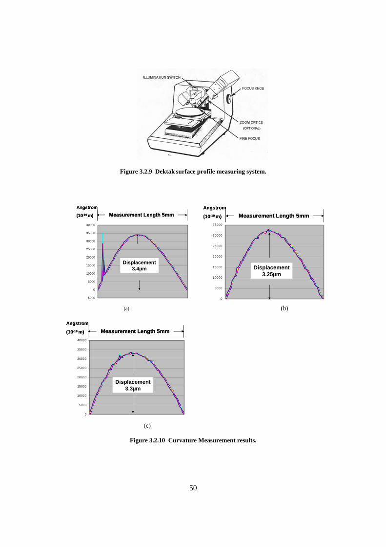
50
Figure 3.2.9 Dektak surface profile measuring system.
-5000
0
5000
10000
15000
20000
25000
30000
35000
40000
Measurement Length 5mm
Displacement 3.4µm
Angstrom
(10-10 m)
-5000
0
5000
10000
15000
20000
25000
30000
35000
40000
Measurement Length 5mm
Displacement 3.4µm
Angstrom
(10-10 m)
0
5000
10000
15000
20000
25000
30000
35000
Measurement Length 5mm
Displacement 3.25µm
Angstrom
(10-10 m)
0
5000
10000
15000
20000
25000
30000
35000
Measurement Length 5mm
Displacement 3.25µm
Angstrom
(10-10 m)
(a) (b)
0
5000
10000
15000
20000
25000
30000
35000
40000
Measurement Length 5mm
Displacement 3.3µm
Angstrom
(10-10 m)
0
5000
10000
15000
20000
25000
30000
35000
40000
Measurement Length 5mm
Displacement 3.3µm
Angstrom
(10-10 m)
(c)
Figure 3.2.10 Curvature Measurement results.
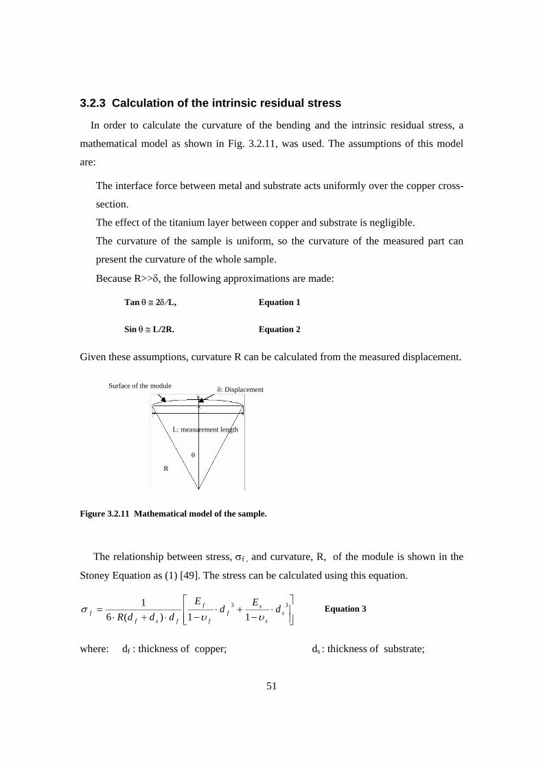
51
3.2.3 Calculation of the intrinsic residual stress
In order to calculate the curvature of the bending and the intrinsic residual stress, a
mathematical model as shown in Fig. 3.2.11, was used. The assumptions of this model
are:
The interface force between metal and substrate acts uniformly over the copper cross-
section.
The effect of the titanium layer between copper and substrate is negligible.
The curvature of the sample is uniform, so the curvature of the measured part can
present the curvature of the whole sample.
Because R>>δ, the following approximations are made:
Tan θ ≅ 2δ⁄ L, Equation 1
Sin θ ≅ L/2R. Equation 2
Given these assumptions, curvature R can be calculated from the measured displacement.
Figure 3.2.11 Mathematical model of the sample.
The relationship between stress, σf , and curvature, R, of the module is shown in the
Stoney Equation as (1) [49]. The stress can be calculated using this equation.
⎥⎥⎦
⎤
⎢⎢⎣
⎡⋅
−+⋅
−⋅+⋅= 33
11)(61
ss
sf
f
f
fsff d
Ed
EdddR υυ
σ Equation 3
where: df : thickness of copper; ds : thickness of substrate;
R
θ
L: measurement length
δ: Displacement Surface of the module
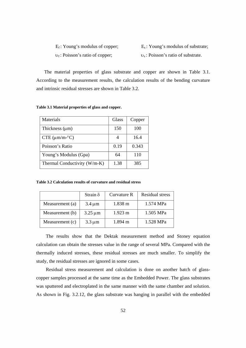
52
Ef : Young’s modulus of copper; Es : Young’s modulus of substrate;
υf : Poisson’s ratio of copper; υs : Poisson’s ratio of substrate.
The material properties of glass substrate and copper are shown in Table 3.1.
According to the measurement results, the calculation results of the bending curvature
and intrinsic residual stresses are shown in Table 3.2.
Table 3.1 Material properties of glass and copper.
Materials Glass Copper
Thickness (µm) 150 100
CTE (µm/m-°C) 4 16.4
Poisson’s Ratio 0.19 0.343
Young’s Modulus (Gpa) 64 110
Thermal Conductivity (W/m-K) 1.38 385
Table 3.2 Calculation results of curvature and residual stress
Strain δ Curvature R Residual stress
Measurement (a) 3.4 µm 1.838 m 1.574 MPa
Measurement (b) 3.25 µm 1.923 m 1.505 MPa
Measurement (c) 3.3 µm 1.894 m 1.528 MPa
The results show that the Dektak measurement method and Stoney equation
calculation can obtain the stresses value in the range of several MPa. Compared with the
thermally induced stresses, these residual stresses are much smaller. To simplify the
study, the residual stresses are ignored in some cases.
Residual stress measurement and calculation is done on another batch of glass-
copper samples processed at the same time as the Embedded Power. The glass substrates
was sputtered and electroplated in the same manner with the same chamber and solution.
As shown in Fig. 3.2.12, the glass substrate was hanging in parallel with the embedded
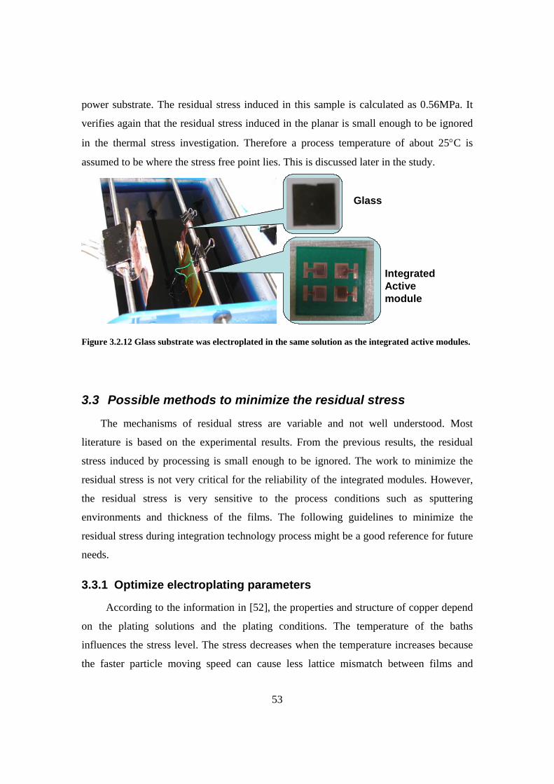
53
power substrate. The residual stress induced in this sample is calculated as 0.56MPa. It
verifies again that the residual stress induced in the planar is small enough to be ignored
in the thermal stress investigation. Therefore a process temperature of about 25°C is
assumed to be where the stress free point lies. This is discussed later in the study.
Glass
Integrated Active module
Figure 3.2.12 Glass substrate was electroplated in the same solution as the integrated active modules.
3.3 Possible methods to minimize the residual stress
The mechanisms of residual stress are variable and not well understood. Most
literature is based on the experimental results. From the previous results, the residual
stress induced by processing is small enough to be ignored. The work to minimize the
residual stress is not very critical for the reliability of the integrated modules. However,
the residual stress is very sensitive to the process conditions such as sputtering
environments and thickness of the films. The following guidelines to minimize the
residual stress during integration technology process might be a good reference for future
needs.
3.3.1 Optimize electroplating parameters
According to the information in [52], the properties and structure of copper depend
on the plating solutions and the plating conditions. The temperature of the baths
influences the stress level. The stress decreases when the temperature increases because
the faster particle moving speed can cause less lattice mismatch between films and
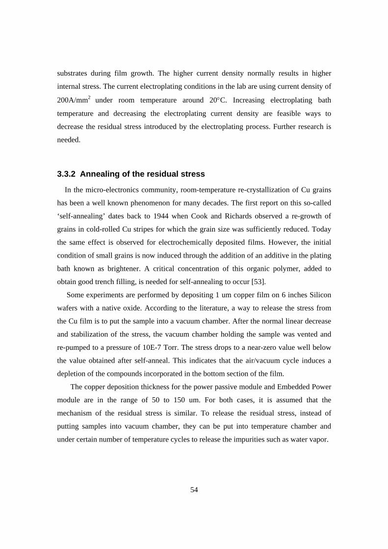
54
substrates during film growth. The higher current density normally results in higher
internal stress. The current electroplating conditions in the lab are using current density of
200A/mm2 under room temperature around 20°C. Increasing electroplating bath
temperature and decreasing the electroplating current density are feasible ways to
decrease the residual stress introduced by the electroplating process. Further research is
needed.
3.3.2 Annealing of the residual stress
In the micro-electronics community, room-temperature re-crystallization of Cu grains
has been a well known phenomenon for many decades. The first report on this so-called
‘self-annealing’ dates back to 1944 when Cook and Richards observed a re-growth of
grains in cold-rolled Cu stripes for which the grain size was sufficiently reduced. Today
the same effect is observed for electrochemically deposited films. However, the initial
condition of small grains is now induced through the addition of an additive in the plating
bath known as brightener. A critical concentration of this organic polymer, added to
obtain good trench filling, is needed for self-annealing to occur [53].
Some experiments are performed by depositing 1 um copper film on 6 inches Silicon
wafers with a native oxide. According to the literature, a way to release the stress from
the Cu film is to put the sample into a vacuum chamber. After the normal linear decrease
and stabilization of the stress, the vacuum chamber holding the sample was vented and
re-pumped to a pressure of 10E-7 Torr. The stress drops to a near-zero value well below
the value obtained after self-anneal. This indicates that the air/vacuum cycle induces a
depletion of the compounds incorporated in the bottom section of the film.
The copper deposition thickness for the power passive module and Embedded Power
module are in the range of 50 to 150 um. For both cases, it is assumed that the
mechanism of the residual stress is similar. To release the residual stress, instead of
putting samples into vacuum chamber, they can be put into temperature chamber and
under certain number of temperature cycles to release the impurities such as water vapor.
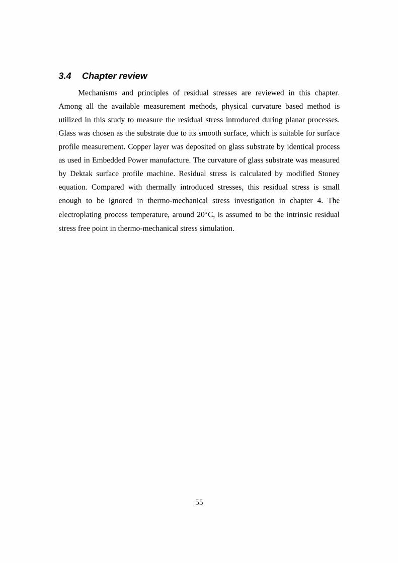
55
3.4 Chapter review
Mechanisms and principles of residual stresses are reviewed in this chapter.
Among all the available measurement methods, physical curvature based method is
utilized in this study to measure the residual stress introduced during planar processes.
Glass was chosen as the substrate due to its smooth surface, which is suitable for surface
profile measurement. Copper layer was deposited on glass substrate by identical process
as used in Embedded Power manufacture. The curvature of glass substrate was measured
by Dektak surface profile machine. Residual stress is calculated by modified Stoney
equation. Compared with thermally introduced stresses, this residual stress is small
enough to be ignored in thermo-mechanical stress investigation in chapter 4. The
electroplating process temperature, around 20°C, is assumed to be the intrinsic residual
stress free point in thermo-mechanical stress simulation.

56
Chapter 4: Thermo-mechanical Stresses in IPEMs Compared with residual stresses induced during manufacturing, the thermo-
mechanical stresses have more significant effects on the reliability and lifetimes of the
integrated modules. The temperature distributions in an Embedded Power module were
covered first. Due to the small gap between the temperatures of silicon devices and
deposited copper during the operation, the modules are assumed to be under same
temperature load during the stress modeling. A simplified bi-layer structure is used for
the stress modeling and simulation. Von Mises stress, shear stress, in-plane stress and
peel stress are modeled separated as the indicators of related failures. The modeling
results and simulation results are compared. The good agreement between the results
shows that the Finite Element Modeling software is an effective tool to study the
complicated structure. The complicated structures of the Embedded Power modules and
integrated passive modules are simulated to show the stress distribution.
4.1 Temperature Distribution in Embedded Power Module
The temperature distribution in an Embedded Power module is measured
experimentally and simulated in IDEAS software. The silicon devices are the hot spots
during operation. The time constant of the copper-silicon structure is verified to be small.
Therefore the temperatures of copper and silicon can be assumed to be the same in the
later study.
4.1.1 Simulation and experimental results
To understand the thermal behavior of the Embedded Power modules, a power
factor correction (PFC) IPEM was studied as a typical example in this part, as shown in
Fig. 4.1.1. The footprint of the PFC module is 34.2mm*29.7mm. Two CoolMOS chips
and two silicon carbide diodes are embedded into the module as the switching devices. A
commercial gate driver is attached in the module. The top surface of the module is
encapsulated with silicon gel for electrical isolation. The test module is attached to a
copper heat spreader and to an aluminum heat sink during the test. The module is placed
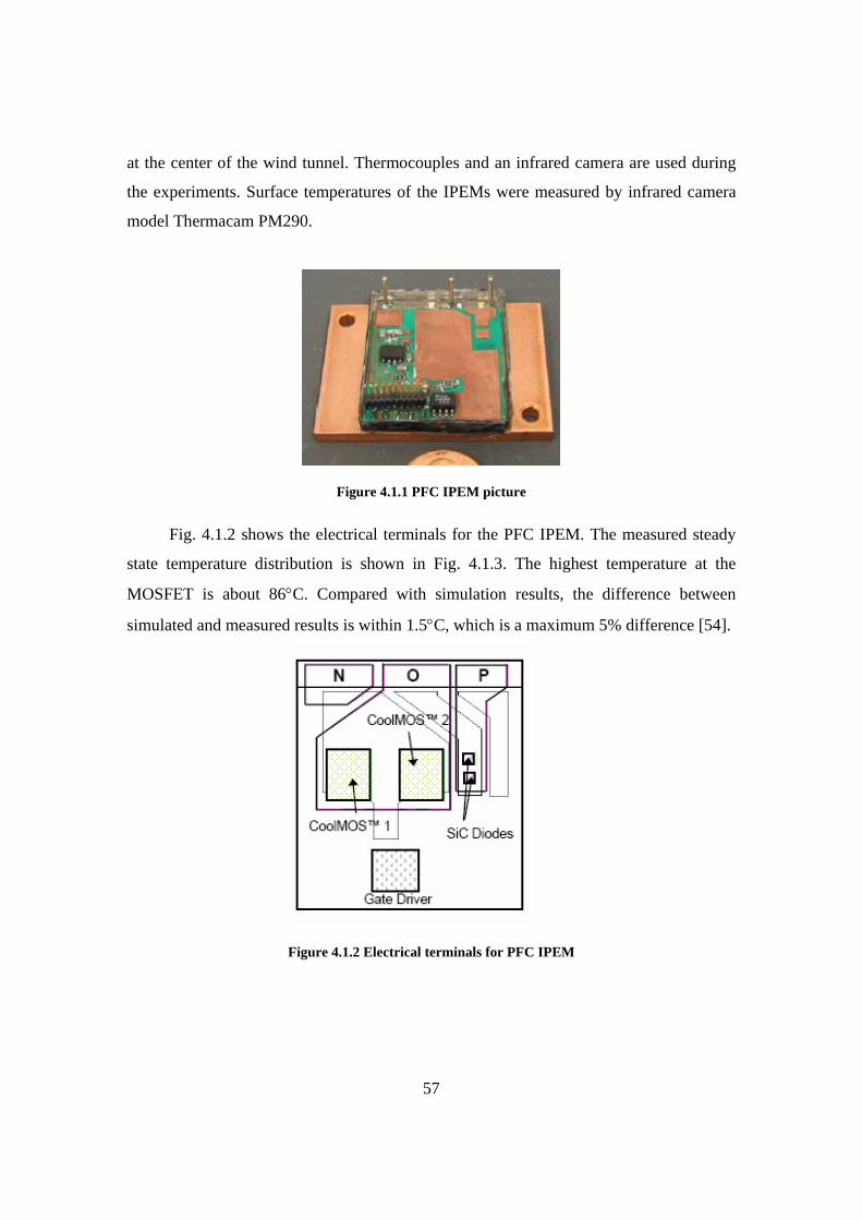
57
at the center of the wind tunnel. Thermocouples and an infrared camera are used during
the experiments. Surface temperatures of the IPEMs were measured by infrared camera
model Thermacam PM290.
Figure 4.1.1 PFC IPEM picture
Fig. 4.1.2 shows the electrical terminals for the PFC IPEM. The measured steady
state temperature distribution is shown in Fig. 4.1.3. The highest temperature at the
MOSFET is about 86°C. Compared with simulation results, the difference between
simulated and measured results is within 1.5°C, which is a maximum 5% difference [54].
Figure 4.1.2 Electrical terminals for PFC IPEM
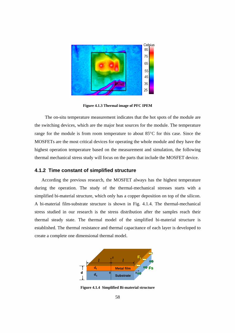
58
Figure 4.1.3 Thermal image of PFC IPEM
The on-situ temperature measurement indicates that the hot spots of the module are
the switching devices, which are the major heat sources for the module. The temperature
range for the module is from room temperature to about 85°C for this case. Since the
MOSFETs are the most critical devices for operating the whole module and they have the
highest operation temperature based on the measurement and simulation, the following
thermal mechanical stress study will focus on the parts that include the MOSFET device.
4.1.2 Time constant of simplified structure
According the previous research, the MOSFET always has the highest temperature
during the operation. The study of the thermal-mechanical stresses starts with a
simplified bi-material structure, which only has a copper deposition on top of the silicon.
A bi-material film-substrate structure is shown in Fig. 4.1.4. The thermal-mechanical
stress studied in our research is the stress distribution after the samples reach their
thermal steady state. The thermal model of the simplified bi-material structure is
established. The thermal resistance and thermal capacitance of each layer is developed to
create a complete one dimensional thermal model.
xdf
ds
Metal film
Substrated
l l
0
z Ff
Fsx
df
ds
Metal film
Substrated
l ll l
0
z Ff
Fs
Figure 4.1.4 Simplified Bi-material structure
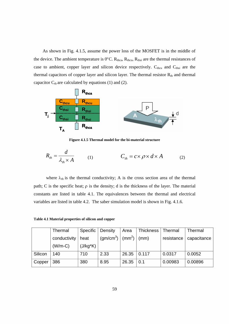
59
As shown in Fig. 4.1.5, assume the power loss of the MOSFET is in the middle of
the device. The ambient temperature is 0°C. Rthca, Rthcu, Rthsi are the thermal resistances of
case to ambient, copper layer and silicon device respectively. Cthcu and Cthsi are the
thermal capacitors of copper layer and silicon layer. The thermal resistor Rth and thermal
capacitor Cth are calculated by equations (1) and (2).
Rthca
Rthcu
Rthsi
Rthsi
Rthca
CthcuCthsi
Cthsi
TA
Tj
Rthca
Rthcu
Rthsi
Rthsi
Rthca
CthcuCthsi
Cthsi
Rthca
Rthcu
Rthsi
Rthsi
Rthca
CthcuCthsi
Cthsi
TA
Tj
Figure 4.1.5 Thermal model for the bi-material structure
AdR
thth ×=λ (1) AdcCth ×××= ρ (2)
where λth is the thermal conductivity; A is the cross section area of the thermal
path; C is the specific heat; ρ is the density; d is the thickness of the layer. The material
constants are listed in table 4.1. The equivalences between the thermal and electrical
variables are listed in table 4.2. The saber simulation model is shown in Fig. 4.1.6.
Table 4.1 Material properties of silicon and copper
Thermal
conductivity
(W/m-C)
Specific
heat
(J/kg*K)
Density
(gm/cm3)
Area
(mm2)
Thickness
(mm)
Thermal
resistance
Thermal
capacitance
Silicon 140 710 2.33 26.35 0.117 0.0317 0.0052
Copper 386 380 8.95 26.35 0.1 0.00983 0.00896
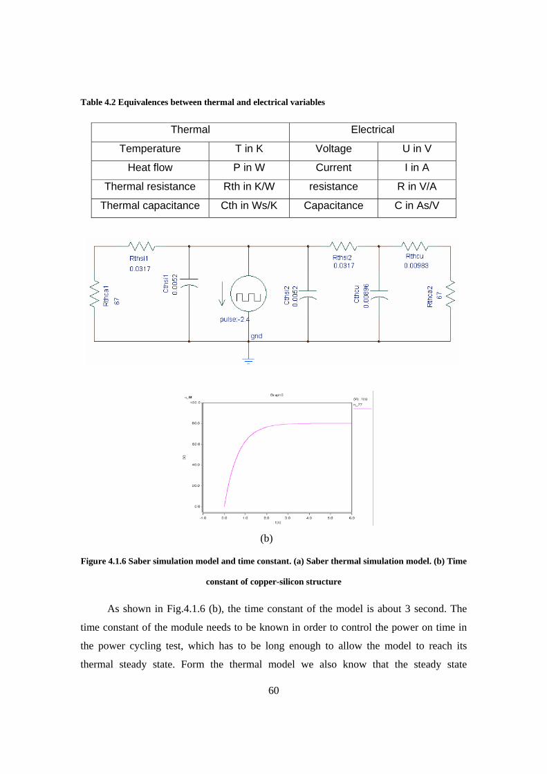
60
Table 4.2 Equivalences between thermal and electrical variables
Thermal Electrical
Temperature T in K Voltage U in V
Heat flow P in W Current I in A
Thermal resistance Rth in K/W resistance R in V/A
Thermal capacitance Cth in Ws/K Capacitance C in As/V
(b)
Figure 4.1.6 Saber simulation model and time constant. (a) Saber thermal simulation model. (b) Time
constant of copper-silicon structure
As shown in Fig.4.1.6 (b), the time constant of the model is about 3 second. The
time constant of the module needs to be known in order to control the power on time in
the power cycling test, which has to be long enough to allow the model to reach its
thermal steady state. Form the thermal model we also know that the steady state
61
temperature differences between silicon and copper is very small(less than 0.1°C). In
thermal mechanical stress model, it is assumed that the whole model has the same steady
state temperature.
4.2 Thermo-mechanical Stress in Simplified Structure
Thermal stresses in layered electronic assemblies result from the thermal and stiffness
mismatch of bonded materials. The bonding interfaces in such structures suffer high
stress concentrations, which eventually lead to the cracking of thin-layered structures or
interfacial delamination. The effect and reasonably accurate estimate of the stress level in
these structures is important to the design of the layered electronic assemblies [55].
Mechanical failure of an electrical device can be the result of one or any combination
of responses of the device to loads and environment. According to the features of the
materials used in integrated power electronics modules, Von Mises stress, peel stress,
shear stress and in-plane stress are investigated separately as the indicators of different
failure modes. Theoretical model and finite element analysis are the two methods used in
this chapter.
4.2.1 Von Mises stress
The major static failure modes of interest in the design of microelectronic
components are ductile rupture and brittle rupture. Ductile rupture occurs when the
plastic deformation in a material results in a progressive local reduction in cross-sectional
area. Von Mises theory states that a given material failure by yielding will occur at a
critical level of distortional energy. The criterion for no failure can be written as [56]
( ) ( ) ( )[ ] yps σσσσσσσ <−+−+−×= 212
132
322
2122
Equation 4
where S is Von Mises stress; σyp is the material yield stress.
BA −= )3
cos(1θσ Equation 5
62
BA −+= )3
23
cos(2πθσ Equation 6
BA −+= )3
43
cos(3πθσ Equation 7
with
QA −= 2 Equation 8
( ) 9/3 212 SSQ −= Equation 9
3/1SB = Equation 10
)(cos 31 QR −= −θ Equation 11
( ) 54/279 21321 SSSSR −−= Equation 12
( )zyxS σσσ ++−=1 Equation 13
2222 yzxzxyzyzxyxS τττσσσσσσ −−−++= Equation 14
( )2223 2 xyzxzyyzxxzyzxyzyxS τστστστττσσσ −−−+−= Equation 15
Checking the design by Von Mises theory is to compute the stresses in the assembly
and determine the locations where failure may be expected. If the value of S is less than
σyp, then there is no yielding and the design can be considered adequate; otherwise, the
design must be modified.
In the design of IPEMs, the copper or other metal deposition is the ductile material
suitable for the Von Mises theory. The yield stress of electroplated Cu is expected above
300MPa as discussed in Chapter2. The Von Mises stresses on the copper layer can be
found by finite element analysis simulation. A Cu-Si bi-layer structure under uniform
thermal load was simulated as an example. The silicon substrate has the dimensions of
18mm*18mm*0.15mm. The copper layers are rectangular shapes in the center of the
substrates. In Embedded Power modules, different shapes and widths of copper traces
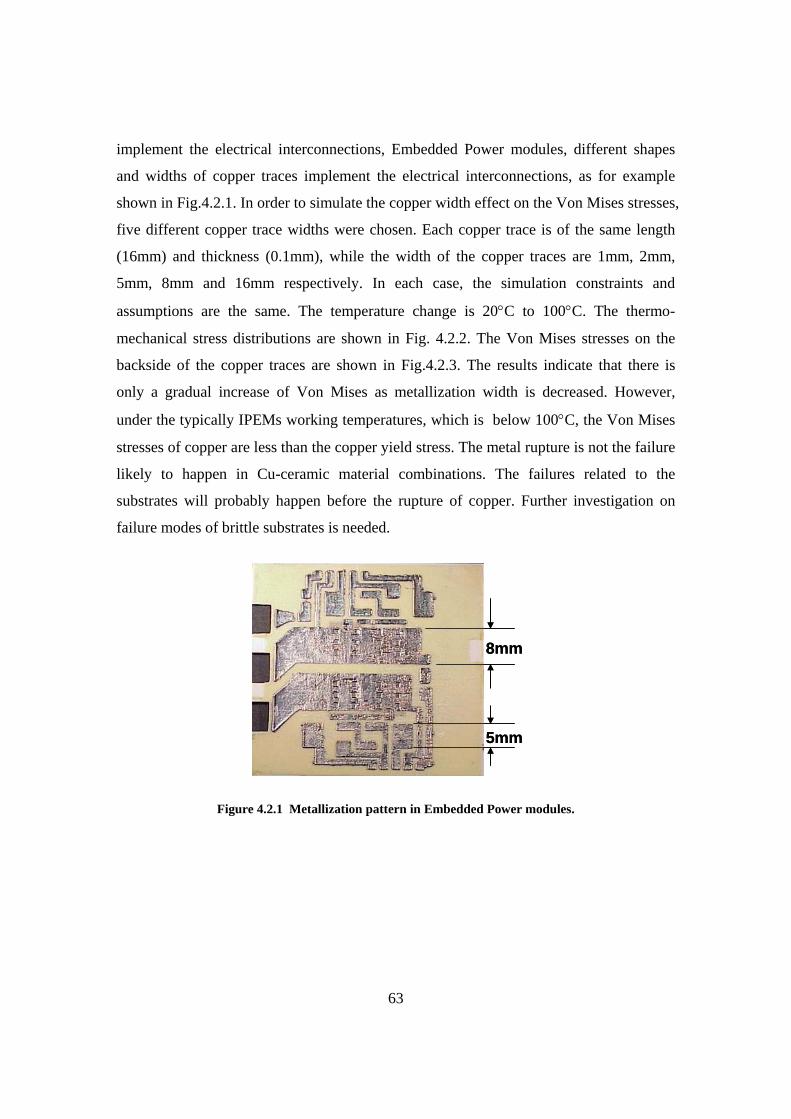
63
implement the electrical interconnections, Embedded Power modules, different shapes
and widths of copper traces implement the electrical interconnections, as for example
shown in Fig.4.2.1. In order to simulate the copper width effect on the Von Mises stresses,
five different copper trace widths were chosen. Each copper trace is of the same length
(16mm) and thickness (0.1mm), while the width of the copper traces are 1mm, 2mm,
5mm, 8mm and 16mm respectively. In each case, the simulation constraints and
assumptions are the same. The temperature change is 20°C to 100°C. The thermo-
mechanical stress distributions are shown in Fig. 4.2.2. The Von Mises stresses on the
backside of the copper traces are shown in Fig.4.2.3. The results indicate that there is
only a gradual increase of Von Mises as metallization width is decreased. However,
under the typically IPEMs working temperatures, which is below 100°C, the Von Mises
stresses of copper are less than the copper yield stress. The metal rupture is not the failure
likely to happen in Cu-ceramic material combinations. The failures related to the
substrates will probably happen before the rupture of copper. Further investigation on
failure modes of brittle substrates is needed.
8mm
5mm
8mm
5mm
Figure 4.2.1 Metallization pattern in Embedded Power modules.
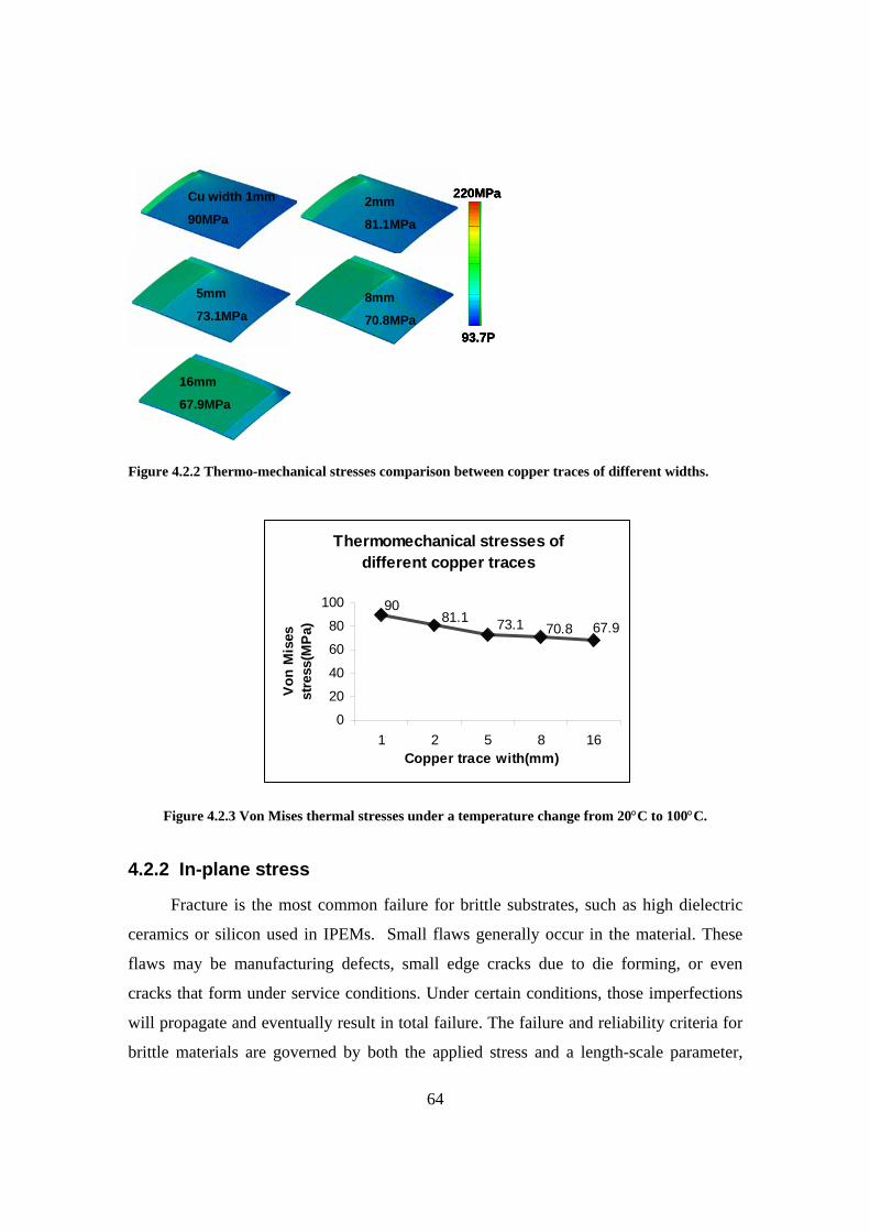
64
Figure 4.2.2 Thermo-mechanical stresses comparison between copper traces of different widths.
Thermomechanical stresses of different copper traces
67.970.8
9081.1 73.1
0
20
40
60
80
100
1 2 5 8 16Copper trace with(mm)
Von
Mis
es
stre
ss(M
Pa)
Figure 4.2.3 Von Mises thermal stresses under a temperature change from 20°C to 100°C.
4.2.2 In-plane stress
Fracture is the most common failure for brittle substrates, such as high dielectric
ceramics or silicon used in IPEMs. Small flaws generally occur in the material. These
flaws may be manufacturing defects, small edge cracks due to die forming, or even
cracks that form under service conditions. Under certain conditions, those imperfections
will propagate and eventually result in total failure. The failure and reliability criteria for
brittle materials are governed by both the applied stress and a length-scale parameter,
Cu width 1mm 90MPa
2mm
81.1MPa
5mm 73.1MPa
8mm
70.8MPa93.7P
220MPa
16mm 67.9MPa
Cu width 1mm 90MPa
2mm
81.1MPa
5mm 73.1MPa
8mm
70.8MPa93.7P
220MPa
93.7P
220MPa
16mm 67.9MPa
65
such as defect size or layer thickness [22]. These dual requirements represent a
fundamental distinction when comparing most ductile material, where only a stress or
strain-based parameter is required for reliability prediction. The fracture strength, σf, for
brittle materials is
⎟⎟⎠
⎞⎜⎜⎝
⎛=
o
ICf a
KYσ
where ao is a relevant length scale. Y is a geometry dependent parameter, and KIC is the
fracture toughness of the material. The fracture toughness of a material is a measure of
the energy necessary for fracture propagation and is thus an important adhesion
parameter. The fracture toughness of a material depends on the material composition, the
microstructure, the flaw concentration, and the nature of the applied stresses [57].
The fracture toughness of ceramic is an important material parameter that relates to
fracture strength, thermal shock, and fatigue fracture behavior. Early investigations
reported in literature concerning fracture properties of silicon in 111 orientation single
crystals. The lowest fracture toughness of single crystal silicon was 0.82MN.m-3/2 in the
111 orientation. The difference in the 111, 110, and 100 planes was small. The
polycrystalline silicon exhibited a toughness of 0.75 MN.m-3/2 [58].
Duk-Ho Cho investigated the strength and fracture toughness of in situ-toughened
silicon carbide. The sample strength values decreased as the grain size and fracture
toughness continued to increase. The average strength of the in situ-toughened SiC
materials was in the range of 468-667MPa at room temperature and 476-592MPa at
900°C. Typical fracture toughness values of 8 hour annealed materials were 6.0MPa m1/2
(6.0MN.m-3/2 ) for materials containing α-SiC seeds and 5.8MPa.m1/2 for pure β-SiC
samples [59].
The in-plane stress is investigated as the failure indicator for the brittle material
fracture. As shown in Fig. 4.1.4, the forces acting in the film or the substrate and the
bending moments result in normal stresses, perpendicular to the assembly cross-sections.
The in-plane stresses may cause micro cracks in the brittle materials to propagate and to
penetrate through the layer. With the introduction of a simplified interface compliance,
Suhir was able to predict the thermal induced stresses in bi-material assembly with
adhesive bonding. Suhir’s approach enables one to evaluate the magnitude and the
66
distribution of the stresses acting over the cross-section of the assembly components, as
well as the magnitude and the distribution of the shearing and normal stresses in the
interface. The developed analytical model is an extension of the Timoshenko theory of
bi-metal thermostats [60]. In Suhir’s model, the effect of the attachment compliance on
the stresses is examined. [61]. The theory details are introduced in the appendix and
applied into our Embedded Power examples by investigating the Cu-Silicon and Cu-
polyimide structure respectively. The calculation results are compared with the FEM
simulation results.
Silicon and polyimide are the actual materials that come in direct contact with the
deposited metal. Therefore, the Cu-Si and Cu-polyimide bi-material structures are
studied. Due to the thin thickness of adhesion layer and the small effect on the in-plane
stresses, the adhesion layer is ignored on the in-plane stress study in this section.
However, the attachment layer effect is significant for peel stress, which will be covered
in the coming section. Most of the silicon chips used in the Embedded Power module are
square shape or contain an aspect ratio of length and width close to 1. Silicon chips
represent the brittle substrate in this analysis. The dimensions of the substrate (chip) are
5mm*5mm*0.3mm. The dimensions of the copper metallization are 4mm*4mm*0.1mm.
Those dimensions are typical sizes for the silicon chips used in the Embedded Power
applications. The thicknesses are assumed to be uniform. Because of the mismatch of
CTE, the thermally induced forces Ff and Fs are applied on the metal film and the
substrate at the same time but with opposite directions. Assume Ff and Fs act uniformly
over the cross section area and Ff = Fs. The film thickness, Poison’s Ratio and Young’s
modulus are df, υf and Ef, and the corresponding substrate material properties are ds, υs
and Es. Consider the film-substrate structure subjected to a temperature differential ∆T.
According to Suhir’s model for stresses calculation in adhesively bonded bi-material
assemblies used in electronic packing, the in-plane stresses are at there maximum on the
interface. The interface in-plane stresses in the film and substrate layers are:
⎥⎦
⎤⎢⎣
⎡−⎟
⎟⎠
⎞⎜⎜⎝
⎛+
∆−−=
)cosh()cosh(131
)()(
klkx
DD
dd
dT
xfff
sff λ
αασ Equation 16
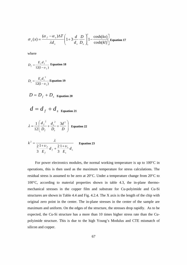
67
⎥⎦
⎤⎢⎣
⎡−⎟⎟
⎠
⎞⎜⎜⎝
⎛+
∆−=
)cosh()cosh(
131)(
)(klkx
DD
dd
dT
xsss
sfs λ
αασ Equation 17
where
)1(12
3
f
fff
dED
υ−= Equation 18
)1(12
3
s
sss
dED
υ−= Equation 19
sf DDD += Equation 20
sf ddd += Equation 21
⎟⎟⎠
⎞⎜⎜⎝
⎛++=
Dd
Dd
Dd
s
s
f
f222
3121λ Equation 22
ss
sf
f
f dE
dE
kυυ
λ+
++
=1
321
32
2 Equation 23
For power electronics modules, the normal working temperature is up to 100°C in
operations, this is then used as the maximum temperature for stress calculations. The
residual stress is assumed to be zero at 20°C. Under a temperature change from 20°C to
100°C, according to material properties shown in table 4.3, the in-plane thermo-
mechanical stresses in the copper film and substrate for Cu-polyimide and Cu-Si
structures are shown in Table 4.4 and Fig. 4.2.4. The X axis is the length of the chip with
original zero point in the center. The in-plane stresses in the center of the sample are
maximum and uniform. On the edges of the structure, the stresses drop rapidly. As to be
expected, the Cu-Si structure has a more than 10 times higher stress rate than the Cu-
polyimide structure. This is due to the high Young’s Modulus and CTE mismatch of
silicon and copper.
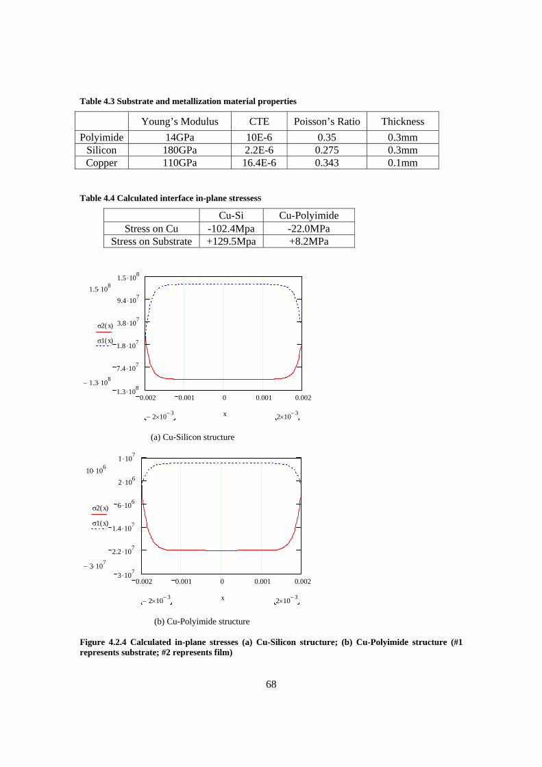
68
Table 4.3 Substrate and metallization material properties
Young’s Modulus CTE Poisson’s Ratio Thickness Polyimide 14GPa 10E-6 0.35 0.3mm
Silicon 180GPa 2.2E-6 0.275 0.3mm Copper 110GPa 16.4E-6 0.343 0.1mm
Table 4.4 Calculated interface in-plane stressesS
Cu-Si Cu-Polyimide Stress on Cu -102.4Mpa -22.0MPa
Stress on Substrate +129.5Mpa +8.2MPa
0.002 0.001 0 0.001 0.0021.3 .108
7.4 .107
1.8 .107
3.8 .107
9.4 .107
1.5 .108
1.5 108⋅
1.3− 108⋅
σ2 x( )
σ1 x( )
2 10 3−×2− 10 3−× x
(a) Cu-Silicon structure
0.002 0.001 0 0.001 0.0023 .107
2.2 .107
1.4 .107
6 .106
2 .106
1 .107
10 106⋅
3− 107⋅
σ2 x( )
σ1 x( )
2 10 3−×2− 10 3−× x
(b) Cu-Polyimide structure
Figure 4.2.4 Calculated in-plane stresses (a) Cu-Silicon structure; (b) Cu-Polyimide structure (#1 represents substrate; #2 represents film)
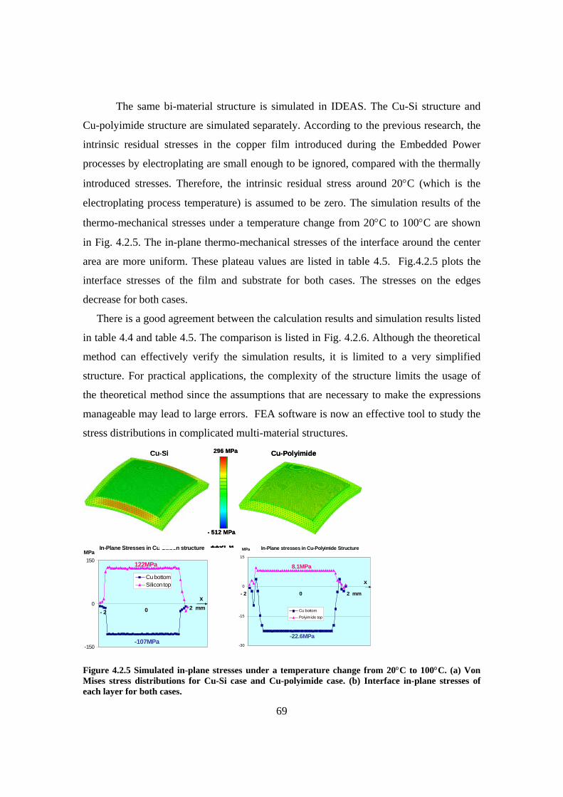
69
The same bi-material structure is simulated in IDEAS. The Cu-Si structure and
Cu-polyimide structure are simulated separately. According to the previous research, the
intrinsic residual stresses in the copper film introduced during the Embedded Power
processes by electroplating are small enough to be ignored, compared with the thermally
introduced stresses. Therefore, the intrinsic residual stress around 20°C (which is the
electroplating process temperature) is assumed to be zero. The simulation results of the
thermo-mechanical stresses under a temperature change from 20°C to 100°C are shown
in Fig. 4.2.5. The in-plane thermo-mechanical stresses of the interface around the center
area are more uniform. These plateau values are listed in table 4.5. Fig.4.2.5 plots the
interface stresses of the film and substrate for both cases. The stresses on the edges
decrease for both cases.
There is a good agreement between the calculation results and simulation results listed
in table 4.4 and table 4.5. The comparison is listed in Fig. 4.2.6. Although the theoretical
method can effectively verify the simulation results, it is limited to a very simplified
structure. For practical applications, the complexity of the structure limits the usage of
the theoretical method since the assumptions that are necessary to make the expressions
manageable may lead to large errors. FEA software is now an effective tool to study the
stress distributions in complicated multi-material structures. 296 MPa
- 512 MPa
Cu-Si Cu-Polyimide296 MPa
- 512 MPa
Cu-Si Cu-Polyimide
Figure 4.2.5 Simulated in-plane stresses under a temperature change from 20°C to 100°C. (a) Von Mises stress distributions for Cu-Si case and Cu-polyimide case. (b) Interface in-plane stresses of each layer for both cases.
119Pa119PaIn-Plane Stresses in Cu-Silicon structure
-150
0
150MPa
Cu bottomSilicon top
0 2 mm- 2
x
122MPa
-107MPa
In-Plane Stresses in Cu-Silicon structure
-150
0
150MPa
Cu bottomSilicon top
0 2 mm- 2
x
122MPa
-107MPa
In-Plane stresses in Cu-Polyimide Structure
-30
-15
0
15
MPa
Cu bottomPolyimide top
0 2 mm- 2
8.1MPa
-22.6MPa
x
In-Plane stresses in Cu-Polyimide Structure
-30
-15
0
15
MPa
Cu bottomPolyimide top
0 2 mm- 2
8.1MPa
-22.6MPa
x
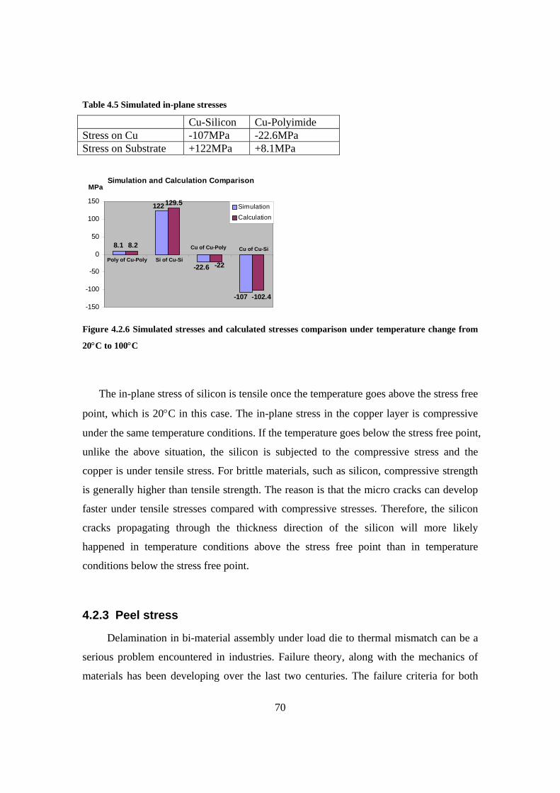
70
Table 4.5 Simulated in-plane stresses
Cu-Silicon Cu-Polyimide Stress on Cu -107MPa -22.6MPa Stress on Substrate +122MPa +8.1MPa
Simulation and Calculation Comparison
8.1
-22.6
-107
122
-102.4
129.5
8.2
-22
-150
-100
-50
0
50
100
150
MPa
SimulationCalculation
Poly of Cu-Poly Si of Cu-Si
Cu of Cu-Poly Cu of Cu-Si
Simulation and Calculation Comparison
8.1
-22.6
-107
122
-102.4
129.5
8.2
-22
-150
-100
-50
0
50
100
150
MPa
SimulationCalculation
Poly of Cu-Poly Si of Cu-Si
Cu of Cu-Poly Cu of Cu-Si
Figure 4.2.6 Simulated stresses and calculated stresses comparison under temperature change from
20°C to 100°C
The in-plane stress of silicon is tensile once the temperature goes above the stress free
point, which is 20°C in this case. The in-plane stress in the copper layer is compressive
under the same temperature conditions. If the temperature goes below the stress free point,
unlike the above situation, the silicon is subjected to the compressive stress and the
copper is under tensile stress. For brittle materials, such as silicon, compressive strength
is generally higher than tensile strength. The reason is that the micro cracks can develop
faster under tensile stresses compared with compressive stresses. Therefore, the silicon
cracks propagating through the thickness direction of the silicon will more likely
happened in temperature conditions above the stress free point than in temperature
conditions below the stress free point.
4.2.3 Peel stress
Delamination in bi-material assembly under load die to thermal mismatch can be a
serious problem encountered in industries. Failure theory, along with the mechanics of
materials has been developing over the last two centuries. The failure criteria for both

71
brittle and plastic homogeneous materials are well known. However, little is known about
interfacial failure, and what quantities to use as failure criteria. In literature, the shear
stress at the materials’ interface is cited as the failure indicator responsible for
delamination [62]. For a given biomaterial strip, the shear stress is only dependent on the
magnitude of the temperature difference. However, the peel stress is dependent on the
magnitude and sign of the temperature difference, as well as the mechanical and
geometrical parameters of the strips. It is speculated that normal interfacial stress plays a
significant role in delamination. [63]. Later experiments verify that there is close
relationship between the delamination and peel stress. We will address this issue later
where we introduce the power cycling tests. In this chapter, the peel stress is investigated
by calculation and simulation as the failure indicator of interfacial delamination.
In Suhir’s model, one drawback is that the peeling stress violates global equilibrium,
and the stress equilibrium in the direction normal to the layers is not satisfied unless an
additional concentrated force is introduced at the free edge. In Kang Ping Wang’s model,
this issue is addressed. A simple, but rather accurate expression of interfacial peeling
stress is obtained. Another improvement of Kang Ping Wang’s model is that the layers
don’t have to be the same length, as assumed in Suhir’s model. A simplified layer
structure is adopted. The thicknesses of the top and bottom are denoted by h1 and h2. The
thickness of the adhesive layer in between is ha, where ha<<h1, h2. The schematic of the
module cross-section is shown in Fig.4.2.7 [64].
Figure 4.2.7 Schematic of a bi-layer assembly with adhesion layer
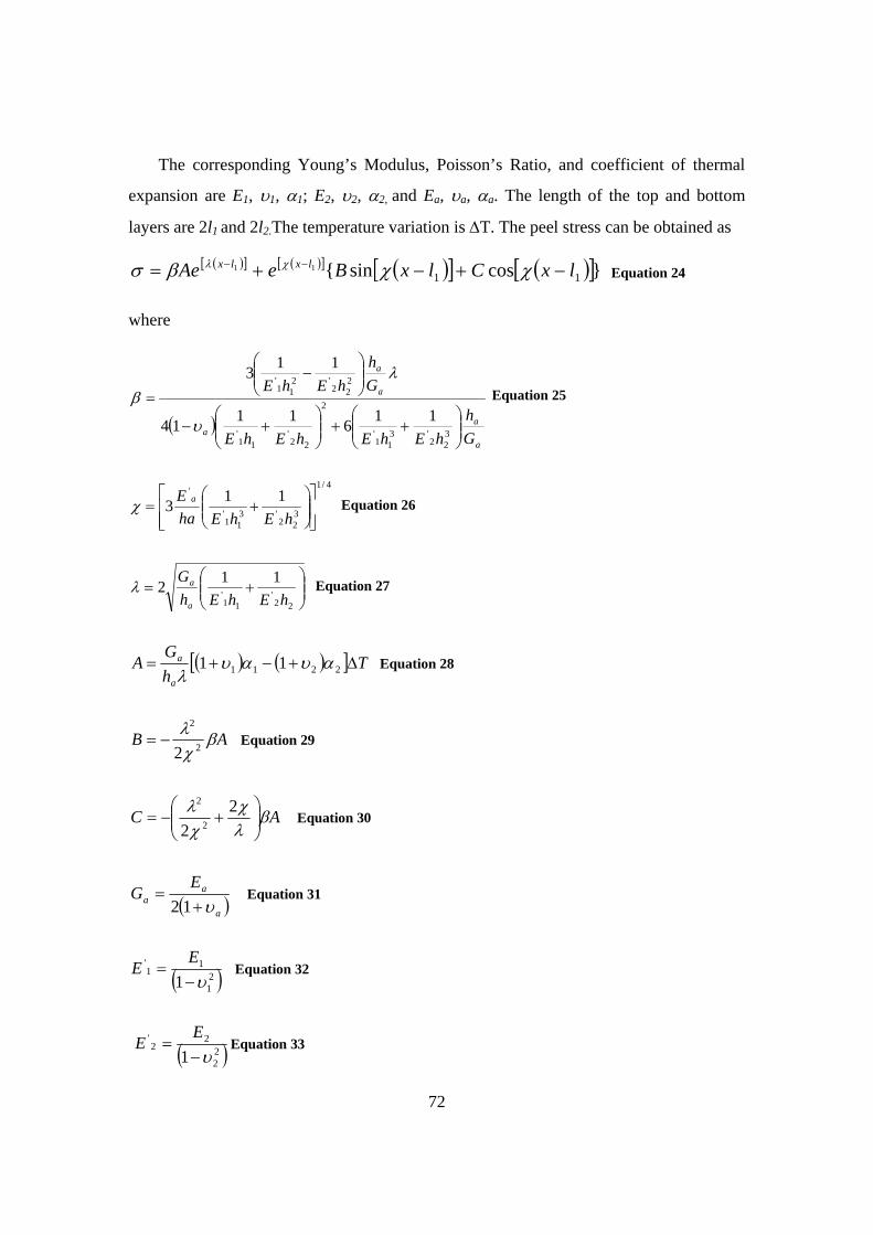
72
The corresponding Young’s Modulus, Poisson’s Ratio, and coefficient of thermal
expansion are E1, υ1, α1; E2, υ2, α2, and Ea, υa, αa. The length of the top and bottom
layers are 2l1 and 2l2.The temperature variation is ∆T. The peel stress can be obtained as
( )[ ] ( )[ ] ( )[ ] ( )[ ]cossin 1111 lxClxBeAe lxlx −+−+= −− χχβσ χλ
Equation 24
where
( )a
aa
a
a
Gh
hEhEhEhE
Gh
hEhE
⎟⎟⎠
⎞⎜⎜⎝
⎛++⎟⎟
⎠
⎞⎜⎜⎝
⎛+−
⎟⎟⎠
⎞⎜⎜⎝
⎛−
=
322
'311
'
2
22'
11'
222
'211
'
1161114
113
υ
λβ Equation 25
4/1
322
'311
'
' 113⎥⎥⎦
⎤
⎢⎢⎣
⎡⎟⎟⎠
⎞⎜⎜⎝
⎛+=
hEhEhaE aχ Equation 26
⎟⎟⎠
⎞⎜⎜⎝
⎛+=
22'
11'
112hEhEh
G
a
aλ Equation 27
( ) ( )[ ] ThG
Aa
a ∆+−+= 2211 11 αυαυλ
Equation 28
AB βχλ
2
2
2−= Equation 29
AC βλχ
χλ
⎟⎟⎠
⎞⎜⎜⎝
⎛+−=
22 2
2
Equation 30
( )a
aa
EG
υ+=
12 Equation 31
( )21
11'
1 υ−=
EE Equation 32
( )22
22
'
1 υ−=
EE Equation 33
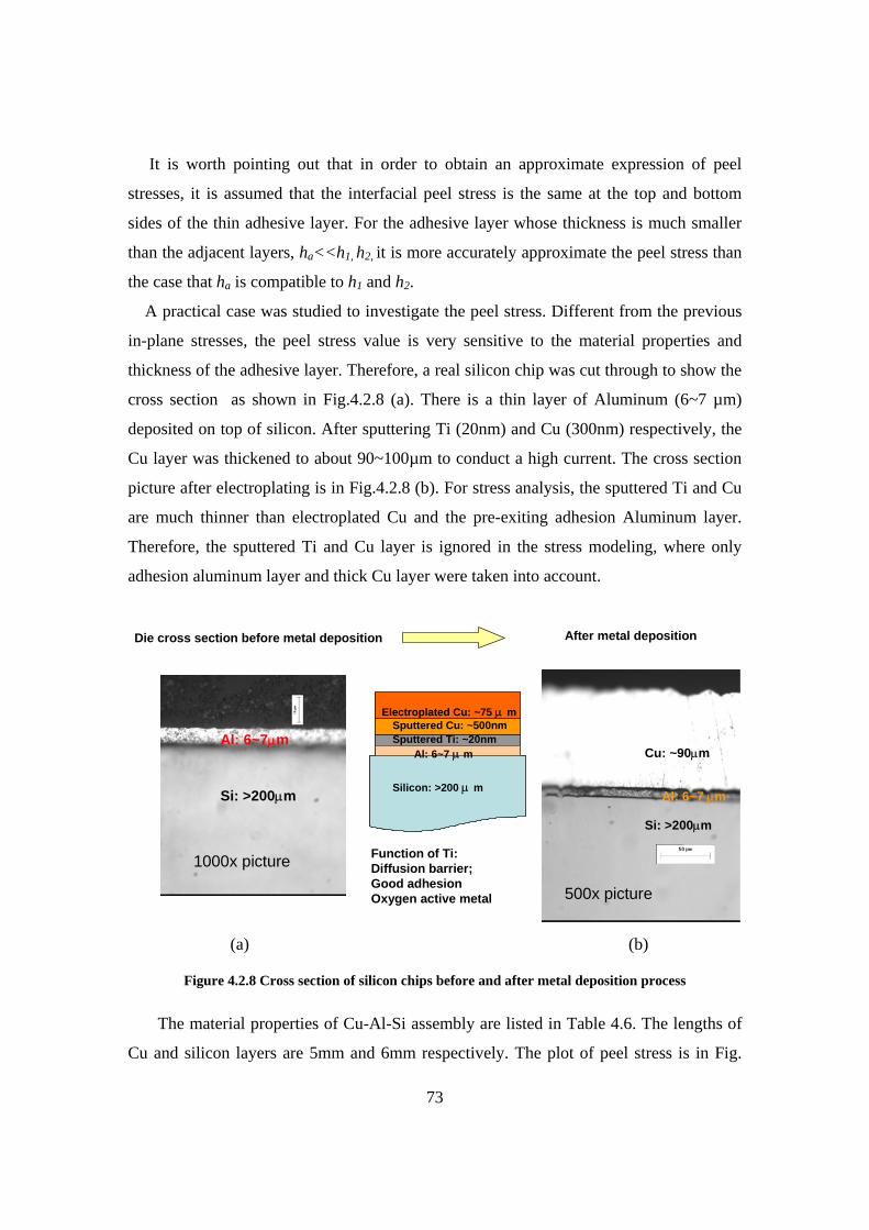
73
It is worth pointing out that in order to obtain an approximate expression of peel
stresses, it is assumed that the interfacial peel stress is the same at the top and bottom
sides of the thin adhesive layer. For the adhesive layer whose thickness is much smaller
than the adjacent layers, ha<<h1, h2, it is more accurately approximate the peel stress than
the case that ha is compatible to h1 and h2.
A practical case was studied to investigate the peel stress. Different from the previous
in-plane stresses, the peel stress value is very sensitive to the material properties and
thickness of the adhesive layer. Therefore, a real silicon chip was cut through to show the
cross section as shown in Fig.4.2.8 (a). There is a thin layer of Aluminum (6~7 µm)
deposited on top of silicon. After sputtering Ti (20nm) and Cu (300nm) respectively, the
Cu layer was thickened to about 90~100µm to conduct a high current. The cross section
picture after electroplating is in Fig.4.2.8 (b). For stress analysis, the sputtered Ti and Cu
are much thinner than electroplated Cu and the pre-exiting adhesion Aluminum layer.
Therefore, the sputtered Ti and Cu layer is ignored in the stress modeling, where only
adhesion aluminum layer and thick Cu layer were taken into account.
Die cross section before metal deposition
Al: 6~7µm
Si: >200µm
1000x picture
Al: 6~7µm
Si: >200µm
1000x picture
Cu: ~90µm
Al: 6~7 µm
Si: >200µm
Cu: ~90µm
Al: 6~7 µm
Si: >200µm
500x picture
Cu: ~90µm
Al: 6~7 µm
Si: >200µm
Cu: ~90µm
Al: 6~7 µm
Si: >200µm
500x picture
After metal deposition
Function of Ti:Diffusion barrier;Good adhesionOxygen active metal
Sputtered Ti: ~20nmSputtered Cu: ~500nm
Electroplated Cu: ~75 µ m
Silicon: >200 µ m
Al: 6~7 µ mSputtered Ti: ~20nmSputtered Cu: ~500nm
Electroplated Cu: ~75 µ m
Silicon: >200 µ m
Al: 6~7 µ m
(a) (b)
Figure 4.2.8 Cross section of silicon chips before and after metal deposition process
The material properties of Cu-Al-Si assembly are listed in Table 4.6. The lengths of
Cu and silicon layers are 5mm and 6mm respectively. The plot of peel stress is in Fig.
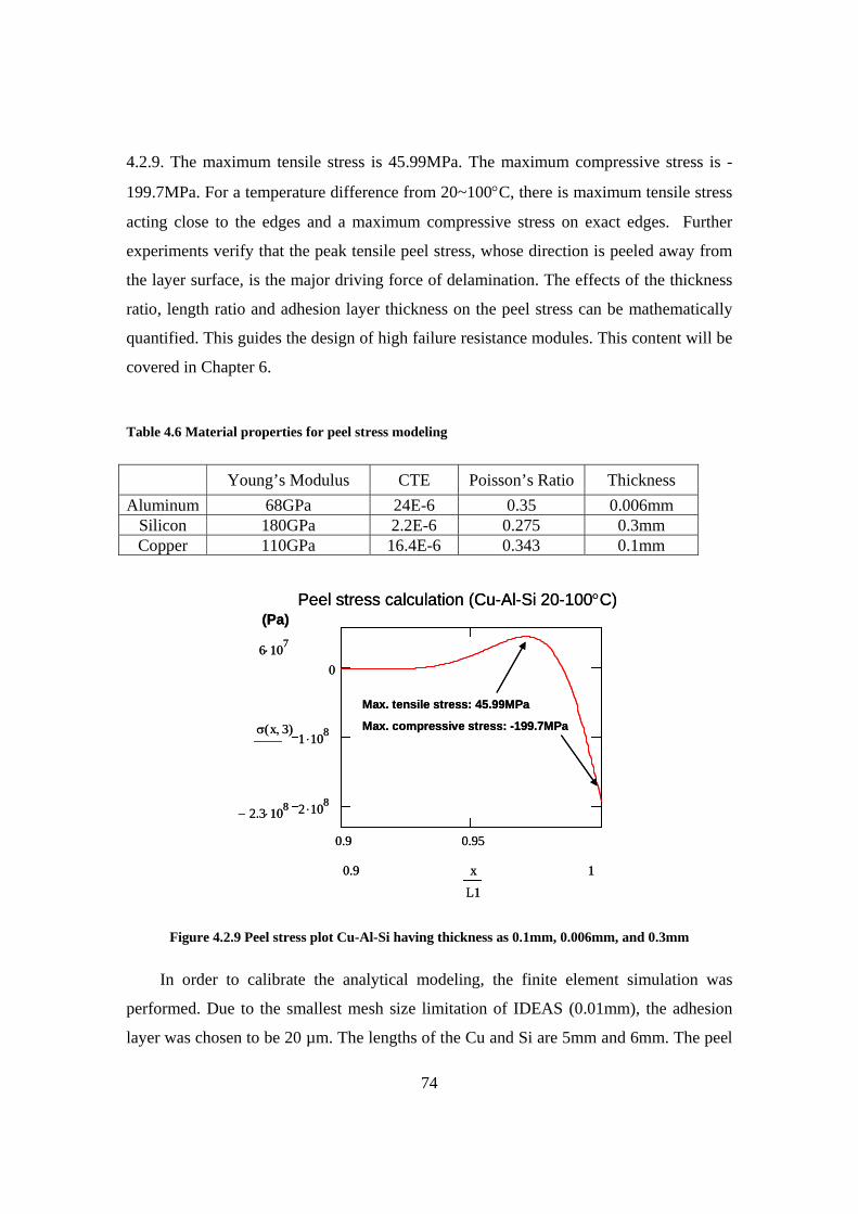
74
4.2.9. The maximum tensile stress is 45.99MPa. The maximum compressive stress is -
199.7MPa. For a temperature difference from 20~100°C, there is maximum tensile stress
acting close to the edges and a maximum compressive stress on exact edges. Further
experiments verify that the peak tensile peel stress, whose direction is peeled away from
the layer surface, is the major driving force of delamination. The effects of the thickness
ratio, length ratio and adhesion layer thickness on the peel stress can be mathematically
quantified. This guides the design of high failure resistance modules. This content will be
covered in Chapter 6.
Table 4.6 Material properties for peel stress modeling
Young’s Modulus CTE Poisson’s Ratio Thickness Aluminum 68GPa 24E-6 0.35 0.006mm
Silicon 180GPa 2.2E-6 0.275 0.3mm Copper 110GPa 16.4E-6 0.343 0.1mm
0.9 0.95
2 .108
1 .108
06 107⋅
2.3− 108⋅
σ x 3,( )
10.9 x
L1
Peel stress calculation (Cu-Al-Si 20-100°C)
Max. tensile stress: 45.99MPa
Max. compressive stress: -199.7MPa
(Pa)
0.9 0.95
2 .108
1 .108
06 107⋅
2.3− 108⋅
σ x 3,( )
10.9 x
L1
Peel stress calculation (Cu-Al-Si 20-100°C)
Max. tensile stress: 45.99MPa
Max. compressive stress: -199.7MPa
(Pa)
Figure 4.2.9 Peel stress plot Cu-Al-Si having thickness as 0.1mm, 0.006mm, and 0.3mm
In order to calibrate the analytical modeling, the finite element simulation was
performed. Due to the smallest mesh size limitation of IDEAS (0.01mm), the adhesion
layer was chosen to be 20 µm. The lengths of the Cu and Si are 5mm and 6mm. The peel
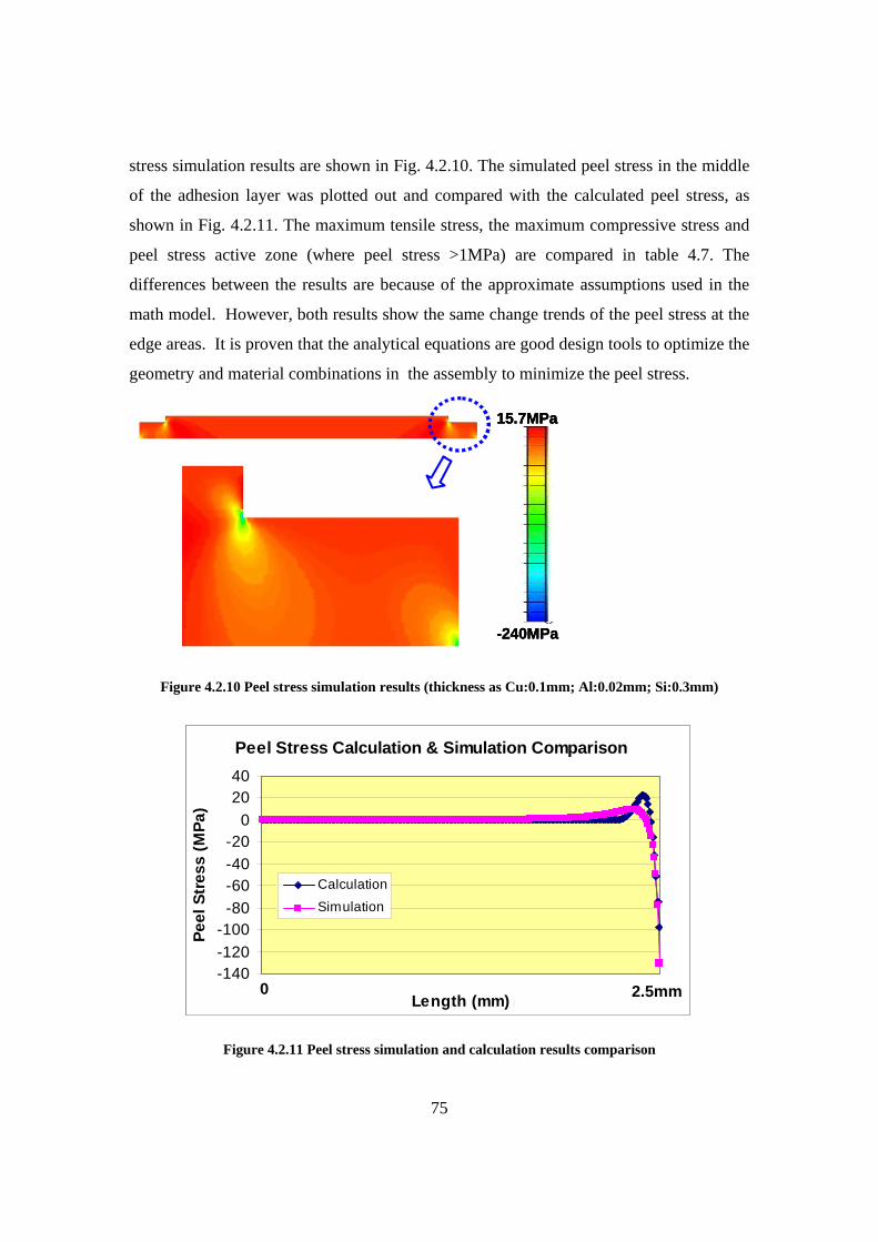
75
stress simulation results are shown in Fig. 4.2.10. The simulated peel stress in the middle
of the adhesion layer was plotted out and compared with the calculated peel stress, as
shown in Fig. 4.2.11. The maximum tensile stress, the maximum compressive stress and
peel stress active zone (where peel stress >1MPa) are compared in table 4.7. The
differences between the results are because of the approximate assumptions used in the
math model. However, both results show the same change trends of the peel stress at the
edge areas. It is proven that the analytical equations are good design tools to optimize the
geometry and material combinations in the assembly to minimize the peel stress.
15.7MPa
-240MPa
15.7MPa
-240MPa
15.7MPa
-240MPa
Figure 4.2.10 Peel stress simulation results (thickness as Cu:0.1mm; Al:0.02mm; Si:0.3mm)
Peel Stress Calculation & Simulation Comparison
-140-120-100
-80-60-40-20
02040
Length (mm)
Peel
Str
ess
(MPa
)
CalculationSimulation
2.5mm0
Peel Stress Calculation & Simulation Comparison
-140-120-100
-80-60-40-20
02040
Length (mm)
Peel
Str
ess
(MPa
)
CalculationSimulation
2.5mm0
Figure 4.2.11 Peel stress simulation and calculation results comparison
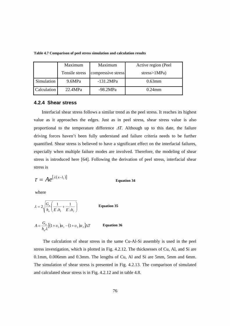
76
Table 4.7 Comparison of peel stress simulation and calculation results
Maximum
Tensile stress
Maximum
compressive stress
Active region (Peel
stress>1MPa)
Simulation 9.6MPa -131.2MPa 0.63mm
Calculation 22.4MPa -98.2MPa 0.24mm
4.2.4 Shear stress
Interfacial shear stress follows a similar trend as the peel stress. It reaches its highest
value as it approaches the edges. Just as in peel stress, shear stress value is also
proportional to the temperature difference ∆T. Although up to this date, the failure
driving forces haven’t been fully understand and failure criteria needs to be further
quantified. Shear stress is believed to have a significant effect on the interfacial failures,
especially when multiple failure modes are involved. Therefore, the modeling of shear
stress is introduced here [64]. Following the derivation of peel stress, interfacial shear
stress is
( )[ ]1lxAe −= λτ Equation 34
where
⎟⎟⎠
⎞⎜⎜⎝
⎛+=
22'
11'
112hEhEh
G
a
aλ Equation 35
( ) ( )[ ] ThG
Aa
a ∆+−+= 2211 11 αυαυλ
Equation 36
The calculation of shear stress in the same Cu-Al-Si assembly is used in the peel
stress investigation, which is plotted in Fig. 4.2.12. The thicknesses of Cu, Al, and Si are
0.1mm, 0.006mm and 0.3mm. The lengths of Cu, Al and Si are 5mm, 5mm and 6mm.
The simulation of shear stress is presented in Fig. 4.2.13. The comparison of simulated
and calculated shear stress is in Fig. 4.2.12 and in table 4.8.
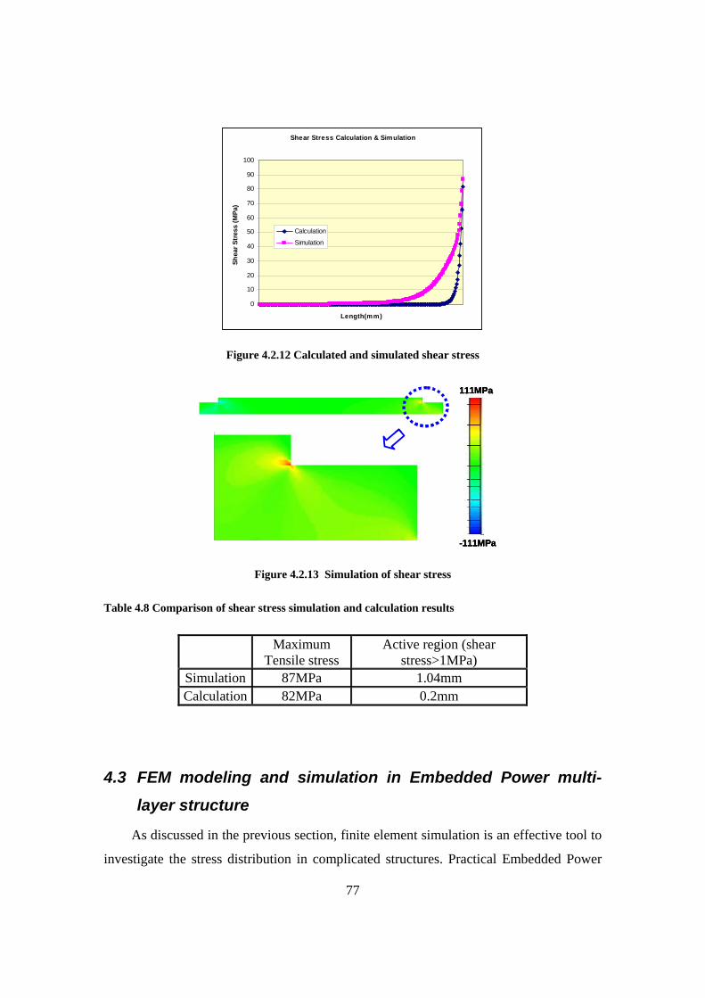
77
Shear Stress Calculation & Simulation
0
10
20
30
40
50
60
70
80
90
100
Length(mm)
Shea
r Str
ess
(MPa
)Calculation
Simulation
Figure 4.2.12 Calculated and simulated shear stress
111MPa
-111MPa
111MPa
-111MPa
111MPa
-111MPa
Figure 4.2.13 Simulation of shear stress
Table 4.8 Comparison of shear stress simulation and calculation results
Maximum Tensile stress
Active region (shear stress>1MPa)
Simulation 87MPa 1.04mm Calculation 82MPa 0.2mm
4.3 FEM modeling and simulation in Embedded Power multi-
layer structure
As discussed in the previous section, finite element simulation is an effective tool to
investigate the stress distribution in complicated structures. Practical Embedded Power
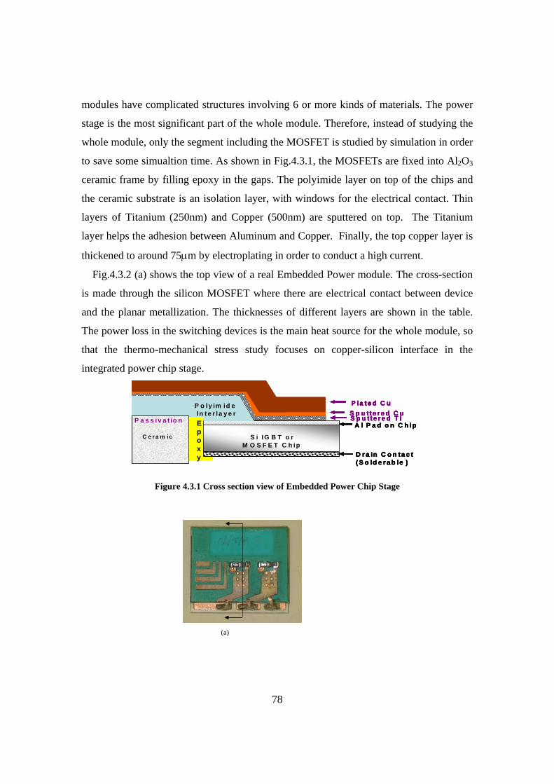
78
modules have complicated structures involving 6 or more kinds of materials. The power
stage is the most significant part of the whole module. Therefore, instead of studying the
whole module, only the segment including the MOSFET is studied by simulation in order
to save some simualtion time. As shown in Fig.4.3.1, the MOSFETs are fixed into Al2O3
ceramic frame by filling epoxy in the gaps. The polyimide layer on top of the chips and
the ceramic substrate is an isolation layer, with windows for the electrical contact. Thin
layers of Titanium (250nm) and Copper (500nm) are sputtered on top. The Titanium
layer helps the adhesion between Aluminum and Copper. Finally, the top copper layer is
thickened to around 75µm by electroplating in order to conduct a high current.
Fig.4.3.2 (a) shows the top view of a real Embedded Power module. The cross-section
is made through the silicon MOSFET where there are electrical contact between device
and the planar metallization. The thicknesses of different layers are shown in the table.
The power loss in the switching devices is the main heat source for the whole module, so
that the thermo-mechanical stress study focuses on copper-silicon interface in the
integrated power chip stage.
A l P a d o n C h ip
D r a in C o n ta c t( S o ld e r a b le )
S i IG B T o r M O S F E T C h ip
S p u t t e r e d T iS p u t t e r e d C uP la t e d C uP o ly im id e
In t e r la y e r
C e r a m ic
P a s s iv a t io nA l P a d o n C h ip
D r a in C o n ta c t( S o ld e r a b le )
S i IG B T o r M O S F E T C h ip
S p u t t e r e d T iS p u t t e r e d C uP la t e d C uP o ly im id e
In t e r la y e r
C e r a m ic
P a s s iv a t io n Epoxy
A l P a d o n C h ip
D r a in C o n ta c t( S o ld e r a b le )
S i IG B T o r M O S F E T C h ip
S p u t t e r e d T iS p u t t e r e d C uP la t e d C uP o ly im id e
In t e r la y e r
C e r a m ic
P a s s iv a t io nA l P a d o n C h ip
D r a in C o n ta c t( S o ld e r a b le )
S i IG B T o r M O S F E T C h ip
S p u t t e r e d T iS p u t t e r e d C uP la t e d C uP o ly im id e
In t e r la y e r
C e r a m ic
P a s s iv a t io nA l P a d o n C h ip
D r a in C o n ta c t( S o ld e r a b le )
S i IG B T o r M O S F E T C h ip
S p u t t e r e d T iS p u t t e r e d C uP la t e d C uP o ly im id e
In t e r la y e r
C e r a m ic
P a s s iv a t io nA l P a d o n C h ip
D r a in C o n ta c t( S o ld e r a b le )
S i IG B T o r M O S F E T C h ip
S p u t t e r e d T iS p u t t e r e d C uP la t e d C uP o ly im id e
In t e r la y e r
C e r a m ic
P a s s iv a t io n Epoxy
Figure 4.3.1 Cross section view of Embedded Power Chip Stage
(a)
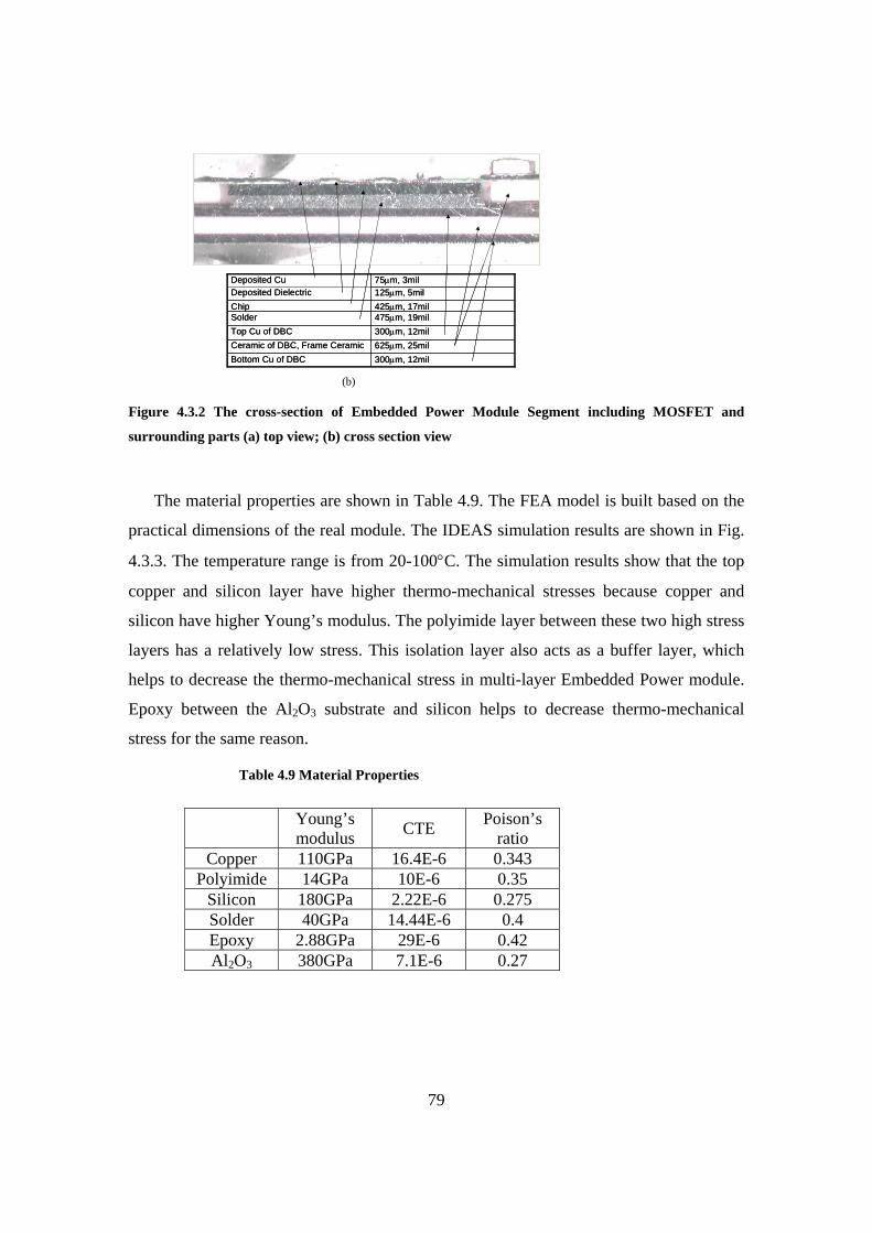
79
300µm, 12milBottom Cu of DBC625µm, 25milCeramic of DBC, Frame Ceramic300µm, 12milTop Cu of DBC475µm, 19milSolder425µm, 17milChip125µm, 5milDeposited Dielectric75µm, 3milDeposited Cu
300µm, 12milBottom Cu of DBC625µm, 25milCeramic of DBC, Frame Ceramic300µm, 12milTop Cu of DBC475µm, 19milSolder425µm, 17milChip125µm, 5milDeposited Dielectric75µm, 3milDeposited Cu
(b)
Figure 4.3.2 The cross-section of Embedded Power Module Segment including MOSFET and
surrounding parts (a) top view; (b) cross section view
The material properties are shown in Table 4.9. The FEA model is built based on the
practical dimensions of the real module. The IDEAS simulation results are shown in Fig.
4.3.3. The temperature range is from 20-100°C. The simulation results show that the top
copper and silicon layer have higher thermo-mechanical stresses because copper and
silicon have higher Young’s modulus. The polyimide layer between these two high stress
layers has a relatively low stress. This isolation layer also acts as a buffer layer, which
helps to decrease the thermo-mechanical stress in multi-layer Embedded Power module.
Epoxy between the Al2O3 substrate and silicon helps to decrease thermo-mechanical
stress for the same reason.
Table 4.9 Material Properties
Young’s modulus CTE Poison’s
ratio Copper 110GPa 16.4E-6 0.343
Polyimide 14GPa 10E-6 0.35 Silicon 180GPa 2.22E-6 0.275 Solder 40GPa 14.44E-6 0.4 Epoxy 2.88GPa 29E-6 0.42 Al2O3 380GPa 7.1E-6 0.27
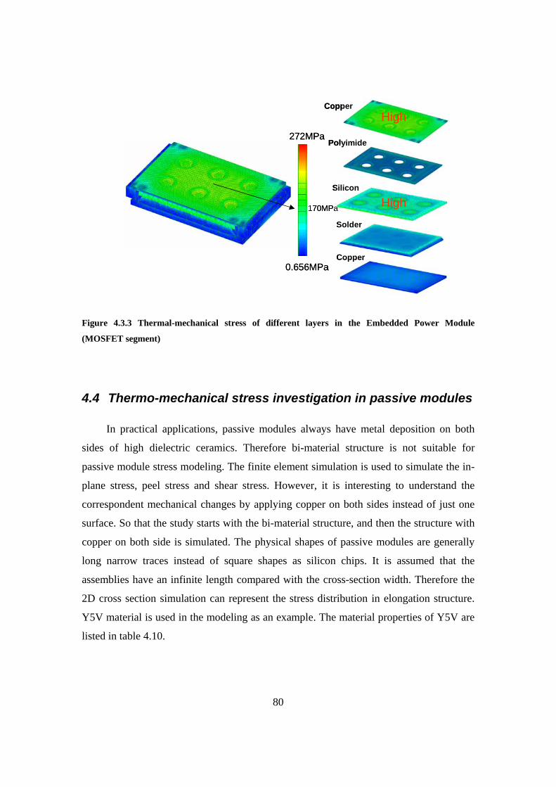
80
272MPa
0.656MPa
170MPa
High
High
Copper
Polyimide
Silicon
Solder
Copper
272MPa
0.656MPa
170MPa
High
High
Copper
Polyimide
Silicon
Solder
Copper
Figure 4.3.3 Thermal-mechanical stress of different layers in the Embedded Power Module
(MOSFET segment)
4.4 Thermo-mechanical stress investigation in passive modules
In practical applications, passive modules always have metal deposition on both
sides of high dielectric ceramics. Therefore bi-material structure is not suitable for
passive module stress modeling. The finite element simulation is used to simulate the in-
plane stress, peel stress and shear stress. However, it is interesting to understand the
correspondent mechanical changes by applying copper on both sides instead of just one
surface. So that the study starts with the bi-material structure, and then the structure with
copper on both side is simulated. The physical shapes of passive modules are generally
long narrow traces instead of square shapes as silicon chips. It is assumed that the
assemblies have an infinite length compared with the cross-section width. Therefore the
2D cross section simulation can represent the stress distribution in elongation structure.
Y5V material is used in the modeling as an example. The material properties of Y5V are
listed in table 4.10.
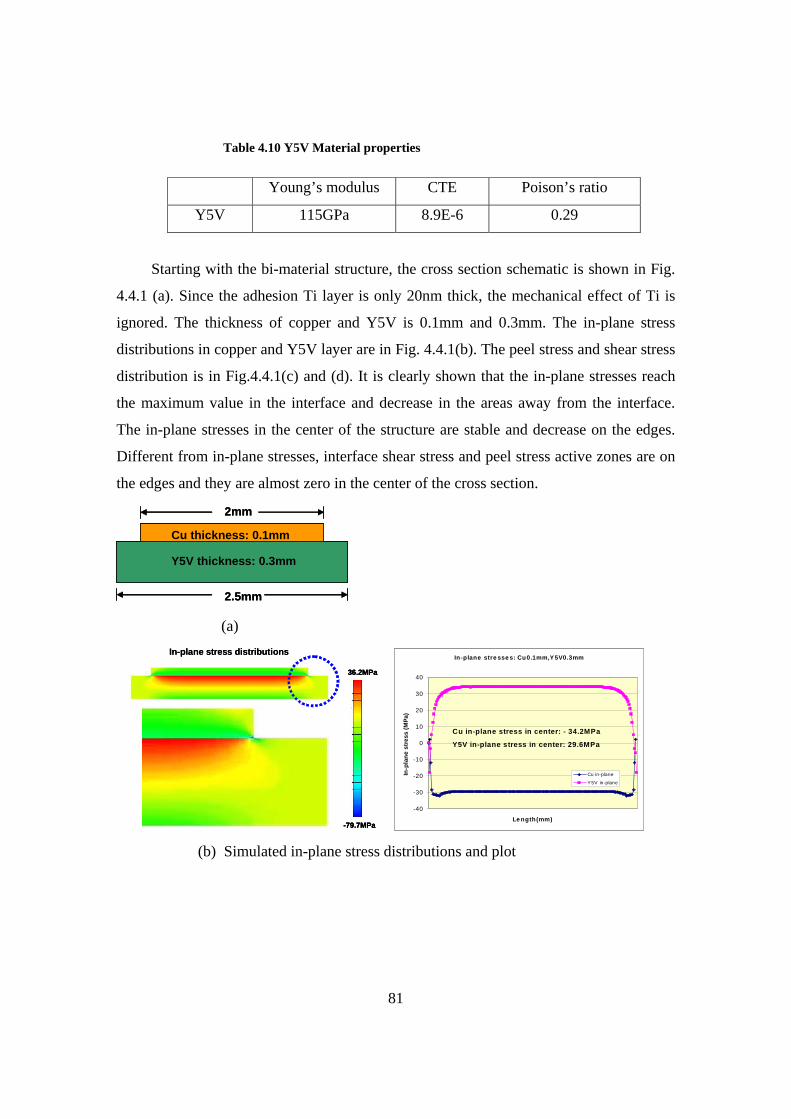
81
Table 4.10 Y5V Material properties
Young’s modulus CTE Poison’s ratio
Y5V 115GPa 8.9E-6 0.29
Starting with the bi-material structure, the cross section schematic is shown in Fig.
4.4.1 (a). Since the adhesion Ti layer is only 20nm thick, the mechanical effect of Ti is
ignored. The thickness of copper and Y5V is 0.1mm and 0.3mm. The in-plane stress
distributions in copper and Y5V layer are in Fig. 4.4.1(b). The peel stress and shear stress
distribution is in Fig.4.4.1(c) and (d). It is clearly shown that the in-plane stresses reach
the maximum value in the interface and decrease in the areas away from the interface.
The in-plane stresses in the center of the structure are stable and decrease on the edges.
Different from in-plane stresses, interface shear stress and peel stress active zones are on
the edges and they are almost zero in the center of the cross section.
Cu thickness: 0.1mm
Y5V thickness: 0.3mm
2mm
2.5mm
Cu thickness: 0.1mm
Y5V thickness: 0.3mm
2mm
2.5mm (a)
36.2MPa
-79.7MPa
In-plane stress distributions
36.2MPa
-79.7MPa
36.2MPa
-79.7MPa
In-plane stress distributionsIn-plane stre sse s: Cu0.1mm,Y5V0.3mm
-40
-30
-20
-10
0
10
20
30
40
Le ngth(mm)
In-p
lane
str
ess
(MPa
)
Cu in-plane
Y 5V in-plane
Cu in-plane stress in center: - 34.2MPa
Y5V in-plane stress in center: 29.6MPa
In-plane stre sse s: Cu0.1mm,Y5V0.3mm
-40
-30
-20
-10
0
10
20
30
40
Le ngth(mm)
In-p
lane
str
ess
(MPa
)
Cu in-plane
Y 5V in-plane
Cu in-plane stress in center: - 34.2MPa
Y5V in-plane stress in center: 29.6MPa
(b) Simulated in-plane stress distributions and plot
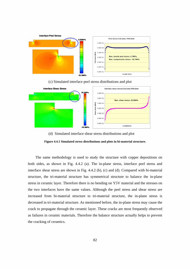
82
9.83MPa
-51.9MPa
Interface Peel Stress9.83MPa
-51.9MPa
Interface Peel Stress
Peel stress Cu0.1mm, Y5V0.3mm
-5.00E+01
-4.00E+01
-3.00E+01
-2.00E+01
-1.00E+01
0.00E+00
1.00E+01
Length (mm)
Pee
l str
ess
(MP
a)
Max. tensile peel stress: 2.7MPa
Max. compressive stress: -43.7MPa
Peel stress Cu0.1mm, Y5V0.3mm
-5.00E+01
-4.00E+01
-3.00E+01
-2.00E+01
-1.00E+01
0.00E+00
1.00E+01
Length (mm)
Pee
l str
ess
(MP
a)
Max. tensile peel stress: 2.7MPa
Max. compressive stress: -43.7MPa
(c) Simulated interface peel stress distributions and plot
30.3MPa
-30.3MPa
Interface Shear Stress30.3MPa
-30.3MPa
Interface Shear Stress Interface shear stress:Cu0.1mm,Y5V0.3mm
-3.00E+01
-2.00E+01
-1.00E+01
0.00E+00
1.00E+01
2.00E+01
3.00E+01
Length(mm)
Shea
r st
ress
(MPa
)
Max. shear stress: 22.9MPa
Interface shear stress:Cu0.1mm,Y5V0.3mm
-3.00E+01
-2.00E+01
-1.00E+01
0.00E+00
1.00E+01
2.00E+01
3.00E+01
Length(mm)
Shea
r st
ress
(MPa
)
Max. shear stress: 22.9MPa
(d) Simulated interface shear stress distributions and plot
Figure 4.4.1 Simulated stress distributions and plots in bi-material structure.
The same methodology is used to study the structure with copper depositions on
both sides, as shown in Fig. 4.4.2 (a). The in-plane stress, interface peel stress and
interface shear stress are shown in Fig. 4.4.2 (b), (c) and (d). Compared with bi-material
structure, the tri-material structure has symmetrical structure to balance the in-plane
stress in ceramic layer. Therefore there is no bending on Y5V material and the stresses on
the two interfaces have the same values. Although the peel stress and shear stress are
increased from bi-material structure to tri-material structure, the in-plane stress is
decreased in tri-material structure. As mentioned before, the in-plane stress may cause the
crack to propagate through the ceramic layer. These cracks are most frequently observed
as failures in ceramic materials. Therefore the balance structure actually helps to prevent
the cracking of ceramics.

83
Cu thickness: 0.1mm
Y5V thickness: 0.3mm
2mm
2.5mmCu thickness: 0.1mm
2mm
Cu thickness: 0.1mm
Y5V thickness: 0.3mm
2mm
2.5mmCu thickness: 0.1mm
2mm (a) Tri-material structure schematic
28.4MPa
-112 MPa
In-plane stress distributions 28.4MPa
-112 MPa
28.4MPa
-112 MPa
In-plane stress distributions
In-Plane Stresses:Cu0.1mm-Y5V0.3mm-Cu0.1mm
-5.00E+01
-4.00E+01
-3.00E+01
-2.00E+01
-1.00E+01
0.00E+00
1.00E+01
2.00E+01
3.00E+01
4.00E+01
Length (mm)
In-p
lan
e st
ress
(M
P
Cu in-planeY5V in-plane
Cu in-plane stress in center: - 40.3MPaY5V in-plane stress in center: 26.9 MPa
In-Plane Stresses:Cu0.1mm-Y5V0.3mm-Cu0.1mm
-5.00E+01
-4.00E+01
-3.00E+01
-2.00E+01
-1.00E+01
0.00E+00
1.00E+01
2.00E+01
3.00E+01
4.00E+01
Length (mm)
In-p
lan
e st
ress
(M
P
Cu in-planeY5V in-plane
Cu in-plane stress in center: - 40.3MPaY5V in-plane stress in center: 26.9 MPa
(b) Tri-material structure in-plane stress distributions and plots
7.45MPa
- 81.0MPa
Interface Peel Stress Distributions7.45MPa
- 81.0MPa
7.45MPa
- 81.0MPa
Interface Peel Stress Distributions
Interface Peel Stress: Cu0.1mm-Y5V0.3mm-Cu0.1mm
-7.00E+01
-6.00E+01
-5.00E+01
-4.00E+01
-3.00E+01
-2.00E+01
-1.00E+01
0.00E+00
1.00E+01
Length(mm)
Peel
str
ess
(MPa
)
Max. tensile peel stress: 3.89 MPaMax. compressive stress: - 65.3 MPa
Interface Peel Stress: Cu0.1mm-Y5V0.3mm-Cu0.1mm
-7.00E+01
-6.00E+01
-5.00E+01
-4.00E+01
-3.00E+01
-2.00E+01
-1.00E+01
0.00E+00
1.00E+01
Length(mm)
Peel
str
ess
(MPa
)
Max. tensile peel stress: 3.89 MPaMax. compressive stress: - 65.3 MPa
(c) Tri-material structure peel stress distribution and plot
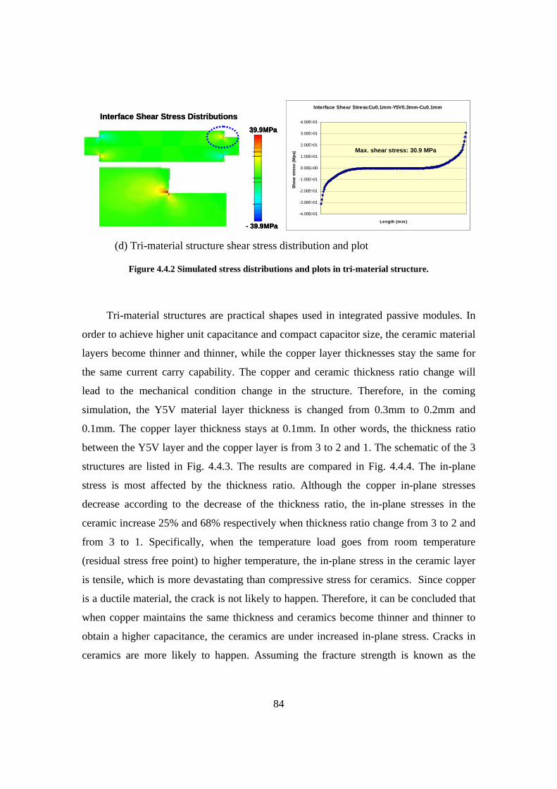
84
39.9MPa
- 39.9MPa
Interface Shear Stress Distributions39.9MPa
- 39.9MPa
39.9MPa
- 39.9MPa
Interface Shear Stress Distributions
Interface Shear Stress:Cu0.1mm-Y5V0.3mm-Cu0.1mm
-4.00E+01
-3.00E+01
-2.00E+01
-1.00E+01
0.00E+00
1.00E+01
2.00E+01
3.00E+01
4.00E+01
Length (mm)
Shea
r str
ess
(Mpa
) Max. shear stress: 30.9 MPa
Interface Shear Stress:Cu0.1mm-Y5V0.3mm-Cu0.1mm
-4.00E+01
-3.00E+01
-2.00E+01
-1.00E+01
0.00E+00
1.00E+01
2.00E+01
3.00E+01
4.00E+01
Length (mm)
Shea
r str
ess
(Mpa
) Max. shear stress: 30.9 MPa
(d) Tri-material structure shear stress distribution and plot
Figure 4.4.2 Simulated stress distributions and plots in tri-material structure.
Tri-material structures are practical shapes used in integrated passive modules. In
order to achieve higher unit capacitance and compact capacitor size, the ceramic material
layers become thinner and thinner, while the copper layer thicknesses stay the same for
the same current carry capability. The copper and ceramic thickness ratio change will
lead to the mechanical condition change in the structure. Therefore, in the coming
simulation, the Y5V material layer thickness is changed from 0.3mm to 0.2mm and
0.1mm. The copper layer thickness stays at 0.1mm. In other words, the thickness ratio
between the Y5V layer and the copper layer is from 3 to 2 and 1. The schematic of the 3
structures are listed in Fig. 4.4.3. The results are compared in Fig. 4.4.4. The in-plane
stress is most affected by the thickness ratio. Although the copper in-plane stresses
decrease according to the decrease of the thickness ratio, the in-plane stresses in the
ceramic increase 25% and 68% respectively when thickness ratio change from 3 to 2 and
from 3 to 1. Specifically, when the temperature load goes from room temperature
(residual stress free point) to higher temperature, the in-plane stress in the ceramic layer
is tensile, which is more devastating than compressive stress for ceramics. Since copper
is a ductile material, the crack is not likely to happen. Therefore, it can be concluded that
when copper maintains the same thickness and ceramics become thinner and thinner to
obtain a higher capacitance, the ceramics are under increased in-plane stress. Cracks in
ceramics are more likely to happen. Assuming the fracture strength is known as the
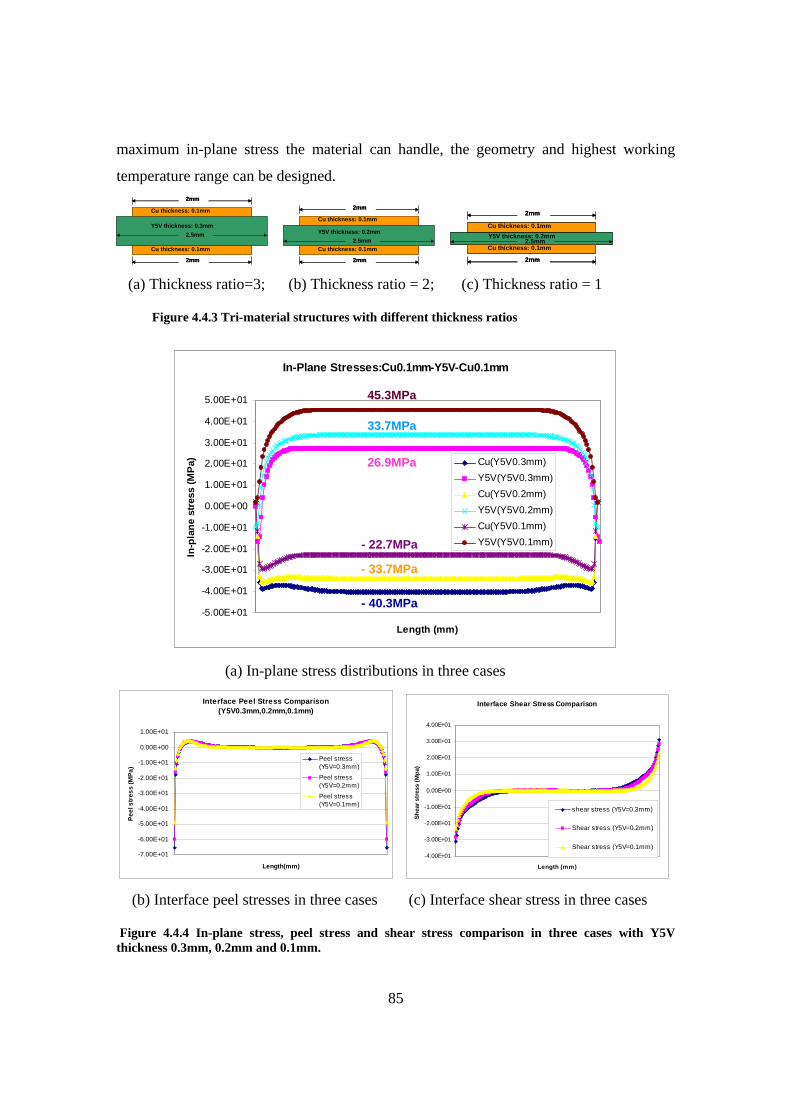
85
maximum in-plane stress the material can handle, the geometry and highest working
temperature range can be designed.
Cu thickness: 0.1mm
Y5V thickness: 0.3mm
2mm
2.5mm
Cu thickness: 0.1mm
2mm
Cu thickness: 0.1mm
Y5V thickness: 0.3mm
2mm
2.5mm
Cu thickness: 0.1mm
2mm
Cu thickness: 0.1mm
Y5V thickness: 0.2mm
2mm
2.5mmCu thickness: 0.1mm
2mm
Cu thickness: 0.1mm
Y5V thickness: 0.2mm
2mm
2.5mmCu thickness: 0.1mm
2mm
Cu thickness: 0.1mmY5V thickness: 0.2mm
2mm
2.5mmCu thickness: 0.1mm
2mm
Cu thickness: 0.1mmY5V thickness: 0.2mm
2mm
2.5mmCu thickness: 0.1mm
2mm (a) Thickness ratio=3; (b) Thickness ratio = 2; (c) Thickness ratio = 1
Figure 4.4.3 Tri-material structures with different thickness ratios
In-Plane Stresses:Cu0.1mm-Y5V-Cu0.1mm
-5.00E+01
-4.00E+01
-3.00E+01
-2.00E+01
-1.00E+01
0.00E+00
1.00E+01
2.00E+01
3.00E+01
4.00E+01
5.00E+01
Length (mm)
In-p
lane
stre
ss (M
Pa) Cu(Y5V0.3mm)
Y5V(Y5V0.3mm)Cu(Y5V0.2mm)Y5V(Y5V0.2mm)Cu(Y5V0.1mm)Y5V(Y5V0.1mm)
26.9MPa
33.7MPa
45.3MPa
- 40.3MPa
- 33.7MPa
- 22.7MPa
(a) In-plane stress distributions in three cases
Interface Peel Stress Comparison (Y5V0.3mm,0.2mm,0.1mm)
-7.00E+01
-6.00E+01
-5.00E+01
-4.00E+01
-3.00E+01
-2.00E+01
-1.00E+01
0.00E+00
1.00E+01
Length(mm)
Peel
str
ess
(MPa
)
Peel stress(Y5V=0.3mm)Peel stress(Y5V=0.2mm)
Peel stress(Y5V=0.1mm)
Interface Shear Stress Comparison
-4.00E+01
-3.00E+01
-2.00E+01
-1.00E+01
0.00E+00
1.00E+01
2.00E+01
3.00E+01
4.00E+01
Length (mm)
Shea
r str
ess
(Mpa
)
shear stress (Y5V=0.3mm)
Shear stress (Y5V=0.2mm)
Shear stress (Y5V=0.1mm)
(b) Interface peel stresses in three cases (c) Interface shear stress in three cases
Figure 4.4.4 In-plane stress, peel stress and shear stress comparison in three cases with Y5V thickness 0.3mm, 0.2mm and 0.1mm.
86
4.5 Chapter Review
In chapter 4, the thermal-mechanical stresses are investigated in integrated active
modules and integrated passive modules respectively. A bi-material structure with an
adhesive layer is utilized to simulate stress distributions in Active IPEMs, where only one
side of silicon has copper deposition. A tri-material structure is suitable for Passive
IPEMs because there are always copper layers on both sides of ceramic substrates. Von
Mises stress, in-plane stress, peel stress and shear stress are modeled as failure indicators
for metal fracture, substrate cracks, delamination and spalling. Von Mises stress theory is
based on the distortion energy theory. If Von Mises stress is greater than metal yield
stress, the metal fracture is likely to happen. However, in normal working temperatures,
the Von Mises stress in copper layer is typically less than 300MPa, which is the yield
stress of electroplated copper. Therefore, copper fracture is never found in failed samples.
In-plane stress is the failure indicator for ceramic cracks, especially when ceramics are
under tensile in-plane stress. In most of cases, temperatures above residual stress free
point will lead to compressive in-plane stress in metal and tensile in-plane stress in
substrate. Therefore, substrate cracks are the typical failure mode for samples working
under temperatures higher than stress free point. Tensile peel stress close to edges is the
failure indicator of delamination under temperature changes from stress free point to
higher ones. For temperature changes from stress free point to lower ones, the maximum
tensile peel stress exactly on edges will lead to substrate spalling, which starts at edges
and propagates parallel to the surface. Since peel stress includes more geometry and
material factors than shear stress, peel stress is given more attentions in this study than
shear stress.
The analytical modeling and finite element simulation are the methodologies used in
this chapter. The results are compared. Both results show the same trends according to
geometry or material changes. This proves that the analytical modeling are a good design
tool to optimize the geometry and material combinations. However, FEM simulation is an
effective tool to study complicated structures. Once the final selection has been made by
analytical model, FEM simulation can be used to verify and modify the design. The

87
simulations for complicated Embedded Power modules and integrated passive modules
indicate that the copper-silicon and copper-ceramic interfaces are the high stress spots.
Modeling provides insight into behaviors of the system. Modeled stresses must be
correlated with observed failures to be useful as failure indicators. In order to verify the
simulation results, the power cycling and temperature cycling tests are designed and
carried out for integrated power modules.
88
Chapter 5: Power Cycling and Temperature Cycling Test
Power cycling and temperature cycling test are the commonly used methods to test
the lifetime of the samples. According to the thermal mechanical stress simulation in the
multi layer structure, the higher stress is focus on the interface of the two materials,
which have high Young’s modulus, such as copper-silicon interface or copper-ceramic
interface. The test samples are prepared for the power cycling and temperature test.
Instead of having all the layers and materials use in the Embedded Power module, the test
samples have only a copper deposition on top of the silicon die fixed into the ceramic
substrate or on top of the ceramic substrate in the power passive modules.
5.1 Embedded Power modules power cycling test
5.1.1 Sample preparation
The failure modes of planar integrated passive modules under temperature cycling
have been presented in previous research. However, no work has yet been undertaken to
investigate the possible failure modes of the Embedded Power technology. The
Embedded power module has a multi layer structure. The test samples focus the study on
the silicon copper interface. The same manufacturing process used in Embedded Power
technology is used in the sample preparation.
As shown in Fig.5.1.1, the opening in a ceramic substrate is cut as the designed
pattern by laser machining. MOSFET chips are mounted into the holes of the Alumina
substrate. Epoxy is used as the gap filler between the MOSFET and ceramic substrate as
shown in Fig.5.1.1 (b). Since epoxy does not form a smooth surface, a solder mask layer
is applied to cover the epoxy and ceramic. The MOSFET, however is left as is, this is
shown in Fig. 5.1.1 (c). Titanium and copper are subsequently sputtered onto the sample
about 20nm and 500nm thick respectively. The copper on top of the silicon and the
necessary electrical contact patterns are thickened by electroplating the sample. A photo
resist layer as shown in Fig.5.1.1 (e) defines the copper pattern. The electroplating
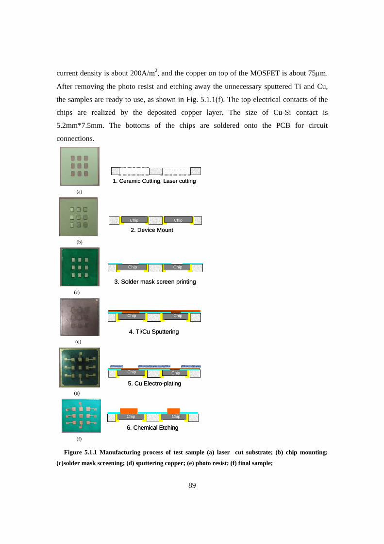
89
current density is about 200A/m2, and the copper on top of the MOSFET is about 75µm.
After removing the photo resist and etching away the unnecessary sputtered Ti and Cu,
the samples are ready to use, as shown in Fig. 5.1.1(f). The top electrical contacts of the
chips are realized by the deposited copper layer. The size of Cu-Si contact is
5.2mm*7.5mm. The bottoms of the chips are soldered onto the PCB for circuit
connections.
1. Ceramic Cutting, Laser cutting1. Ceramic Cutting, Laser cutting (a)
ChipChip
2. Device Mount
ChipChip
2. Device Mount
(b)
Chip Chip
3. Solder mask screen printing
Chip Chip
3. Solder mask screen printing (c)
4. Ti/Cu Sputtering
Chip Chip
4. Ti/Cu Sputtering
Chip Chip
(d)
Chip
5. Cu Electro-plating
ChipChip
5. Cu Electro-plating
Chip
(e)
Chip Chip
6. Chemical Etching
Chip Chip
6. Chemical Etching
(f)
Figure 5.1.1 Manufacturing process of test sample (a) laser cut substrate; (b) chip mounting;
(c)solder mask screening; (d) sputtering copper; (e) photo resist; (f) final sample;

90
5.1.2 Power cycling test setup and test results
According to literature [65], the thin films under tensile and compressive stresses
have different failure modes. The commonly observed fracture patterns in pre-tensioned
films include surface cracking, channeling, substrate damage, substrate spalling and film
debonding. Due to the material properties of the ductile copper film and brittle substrates,
the substrate damage, substrate spalling or film debonding are possible failure modes in
the IPEMs.
The improved power-cycling test has cycling time control and temperature feedback
control. The schematic of the test circuit is shown in Fig.5.1.2. The test samples are
placed inside the TenneyTM temperature chamber to provide constant environment
temperatures. A power supply works as a current source and supplies the constant current
through the diodes. The current and the voltage drops on the diodes cause the temperature
to rise up in the diode. The heating up speed can be controlled by the values of the
supplied current. The samples were cooled down while the current was cut off. The
cycling time is controlled by a timer. During current on time, the temperature feedback
prevents the sample temperature beyond the designed maximum temperature. The sample
temperatures were sensed by thermal couples attached on top of the copper. In order to
separate the driving forces for different failure modes, two temperature profiles were
used as shown in Fig. 5.1.3. One is from 25°C, which is the intrinsic residual stress free
point, to 125°C. Under this temperature profile, the copper film is in compressive stress
and the substrate is under tensile stress. The preliminary test results showed that the
sample had a long lifetime up to 15480 cycles. In order to accelerate the failures, the
temperature profile from 25°C to 175°C (high temperature profile) was used. The other
temperature profile was from room temperature to -75°C (low temperature profile). In
this case, the film is under tensile stress and the substrate is under compressive stress.
The power cycling test results are summarized in Fig.5.1.3. One sample survived
15480 cycles under temperature from 25°C to 125°. The other 4 samples were under
temperatures ranging from 25°C to 175°C. The samples failed after 335, 340, 1245 and
1250 cycles respectively. 3 samples were under temperature change from -75°C to 25°C.
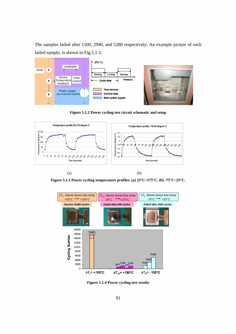
91
The samples failed after 1500, 2940, and 5280 respectively. An example picture of each
failed sample, is shown in Fig.5.1.3.
controller
DeviceTemperature
feedback
Timercontrol
Power supply as a current source
diode
Test devicesControl loopMain power supply
Test devicesControl loopMain power supply
Heating Cooling Heating
∆T( °C)
Time(sec)Cycle time
Heating Cooling Heating
∆T( °C)
Time(sec)Cycle time
Figure 5.1.2 Power cycling test circuit schematic and setup
Temperature profile 25-175 degree C
0
50
100
150
200
0 15 30 45 60 75 90105
120135
150165
180
195210
225
240
Time (seconds)
Tem
pera
ture
(deg
ree
C)
Temperature profile -75-25 degree C
-80
-60
-40
-20
0
20
40
0 15 30 45 60 75 90105 120 135 150 165 180 195 210 225 240
Time (second)
Tem
pera
ture
(deg
ree
C)
(a) (b)
Figure 5.1.3 Power cycling temperature profiles. (a) 25°C~175°C. (b) -75°C~25°C.
∆T1: Above stress free temp.
+25°C +125°C∆T1: Above stress free temp.
+25°C +125°C∆T2: Below stress free temp.
-75°C +25°C∆T2: Below stress free temp.
-75°C +25°C∆T12: Above stress free temp.
25°C +175°C∆T12: Above stress free temp.
25°C +175°C
Survive 15480 cycles Failed after 840 cycles Failed after 1500 cycles
Figure 5.1.4 Power cycling test results
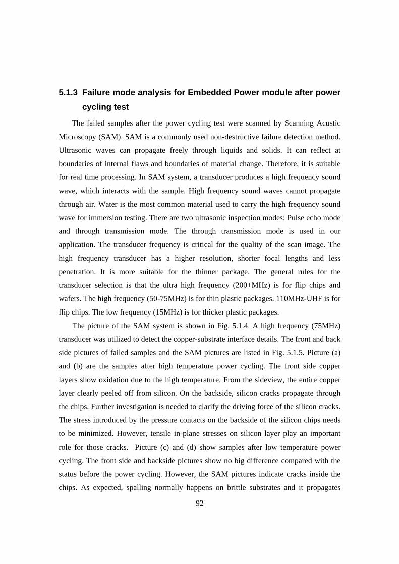
92
5.1.3 Failure mode analysis for Embedded Power module after power cycling test
The failed samples after the power cycling test were scanned by Scanning Acustic
Microscopy (SAM). SAM is a commonly used non-destructive failure detection method.
Ultrasonic waves can propagate freely through liquids and solids. It can reflect at
boundaries of internal flaws and boundaries of material change. Therefore, it is suitable
for real time processing. In SAM system, a transducer produces a high frequency sound
wave, which interacts with the sample. High frequency sound waves cannot propagate
through air. Water is the most common material used to carry the high frequency sound
wave for immersion testing. There are two ultrasonic inspection modes: Pulse echo mode
and through transmission mode. The through transmission mode is used in our
application. The transducer frequency is critical for the quality of the scan image. The
high frequency transducer has a higher resolution, shorter focal lengths and less
penetration. It is more suitable for the thinner package. The general rules for the
transducer selection is that the ultra high frequency (200+MHz) is for flip chips and
wafers. The high frequency (50-75MHz) is for thin plastic packages. 110MHz-UHF is for
flip chips. The low frequency (15MHz) is for thicker plastic packages.
The picture of the SAM system is shown in Fig. 5.1.4. A high frequency (75MHz)
transducer was utilized to detect the copper-substrate interface details. The front and back
side pictures of failed samples and the SAM pictures are listed in Fig. 5.1.5. Picture (a)
and (b) are the samples after high temperature power cycling. The front side copper
layers show oxidation due to the high temperature. From the sideview, the entire copper
layer clearly peeled off from silicon. On the backside, silicon cracks propagate through
the chips. Further investigation is needed to clarify the driving force of the silicon cracks.
The stress introduced by the pressure contacts on the backside of the silicon chips needs
to be minimized. However, tensile in-plane stresses on silicon layer play an important
role for those cracks. Picture (c) and (d) show samples after low temperature power
cycling. The front side and backside pictures show no big difference compared with the
status before the power cycling. However, the SAM pictures indicate cracks inside the
chips. As expected, spalling normally happens on brittle substrates and it propagates
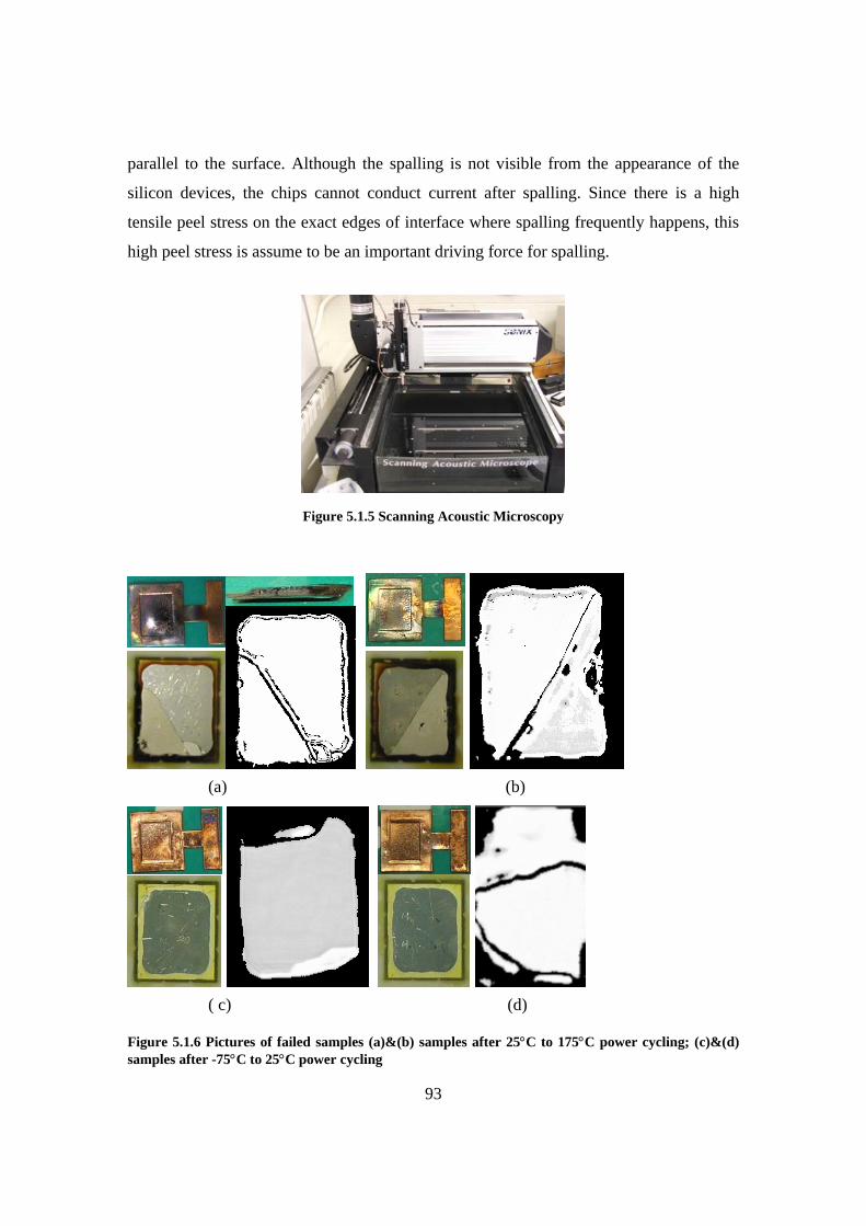
93
parallel to the surface. Although the spalling is not visible from the appearance of the
silicon devices, the chips cannot conduct current after spalling. Since there is a high
tensile peel stress on the exact edges of interface where spalling frequently happens, this
high peel stress is assume to be an important driving force for spalling.
Figure 5.1.5 Scanning Acoustic Microscopy
(a) (b)
( c) (d)
Figure 5.1.6 Pictures of failed samples (a)&(b) samples after 25°C to 175°C power cycling; (c)&(d) samples after -75°C to 25°C power cycling
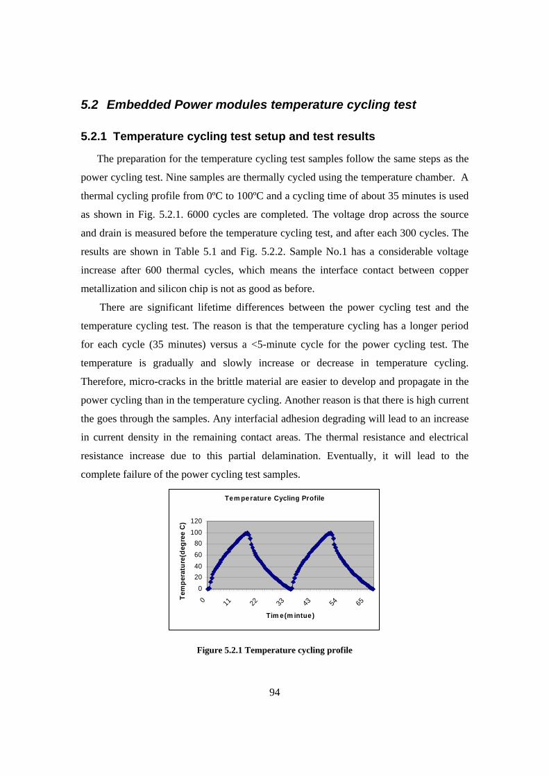
94
5.2 Embedded Power modules temperature cycling test
5.2.1 Temperature cycling test setup and test results
The preparation for the temperature cycling test samples follow the same steps as the
power cycling test. Nine samples are thermally cycled using the temperature chamber. A
thermal cycling profile from 0ºC to 100ºC and a cycling time of about 35 minutes is used
as shown in Fig. 5.2.1. 6000 cycles are completed. The voltage drop across the source
and drain is measured before the temperature cycling test, and after each 300 cycles. The
results are shown in Table 5.1 and Fig. 5.2.2. Sample No.1 has a considerable voltage
increase after 600 thermal cycles, which means the interface contact between copper
metallization and silicon chip is not as good as before.
There are significant lifetime differences between the power cycling test and the
temperature cycling test. The reason is that the temperature cycling has a longer period
for each cycle (35 minutes) versus a <5-minute cycle for the power cycling test. The
temperature is gradually and slowly increase or decrease in temperature cycling.
Therefore, micro-cracks in the brittle material are easier to develop and propagate in the
power cycling than in the temperature cycling. Another reason is that there is high current
the goes through the samples. Any interfacial adhesion degrading will lead to an increase
in current density in the remaining contact areas. The thermal resistance and electrical
resistance increase due to this partial delamination. Eventually, it will lead to the
complete failure of the power cycling test samples.
Tem perature Cycling Profile
020406080
100120
0 11 22 33 43 54 65
Tim e(m intue)
Tem
pera
ture
(deg
ree
C)
Figure 5.2.1 Temperature cycling profile
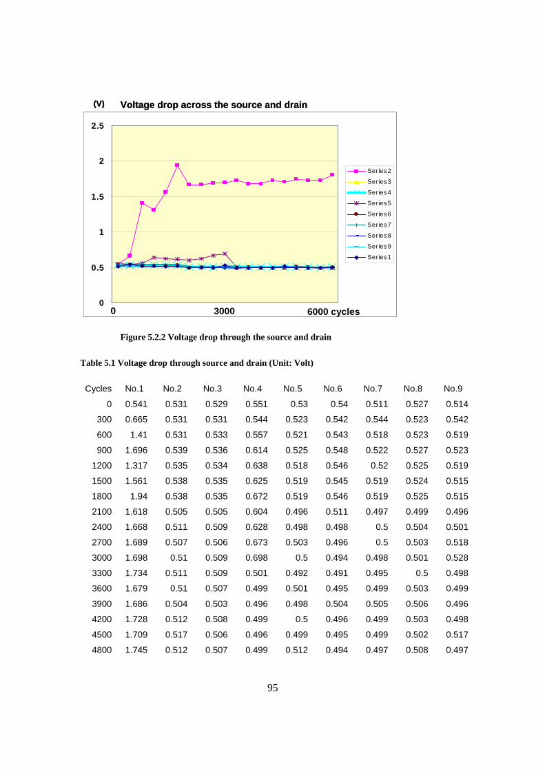
95
0
0.5
1
1.5
2
2.5
Series2
Series3
Series4
Series5
Series6
Series7
Series8
Series9
Series1
Voltage drop across the source and drain(V)
6000 cycles0 30000
0.5
1
1.5
2
2.5
Series2
Series3
Series4
Series5
Series6
Series7
Series8
Series9
Series1
Voltage drop across the source and drain(V)
6000 cycles0 3000
Figure 5.2.2 Voltage drop through the source and drain
Table 5.1 Voltage drop through source and drain (Unit: Volt)
Cycles No.1 No.2 No.3 No.4 No.5 No.6 No.7 No.8 No.9
0 0.541 0.531 0.529 0.551 0.53 0.54 0.511 0.527 0.514
300 0.665 0.531 0.531 0.544 0.523 0.542 0.544 0.523 0.542
600 1.41 0.531 0.533 0.557 0.521 0.543 0.518 0.523 0.519
900 1.696 0.539 0.536 0.614 0.525 0.548 0.522 0.527 0.523
1200 1.317 0.535 0.534 0.638 0.518 0.546 0.52 0.525 0.519
1500 1.561 0.538 0.535 0.625 0.519 0.545 0.519 0.524 0.515
1800 1.94 0.538 0.535 0.672 0.519 0.546 0.519 0.525 0.515
2100 1.618 0.505 0.505 0.604 0.496 0.511 0.497 0.499 0.496
2400 1.668 0.511 0.509 0.628 0.498 0.498 0.5 0.504 0.501
2700 1.689 0.507 0.506 0.673 0.503 0.496 0.5 0.503 0.518
3000 1.698 0.51 0.509 0.698 0.5 0.494 0.498 0.501 0.528
3300 1.734 0.511 0.509 0.501 0.492 0.491 0.495 0.5 0.498
3600 1.679 0.51 0.507 0.499 0.501 0.495 0.499 0.503 0.499
3900 1.686 0.504 0.503 0.496 0.498 0.504 0.505 0.506 0.496
4200 1.728 0.512 0.508 0.499 0.5 0.496 0.499 0.503 0.498
4500 1.709 0.517 0.506 0.496 0.499 0.495 0.499 0.502 0.517
4800 1.745 0.512 0.507 0.499 0.512 0.494 0.497 0.508 0.497
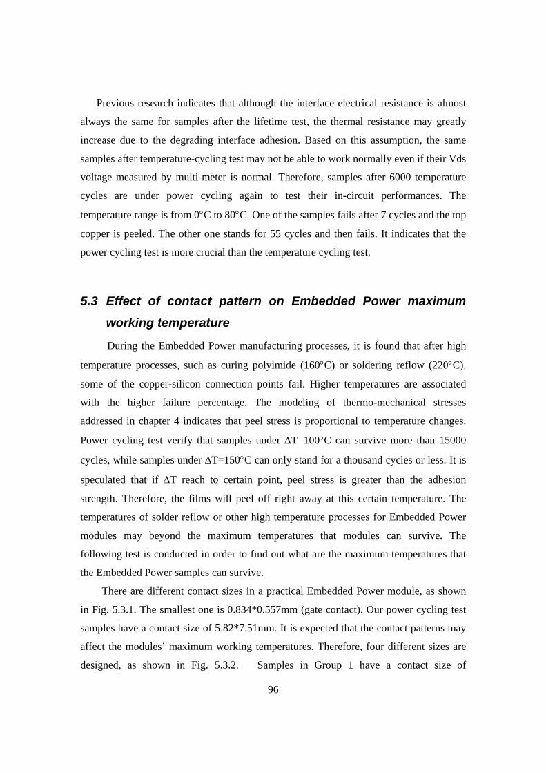
96
Previous research indicates that although the interface electrical resistance is almost
always the same for samples after the lifetime test, the thermal resistance may greatly
increase due to the degrading interface adhesion. Based on this assumption, the same
samples after temperature-cycling test may not be able to work normally even if their Vds
voltage measured by multi-meter is normal. Therefore, samples after 6000 temperature
cycles are under power cycling again to test their in-circuit performances. The
temperature range is from 0°C to 80°C. One of the samples fails after 7 cycles and the top
copper is peeled. The other one stands for 55 cycles and then fails. It indicates that the
power cycling test is more crucial than the temperature cycling test.
5.3 Effect of contact pattern on Embedded Power maximum
working temperature
During the Embedded Power manufacturing processes, it is found that after high
temperature processes, such as curing polyimide (160°C) or soldering reflow (220°C),
some of the copper-silicon connection points fail. Higher temperatures are associated
with the higher failure percentage. The modeling of thermo-mechanical stresses
addressed in chapter 4 indicates that peel stress is proportional to temperature changes.
Power cycling test verify that samples under ∆T=100°C can survive more than 15000
cycles, while samples under ∆T=150°C can only stand for a thousand cycles or less. It is
speculated that if ∆T reach to certain point, peel stress is greater than the adhesion
strength. Therefore, the films will peel off right away at this certain temperature. The
temperatures of solder reflow or other high temperature processes for Embedded Power
modules may beyond the maximum temperatures that modules can survive. The
following test is conducted in order to find out what are the maximum temperatures that
the Embedded Power samples can survive.
There are different contact sizes in a practical Embedded Power module, as shown
in Fig. 5.3.1. The smallest one is 0.834*0.557mm (gate contact). Our power cycling test
samples have a contact size of 5.82*7.51mm. It is expected that the contact patterns may
affect the modules’ maximum working temperatures. Therefore, four different sizes are
designed, as shown in Fig. 5.3.2. Samples in Group 1 have a contact size of
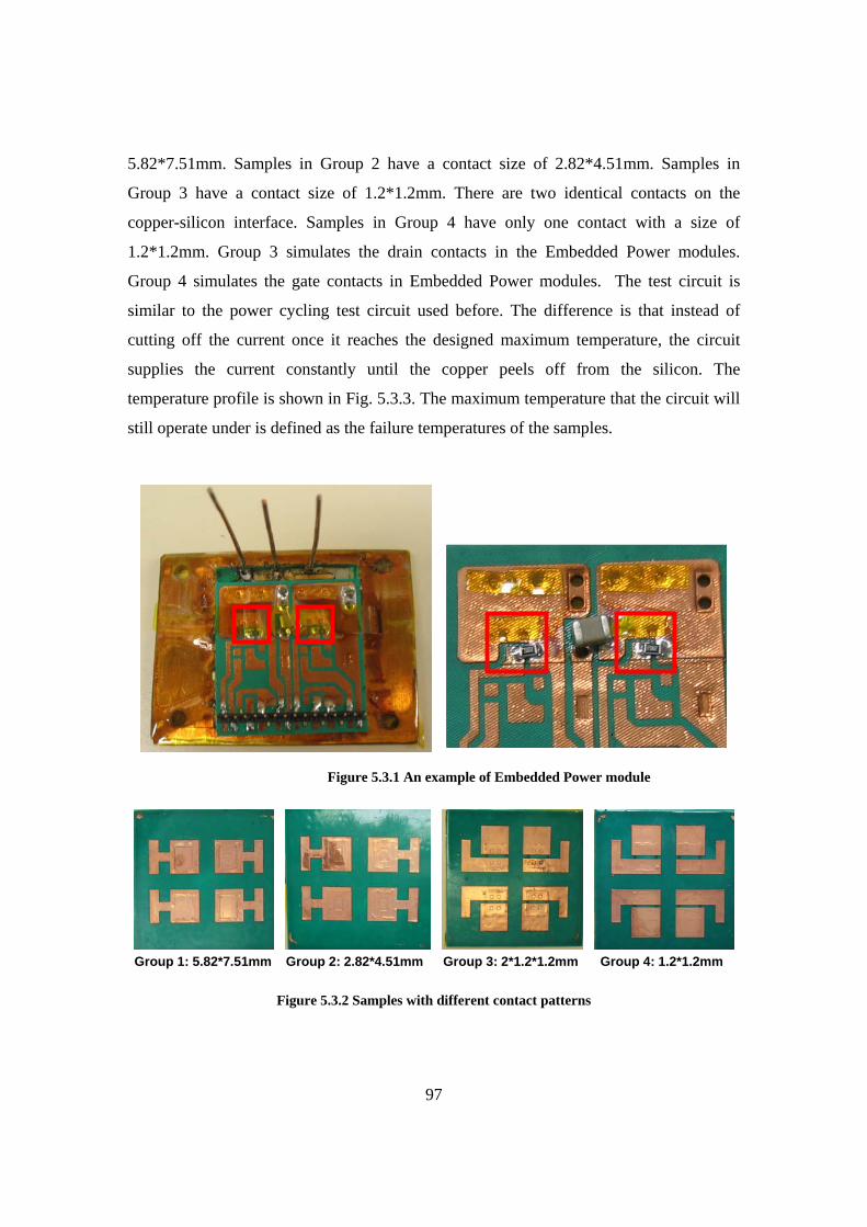
97
5.82*7.51mm. Samples in Group 2 have a contact size of 2.82*4.51mm. Samples in
Group 3 have a contact size of 1.2*1.2mm. There are two identical contacts on the
copper-silicon interface. Samples in Group 4 have only one contact with a size of
1.2*1.2mm. Group 3 simulates the drain contacts in the Embedded Power modules.
Group 4 simulates the gate contacts in Embedded Power modules. The test circuit is
similar to the power cycling test circuit used before. The difference is that instead of
cutting off the current once it reaches the designed maximum temperature, the circuit
supplies the current constantly until the copper peels off from the silicon. The
temperature profile is shown in Fig. 5.3.3. The maximum temperature that the circuit will
still operate under is defined as the failure temperatures of the samples.
Figure 5.3.1 An example of Embedded Power module
Group 4: 1.2*1.2mmGroup 3: 2*1.2*1.2mmGroup 2: 2.82*4.51mmGroup 1: 5.82*7.51mm
Figure 5.3.2 Samples with different contact patterns
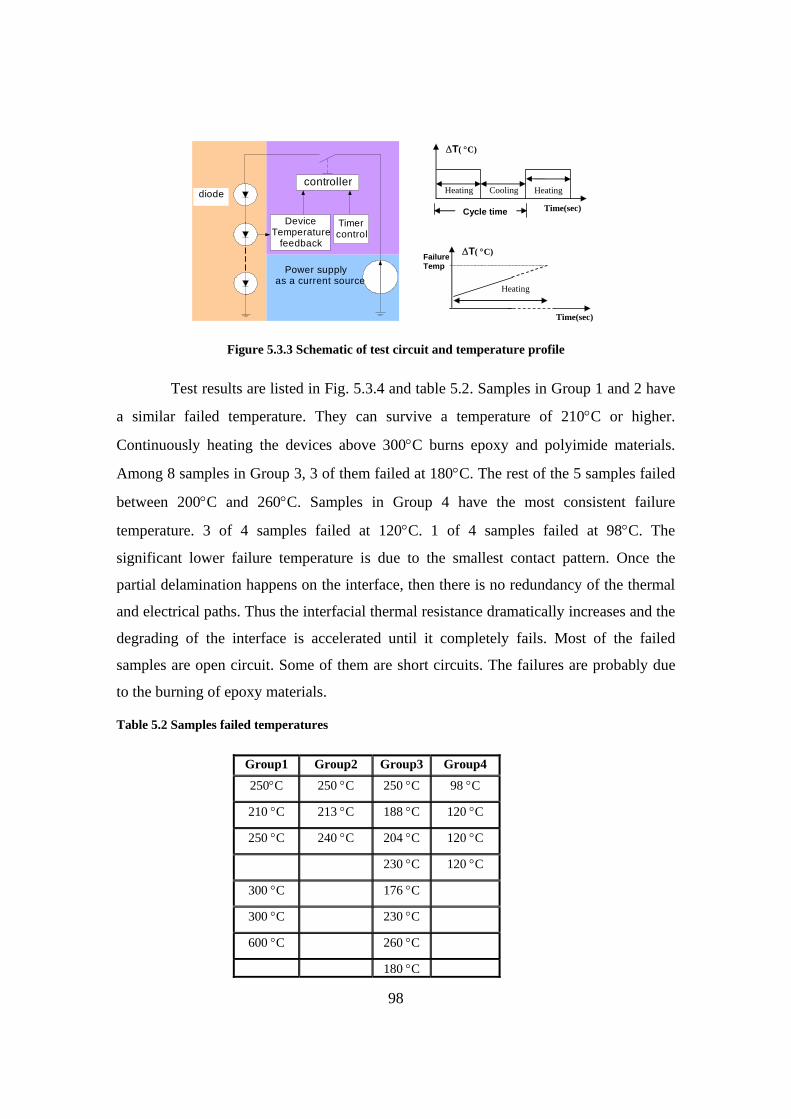
98
controller
DeviceTemperature
feedback
Timercontrol
Power supply as a current source
diode Heating Cooling Heating
∆T( °C)
Time(sec) Cycle time
Heating
∆T( °C)
Time(sec)
Failure Temp
Figure 5.3.3 Schematic of test circuit and temperature profile
Test results are listed in Fig. 5.3.4 and table 5.2. Samples in Group 1 and 2 have
a similar failed temperature. They can survive a temperature of 210°C or higher.
Continuously heating the devices above 300°C burns epoxy and polyimide materials.
Among 8 samples in Group 3, 3 of them failed at 180°C. The rest of the 5 samples failed
between 200°C and 260°C. Samples in Group 4 have the most consistent failure
temperature. 3 of 4 samples failed at 120°C. 1 of 4 samples failed at 98°C. The
significant lower failure temperature is due to the smallest contact pattern. Once the
partial delamination happens on the interface, then there is no redundancy of the thermal
and electrical paths. Thus the interfacial thermal resistance dramatically increases and the
degrading of the interface is accelerated until it completely fails. Most of the failed
samples are open circuit. Some of them are short circuits. The failures are probably due
to the burning of epoxy materials.
Table 5.2 Samples failed temperatures
Group1 Group2 Group3 Group4
250°C 250 °C 250 °C 98 °C
210 °C 213 °C 188 °C 120 °C
250 °C 240 °C 204 °C 120 °C
230 °C 120 °C
300 °C 176 °C
300 °C 230 °C
600 °C 260 °C
180 °C
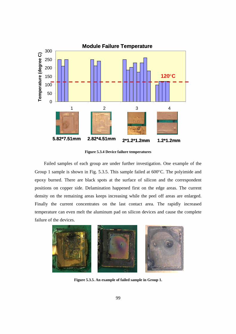
99
0
50
100
150
200
250
300
1 2 3 4
Tem
pera
ture
(deg
ree
C)
120°C
1.2*1.2mm2*1.2*1.2mm2.82*4.51mm5.82*7.51mm
Module Failure Temperature
0
50
100
150
200
250
300
1 2 3 4
Tem
pera
ture
(deg
ree
C)
120°C
1.2*1.2mm2*1.2*1.2mm2.82*4.51mm5.82*7.51mm
Module Failure Temperature
Figure 5.3.4 Device failure temperatures
Failed samples of each group are under further investigation. One example of the
Group 1 sample is shown in Fig. 5.3.5. This sample failed at 600°C. The polyimide and
epoxy burned. There are black spots at the surface of silicon and the correspondent
positions on copper side. Delamination happened first on the edge areas. The current
density on the remaining areas keeps increasing while the peel off areas are enlarged.
Finally the current concentrates on the last contact area. The rapidly increased
temperature can even melt the aluminum pad on silicon devices and cause the complete
failure of the devices.
Figure 5.3.5. An example of failed sample in Group 1.
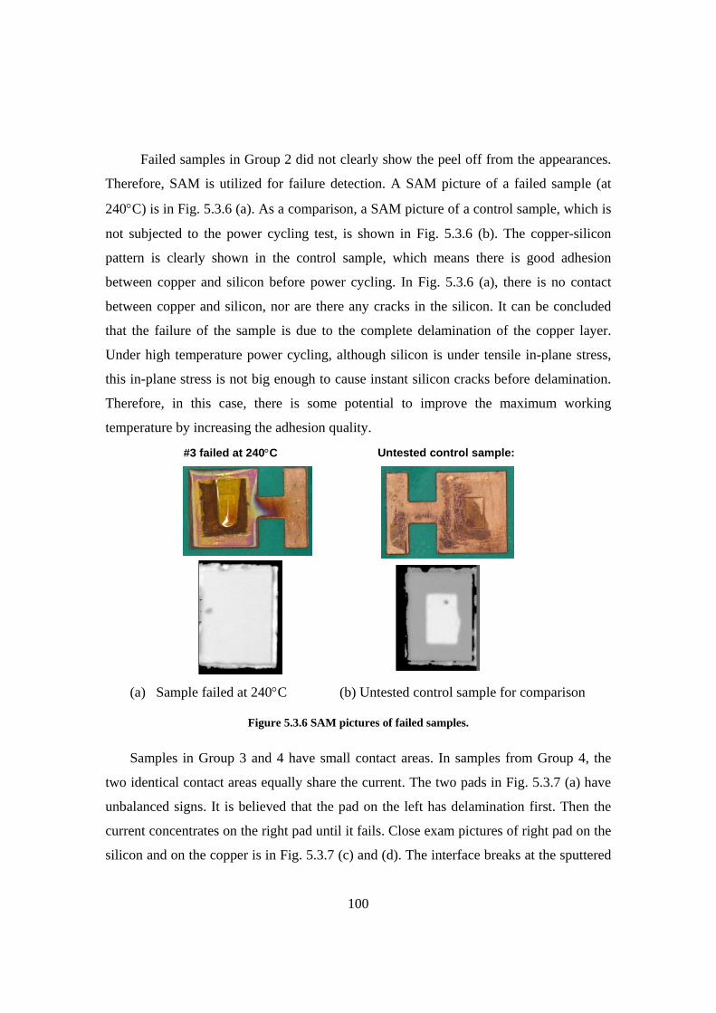
100
Failed samples in Group 2 did not clearly show the peel off from the appearances.
Therefore, SAM is utilized for failure detection. A SAM picture of a failed sample (at
240°C) is in Fig. 5.3.6 (a). As a comparison, a SAM picture of a control sample, which is
not subjected to the power cycling test, is shown in Fig. 5.3.6 (b). The copper-silicon
pattern is clearly shown in the control sample, which means there is good adhesion
between copper and silicon before power cycling. In Fig. 5.3.6 (a), there is no contact
between copper and silicon, nor are there any cracks in the silicon. It can be concluded
that the failure of the sample is due to the complete delamination of the copper layer.
Under high temperature power cycling, although silicon is under tensile in-plane stress,
this in-plane stress is not big enough to cause instant silicon cracks before delamination.
Therefore, in this case, there is some potential to improve the maximum working
temperature by increasing the adhesion quality.
#3 failed at 240°C Untested control sample:
(a) Sample failed at 240°C (b) Untested control sample for comparison
Figure 5.3.6 SAM pictures of failed samples.
Samples in Group 3 and 4 have small contact areas. In samples from Group 4, the
two identical contact areas equally share the current. The two pads in Fig. 5.3.7 (a) have
unbalanced signs. It is believed that the pad on the left has delamination first. Then the
current concentrates on the right pad until it fails. Close exam pictures of right pad on the
silicon and on the copper is in Fig. 5.3.7 (c) and (d). The interface breaks at the sputtered
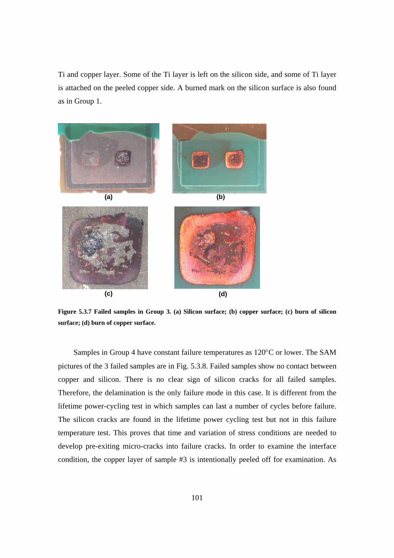
101
Ti and copper layer. Some of the Ti layer is left on the silicon side, and some of Ti layer
is attached on the peeled copper side. A burned mark on the silicon surface is also found
as in Group 1.
(a) (b)
(c) (d)
Figure 5.3.7 Failed samples in Group 3. (a) Silicon surface; (b) copper surface; (c) burn of silicon
surface; (d) burn of copper surface.
Samples in Group 4 have constant failure temperatures as 120°C or lower. The SAM
pictures of the 3 failed samples are in Fig. 5.3.8. Failed samples show no contact between
copper and silicon. There is no clear sign of silicon cracks for all failed samples.
Therefore, the delamination is the only failure mode in this case. It is different from the
lifetime power-cycling test in which samples can last a number of cycles before failure.
The silicon cracks are found in the lifetime power cycling test but not in this failure
temperature test. This proves that time and variation of stress conditions are needed to
develop pre-exiting micro-cracks into failure cracks. In order to examine the interface
condition, the copper layer of sample #3 is intentionally peeled off for examination. As
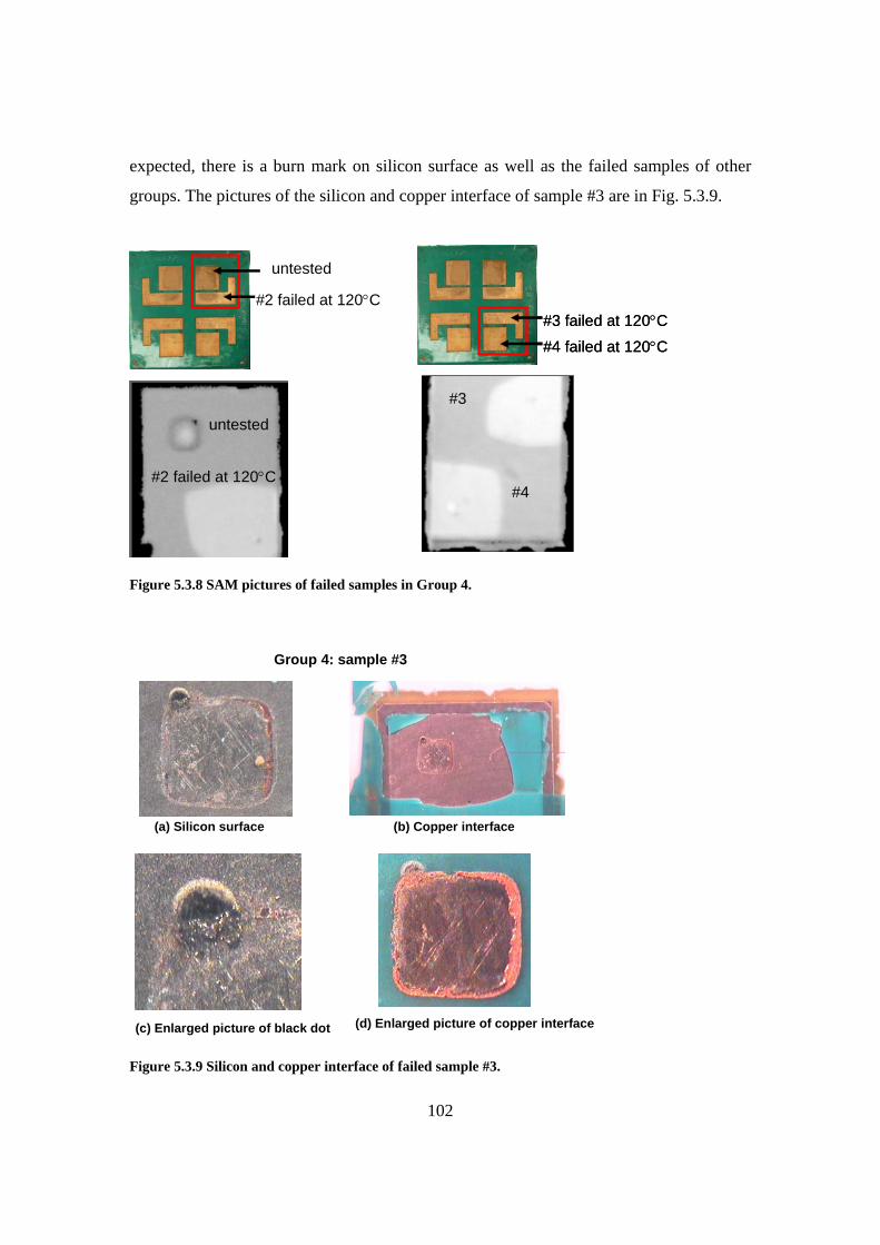
102
expected, there is a burn mark on silicon surface as well as the failed samples of other
groups. The pictures of the silicon and copper interface of sample #3 are in Fig. 5.3.9.
#2 failed at 120°C
untested
untested
#2 failed at 120°C
#3 failed at 120°C
#4 failed at 120°C
#3 failed at 120°C
#4 failed at 120°C
#3
#4
#3
#4
Figure 5.3.8 SAM pictures of failed samples in Group 4.
Group 4: sample #3
(a) Silicon surface (b) Copper interface
(c) Enlarged picture of black dot (d) Enlarged picture of copper interface
Figure 5.3.9 Silicon and copper interface of failed sample #3.
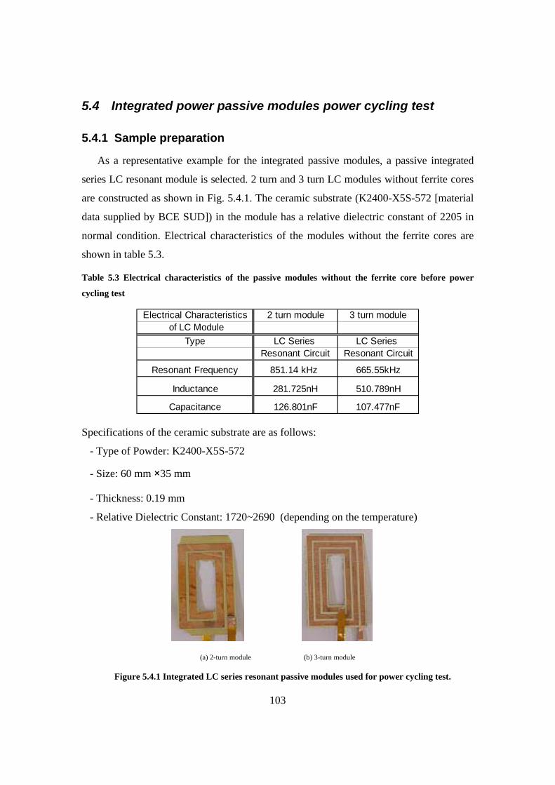
103
5.4 Integrated power passive modules power cycling test
5.4.1 Sample preparation
As a representative example for the integrated passive modules, a passive integrated
series LC resonant module is selected. 2 turn and 3 turn LC modules without ferrite cores
are constructed as shown in Fig. 5.4.1. The ceramic substrate (K2400-X5S-572 [material
data supplied by BCE SUD]) in the module has a relative dielectric constant of 2205 in
normal condition. Electrical characteristics of the modules without the ferrite cores are
shown in table 5.3.
Table 5.3 Electrical characteristics of the passive modules without the ferrite core before power
cycling test
Electrical Characteristics 2 turn module 3 turn module of LC Module
Type LC Series LC Series Resonant Circuit Resonant Circuit
Resonant Frequency 851.14 kHz 665.55kHz
Inductance 281.725nH 510.789nH
Capacitance 126.801nF 107.477nF
Specifications of the ceramic substrate are as follows:
- Type of Powder: K2400-X5S-572
- Size: 60 mm ×35 mm
- Thickness: 0.19 mm
- Relative Dielectric Constant: 1720~2690 (depending on the temperature)
(a) 2-turn module (b) 3-turn module
Figure 5.4.1 Integrated LC series resonant passive modules used for power cycling test.
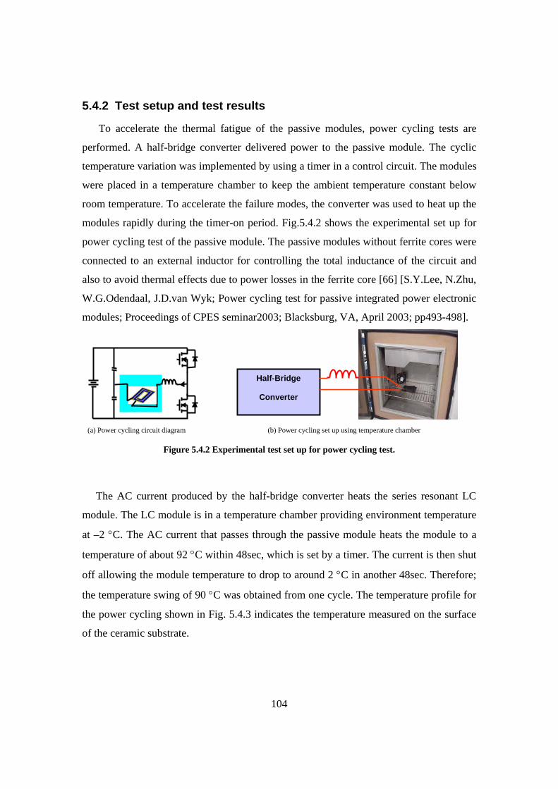
104
5.4.2 Test setup and test results
To accelerate the thermal fatigue of the passive modules, power cycling tests are
performed. A half-bridge converter delivered power to the passive module. The cyclic
temperature variation was implemented by using a timer in a control circuit. The modules
were placed in a temperature chamber to keep the ambient temperature constant below
room temperature. To accelerate the failure modes, the converter was used to heat up the
modules rapidly during the timer-on period. Fig.5.4.2 shows the experimental set up for
power cycling test of the passive module. The passive modules without ferrite cores were
connected to an external inductor for controlling the total inductance of the circuit and
also to avoid thermal effects due to power losses in the ferrite core [66] [S.Y.Lee, N.Zhu,
W.G.Odendaal, J.D.van Wyk; Power cycling test for passive integrated power electronic
modules; Proceedings of CPES seminar2003; Blacksburg, VA, April 2003; pp493-498].
(a) Power cycling circuit diagram (b) Power cycling set up using temperature chamber
Figure 5.4.2 Experimental test set up for power cycling test.
The AC current produced by the half-bridge converter heats the series resonant LC
module. The LC module is in a temperature chamber providing environment temperature
at –2 °C. The AC current that passes through the passive module heats the module to a
temperature of about 92 °C within 48sec, which is set by a timer. The current is then shut
off allowing the module temperature to drop to around 2 °C in another 48sec. Therefore;
the temperature swing of 90 °C was obtained from one cycle. The temperature profile for
the power cycling shown in Fig. 5.4.3 indicates the temperature measured on the surface
of the ceramic substrate.
Half-Bridge
Converter
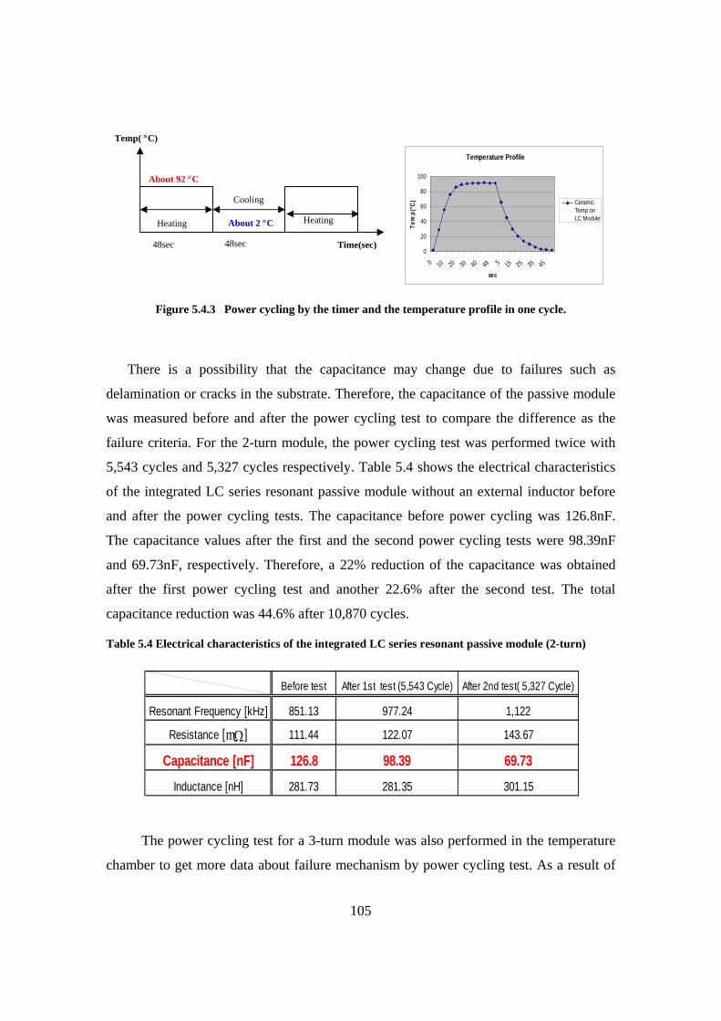
105
Temperature Profile
0
20
40
60
80
100
0 10 20 30 40 48 5 15 25 35 45
sec
Tem
p(°C
) CeramicTemp onLC Module
Figure 5.4.3 Power cycling by the timer and the temperature profile in one cycle.
There is a possibility that the capacitance may change due to failures such as
delamination or cracks in the substrate. Therefore, the capacitance of the passive module
was measured before and after the power cycling test to compare the difference as the
failure criteria. For the 2-turn module, the power cycling test was performed twice with
5,543 cycles and 5,327 cycles respectively. Table 5.4 shows the electrical characteristics
of the integrated LC series resonant passive module without an external inductor before
and after the power cycling tests. The capacitance before power cycling was 126.8nF.
The capacitance values after the first and the second power cycling tests were 98.39nF
and 69.73nF, respectively. Therefore, a 22% reduction of the capacitance was obtained
after the first power cycling test and another 22.6% after the second test. The total
capacitance reduction was 44.6% after 10,870 cycles.
Table 5.4 Electrical characteristics of the integrated LC series resonant passive module (2-turn)
Before test After 1st test (5,543 Cycle) After 2nd test( 5,327 Cycle)
Resonant Frequency [kHz] 851.13 977.24 1,122
Resistance [mΩ] 111.44 122.07 143.67
Capacitance [nF] 126.8 98.39 69.73Inductance [nH] 281.73 281.35 301.15
The power cycling test for a 3-turn module was also performed in the temperature
chamber to get more data about failure mechanism by power cycling test. As a result of
48sec Time(sec)48sec
Cooling
About 92 °C
About 2 °C Heating
Temp( °C)
Heating
106
this work, impedance characteristics for the 3-turn module were measured before and
after 4,601 cycling (the first test), 2,479 cycling (the second test) and 713 cycling (the
third test), respectively. For the first 4,601 cycling, the temperature inside the chamber
was –2 °C and the temperature swing of the passive module was between 86 ~ 87 °C
(from about 2.5°C to about 89°C). The electrical characteristics before and after the
power cycling test are shown in table 5.5. The measured capacitance before power
cycling was 107.48nF and the capacitance after the first power cycling test was 106.95nF.
It can be noted that there is no significant change of the capacitance from the first power
cycling test. To accelerate the failure of the passive module, the temperature inside of the
chamber is adjusted to a lower temperature of -10 °C and the temperature variation of the
passive module is also adjusted to about 97 °C (from about –6 °C to about 91°C). The
electrical characteristics after 2,479 cycling and 713 cycling performed by these power
cycling conditions are also shown in table IV, respectively. From these power cycling
tests, we can see that the capacitances of the passive module were reduced from 106.95nF
to 95.28nF (for the second test) and from 95.28nF to 68.1nF (for the third test). Therefore,
a 36.6% reduction of the capacitance for the 3-turn module was obtained after a total of
7,793 cycles.
Table 5.5 Electrical characteristics of the integrated LC series resonant passive module (3-turn)
Before test After 1st test After 2nd test After 3rd test(4,601 Cycle) ( 2,479 Cycle) ( 713 Cycle)
Resonant Frequency [kHz] 665.55 665.55 705.32 839.47
Resistance [mΩ] 144.96 149.96 159.4 177.9
Capacitance [nF] 107.48 106.95 95.28 68.1Inductance [nH] 510.79 525.44 534.81 527.61
5.4.3 Failure mode analysis for integrated passive modules
This capacitance reduction is investigated by optical microscopic images over the
cross section of the passive module. The sample module fabricated for power cycling is
first encapsulated with a crystal bond and then cut into several parts using a diamond saw.
After cutting the module, the crystal bond is removed from each part by using acetone.
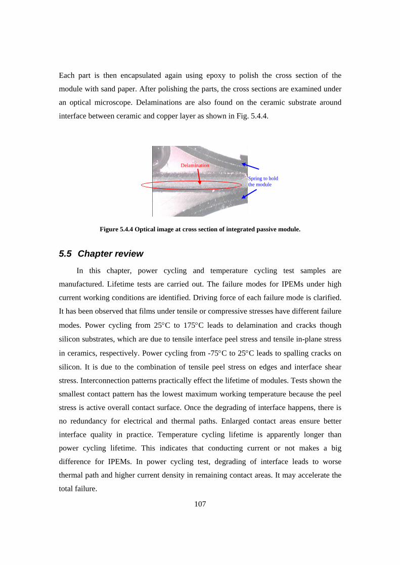
107
Each part is then encapsulated again using epoxy to polish the cross section of the
module with sand paper. After polishing the parts, the cross sections are examined under
an optical microscope. Delaminations are also found on the ceramic substrate around
interface between ceramic and copper layer as shown in Fig. 5.4.4.
Figure 5.4.4 Optical image at cross section of integrated passive module.
5.5 Chapter review
In this chapter, power cycling and temperature cycling test samples are
manufactured. Lifetime tests are carried out. The failure modes for IPEMs under high
current working conditions are identified. Driving force of each failure mode is clarified.
It has been observed that films under tensile or compressive stresses have different failure
modes. Power cycling from 25°C to 175°C leads to delamination and cracks though
silicon substrates, which are due to tensile interface peel stress and tensile in-plane stress
in ceramics, respectively. Power cycling from -75°C to 25°C leads to spalling cracks on
silicon. It is due to the combination of tensile peel stress on edges and interface shear
stress. Interconnection patterns practically effect the lifetime of modules. Tests shown the
smallest contact pattern has the lowest maximum working temperature because the peel
stress is active overall contact surface. Once the degrading of interface happens, there is
no redundancy for electrical and thermal paths. Enlarged contact areas ensure better
interface quality in practice. Temperature cycling lifetime is apparently longer than
power cycling lifetime. This indicates that conducting current or not makes a big
difference for IPEMs. In power cycling test, degrading of interface leads to worse
thermal path and higher current density in remaining contact areas. It may accelerate the
total failure.
Delamination
Spring to hold the module

108
By correlating analytical modeling with experimental results, we have more
confidence to utilize analytical modeling to optimize IPEMs’ geometry and material
parameters for better lifetime performances.
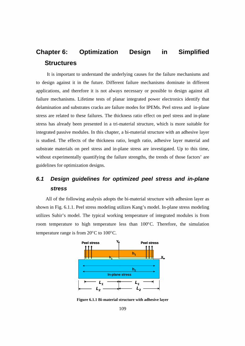
109
Chapter 6: Optimization Design in Simplified Structures
It is important to understand the underlying causes for the failure mechanisms and
to design against it in the future. Different failure mechanisms dominate in different
applications, and therefore it is not always necessary or possible to design against all
failure mechanisms. Lifetime tests of planar integrated power electronics identify that
delamination and substrates cracks are failure modes for IPEMs. Peel stress and in-plane
stress are related to these failures. The thickness ratio effect on peel stress and in-plane
stress has already been presented in a tri-material structure, which is more suitable for
integrated passive modules. In this chapter, a bi-material structure with an adhesive layer
is studied. The effects of the thickness ratio, length ratio, adhesive layer material and
substrate materials on peel stress and in-plane stress are investigated. Up to this time,
without experimentally quantifying the failure strengths, the trends of those factors’ are
guidelines for optimization designs.
6.1 Design guidelines for optimized peel stress and in-plane
stress
All of the following analysis adopts the bi-material structure with adhesion layer as
shown in Fig. 6.1.1. Peel stress modeling utilizes Kang’s model. In-plane stress modeling
utilizes Suhir’s model. The typical working temperature of integrated modules is from
room temperature to high temperature less than 100°C. Therefore, the simulation
temperature range is from 20°C to 100°C.
h2
h1ha X
Y Peel stressPeel stress
In-plane stress
L1 L1L2 L2
h2
h1ha X
Y Peel stressPeel stress
In-plane stress
L1 L1L2 L2
Figure 6.1.1 Bi-material structure with adhesive layer
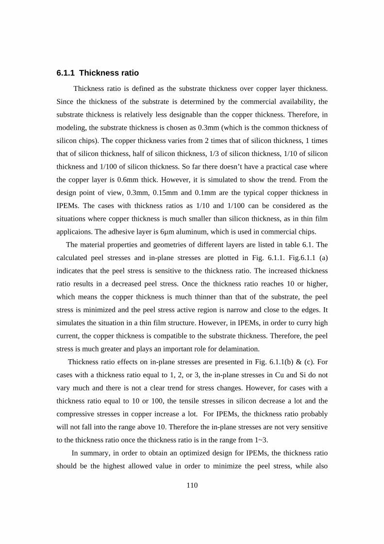
110
6.1.1 Thickness ratio
Thickness ratio is defined as the substrate thickness over copper layer thickness.
Since the thickness of the substrate is determined by the commercial availability, the
substrate thickness is relatively less designable than the copper thickness. Therefore, in
modeling, the substrate thickness is chosen as 0.3mm (which is the common thickness of
silicon chips). The copper thickness varies from 2 times that of silicon thickness, 1 times
that of silicon thickness, half of silicon thickness, 1/3 of silicon thickness, 1/10 of silicon
thickness and 1/100 of silicon thickness. So far there doesn’t have a practical case where
the copper layer is 0.6mm thick. However, it is simulated to show the trend. From the
design point of view, 0.3mm, 0.15mm and 0.1mm are the typical copper thickness in
IPEMs. The cases with thickness ratios as 1/10 and 1/100 can be considered as the
situations where copper thickness is much smaller than silicon thickness, as in thin film
applicaions. The adhesive layer is 6µm aluminum, which is used in commercial chips.
The material properties and geometries of different layers are listed in table 6.1. The
calculated peel stresses and in-plane stresses are plotted in Fig. 6.1.1. Fig.6.1.1 (a)
indicates that the peel stress is sensitive to the thickness ratio. The increased thickness
ratio results in a decreased peel stress. Once the thickness ratio reaches 10 or higher,
which means the copper thickness is much thinner than that of the substrate, the peel
stress is minimized and the peel stress active region is narrow and close to the edges. It
simulates the situation in a thin film structure. However, in IPEMs, in order to curry high
current, the copper thickness is compatible to the substrate thickness. Therefore, the peel
stress is much greater and plays an important role for delamination.
Thickness ratio effects on in-plane stresses are presented in Fig. 6.1.1(b) & (c). For
cases with a thickness ratio equal to 1, 2, or 3, the in-plane stresses in Cu and Si do not
vary much and there is not a clear trend for stress changes. However, for cases with a
thickness ratio equal to 10 or 100, the tensile stresses in silicon decrease a lot and the
compressive stresses in copper increase a lot. For IPEMs, the thickness ratio probably
will not fall into the range above 10. Therefore the in-plane stresses are not very sensitive
to the thickness ratio once the thickness ratio is in the range from 1~3.
In summary, in order to obtain an optimized design for IPEMs, the thickness ratio
should be the highest allowed value in order to minimize the peel stress, while also
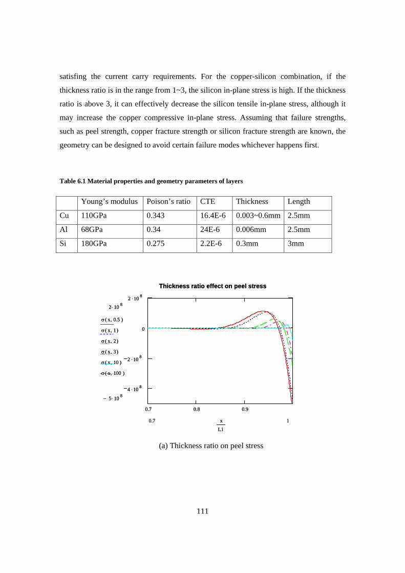
111
satisfing the current carry requirements. For the copper-silicon combination, if the
thickness ratio is in the range from 1~3, the silicon in-plane stress is high. If the thickness
ratio is above 3, it can effectively decrease the silicon tensile in-plane stress, although it
may increase the copper compressive in-plane stress. Assuming that failure strengths,
such as peel strength, copper fracture strength or silicon fracture strength are known, the
geometry can be designed to avoid certain failure modes whichever happens first.
Table 6.1 Material properties and geometry parameters of layers
Young’s modulus Poison’s ratio CTE Thickness Length
Cu 110GPa 0.343 16.4E-6 0.003~0.6mm 2.5mm
Al 68GPa 0.34 24E-6 0.006mm 2.5mm
Si 180GPa 0.275 2.2E-6 0.3mm 3mm
0.7 0.8 0.9
4 .10 8
2 .10 8
0
2 .10 8
2 10 8⋅
5− 10 8⋅
σ x 0.5,( )
σ x 1,( )
σ x 2,( )
σ x 3,( )
σ x 10,( )
σ x 100,( )
10.7 x
L1
Thickness ratio effect on peel stress
0.7 0.8 0.9
4 .10 8
2 .10 8
0
2 .10 8
2 10 8⋅
5− 10 8⋅
σ x 0.5,( )
σ x 1,( )
σ x 2,( )
σ x 3,( )
σ x 10,( )
σ x 100,( )
10.7 x
L1
Thickness ratio effect on peel stress
(a) Thickness ratio on peel stress
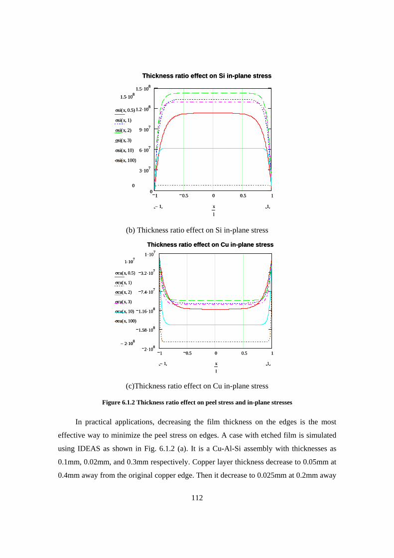
112
Thickness ratio effect on Si in-plane stress
1 0.5 0 0.5 10
3 .107
6 .107
9 .107
1.2 .108
1.5 .108
1.5 108⋅
0
σsi x 0.5,( )
σsi x 1,( )
σsi x 2,( )
σsi x 3,( )
σsi x 10,( )
σsi x 100,( )
11− x
l
Thickness ratio effect on Si in-plane stress
1 0.5 0 0.5 10
3 .107
6 .107
9 .107
1.2 .108
1.5 .108
1.5 108⋅
0
σsi x 0.5,( )
σsi x 1,( )
σsi x 2,( )
σsi x 3,( )
σsi x 10,( )
σsi x 100,( )
11− x
l (b) Thickness ratio effect on Si in-plane stress
Thickness ratio effect on Cu in-plane stress
1 0.5 0 0.5 12 .108
1.58 .108
1.16 .108
7.4 .107
3.2 .107
1 .107
1 107⋅
2− 108⋅
σcu x 0.5,( )
σcu x 1,( )
σcu x 2,( )
σcu x 3,( )
σcu x 10,( )
σcu x 100,( )
11− x
l
Thickness ratio effect on Cu in-plane stress
1 0.5 0 0.5 12 .108
1.58 .108
1.16 .108
7.4 .107
3.2 .107
1 .107
1 107⋅
2− 108⋅
σcu x 0.5,( )
σcu x 1,( )
σcu x 2,( )
σcu x 3,( )
σcu x 10,( )
σcu x 100,( )
11− x
l
(c)Thickness ratio effect on Cu in-plane stress
Figure 6.1.2 Thickness ratio effect on peel stress and in-plane stresses
In practical applications, decreasing the film thickness on the edges is the most
effective way to minimize the peel stress on edges. A case with etched film is simulated
using IDEAS as shown in Fig. 6.1.2 (a). It is a Cu-Al-Si assembly with thicknesses as
0.1mm, 0.02mm, and 0.3mm respectively. Copper layer thickness decrease to 0.05mm at
0.4mm away from the original copper edge. Then it decrease to 0.025mm at 0.2mm away
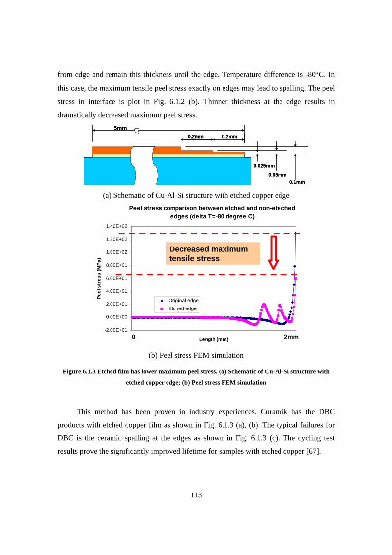
113
from edge and remain this thickness until the edge. Temperature difference is -80°C. In
this case, the maximum tensile peel stress exactly on edges may lead to spalling. The peel
stress in interface is plot in Fig. 6.1.2 (b). Thinner thickness at the edge results in
dramatically decreased maximum peel stress.
0.025mm
0.05mm0.1mm
0.2mm 0.2mm5mm
0.025mm
0.05mm0.1mm
0.2mm0.2mm 0.2mm5mm
(a) Schematic of Cu-Al-Si structure with etched copper edge
Peel stress comparison between etched and non-eteched edges (delta T=-80 degree C)
-2.00E+01
0.00E+00
2.00E+01
4.00E+01
6.00E+01
8.00E+01
1.00E+02
1.20E+02
1.40E+02
Length (mm)
Peel
str
ess
(MPa
)
Original edge
Etched edge
0 2mm
Peel stress comparison between etched and non-eteched edges (delta T=-80 degree C)
-2.00E+01
0.00E+00
2.00E+01
4.00E+01
6.00E+01
8.00E+01
1.00E+02
1.20E+02
1.40E+02
Length (mm)
Peel
str
ess
(MPa
)
Original edge
Etched edge
0 2mm
Decreased maximum tensile stress
Peel stress comparison between etched and non-eteched edges (delta T=-80 degree C)
-2.00E+01
0.00E+00
2.00E+01
4.00E+01
6.00E+01
8.00E+01
1.00E+02
1.20E+02
1.40E+02
Length (mm)
Peel
str
ess
(MPa
)
Original edge
Etched edge
0 2mm
Peel stress comparison between etched and non-eteched edges (delta T=-80 degree C)
-2.00E+01
0.00E+00
2.00E+01
4.00E+01
6.00E+01
8.00E+01
1.00E+02
1.20E+02
1.40E+02
Length (mm)
Peel
str
ess
(MPa
)
Original edge
Etched edge
0 2mm
Decreased maximum tensile stress
(b) Peel stress FEM simulation
Figure 6.1.3 Etched film has lower maximum peel stress. (a) Schematic of Cu-Al-Si structure with
etched copper edge; (b) Peel stress FEM simulation
This method has been proven in industry experiences. Curamik has the DBC
products with etched copper film as shown in Fig. 6.1.3 (a), (b). The typical failures for
DBC is the ceramic spalling at the edges as shown in Fig. 6.1.3 (c). The cycling test
results prove the significantly improved lifetime for samples with etched copper [67].
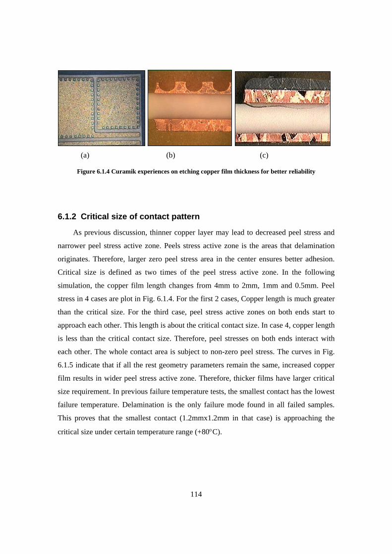
114
(a) (b) (c)
Figure 6.1.4 Curamik experiences on etching copper film thickness for better reliability
6.1.2 Critical size of contact pattern
As previous discussion, thinner copper layer may lead to decreased peel stress and
narrower peel stress active zone. Peels stress active zone is the areas that delamination
originates. Therefore, larger zero peel stress area in the center ensures better adhesion.
Critical size is defined as two times of the peel stress active zone. In the following
simulation, the copper film length changes from 4mm to 2mm, 1mm and 0.5mm. Peel
stress in 4 cases are plot in Fig. 6.1.4. For the first 2 cases, Copper length is much greater
than the critical size. For the third case, peel stress active zones on both ends start to
approach each other. This length is about the critical contact size. In case 4, copper length
is less than the critical contact size. Therefore, peel stresses on both ends interact with
each other. The whole contact area is subject to non-zero peel stress. The curves in Fig.
6.1.5 indicate that if all the rest geometry parameters remain the same, increased copper
film results in wider peel stress active zone. Therefore, thicker films have larger critical
size requirement. In previous failure temperature tests, the smallest contact has the lowest
failure temperature. Delamination is the only failure mode found in all failed samples.
This proves that the smallest contact (1.2mmx1.2mm in that case) is approaching the
critical size under certain temperature range (+80°C).
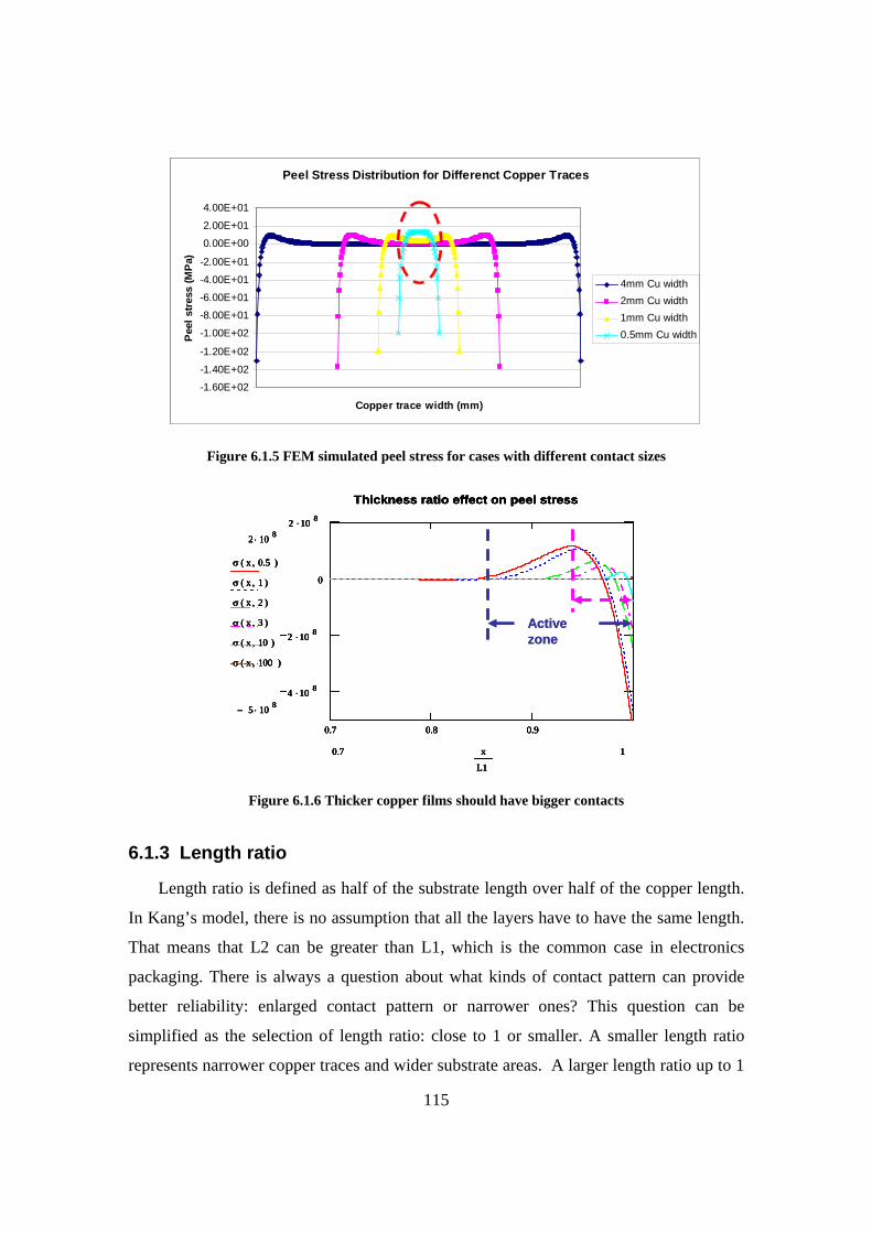
115
Peel Stress Distribution for Differenct Copper Traces
-1.60E+02
-1.40E+02
-1.20E+02
-1.00E+02
-8.00E+01
-6.00E+01
-4.00E+01
-2.00E+01
0.00E+00
2.00E+01
4.00E+01
Copper trace width (mm)
Pee
l str
ess
(MP
a)
4mm Cu width2mm Cu width1mm Cu width0.5mm Cu width
Peel Stress Distribution for Differenct Copper Traces
-1.60E+02
-1.40E+02
-1.20E+02
-1.00E+02
-8.00E+01
-6.00E+01
-4.00E+01
-2.00E+01
0.00E+00
2.00E+01
4.00E+01
Copper trace width (mm)
Pee
l str
ess
(MP
a)
4mm Cu width2mm Cu width1mm Cu width0.5mm Cu width
Figure 6.1.5 FEM simulated peel stress for cases with different contact sizes
0.7 0.8 0.9
4 .10 8
2 .10 8
0
2 .10 8
2 10 8⋅
5− 10 8⋅
σ x 0.5,( )
σ x 1,( )
σ x 2,( )
σ x 3,( )
σ x 10,( )
σ x 100,( )
10.7 x
L1
Thickness ratio effect on peel stress
0.7 0.8 0.9
4 .10 8
2 .10 8
0
2 .10 8
2 10 8⋅
5− 10 8⋅
σ x 0.5,( )
σ x 1,( )
σ x 2,( )
σ x 3,( )
σ x 10,( )
σ x 100,( )
10.7 x
L1
Thickness ratio effect on peel stress
Active zone
0.7 0.8 0.9
4 .10 8
2 .10 8
0
2 .10 8
2 10 8⋅
5− 10 8⋅
σ x 0.5,( )
σ x 1,( )
σ x 2,( )
σ x 3,( )
σ x 10,( )
σ x 100,( )
10.7 x
L1
Thickness ratio effect on peel stress
0.7 0.8 0.9
4 .10 8
2 .10 8
0
2 .10 8
2 10 8⋅
5− 10 8⋅
σ x 0.5,( )
σ x 1,( )
σ x 2,( )
σ x 3,( )
σ x 10,( )
σ x 100,( )
10.7 x
L1
Thickness ratio effect on peel stress
Active zone
Figure 6.1.6 Thicker copper films should have bigger contacts
6.1.3 Length ratio
Length ratio is defined as half of the substrate length over half of the copper length.
In Kang’s model, there is no assumption that all the layers have to have the same length.
That means that L2 can be greater than L1, which is the common case in electronics
packaging. There is always a question about what kinds of contact pattern can provide
better reliability: enlarged contact pattern or narrower ones? This question can be
simplified as the selection of length ratio: close to 1 or smaller. A smaller length ratio
represents narrower copper traces and wider substrate areas. A larger length ratio up to 1
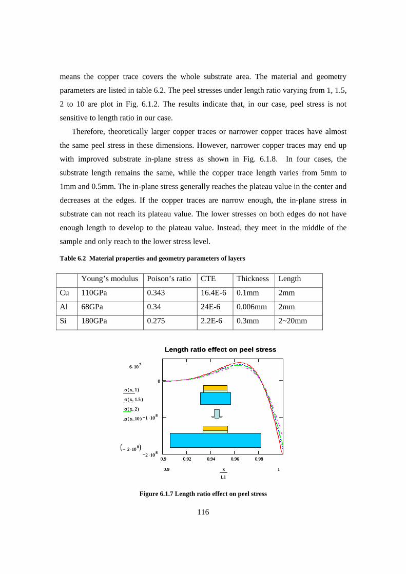
116
means the copper trace covers the whole substrate area. The material and geometry
parameters are listed in table 6.2. The peel stresses under length ratio varying from 1, 1.5,
2 to 10 are plot in Fig. 6.1.2. The results indicate that, in our case, peel stress is not
sensitive to length ratio in our case.
Therefore, theoretically larger copper traces or narrower copper traces have almost
the same peel stress in these dimensions. However, narrower copper traces may end up
with improved substrate in-plane stress as shown in Fig. 6.1.8. In four cases, the
substrate length remains the same, while the copper trace length varies from 5mm to
1mm and 0.5mm. The in-plane stress generally reaches the plateau value in the center and
decreases at the edges. If the copper traces are narrow enough, the in-plane stress in
substrate can not reach its plateau value. The lower stresses on both edges do not have
enough length to develop to the plateau value. Instead, they meet in the middle of the
sample and only reach to the lower stress level.
Table 6.2 Material properties and geometry parameters of layers
Young’s modulus Poison’s ratio CTE Thickness Length
Cu 110GPa 0.343 16.4E-6 0.1mm 2mm
Al 68GPa 0.34 24E-6 0.006mm 2mm
Si 180GPa 0.275 2.2E-6 0.3mm 2~20mm
0.9 0.92 0.94 0.96 0.982 .10 8
1 .10 8
0
6 10 7⋅
2− 10 8⋅( )
σ x 1,( )
σ x 1.5,( )
σ x 2,( )
σ x 10,( )
10.9 x
L1
Length ratio effect on peel stress
0.9 0.92 0.94 0.96 0.982 .10 8
1 .10 8
0
6 10 7⋅
2− 10 8⋅( )
σ x 1,( )
σ x 1.5,( )
σ x 2,( )
σ x 10,( )
10.9 x
L1
Length ratio effect on peel stress
Figure 6.1.7 Length ratio effect on peel stress
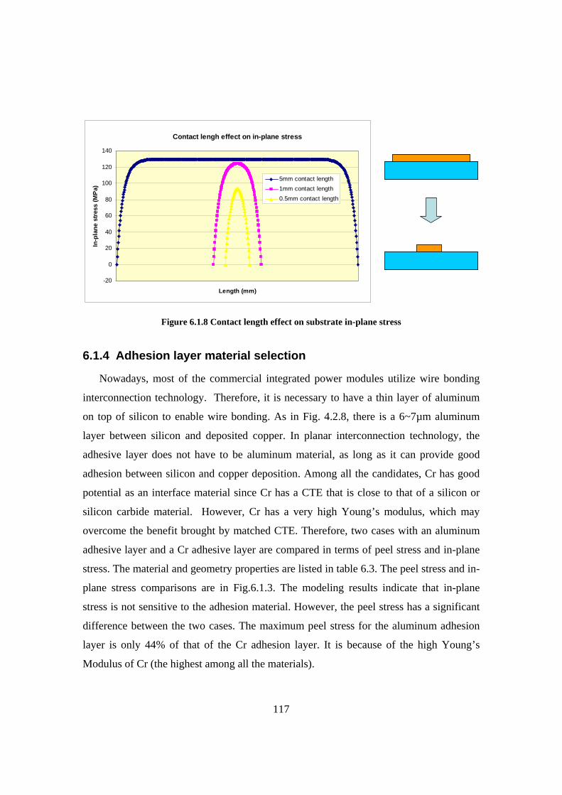
117
Contact lengh effect on in-plane stress
-20
0
20
40
60
80
100
120
140
Length (mm)
In-p
lane
stre
ss (M
Pa)
5mm contact length1mm contact length0.5mm contact length
Figure 6.1.8 Contact length effect on substrate in-plane stress
6.1.4 Adhesion layer material selection
Nowadays, most of the commercial integrated power modules utilize wire bonding
interconnection technology. Therefore, it is necessary to have a thin layer of aluminum
on top of silicon to enable wire bonding. As in Fig. 4.2.8, there is a 6~7µm aluminum
layer between silicon and deposited copper. In planar interconnection technology, the
adhesive layer does not have to be aluminum material, as long as it can provide good
adhesion between silicon and copper deposition. Among all the candidates, Cr has good
potential as an interface material since Cr has a CTE that is close to that of a silicon or
silicon carbide material. However, Cr has a very high Young’s modulus, which may
overcome the benefit brought by matched CTE. Therefore, two cases with an aluminum
adhesive layer and a Cr adhesive layer are compared in terms of peel stress and in-plane
stress. The material and geometry properties are listed in table 6.3. The peel stress and in-
plane stress comparisons are in Fig.6.1.3. The modeling results indicate that in-plane
stress is not sensitive to the adhesion material. However, the peel stress has a significant
difference between the two cases. The maximum peel stress for the aluminum adhesion
layer is only 44% of that of the Cr adhesion layer. It is because of the high Young’s
Modulus of Cr (the highest among all the materials).
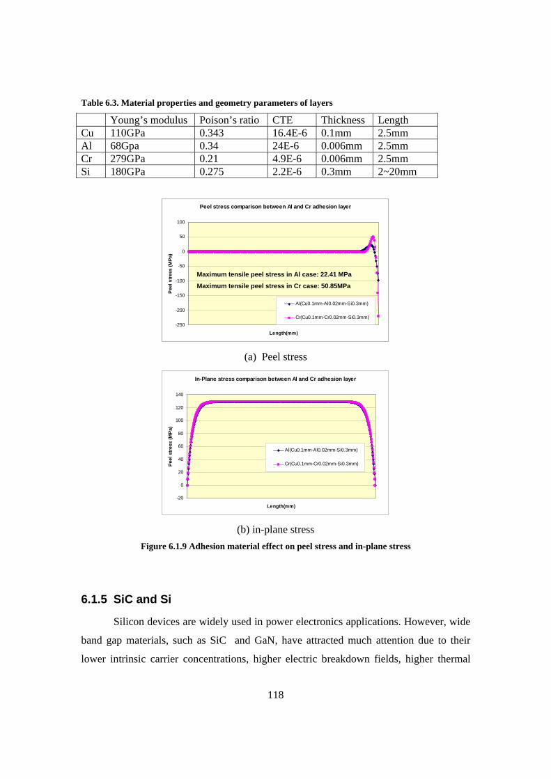
118
Table 6.3. Material properties and geometry parameters of layers
Young’s modulus Poison’s ratio CTE Thickness Length Cu 110GPa 0.343 16.4E-6 0.1mm 2.5mm Al 68Gpa 0.34 24E-6 0.006mm 2.5mm Cr 279GPa 0.21 4.9E-6 0.006mm 2.5mm Si 180GPa 0.275 2.2E-6 0.3mm 2~20mm
Peel stress comparison between Al and Cr adhesion layer
-250
-200
-150
-100
-50
0
50
100
Length(mm)
Peel
stre
ss (M
Pa)
Al(Cu0.1mm-Al0.02mm-Si0.3mm)
Cr(Cu0.1mm-Cr0.02mm-Si0.3mm)
Maximum tensile peel stress in Al case: 22.41 MPa
Maximum tensile peel stress in Cr case: 50.85MPa
Peel stress comparison between Al and Cr adhesion layer
-250
-200
-150
-100
-50
0
50
100
Length(mm)
Peel
stre
ss (M
Pa)
Al(Cu0.1mm-Al0.02mm-Si0.3mm)
Cr(Cu0.1mm-Cr0.02mm-Si0.3mm)
Maximum tensile peel stress in Al case: 22.41 MPa
Maximum tensile peel stress in Cr case: 50.85MPa
(a) Peel stress
In-Plane stress comparison between Al and Cr adhesion layer
-20
0
20
40
60
80
100
120
140
Length(mm)
Peel
stre
ss (M
Pa)
Al(Cu0.1mm-Al0.02mm-Si0.3mm)
Cr(Cu0.1mm-Cr0.02mm-Si0.3mm)
(b) in-plane stress
Figure 6.1.9 Adhesion material effect on peel stress and in-plane stress
6.1.5 SiC and Si
Silicon devices are widely used in power electronics applications. However, wide
band gap materials, such as SiC and GaN, have attracted much attention due to their
lower intrinsic carrier concentrations, higher electric breakdown fields, higher thermal
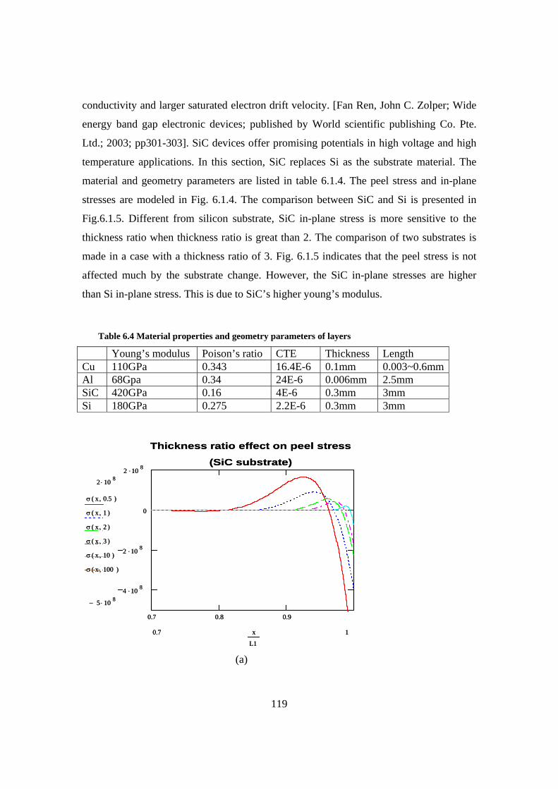
119
conductivity and larger saturated electron drift velocity. [Fan Ren, John C. Zolper; Wide
energy band gap electronic devices; published by World scientific publishing Co. Pte.
Ltd.; 2003; pp301-303]. SiC devices offer promising potentials in high voltage and high
temperature applications. In this section, SiC replaces Si as the substrate material. The
material and geometry parameters are listed in table 6.1.4. The peel stress and in-plane
stresses are modeled in Fig. 6.1.4. The comparison between SiC and Si is presented in
Fig.6.1.5. Different from silicon substrate, SiC in-plane stress is more sensitive to the
thickness ratio when thickness ratio is great than 2. The comparison of two substrates is
made in a case with a thickness ratio of 3. Fig. 6.1.5 indicates that the peel stress is not
affected much by the substrate change. However, the SiC in-plane stresses are higher
than Si in-plane stress. This is due to SiC’s higher young’s modulus.
Table 6.4 Material properties and geometry parameters of layers
Young’s modulus Poison’s ratio CTE Thickness Length Cu 110GPa 0.343 16.4E-6 0.1mm 0.003~0.6mm Al 68Gpa 0.34 24E-6 0.006mm 2.5mm SiC 420GPa 0.16 4E-6 0.3mm 3mm Si 180GPa 0.275 2.2E-6 0.3mm 3mm
0.7 0.8 0.9
4 .10 8
2 .10 8
0
2 .10 8
2 10 8⋅
5− 10 8⋅
σ x 0.5,( )
σ x 1,( )
σ x 2,( )
σ x 3,( )
σ x 10,( )
σ x 100,( )
10.7 x
L1
Thickness ratio effect on peel stress
(SiC substrate)
0.7 0.8 0.9
4 .10 8
2 .10 8
0
2 .10 8
2 10 8⋅
5− 10 8⋅
σ x 0.5,( )
σ x 1,( )
σ x 2,( )
σ x 3,( )
σ x 10,( )
σ x 100,( )
10.7 x
L1
Thickness ratio effect on peel stress
(SiC substrate)
(a)

120
Thickness ratio effect on SiC in-plane stress
(SiC substrate)
1 0.5 0 0.5 10
5 .107
1 .108
1.5 .108
2 .108
2.5 .108
2.5 108⋅
0
σsi x 0.5,( )
σsi x 1,( )
σsi x 2,( )
σsi x 3,( )
σsi x 10,( )
σsi x 100,( )
11− x
l
Thickness ratio effect on SiC in-plane stress
(SiC substrate)
1 0.5 0 0.5 10
5 .107
1 .108
1.5 .108
2 .108
2.5 .108
2.5 108⋅
0
σsi x 0.5,( )
σsi x 1,( )
σsi x 2,( )
σsi x 3,( )
σsi x 10,( )
σsi x 100,( )
11− x
l
(b)
Thickness ratio effect on Cu in-plane stress
(SiC substrate)
1 0.5 0 0.5 12 .108
1.58 .108
1.16 .108
7.4 .107
3.2 .107
1 .107
1 107⋅
2− 108⋅
σcu x 0.5,( )
σcu x 1,( )
σcu x 2,( )
σcu x 3,( )
σcu x 10,( )
σcu x 100,( )
11− x
l
Thickness ratio effect on Cu in-plane stress
(SiC substrate)
1 0.5 0 0.5 12 .108
1.58 .108
1.16 .108
7.4 .107
3.2 .107
1 .107
1 107⋅
2− 108⋅
σcu x 0.5,( )
σcu x 1,( )
σcu x 2,( )
σcu x 3,( )
σcu x 10,( )
σcu x 100,( )
11− x
l
(c)
Figure 6.1.10 SiC substrate effect on peel stress and in-plane stress
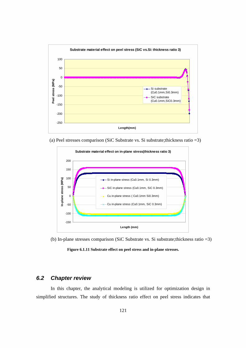
121
Substrate material effect on peel stress (SiC vs.Si: thickness ratio 3)
-250
-200
-150
-100
-50
0
50
100
Length(mm)
Peel
stre
ss (M
Pa)
Si substrate(Cu0.1mm,Si0.3mm)SiC substrate(Cu0.1mm,SiC0.3mm)
(a) Peel stresses comparison (SiC Substrate vs. Si substrate;thickness ratio =3)
Substrate material effect on in-plane stress(thickness ratio 3)
-150
-100
-50
0
50
100
150
200
Length (mm)
In-p
lane
str
ess
(MPa
)
Si in-plane stress (Cu0.1mm, Si 0.3mm)
SiC in-plane stress (Cu0.1mm, SiC 0.3mm)
Cu in-plane stress ( Cu0.1mm Si0.3mm)
Cu in-plane stress (Cu0.1mm, SiC 0.3mm)
(b) In-plane stresses comparison (SiC Substrate vs. Si substrate;thickness ratio =3)
Figure 6.1.11 Substrate effect on peel stress and in-plane stresses.
6.2 Chapter review
In this chapter, the analytical modeling is utilized for optimization design in
simplified structures. The study of thickness ratio effect on peel stress indicates that
122
thinner copper film leads to lower maximum tensile stress and smaller peel stress active
zone. The critical contact size is introduced as double of the peel stress active zone.
Smaller contacts result in non-zero stress on the whole contact area, which should be
avoid in designs. If all the other module parameters remains the same, thicker copper film
has bigger critical contact size due to its larger peel stress active zone. Peel stress is not
sensitive to the substrate and film length ratio, if the copper film length remains the same.
However, if the substrate length remains the same and copper length decreases to a
certain level, the in-plane stress in substrate will not reach to its high plateau value.
Therefore, for narrow copper traces, the in-plane stress in substrate can be decreased.
Adhesion materials directly effect the peel stress. Aluminum and Chromium are
investigated as two candidates. Al have lower peel stress due to its lower Young’s
modulus than Cr. Substrate material effect on peel stress and in-plane stress are also
investigated. SiC and Si are two substrate materials. Peel stress is not effect much by
substrate materials. However, in-plane stress in SiC is higher than Si due to higher
Young’s modulus in SiC.
Analytical modeling provides clear trends of the mechanical behavior of the
system. It is an effective tool for design. However, up to this time, experimentally
measure the thermally introduced stresses have not been fully solved, especially in
complicated structure. Finite Element Modeling is the available method to calibrate the
modeling results. Therefore, it is easier to predict and chose the better design than to
quantify the values of thermo-mechanical stresses. In addition to that, all the modeling in
this study assume that the film and substrate are under the uniform thermal loading due to
the smaller temperature gradients between film and substrate. For improved study, FEM
can import the temperature distributions from the thermal simulation and simulate the
stress distributions based on these imported temperature distribution. All the materials are
assumed to be isotropic. The adhesion layer is much thinner than the main material layers.

123
Chapter 7: Summary and future work
7.1 Summary
In integrated power modules, copper deposition is on brittle substrates such as
silicon or ceramic. Different from thin films, thicknesses of copper deposition in IPEMs
are in the range above 75µm. Under high current working conditions, those thick films in
IPEMs have unknown failure modes and reliability. This study starts with the literature
review of interface qualities. After that, residual stress and thermal stress are investigated
in consequence. Power cycling and temperature cycling tests are designed and carried out.
The failure modes in integrated modules under high current working conditions and their
driving forces are identified. The analytical modeling is utilized as design tools to
optimize the geometry and material parameters for higher failure resistance.
The critical interface in Embedded Power modules is copper-silicon interface. Since
there is a thin layer of aluminum on top of silicon, copper-silicon interface is actually the
material combination of copper-aluminum-silicon. The interface between Copper-
aluminum processed by planar interconnection technology has 30nm sputtered Ti layer
and a 300nm Cu seed layer before the electroplating process. Generally, this inter-
metallic interface should have good adhesion, if there is no contamination on the
interface. For integrated passive modules, the chemical reaction between ceramic
substrates and sputtered Ti and Cu is unknown. Copper-ceramic interface processed by
planar technology is mainly bonded by surface mechanical locking of compound bonding.
The unmatched surface roughness may cause voids on interface. This copper-ceramic
interface is not expected to have as good adhesion as an inter-metallic interface. Good
interface adhesion has a higher delamination strength, which helps modules to operate
under severe conditions.
Intrinsic residual stress is investigated theoretically and experimentally. Residual
stress is the stress induced by processing. There is not a uniform theory to explain the
cause of the residual stress. The possible reason is that the mismatch of the lattice causes
the residual stress. In the thin film industry, the intrinsic residual stress sometime can
reach up to a few Gpa. It plays an important role for module reliability. In this study, the
124
residual stress is measured in a simplified copper-glass structure. The curvatures of glass
after copper electroplating process are measured by a Dektak surface profile machine.
Residual stress is calculated by a modified Stoney equation based on these surface
curvature. The results indicate that the residual stress is much smaller than the thermally
induced stresses. Therefore, the residual stresses induced by planar process are ignored
during the investigation of thermo-mechanical stresses. The electroplating process
temperature, around 20°C, is assumed to be the residual stress free point.
Thermo-mechanical stresses are investigated extensively by analytical modeling and
FEM simulation. The calculation and simulation results are compared. Four types of
thermo-mechanical stresses, Von Mises, peel stress, in-plane stress and shear stress, are
related to different failures. Von Mises is suitable to predict ductile material fractures
such as copper. Once the Von Mises reaches beyond the yield stresses of a ductile
material, the design need to be modified. The yield stress of electroplating copper is
about 300Mpa. Under normal working temperatures, Von Mises will not exceed copper
yield stress. Shear stress is a commonly studied indicator for delamination or other
failures. Shear stress is only dependent on the magnitude of the temperature difference.
However, the peel stress is dependent on the magnitude and sign of the temperature
difference, as well as the mechanical and geometrical parameters of the strips. Therefore,
peel stress is given more attention in this study as the direct indicator of delamination. In-
plane stress in brittle materials is the failure indicator for substrate cracks. Bi-material
structure with adhesive layer is adopted for Embedded Power module modeling since
only one side of silicon has copper deposition. Tri-material structure without an adhesive
layer is adopted for the integrated passive modules because there are copper layers on
both sides of the ceramics. The adhesive Ti layer is too thin to be modeled. It turns out
that analytical modeling is an effective tool for geometry and material parameters design.
However, FEM simulation is necessary for complicated structures. According to
simulation results of complicated structures close to practical applications, the highest
stress spots are always located between copper-silicon or copper-ceramic interfaces.
In order to verify the simulation results, a power cycling test and temperature
cycling tests are carried out. A temperature cycling lifetime is longer than a power
cycling lifetime by current failure criteria. From room temperature to high temperature
125
power cycling, the delamination and cracks through whole silicon chips are the major
failure modes. This is due to the tensile peel stress and tensile in-plane stress in the
silicon layer. From below room temperature to room temperature power cycling, spalling
was detected. This is probably due to the high tensile peel stress on the edges. The
contact pattern effect on the module maximum working temperature is investigated.
Enlarged contact patterns and multiple contact areas ensure a better connection and
redundancy of thermal and electrical paths. If contact patterns are smaller than peel stress
active zone, the whole contact is subjected to peel stress. It has been experimentally
proven that peel stress is a very important failure indicator for delamination, and in-plane
stress is the failure indicator for brittle substrate cracks.
Since delamination and substrate cracks are frequently observed failure modes for
integrated power electronics modules, minimizing peel stress and in-plane stress are two
goals during geometry design and material selection. Analytical tools are utilized in the
theoretical optimization design of IPEMs. In Embedded Power modules, peel stress is
sensitive to the thickness ratio. Assuming that the substrate thickness is the same, a
thicker copper may lead to a higher maximum tensile peel stress. For integrated passive
modules, a tri-material structure is used since there are copper deposition on both sides of
ceramics. In-plane stress is sensitive to the thickness ratio. If the copper thickness is the
same, a thinner ceramics will result in a higher in-plane stress. These are basic design
guidelines for high failure resistance modules.
7.2 Future work
Understanding and identifying the planar metallization failure modes enable the
optimization of the module design to achieve high resistance to the failure and improve
reliability in the system level. However, experimentally quantifying the failure strengths
in either the Embedded Power modules or the integrated passive modules is lacking. For
example, to predict delamination, tensile peel stress and interface adhesion strength needs
to be known. If peel stress is greater than the adhesion strength, delamination will not
happen. Peel stress has been theoretical modeled in this study. However, experimentally
measuring the peel stress has not been solved up to this time. Secondly, adhesion strength
126
has not been quantified by these experiments. Further more, control of interface quality
still needs to be improved.
The failure and reliability criteria for brittle materials are governed by both the applied
stress and a length-scale parameter, such as defect size or layer thickness. To prevent
brittle material cracks, in-plane stress needs to be smaller than the materials’ fracture
strength. Similar to peel stress, in-plane stress has, so far, not been experimentally
measured so far. Brittle materials used in IPEMs are silicon chips or commercial
available ceramic tiles. Defects, introduced during shipping and handling are hard to
control and measure. Measuring fracture strengths of these materials, especially for
ceramic tiles due to their thin thickness, will be a challenging task in the future.

127
References 1. Energy Information Administration (EIA) reports on 2004, U.S. department of
energy, Washington D.C. 20585, release on April 14, 2004
2. National Committee on Power Electronics, Report on Power Electronics and Global
Competitiveness, EPRI, 1992
3. Lee, F.C.; van Wyk, J.D.; Liang, Z.X.; Chen, R.; Wang, S.; Lu, B.; An integrated
power electronics modular approach: concept and implementation; Power Electronics
and Motion Control Conference, 2004, IPEMC 2004. The 4th International Volume 1,
2004 pp1-13 Vol.1
4. van Wyk, J.D.; Ferreira, J.A.; Some present and future trends in power electronics
converters; in proceedings IEEE IECON, 9-13 November 1992, Vol.1, pp9-18
5. Hofsajer, I.W.; Ferreira, J.A.; van Wyk, J.D.; Smit, M.C.; Integrated technology and
performance for multi-kilowatt power electronic converters-An Evaluation; in
proceeding IEEE IECON, 15-19 November 1993, Vol.2, pp779-784.
6. Ferreira, J.A.; Hofsajer, I.W.; van Wyk, J.D.; Exploiting the third dimension in power
electronics packaging; in proceedings of IEEE APEC, 23-27 February 1997, Vol. 1,
pp419-423
7. van Wyk, J.D.; Lee, F.C.; Boroyevich D.; Power electronics technology: present
trends and future developments; in scanning the issue, proceedings of the IEEE,
vol.89, no.3, 2001, pp223-226
8. Stockmeier, T.; Tursky, W.; Present and future trends in power electronic converters;
in proceeding of CPES seminar 2000, Blacksburg, pp3-9
9. I.W. Hofsajer, J.D. van Wyk, J.A.Ferreira, Functional component integration in a
multi-kilowatt resonant converter, European Power Electronics Conference Record,
EPE 93, Brighton, UK, September 1993, vol.2, pp.125-130
10. J.T. Strydom, J.D. van Wyk, J.A.Ferreira, Some limits of integrated LCT modules for
resonant converters at 1MHz, IEEE Transactions on Industry Applications, Vol. 37,
No.2, May/June 2001, pp.820-828
128
11. L.Zhao, J.T. Strydom, J.D. van Wyk, An integrated LC resonant module for high
power soft-swtiching converter, Power Electronics Specialists Conference, PESC
2001, Vol.4, June 2001, pp.1944-1948
12. Fred C. Lee, Dengming Peng; Power Electronics Building Block and System
Integration; Power Electronics and Motion Control Conference, 2000, Proceedings,
PIEMC 2000, the Third International Volume 1, 15-18 Aug. 2000 pp: 1-8 vol. 1
13. Rao R. Tummala, Fundamentals of Microsystems Packaging, McGRAW Hill, pp346-
347
14. Syd R. Wilson, Clarence J. Tracy, John L. Freeman, Jr.; Handbook of multilevel
metallization for integrated circuits—materials, technology, and applications; Noyes
publications, Park Ridge, New Jersey, USA; pp822-834
15. Analog Devices, “BGA background”, ADI home> Embedded Processing &DSP>
Products and Data Sheets> Packaging and Numbering > Ball Grid Array
16. Fred C. Lee, Peter Barbosa, “The state-of-the-art power electronics technologies and
future trends”, Transmission and Distribution Conference and Exposition,
2001IEEE/PES, Volume: 2, 28Oct.-2Nov.2001 Pages: 1188 - 1193 vol.2
17. Eberhard Waffenschmidt, J.A.Ferreira, “Embedded passives integrated circuits for
power converters”, in Proceedings of IEEE Power Electronics Specialists Conference,
2002, pp.12-17, vol.1
18. L.Y. Zhao, J.D. van Wyk; Frequency-domain modeling of integrated electromagnetic
power passives by a generalized two-conductor transmission structure; IEEE
Transactions on circuit and systems-I: regular papers, vol. 51, No. 10, Nov 2004
19. Chen Rengang; Integrated EMI filters for switch mode power supplies; Dissertation
submitted to Virginia Polytechnic Institute and State University for Ph.D degree in
Electrical engineering; Nov 2004; pp22-27.
20. M.C.Shaw, High-performance packaging of power electronics, MRS bulletin, January
2003
21. Johannes Juul Mikkelsen, “Failure analysis on direct bonded copper substrates after
thermal cycle in different mounting conditions”, proceedings of power conversion
PCIM, Nueremberg, Germany, 2001 pp467-471

129
22. Mohnish Charan, Rosalyn A. Sayer, Ning Zhu, J.D. van Wyk, Michael C.Shaw;
Reliability of HDI substrates—Strength, Toughness and defect size relationships;
Proceedings of CPES seminar 2005; Blacksburg, VA, April 2005; pp 138-141
23. David W. Richerson, Modern Ceramic Engineering-properties, processing, and use in
design; Published in 2006 by CRC Press, Taylor & Francis Group; Fl; pp94-105
24. Ayal de S. Jayatilaka; Fracture of engineering brittle materials; Applied science
publishers LTD; England: 1979; pp49
25. V.D. Frenchette; Failure analysis of brittle materials; the American ceramic society,
Inc, Westerville, Ohio; c1990; Advances in ceramics, volume 28; pp1- 59
26. Donald M. Mattox; Handbook of physical vapor deposition (PVD) processing; Noyes
Publications; Westwood, New Jersey, USA, 1998; pp57-61
27. Milton Ohring, “Materials science of thin films---Deposition & structure”, Second
Edition, Academic Press, pp767-768
28. Dr. Jurgen Schulz-Harder, Alexander Rogg, Dr. Karl Exel; Recent developments of
DBC substrate for high resolution requirements; Proceedings of IMAPS 2004
29. Donald M. Mattox; Handbook of physical vapor deposition (PVD) processing; Noyes
Publications; Westwood, New Jersey, USA, 1998; pp343-396
30. Ronald A. Powell, Stephen M. Rossnagel; PVD for microelectronics: Sputter
deposition applied to semiconductor manufacturing; San Diego Academic Press,
c1999; pp1-3
31. K.Ramkumar, S.K.Ghosh, A.N.Saxena; Aluminum based multilevel metallizations in
VLSI/ULSICs; in handbook of multilevel metallization for integrated circuits, pp97-
201
32. Ronald A. Powell, Stephen M. Rossnagel; PVD for microelectronics: Sputter
deposition applied to semiconductor manufacturing; San Diego Academic Press,
c1999; pp292-295
33. V.M.Dubin, C.H.Ting, R.Cheng, R.Lee, S.Chen; copper plating techniques for ULSI
metallization; Advanced MetalliZation and interconnect systems for ULSI
applications in 1997; editors Robin Cheung, Jeffery Klein, Kazuo Tsubouchi,
masanori murakami, nobuyoshi kobayashi; Material Research Society, Warrwndale,
Pennsylvania; pp405-411
130
34. V.M. Dubin, E.H.Bernard, D.Schonauer, J.Bertrand; Cleaning in Cu metallization
technology; Advanced MetalliZation and interconnect systems for ULSI applications
in 1997; editors Robin Cheung, Jeffery Klein, Kazuo Tsubouchi, masanori murakami,
nobuyoshi kobayashi; Material Research Society, Warrwndale, Pennsylvania; pp421-
426
35. Ronald A. Powell, Stephen M. Rossnagel; PVD for microelectronics: Sputter
deposition applied to semiconductor manufacturing; San Diego Academic Press,
c1999; pp307-310
36. S.R. Wilson, D.Weston, M.Kottke; The effects of Si addition on the properties of
AlCu films used in multilevel metal systems; Materials research society Symposium
proceedings; volume 181; Advanced metallizations in microelectronics; editors
Avishay Katz, Shyam P. Murarka, Ami Appelbaum; pp545-548
37. G. Cui, M.Lane, K.Vijayamohanan, G. Ramanath; Interfacial adhesion of Cu to self-
assembled monolayers on SiO2; Material research society symposium proceedings
Vol.695 @ 2002 materials research society; pp329-334
38. R.Mitra, A.Madan, R.A.Hoffman, W.A.Chiou, J.R.Weertman; Effect of annealing on
microstructure and properties of Al-Ti Multilayered films; Materials research society
symposium proceedings volume 594; Thin films-stresses abd mechnical properties
VIII; Symposium held November 29-December 3, 1999, Boston, Massachusetts,
U.S.A; Editors Richard Vinci, Oliver Kraft, Neville Moody, Paul Besser, Edward
Shaffer II; pp43-48
39. Christopher A.Apblett, Peter J. Ficalora; Effect of hydrogen on thin Cu/Ti and Cu
films; Materials research society symposium proceedings Vol.239 @ 1992; pp99-106
40. D.M. Mattox; Handbook of physical vapor deposition processing-film formation,
adhesion, surface preparation and contamination control; Society of vacuum coaters;
Albuquerque, New Mexico; pp625.
41. Yong Xiang, Xi Chen and Joost J.Vlassak; The mechanical properties of electroplated
Cu thin films measured by means of the Bugle Test Technique; Material research
society symposium proceedings Vol.695 @ 2002 materials research society; pp189-
194
131
42. Yong Xiang, Joost J. Vlassak, Maria T. Perez-Prado, Ting Y. Tsui, Andrew J.
McKerrow; The effect of passivation layer and film thickness on the mechanical
behavior of freestanding electroplated Cu thin films with constant microstructure;
Materials Research Society Symposium Proceedings Vol.795 @ 2004; pp417-422
43. Jin Won Choi, Tae Sung Oh; Effects of mechanical properties of metal films on the
adhesion strength of Cr/Polyimide interfaces; Materials Research Society Symposium
Proceedings Vol.436 @ 1997; pp121-126
44. I.S. Park, Jin Yu, Y.B. Park; Peel Strength in the Cu/Cr/Polyimide System; Materials
Research Society Symposium Proceedings Vol.436 @ 1997; pp133-138
45. R.Spolenak, C.A.Volkert, K.Takahashi, S.Fiorillo, J.Miner, W.L.Brown; Mechanical
properties of electroplated copper thin films; Materials research society symposium
proceedings volume 594; Thin films-stresses and mechanical properties VIII;
Symposium held November 29-December 3, 1999, Boston, Massachusetts, U.S.A;
Editors Richard Vinci, Oliver Kraft, Neville Moody, Paul Besser, Edward Shaffer II;
pp63-68
46. W.D.Nix; Mechanical properties of thin films; Metallurgical transactions, vol. 20A,
November 1989, pp2217-2245
47. D.M. Mattox; Handbook of physical vapor deposition processing-film formation,
adhesion, surface preparation and contamination control; Society of vacuum coaters;
Albuquerque, New Mexico; pp510-516
48. Milton Ohring, “Materials science of thin films---Deposition & structure”, Second
Edition, Academic Press, pp751
49. Milton Ohring, “Materials science of thin films---Deposition & structure”, Second
Edition, Academic Press, pp723-726
50. Z.B.Zhao, J.Hershberger, S.M.Yalisove, J.C. Bilello; On the measurement of residual
stress in thin films; Material research society symposium proceeding vol.505 @ 1998;
pp519-525
51. Milton Ohring, “The materials science of thin films” Second Edition, Academic
Press; 1992; P429-431
52. William H. Safranek, “The Properties of Electrodeposited Metals and Alloys”, A
handbook, Second Edition pp107-133
132
53. S.H.Brongersma, E.Richard, I.Vervoort, and K.Maex, “Stress in Electrochemically
Deposited Copper”, Stress Induced Phenomena in Metallization Fifth international
Workshop, Stuttgart, Germany, pp249-256, June1999
54. Ying Feng Pang; Assessment of thermal behavior and development of thermal design
guidelines for integrated power electronics modules; Dissertation submitted to
Virginia Polytechnic Institute and State University for Ph.D degree in Mechanical
engineering; Jan 2005; Chapter 3, 47.
55. Kang Ping Wang, Yonggang Young Huang, Abihijit Chandra, and Kai Xiong Hu;
Interfacial shear stress, peeling stress, and die cracking stress in trilayer electronic
assemblies; IEEE transactions on components and packaging technologies; vol. 23;
June 2000
56. William D. Brown; Advanced electronic packaging with emphasis on multi-chip
modules; IEEE Press series on Microelectronic systems; The institute of electrical
and electronics engineers, Inc., New York; 1999; 235-239
57. Donald M. Mattox; Handbook of Physical Vapor Deposition (PVD) Processing, Film
formation, adhesion, surface preparation and contamination control; Society of
vacuum coaters; Albuquerque, New Mexico; Noyes publications; Westwood, New
Jersey, USA; 1998; pp619-620
58. Chen, C.P, Leipold, M.H; Fracture Toughness of Silicon; American Ceramic Society
Bulletin; Vol.59, No. 4, pp.469-472; April 1980
59. Duk-Ho Cho, Young-Wook Kim, Wonjoong Kim; Strength and fracture toughness of
in situ-toughened silicon carbide; Journal of material science, Volume 32, Number
18; Jan 1997; pp.4777-4782
60. S.P. Timoshenko, “Analysis of Bi-Metal Thermostats”, Journal of the Optical Society
of America, Vol. 11, pp.233-255, 1925
61. E.Suhir, “Stresses in Adhesively Bonded Bi-Material Assemblies used in Electronic
Packaging,” Proceedings of the Electrnic Packaging Materials Science Symposium II,
Palo Alto, California, April 15-18, pp133-138, 1986
62. Tummala, R., Rymaszewski, E.; Microelectronics packaging handbook, van
Nostrand, 1988
133
63. H.B.Mirman, effecgt of peeling stresses in biomaterial assembly; ASME Journal of
Electronic packaging; vol.113, pp.431-433; 1991
64. K. P. Wang, Y. Y. Huang, A. Chandra, and K. X. Hu; Interfacial shear stress, peeling
stress, and die cracking stress in trilayer electronic assemblies; IEEE Transactions on
Components and Packaging Technologies; vol. 23; June 2000
65. J.W.Hutchinson and Z.Suo; Mixed Mode Cracking in Layered Materials; Advanced
in Applied Mechanics, vol.29; pp.63-191, 1992
66. S.Y.Lee, N.Zhu, W.G.Odendaal, J.D.van Wyk; Power cycling test for passive
integrated power electronic modules; Proceedings of CPES seminar2003; Blacksburg,
VA, April 2003; pp493-498
67. Curamik research experiences and resources; Material is from on-site presentation.

134
Appendix A: E. Suhir’s stress model
E. Suhir's Stress Model
Temperature difference ∆T 80:=
Half of the assembly length l 0.001:=
poisson's ratio Young's Modulus Thickness CTE
υ1 0.29:= E1 115 109⋅:= h1 0.3:= mm α1 8.9 10 6−
⋅:=
mm υ2 0.343:= E2 110 109
⋅:= h2 0.1:= α2 16.4 10 6−⋅:=
υa 0.35:= Ea 8.9 109⋅:= ha 10 10 3−⋅:= mm
Axial compliances
λ11 υ1−
E1 h1⋅:= λ2
1 υ2−
E2 h2⋅:= λ12 λ1 λ2+:=
Interfacial compliances
κ123
1 υ1+
E1⋅ h1⋅:= κ2
23
1 υ2+
E2⋅ h2⋅:= κa
43
1 υa+
Ea⋅ ha⋅:=
κ κ1 κ2+ κa+( ) 10 3−⋅:=
h h1 h2+:=
Flexural rigidities
D1E1 h13⋅
12 1 υ1−( )⋅:= D2
E2 h23⋅
12 1 υ2−( )⋅:= D D1 D2+:=
λ112
h12
D1h22
D2+ 3
h2
D⋅+
⎛⎜⎝
⎞
⎠⋅ 103
⋅:=
kλ
κ:=
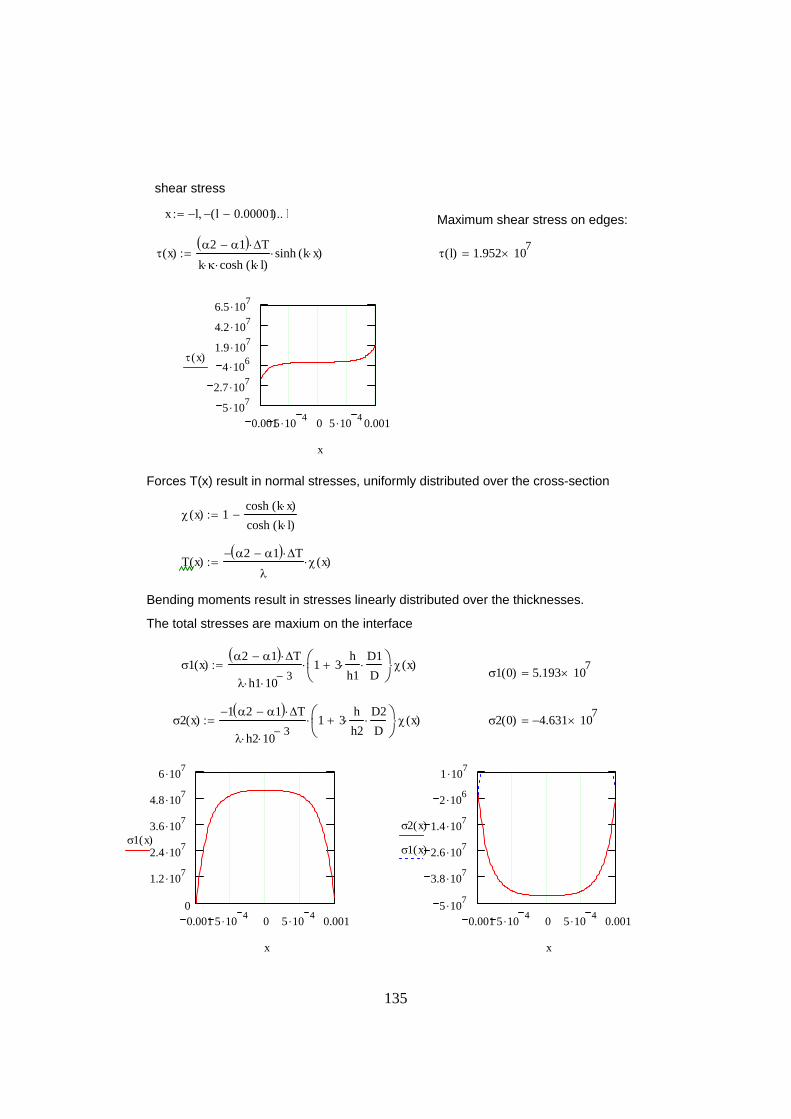
135
shear stress
x l− l 0.00001−( )−, l..:= Maximum shear stress on edges:
τ x( )α2 α1−( ) ∆T⋅
k κ⋅ cosh k l⋅( )⋅sinh k x⋅( )⋅:= τ l( ) 1.952 107
×=
0.0015 .10 4 0 5 .10 4 0.0015 .107
2.7 .1074 .106
1.9 .1074.2 .1076.5 .107
τ x( )
x
Forces T(x) result in normal stresses, uniformly distributed over the cross-section
χ x( ) 1cosh k x⋅( )cosh k l⋅( )
−:=
T x( )α2 α1−( )− ∆T⋅
λχ x( )⋅:=
Bending moments result in stresses linearly distributed over the thicknesses.
The total stresses are maxium on the interface
σ1 x( )α2 α1−( ) ∆T⋅
λ h1⋅ 10 3−⋅
1 3hh1⋅
D1D
⋅+⎛⎜⎝
⎞⎠
⋅ χ x( )⋅:= σ1 0( ) 5.193 107
×=
σ2 x( )1− α2 α1−( ) ∆T⋅
λ h2⋅ 10 3−⋅
1 3hh2⋅
D2D
⋅+⎛⎜⎝
⎞⎠
⋅ χ x( )⋅:= σ2 0( ) 4.631− 107×=
0.001 5 .10 4 0 5 .10 4 0.0010
1.2 .107
2.4 .107
3.6 .107
4.8 .107
6 .107
σ1 x( )
x
0.001 5 .10 4 0 5 .10 4 0.0015 .107
3.8 .107
2.6 .107
1.4 .107
2 .106
1 .107
σ2 x( )
σ1 x( )
x
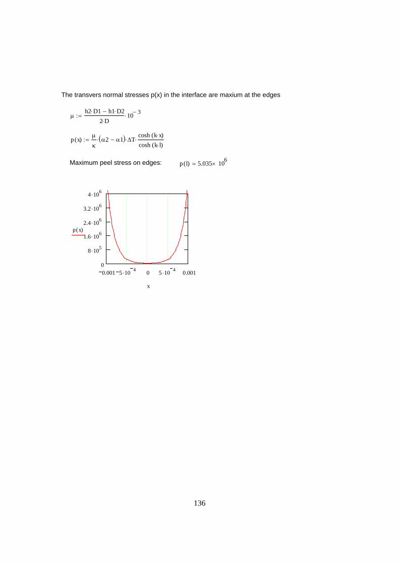
136
The transvers normal stresses p(x) in the interface are maxium at the edges
µh2 D1⋅ h1 D2⋅−
2 D⋅10 3−⋅:=
p x( )µ
κα2 α1−( )⋅ ∆T⋅
cosh k x⋅( )cosh k l⋅( )⋅:=
Maximum peel stress on edges: p l( ) 5.035 106×=
0.001 5 .10 4 0 5 .10 4 0.0010
8 .105
1.6 .106
2.4 .106
3.2 .106
4 .106
p x( )
x
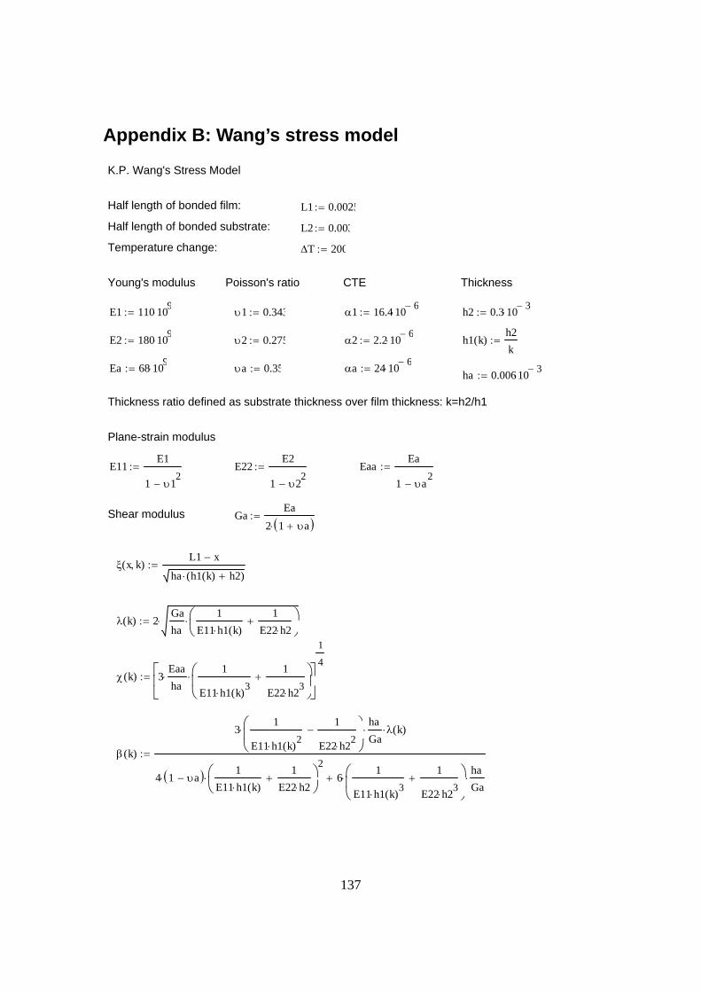
137
Appendix B: Wang’s stress model
K.P. Wang's Stress Model
Half length of bonded film: L1 0.0025:=
Half length of bonded substrate: L2 0.003:=
Temperature change: ∆T 200:=
Young's modulus Poisson's ratio CTE Thickness
E1 110 109⋅:= υ1 0.343:= α1 16.4 10 6−
⋅:= h2 0.3 10 3−⋅:=
E2 180 109⋅:= υ2 0.275:= α2 2.2 10 6−⋅:= h1 k( )h2k
:=
Ea 68 109⋅:= υa 0.35:= αa 24 10 6−⋅:= ha 0.006 10 3−⋅:=
Thickness ratio defined as substrate thickness over film thickness: k=h2/h1
Plane-strain modulus
E11E1
1 υ12
−
:= E22E2
1 υ22
−
:= EaaEa
1 υa2
−
:=
Shear modulus GaEa
2 1 υa+( )⋅:=
ξ x k,( )L1 x−
ha h1 k( ) h2+( )⋅:=
λ k( ) 2Gaha
1E11 h1 k( )⋅
1E22 h2⋅
+⎛⎜⎝
⎞⎠
⋅⋅:=
χ k( ) 3Eaaha
⋅1
E11 h1 k( )3⋅
1
E22 h23⋅
+⎛⎜⎝
⎞
⎠⋅⎡
⎢⎣
⎤⎥⎦
1
4:=
β k( )
31
E11 h1 k( )2⋅
1
E22 h22⋅
−⎛⎜⎝
⎞
⎠⋅
haGa⋅ λ k( )⋅
4 1 υa−( )⋅1
E11 h1 k( )⋅
1E22 h2⋅
+⎛⎜⎝
⎞⎠
2⋅ 6
1
E11 h1 k( )3⋅
1
E22 h23⋅
+⎛⎜⎝
⎞
⎠⋅
haGa⋅+
:=
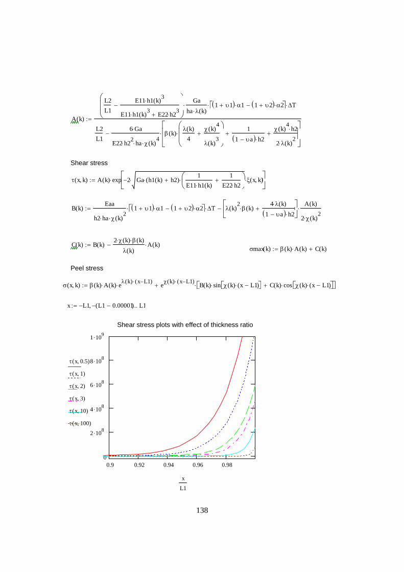
138
A k( )
L2L1
E11 h1 k( )3⋅
E11 h1 k( )3⋅ E22 h23
⋅+−
⎛⎜⎜⎝
⎞
⎠
Gaha λ k( )⋅⋅ 1 υ1+( ) α1⋅ 1 υ2+( ) α2⋅−⎡⎣ ⎤⎦⋅ ∆T⋅
L2L1
6 Ga⋅
E22 h22⋅ ha⋅ χ k( )
4⋅
β k( )λ k( )
4χ k( )
4
λ k( )3
+⎛⎜⎜⎝
⎞
⎠⋅
11 υa−( ) h2⋅
+χ k( )
4h2⋅
2 λ k( )2
⋅
+⎡⎢⎢⎣
⎤⎥⎥⎦
⋅−
:=
Shear stress
τ x k,( ) A k( ) exp 2− Ga h1 k( ) h2+( )⋅1
E11 h1 k( )⋅
1E22 h2⋅
+⎛⎜⎝
⎞⎠
⋅⋅ ξ x k,( )⋅⎡⎢⎣
⎤⎥⎦
⋅:=
B k( )Eaa
h2 ha⋅ χ k( )2
⋅
1 υ1+( ) α1⋅ 1 υ2+( ) α2⋅−⎡⎣ ⎤⎦⋅ ∆T⋅ λ k( )2β k( )⋅
4 λ k( )⋅
1 υa−( ) h2⋅+⎡
⎢⎣
⎤⎥⎦
A k( )
2 χ k( )2
⋅
⋅−:=
C k( ) B k( )2 χ k( )⋅ β k( )⋅
λ k( )A k( )⋅−:=
σmax k( ) β k( ) A k( )⋅ C k( )+:=
Peel stress
σ x k,( ) β k( ) A k( )⋅ eλ k( ) x L1−( )⋅⋅ eχ k( ) x L1−( )⋅ B k( ) sin χ k( ) x L1−( )⋅⎡⎣ ⎤⎦⋅ C k( ) cos χ k( ) x L1−( )⋅⎡⎣ ⎤⎦⋅+⎡⎣ ⎤⎦⋅+:=
x L1− L1 0.00001−( )−, L1..:=
0.9 0.92 0.94 0.96 0.980
2 .108
4 .108
6 .108
8 .108
1 .109
τ x 0.5,( )
τ x 1,( )
τ x 2,( )
τ x 3,( )
τ x 10,( )
τ x 100,( )
x
L1
Shear stress plots with effect of thickness ratio
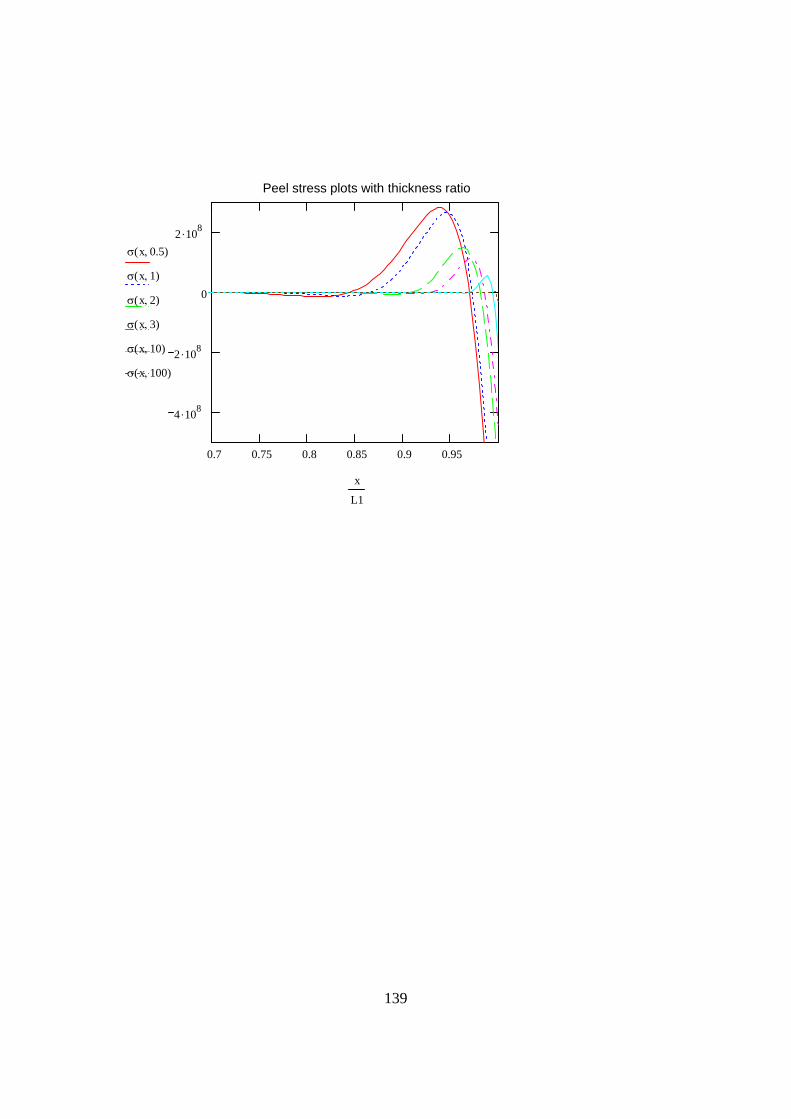
139
0.7 0.75 0.8 0.85 0.9 0.95
4 .108
2 .108
0
2 .108
σ x 0.5,( )
σ x 1,( )
σ x 2,( )
σ x 3,( )
σ x 10,( )
σ x 100,( )
x
L1
Peel stress plots with thickness ratio
140
Appendix C: Related publications 1. N. Zhu, S.Y.Lee, J.D. van Wyk, W.G. Odendaal, Z.X.Liang, “Thermal Stress and
Intrinsic Residual Stress in Embedded Power Modules”, Conference Record of 2003
IEEE Industry Applications Conference, 38th IAS Annual Meeting, Salt Lake City;
Volume 2, 12-16 Oct.2003; pp1244-1250.
2. N. Zhu, J.D. van Wyk, Z.X.Liang, “Thermal-Mechanical Stress Analysis in Embedded
Power Modules”, Proceedings, IEEE Power Electronics Specialists Conference 2003,
35th annual meeting, June, Aachen Germany, pp4503-4508
3. N.Zhu, J.D.van Wyk, F. Wang , “Modeling and design of integrated parallel resonant
transformer”, Proceedings, IEEE Power Electronics Specialists Conference 2005, 36th
annual meeting, June12-16, Recife, Brazil;
4. N.Zhu, J.D. van Wyk, Z.X. Liang, A study of thermal stress and intrinsic stress in
planar metallization for integrated power modules, IEEE Transactions on Industry
Applications, Vol. 41, No.6, Nov/Dec 2005, pp1603-1611
5. N.Zhu, J.D.van Wyk, Z.X.Liang; Thermo-mechanical Stress Analysis for Planar
Metallization in Integrated Power Electronics Modules; Proceedings of CIPS 2006;
June, Italy.
6. N. Zhu, J.D.van Wyk, W.G.Odendaal, J.N.Calata, “Measurement and Calculation of
Residual Stress Between Substrate and Copper Deposition in Integrated Passive
Modules”, Proceedings, CPES seminar2003, pp554-558.
7. N. Zhu, J.D. van Wyk, Z.X.Liang, “Increased Functional Integration of Embedded
Power Technology by Embedding the Decoupling Capacitor”, Proceedings, CPES
seminar2004, Blacksburg, VA, pp154-158
8. N.Zhu, J.D.Van Wyk, Z.X.Liang, “Thermo-mechanical Stress Investigation and
Power Cycling Test for Embedded Power Modules with Planar Metallization on
Brittle Substrates”, Proceedings, CPES seminar 2005, Blacksburg, April 23-25.
9. Y.Pang, E.P.Scott, N.Zhu, J.D.van Wyk, “Assessment of Thermo-mechanics for an
Integrated Power Electronics Switching Stage”, Conference Record of 2004 IEEE
Industry Applications Conference, 39th IAS Annual Meeting, Seatle; pp2309-2314

141
10. Seung-Yo Lee, Ning Zhu, W.G.Odendaal, J.D.van Wyk, “Power Cycling Tests for
Passive Integrated Power Electronic Modules”, Proceedings, CPES seminar 2003,
pp493-498
11. M.Charan, R.A.Sayer, N. Zhu, J.D.van Wyk, M.C. Shaw, Reliability of HDI
Substrates – Strength, Toughness and Defect Size Relationships, Proceeding, CPES
seminar 2005, pp138-141
142
Vita Ning Zhu received her B.S. degree of electrical engineering from Wuhan University,
China, in 1997. She received her M. S. degree of the same major from Wuhan University,
China, in 2000. Since 2001 utill 2006, she has been a PhD student and a graduate
research assistant in Center for Power Electronics Systems (CPES), Virginia Polytechnic
Institute and State University.
Her research interests include power electronics circuits and modeling, advanced
power circuit packaging technologies, power passive integration, thermo-mechanical
studies and reliability analysis.