Advanced front side metallization for crystalline silicon
23
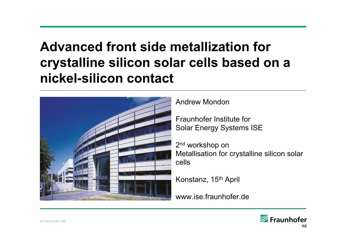
© Fraunhofer ISE Advanced front side metallization for crystalline silicon solar cells based on a nickel-silicon contact Andrew Mondon Fraunhofer Institute for Solar Energy Systems ISE 2 nd workshop on Metallisation for crystalline silicon solar cells Konstanz, 15 th April www.ise.fraunhofer.de
Transcript of Advanced front side metallization for crystalline silicon
© Fraunhofer ISE
Advanced front side metallization for crystalline silicon solar cells based on a nickel-silicon contact
Andrew Mondon
Fraunhofer Institute for Solar Energy Systems ISE
2nd workshop onMetallisation for crystalline silicon solar cells
Konstanz, 15th April
www.ise.fraunhofer.de
© Fraunhofer ISE
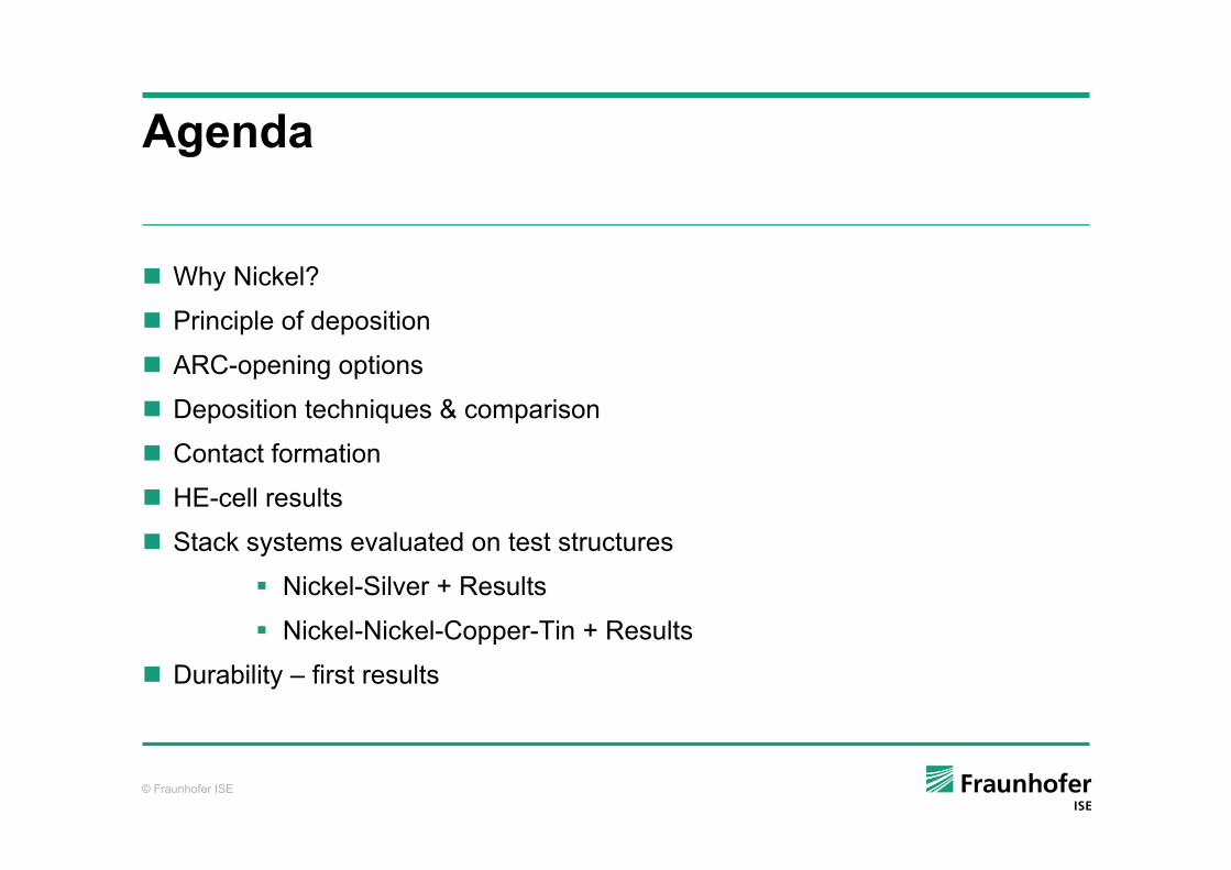
Agenda
Why Nickel?
Principle of deposition
ARC-opening options
Deposition techniques & comparison
Contact formation
HE-cell results
Stack systems evaluated on test structures
Nickel-Silver + Results
Nickel-Nickel-Copper-Tin + Results
Durability – first results
© Fraunhofer ISE
3
Ng, K.K., "Barrier heights and contact resistances: Metal/Si", Properties ofSilicon, Chapter 20 1987, pp. 799-845.
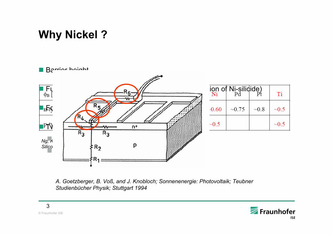
Why Nickel ?
Barrier height
Two possible functions:
Contact formation/seed layer
Barrier layer to prevent copper diffusion
Full area contact with low contact resistance (formation of Ni-silicide)
Formation of nickel silicide also raises adhesion
A. Goetzberger, B. Voß, and J. Knobloch; Sonnenenergie: Photovoltaik; Teubner Studienbücher Physik; Stuttgart 1994
© Fraunhofer ISE
4
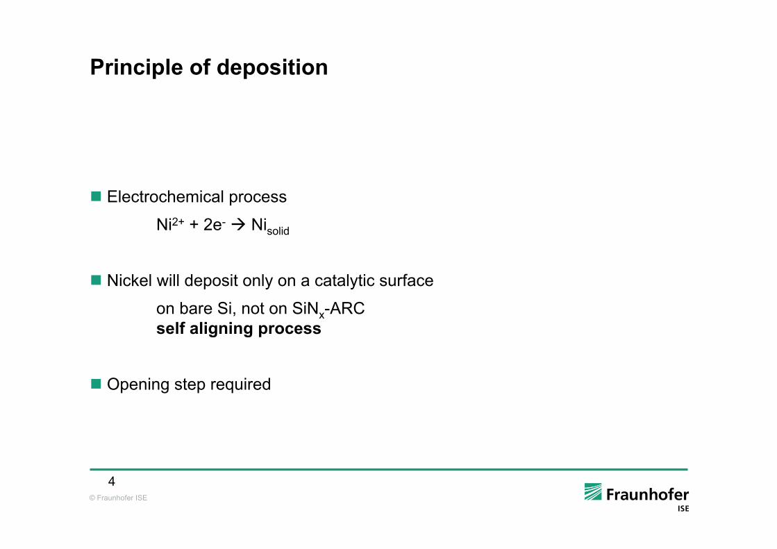
Principle of deposition
Electrochemical process
Ni2+ + 2e- Nisolid
Nickel will deposit only on a catalytic surface
on bare Si, not on SiNx-ARCself aligning process
Opening step required
© Fraunhofer ISE
5
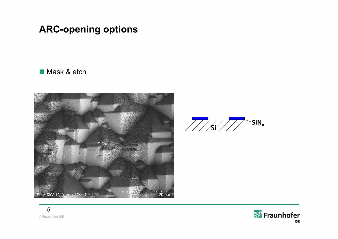
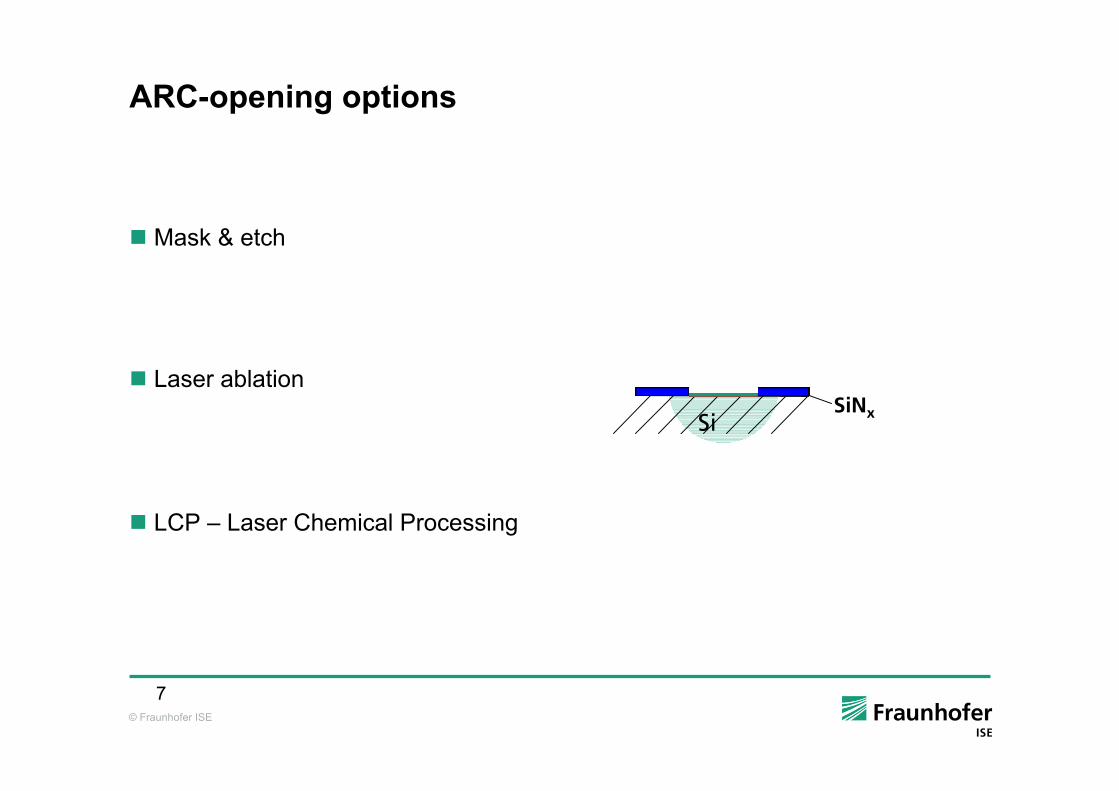
ARC-opening options
SiSiNx
Mask & etch
© Fraunhofer ISE
6
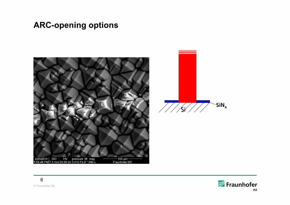
ARC-opening options
SiSiNx
Mask & etch
Laser ablation
© Fraunhofer ISE
7
ARC-opening options
SiSiNx
Mask & etch
Laser ablation
LCP – Laser Chemical Processing
© Fraunhofer ISE
8
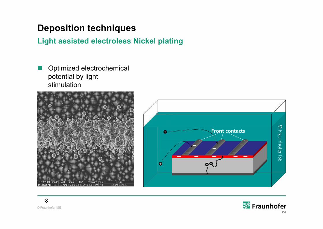
Deposition techniques
Optimized electrochemical potential by light stimulation
Light assisted electroless Nickel plating

© Fraunhofer ISE
9
Deposition techniques
Plating of Ni by electrochemical deposition
LIP - Light Induced Plating of nickel
© Fraunhofer ISE
10
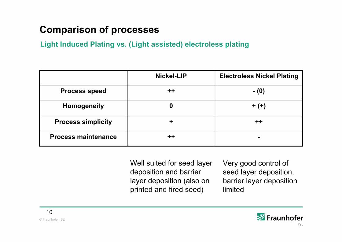
Comparison of processesLight Induced Plating vs. (Light assisted) electroless plating
+ (+)0Homogeneity
-++Process maintenance
+++Process simplicity
- (0)++Process speed
Electroless Nickel PlatingNickel-LIP
Well suited for seed layerdeposition and barrier layer deposition (also onprinted and fired seed)
Very good control ofseed layer deposition,barrier layer depositionlimited
© Fraunhofer ISE
11
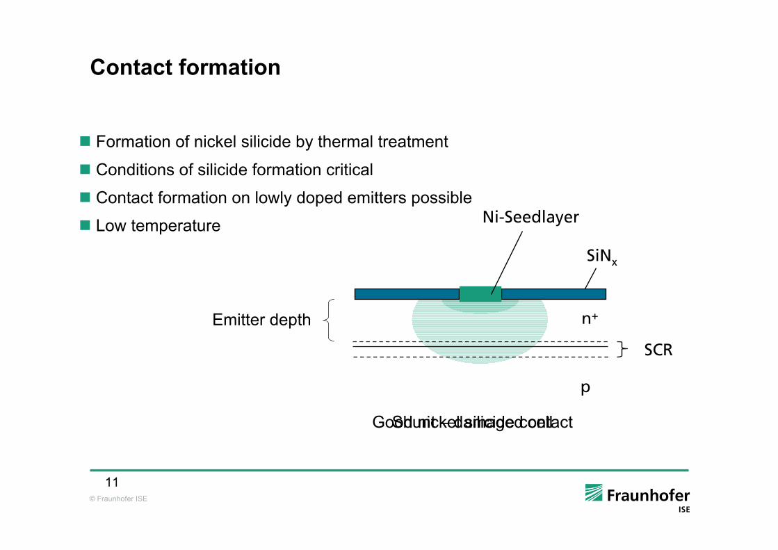
Contact formation
SCR
n+
p
SiNx
Ni Seedlayer
Formation of nickel silicide by thermal treatment
Good nickel silicide contactShunt – damaged cell
Conditions of silicide formation critical
Contact formation on lowly doped emitters possible
Low temperature
Emitter depth
© Fraunhofer ISE
12
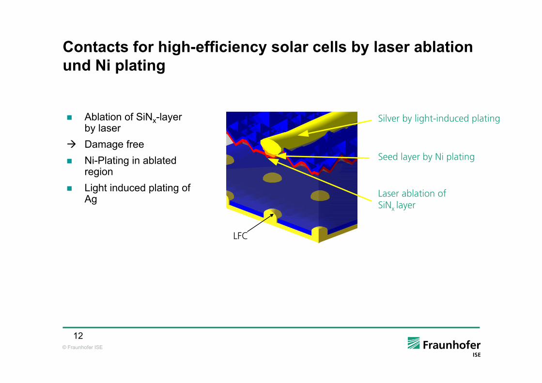
Contacts for high-efficiency solar cells by laser ablation und Ni plating
Ablation of SiNx-layer by laserDamage freeNi-Plating in ablated regionLight induced plating of Ag
Seed layer by Ni plating
Silver by light-induced plating
LFC
Laser ablation of SiNx layer

© Fraunhofer ISE
13
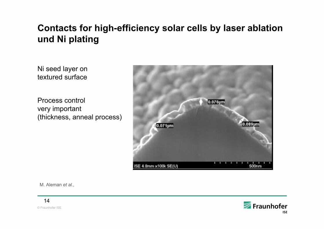
Contacts for high-efficiency solar cells by laser ablation und Ni plating
Ni seed layer ontextured surface
Process controlvery important(thickness, anneal process)
M. Aleman et al.,
© Fraunhofer ISE
14
Contacts for high-efficiency solar cells by laser ablation und Ni plating
Ni seed layer ontextured surface
Process controlvery important(thickness, anneal process)
M. Aleman et al.,
© Fraunhofer ISE
15
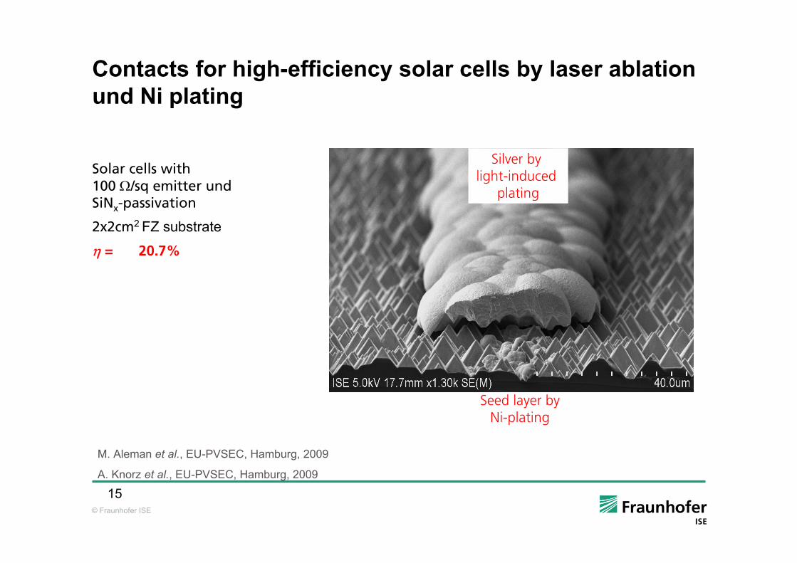
Contacts for high-efficiency solar cells by laser ablation und Ni plating
Solar cells with 100 Ω/sq emitter und SiNx passivation
2x2cm2 FZ substrate
η = 20.7%
Seed layer byNi-plating
Silver by light-induced
plating
M. Aleman et al., EU-PVSEC, Hamburg, 2009
A. Knorz et al., EU-PVSEC, Hamburg, 2009
© Fraunhofer ISE
16
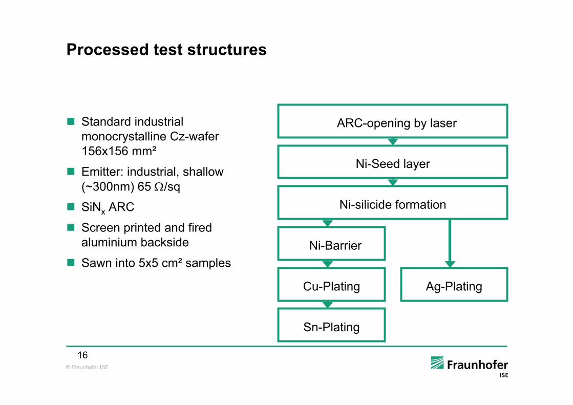
Processed test structures
Standard industrial monocrystalline Cz-wafer 156x156 mm²
Emitter: industrial, shallow (~300nm) 65 Ω/sqSiNx ARC
Screen printed and fired aluminium backside
Sawn into 5x5 cm² samples
ARC-opening by laser
Ni-Seed layer
Ni-Barrier
Cu-Plating Ag-Plating
Sn-Plating
Ni-silicide formation
© Fraunhofer ISE
17
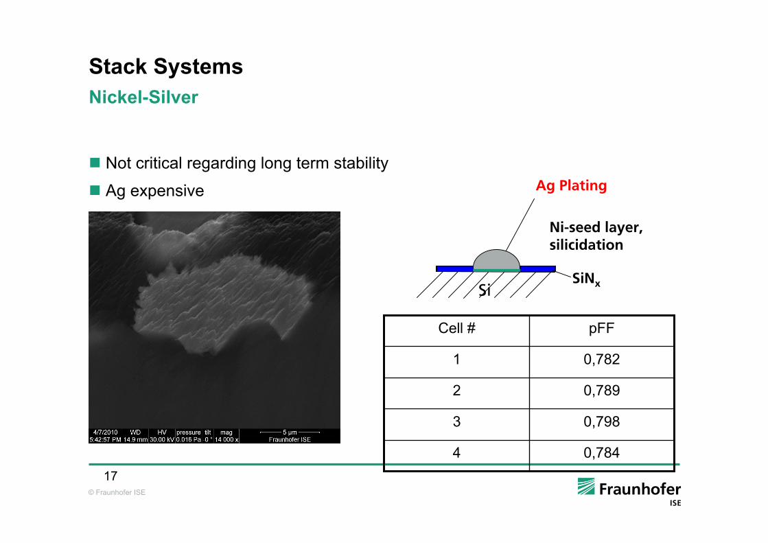
Stack Systems
Not critical regarding long term stability
Ag expensive Ag Plating
SiSiNx
Ni seed layer, silicidation
0,7844
0,7983
0,7892
0,7821
pFFCell #
Nickel-Silver
© Fraunhofer ISE
18
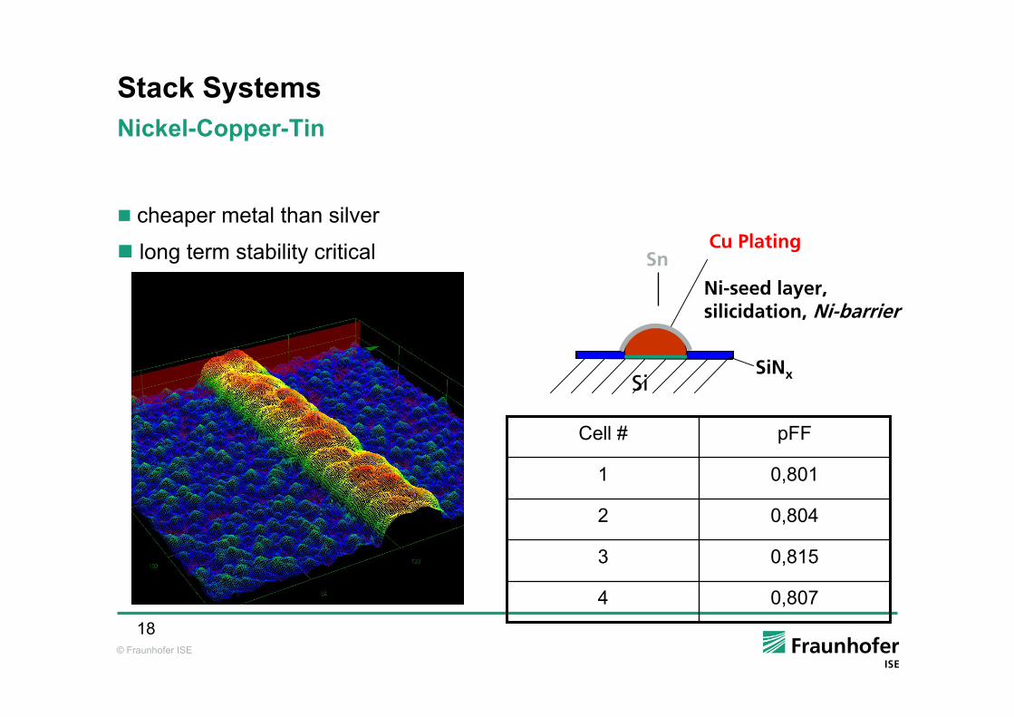
Cu Plating
Stack Systems
cheaper metal than silver
long term stability critical
SiSiNx
Ni seed layer, silicidation, Ni barrier
Sn
0,8074
0,8153
0,8042
0,8011
pFFCell #
Nickel-Copper-Tin
© Fraunhofer ISE
19
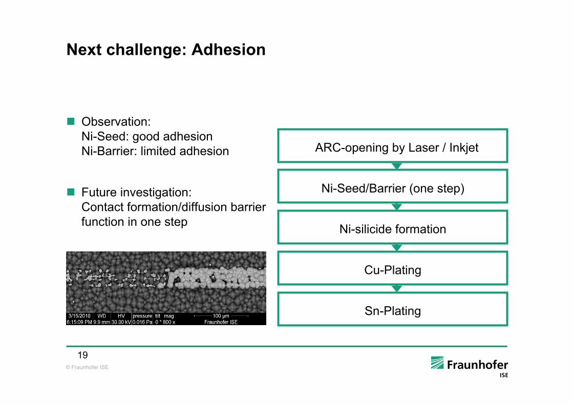
Next challenge: Adhesion
Observation: Ni-Seed: good adhesionNi-Barrier: limited adhesion
Future investigation:Contact formation/diffusion barrier function in one step
ARC-opening by Laser / Inkjet
Ni-Seed/Barrier (one step)
Cu-Plating
Sn-Plating
Ni-silicide formation

© Fraunhofer ISE
20
Durability
Problematic nature of Copper
Long term stability
First result: diffusion barrier function highly effectiveEstimation: 100h at 200°Ccorresponds to >100 years module lifetime
© Fraunhofer ISE
21
Conclusion
Nickel is suitable for contact formation due to its low contact resistance
Contact formation on shallow emitters could be achieved
Relatively simple method (self aligning, low temperature)
Possibility of the use of Copper
Adhesion problems to tackle
© Fraunhofer ISE
22
Thank You Very Much for Your Attention!
Andrew Mondon
Fraunhofer Institute for Solar Energy Systems ISE
© Fraunhofer ISE
23
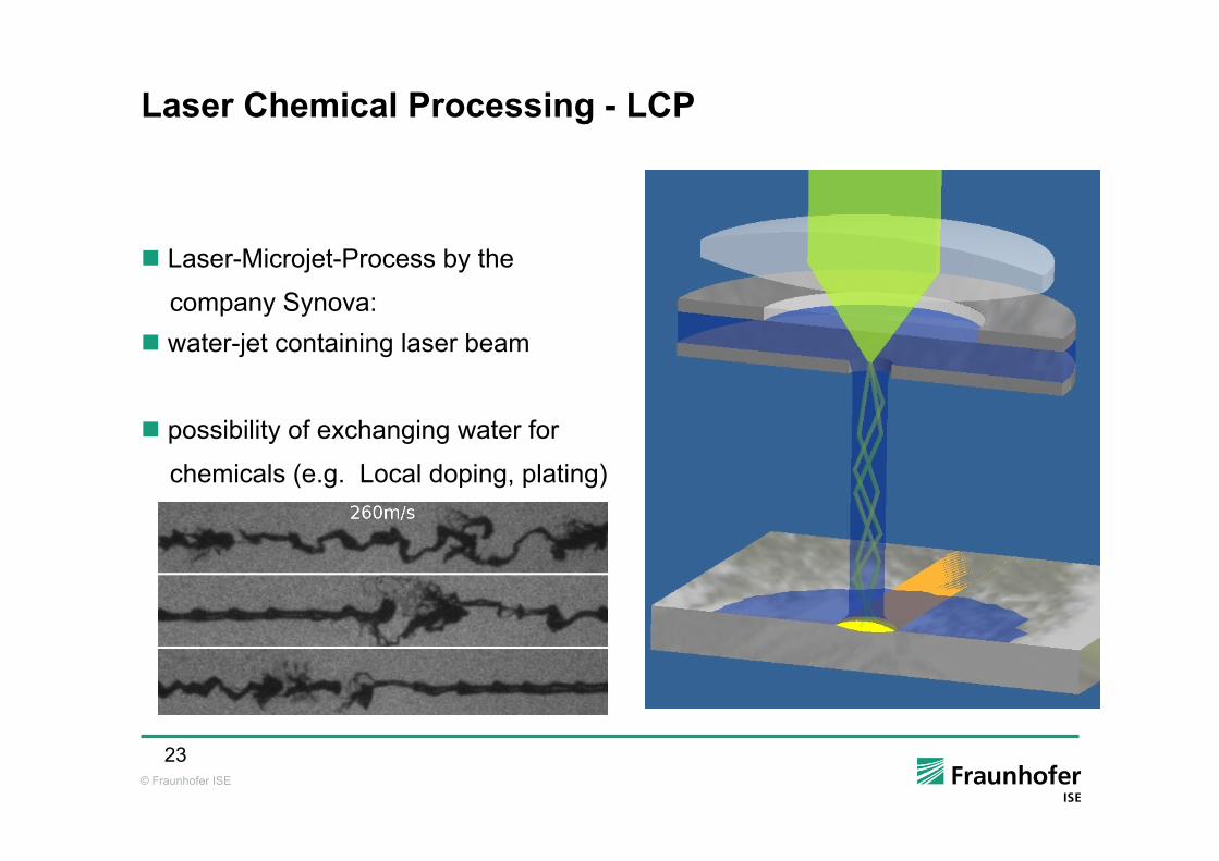
Laser Chemical Processing - LCP
Laser-Microjet-Process by the
company Synova:water-jet containing laser beam
possibility of exchanging water for
chemicals (e.g. Local doping, plating)