Low Voltage Low Power Dram Robert Mills Presentation for: High Speed and Low Power VLSI design...
25
Low Voltage Low Power Dram Robert Mills Presentation for: High Speed and Low Power VLSI design course Instructor: Prof. M. Shams
-
Upload
maximilian-holland -
Category
Documents
-
view
215 -
download
0
Transcript of Low Voltage Low Power Dram Robert Mills Presentation for: High Speed and Low Power VLSI design...
Low Voltage Low Power Dram
Low Voltage Low Power Dram
Robert MillsRobert Mills
Presentation for:High Speed and Low Power VLSI design course
Instructor: Prof. M. Shams
Presentation for:High Speed and Low Power VLSI design course
Instructor: Prof. M. Shams

IntroductionIntroduction
Rapidly growing area of Power Aware systemsDRAM Design EvolutionGoal: Identify Power Sources in Drams Present Design SolutionsExamine Ultra Low Power issues (Future
Concerns) Proposed Project Plan and Schedule
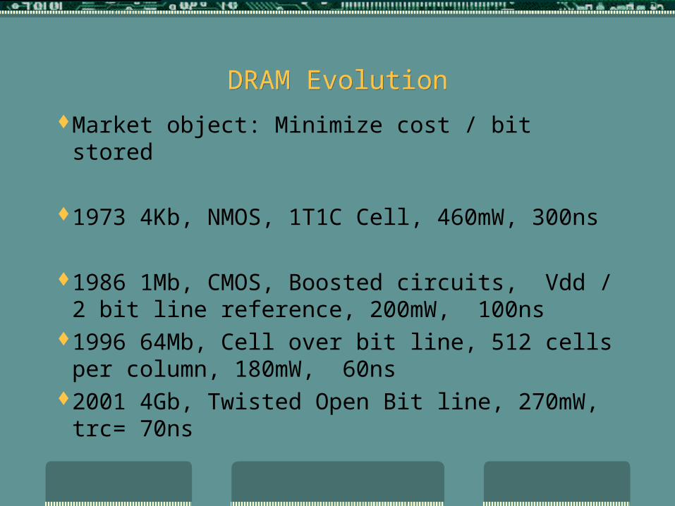
DRAM EvolutionDRAM Evolution
Market object: Minimize cost / bit stored
1973 4Kb, NMOS, 1T1C Cell, 460mW, 300ns
1986 1Mb, CMOS, Boosted circuits, Vdd / 2 bit line reference, 200mW, 100ns
1996 64Mb, Cell over bit line, 512 cells per column, 180mW, 60ns
2001 4Gb, Twisted Open Bit line, 270mW, trc= 70ns
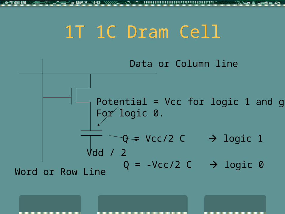
1T 1C Dram Cell1T 1C Dram Cell
Word or Row Line
Data or Column line
Vdd / 2
Potential = Vcc for logic 1 and gnd For logic 0.
Q = Vcc/2 C logic 1
Q = -Vcc/2 C logic 0
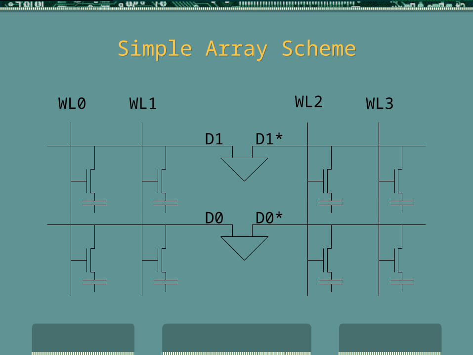
Simple Array SchemeSimple Array Scheme
WL0 WL1 WL2 WL3
D0 D0*
D1 D1*
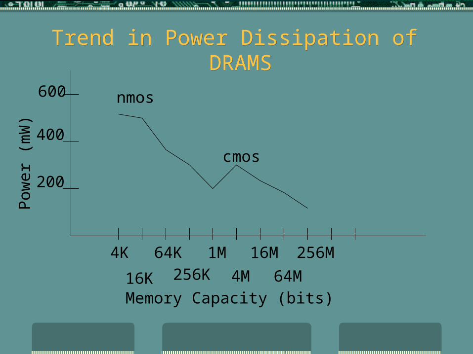
Trend in Power Dissipation of DRAMS
Trend in Power Dissipation of DRAMS
4K
16K
64K
256K
1M
64M4M
16M 256M
200
400
600 nmos
cmos
Pow
er (
mW
)
Memory Capacity (bits)
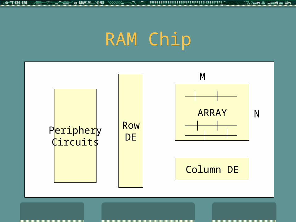
RAM ChipRAM Chip
ARRAY
Column DE
RowDE
PeripheryCircuits
M
N
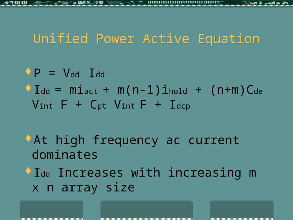
Unified Power Active EquationUnified Power Active Equation
P = Vdd Idd
Idd = miact + m(n-1)ihold + (n+m)Cde Vint F + Cpt Vint F + Idcp
At high frequency ac current dominatesIdd Increases with increasing m x n array size
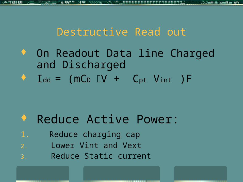
Destructive Read outDestructive Read out
On Readout Data line Charged and Discharged
Idd = (mCD V + Cpt Vint )F
Reduce Active Power:1. Reduce charging cap2. Lower Vint and Vext3. Reduce Static current
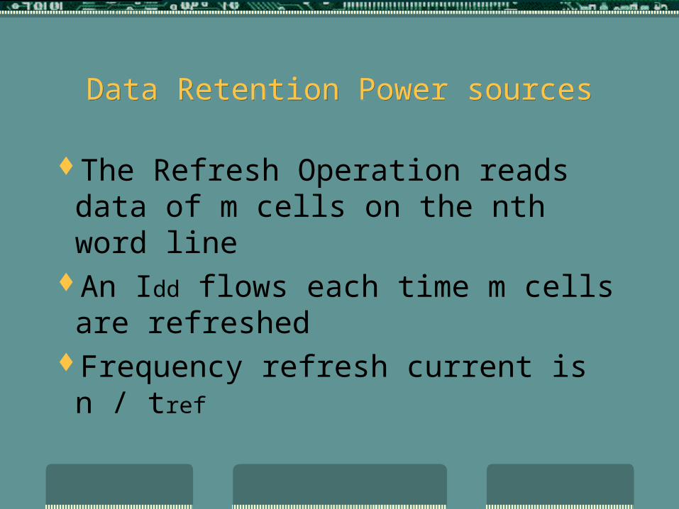
Data Retention Power sourcesData Retention Power sources
The Refresh Operation reads data of m cells on the nth word line
An Idd flows each time m cells are refreshedFrequency refresh current is n / tref

Low Power Dram CircuitsLow Power Dram Circuits
Charge Capacitance Reduction by partial activation of Multi-divided data line.
Increase in memory cells directly increases the CD
Divide one data line into several sections & activate only one sub-section.
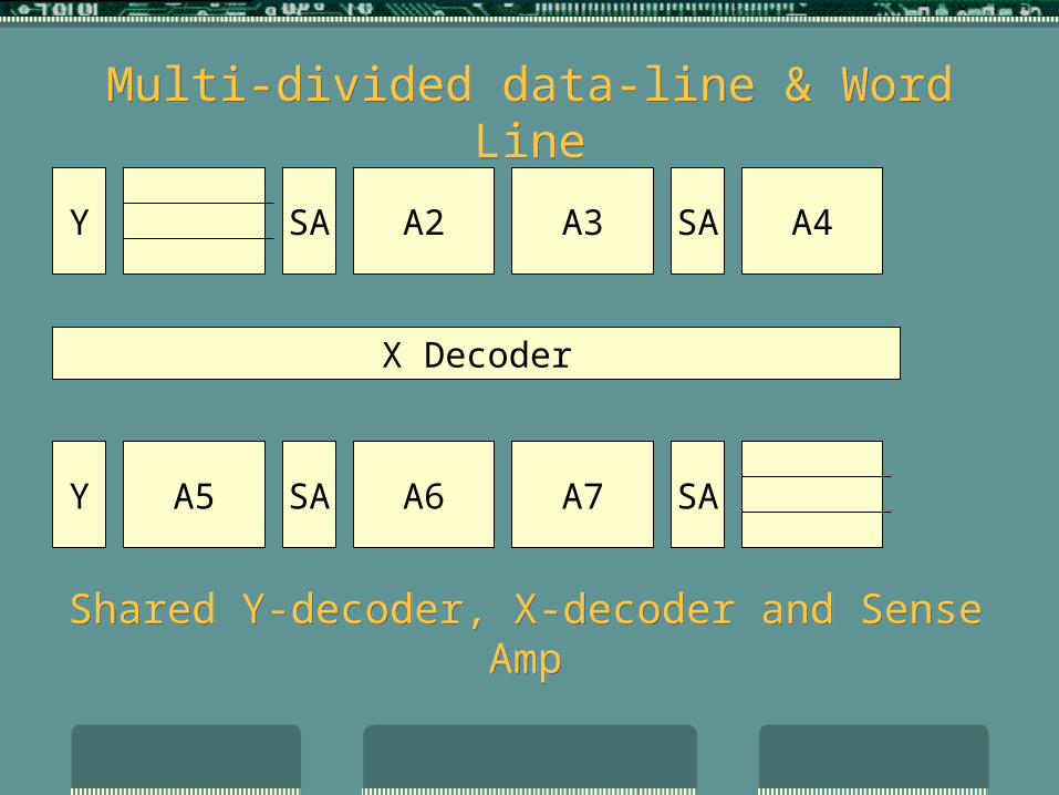
Multi-divided data-line & Word LineMulti-divided data-line & Word Line
Y SA
X Decoder
A2 SAA3 A4
Y A5 SA A6 SAA7
Shared Y-decoder, X-decoder and Sense Amp
Shared Y-decoder, X-decoder and Sense Amp
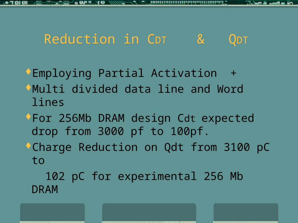
Reduction in CDT & QDT Reduction in CDT & QDT
Employing Partial Activation +Multi divided data line and Word linesFor 256Mb DRAM design Cdt expected drop
from 3000 pf to 100pf.Charge Reduction on Qdt from 3100 pC to 102 pC for experimental 256 Mb DRAM
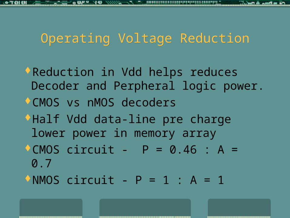
Operating Voltage ReductionOperating Voltage Reduction
Reduction in Vdd helps reduces Decoder and Perpheral logic power.
CMOS vs nMOS decoders Half Vdd data-line pre charge lower power in
memory arrayCMOS circuit - P = 0.46 : A = 0.7 NMOS circuit - P = 1 : A = 1
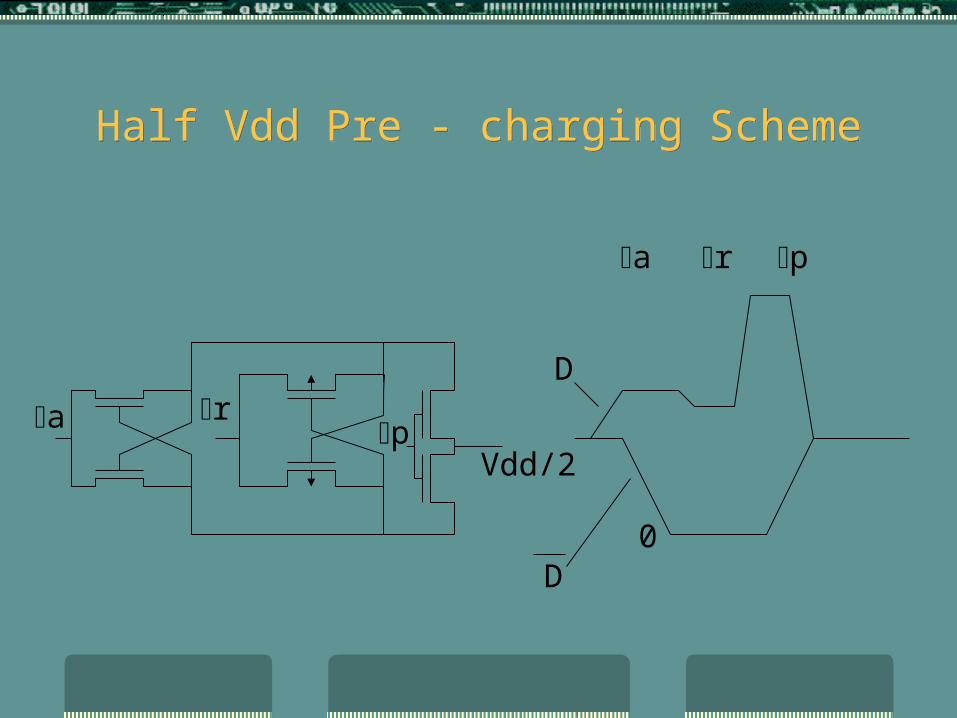
Half Vdd Pre - charging SchemeHalf Vdd Pre - charging Scheme
pVdd/2
r
0
D
D
a r p
a
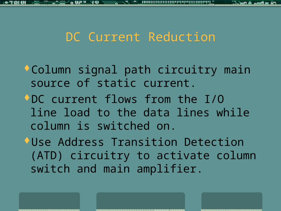
DC Current ReductionDC Current Reduction
Column signal path circuitry main source of static current.
DC current flows from the I/O line load to the data lines while column is switched on.
Use Address Transition Detection (ATD) circuitry to activate column switch and main amplifier.
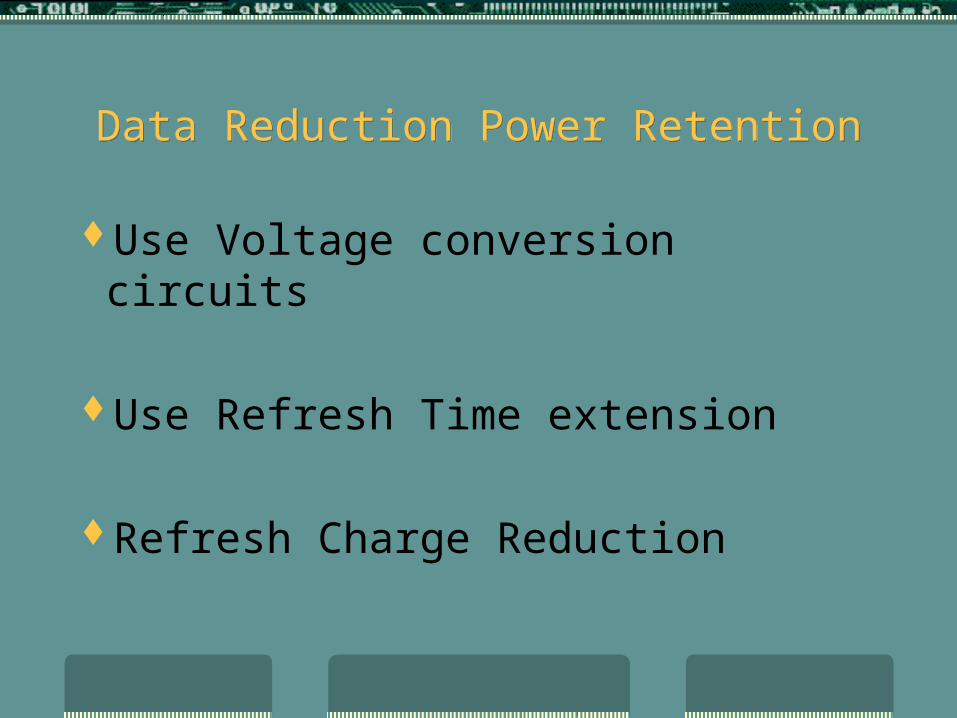
Data Reduction Power RetentionData Reduction Power Retention
Use Voltage conversion circuits
Use Refresh Time extension
Refresh Charge Reduction
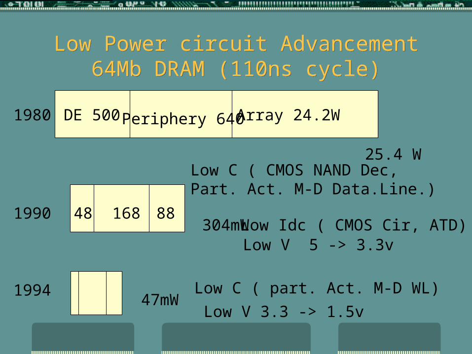
Low Power circuit Advancement64Mb DRAM (110ns cycle)
Low Power circuit Advancement64Mb DRAM (110ns cycle)
1980
25.4 W
DE 500 Periphery 640 Array 24.2W
199447mW
Low V 3.3 -> 1.5v
Low C ( part. Act. M-D WL)
1990304mW
48 168 88Low Idc ( CMOS Cir, ATD)
Low C ( CMOS NAND Dec, Part. Act. M-D Data.Line.)
Low V 5 -> 3.3v
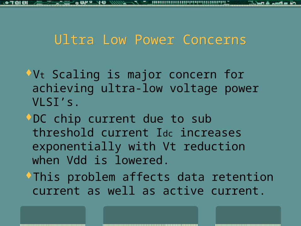
Ultra Low Power ConcernsUltra Low Power Concerns
Vt Scaling is major concern for achieving ultra-low voltage power VLSI’s.
DC chip current due to sub threshold current Idc increases exponentially with Vt reduction when Vdd is lowered.
This problem affects data retention current as well as active current.
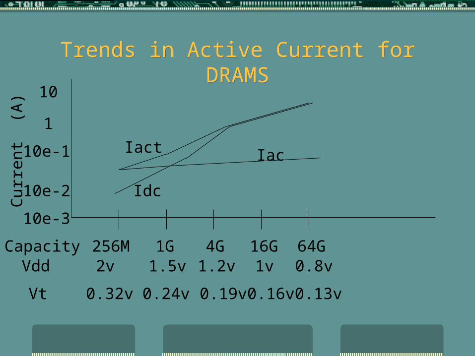
Trends in Active Current for DRAMSTrends in Active Current for DRAMS
Capacity 256M 1G 4G 16G 64G
10e-1
10e-3
10e-2
10
1
Cur
rent
(A
)
IacIact
Idc
Vdd
Vt
2v 1.5v 1.2v 1v 0.8v
0.32v 0.24v 0.19v 0.16v 0.13v
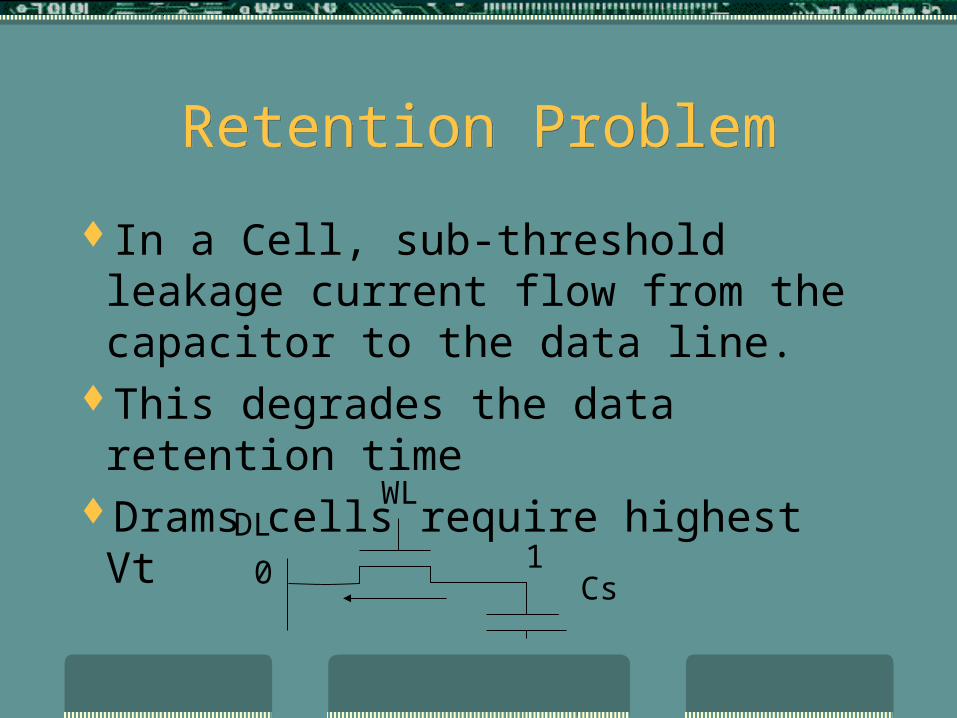
Retention ProblemRetention Problem
In a Cell, sub-threshold leakage current flow from the capacitor to the data line.
This degrades the data retention timeDrams cells require highest Vt
WLDL
Cs10
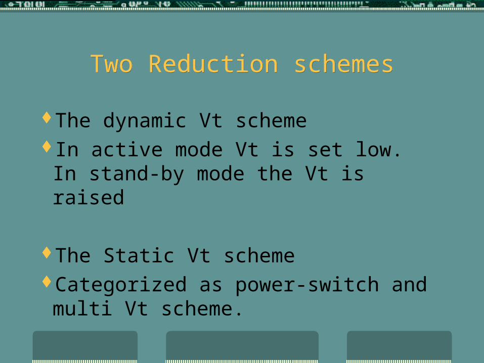
Two Reduction schemesTwo Reduction schemes
The dynamic Vt schemeIn active mode Vt is set low. In stand-by mode
the Vt is raised
The Static Vt schemeCategorized as power-switch and multi Vt
scheme.
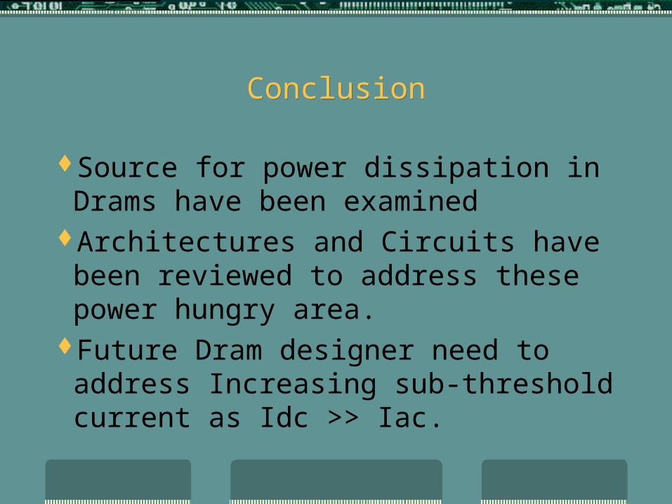
ConclusionConclusion
Source for power dissipation in Drams have been examined
Architectures and Circuits have been reviewed to address these power hungry area.
Future Dram designer need to address Increasing sub-threshold current as Idc >> Iac.

Project Plan & ScheduleProject Plan & Schedule
Design an Address Decoder and Optimize for low power DRAM application.
Define design problem: 1st – 7th AprilOptimize & design Decoder: 8 -15th AprilSimulate both designs: 16-22th AprilPresent Results week of 23rd AprilSubmit in report on 5th May
ReferencesReferences
“Fast Low Power Decoders for Rams”, M. Horowitz, IEEE JSSC, Vol,36, No.10, Oct 2001
“Low Voltage Memories for Power-Aware Systems”,Itoh, ISLPED ’02, August 12-14, 2002, Monterey, California, USA.
“A 4Gb DDR SDRAM with Gain controlled Pre-Sensing and Ref. Bitline Calibration Schemes in the twisted Open Bitline Architecture”, H. Yoon et al., IEEE, ISSCC-2001 Session 24/DRAM/24.1, Feb. 2001
“Limitations and Challenges of Multigigabit DRAM Chip Design”, Itoh, IEEE JSSC, Vol. 32, No. 5, May 1997.
“Trends in Low Power RAM Circuit Technologies”, Itoh et al, Proceedings of the
IEEE, Vol. 83, No.4 April 1995.