Low-loss polysilicon waveguides fabricated in an … · Low-loss polysilicon waveguides fabricated...
12
Low-loss polysilicon waveguides fabricated in an emulated high-volume electronics process Jason S. Orcutt, 1* Sanh D. Tang, 2 Steve Kramer, 2 Karan Mehta, 1 Hanqing Li, 1 Vladimir Stojanović, 1 and Rajeev J. Ram 1 1 Massachusetts Institute of Technology, 77 Massachusetts Ave, Cambridge, Massachusetts 02139, USA 2 Micron Technology, Inc., 8000 South Federal Way, Post Office Box 6, Boise, Idaho 83707, USA *[email protected] Abstract: We measure end-of-line polysilicon waveguide propagation losses of ~6-15 dB/cm across the telecommunication O-, E-, S-, C- and L- bands in a process representative of high-volume product integration. The lowest loss of 6.2 dB/cm is measured at 1550 nm in a polysilicon waveguide with a 120 nm x 350 nm core geometry. The reported waveguide characteristics are measured after the thermal cycling of the full CMOS electronics process that results in a 32% increase in the extracted material loss relative to the as-crystallized waveguide samples. The measured loss spectra are fit to an absorption model using defect state parameters to identify the dominant loss mechanism in the end-of-line and as-crystallized polysilicon waveguides. ©2012 Optical Society of America OCIS Codes: (230.7370) Waveguides; (250.5300) Photonic integrated circuits; (220.4000) Microstructure fabrication. References and links 1. M. J. Kobrinski, B. A. Block, J.-F. Zheng, B. C. Barnett, E. Mohammed, M. Reshotko, F. Robertson, S. List, I. Young, and K. Cadien, “On-chip optical interconnects,” Intel Technol. J. 8, 129–141 (2004). 2. D. A. B. Miller, “Device requirements for optical interconnects to silicon chips,” Proc. IEEE 97(7), 1166–1185 (2009). 3. S. Beamer, C. Sun, Y.-J. Kwon, A. Joshi, C. Batten, V. Stojanović, and K. Asanović, “Re-architecting DRAM memory systems with monolithically integrated silicon photonics,” in International Symposium on Computer Architecture (Association for Computing Machinery, New York 2010), 129–140. 4. P. Dumon, W. Bogaerts, V. Wiaux, J. Wouters, S. Beckx, J. Van Campenhout, D. Taillaert, B. Luyssaert, P. Bienstman, D. Van Thourhout, and R. Baets, “Low-loss SOI photonic wires and ring resonators fabricated with deep UV lithography,” IEEE Photon. Technol. Lett. 16(5), 1328–1330 (2004). 5. C. Gunn, “CMOS photonics for high-speed interconnects,” IEEE Micro 26(2), 58–66 (2006). 6. X. Zheng, J. Lexau, Y. Luo, H. Thacker, T. Pinguet, A. Mekis, G. Li, J. Shi, P. Amberg, N. Pinckney, K. Raj, R. Ho, J. E. Cunningham, and A. V. Krishnamoorthy, “Ultra-low-energy all-CMOS modulator integrated with driver,” Opt. Express 18(3), 3059–3070 (2010), http://www.opticsinfobase.org/oe/abstract.cfm?URI=oe-18-3- 3059. 7. Y. Vlasov, W. M. J. Green, and F. Xia, “High-throughput silicon nanophotonic wavelength-insensitive switch for on-chip optical networks,” Nat. Photonics 2(4), 242–246 (2008). 8. T. Ohsawa, K. Fujita, K. Hatsuda, T. Higashi, M. Morikado, Y. Minami, T. Shino, H. Nakajima, K. Inoh, T. Hamamoto, and S. Watanabe, “An 18.5ns 128MB SOI DRAM with floating body cell,” in International Solid- State Circuits Conference (Institute of Electrical and Electronics Engineers, New York, 2005), 459–609. 9. J. A. Kash, “Leveraging optical interconnects in future supercomputers and servers,” in Proc. IEEE Symposium on High-Performance Interconnects (Institute of Electrical and Electronics Engineers, New York 2008), 190– 194. 10. A. M. Agarwal, L. Liao, J. S. Foresi, M. R. Black, X. Duan, and L. C. Kimerling, “Low-loss polycrystalline silicon waveguides for silicon photonics,” J. Appl. Phys. 80(11), 6120–6123 (1996). 11. K. Preston, S. Manipatruni, A. Gondarenko, C. B. Poitras, and M. Lipson, “Deposited silicon high-speed integrated electro-optic modulator,” Opt. Express 17(7), 5118–5124 (2009), http://www.opticsinfobase.org/abstract.cfm?URI=oe-17-7-5118. 12. I. A. Young, E. Mohammed, J. T. S. Liao, A. M. Kern, S. Palermo, B. A. Block, M. R. Reshotko, and P. L. D. Chang, “Optical I/O technology for tera-scale computing,” IEEE J. Solid-state Circuits 45(1), 235–248 (2010). #162227 - $15.00 USD Received 30 Jan 2012; revised 7 Mar 2012; accepted 12 Mar 2012; published 14 Mar 2012 (C) 2012 OSA 26 March 2012 / Vol. 20, No. 7 / OPTICS EXPRESS 7243
Transcript of Low-loss polysilicon waveguides fabricated in an … · Low-loss polysilicon waveguides fabricated...

Low-loss polysilicon waveguides fabricated in an
emulated high-volume electronics process
Jason S. Orcutt,1*
Sanh D. Tang,2 Steve Kramer,
2 Karan Mehta,
1 Hanqing Li,
1 Vladimir
Stojanović,1 and Rajeev J. Ram
1
1Massachusetts Institute of Technology, 77 Massachusetts Ave, Cambridge, Massachusetts 02139, USA 2Micron Technology, Inc., 8000 South Federal Way, Post Office Box 6, Boise, Idaho 83707, USA
Abstract: We measure end-of-line polysilicon waveguide propagation
losses of ~6-15 dB/cm across the telecommunication O-, E-, S-, C- and L-
bands in a process representative of high-volume product integration. The
lowest loss of 6.2 dB/cm is measured at 1550 nm in a polysilicon
waveguide with a 120 nm x 350 nm core geometry. The reported waveguide
characteristics are measured after the thermal cycling of the full CMOS
electronics process that results in a 32% increase in the extracted material
loss relative to the as-crystallized waveguide samples. The measured loss
spectra are fit to an absorption model using defect state parameters to
identify the dominant loss mechanism in the end-of-line and as-crystallized
polysilicon waveguides.
©2012 Optical Society of America
OCIS Codes: (230.7370) Waveguides; (250.5300) Photonic integrated circuits; (220.4000)
Microstructure fabrication.
References and links
1. M. J. Kobrinski, B. A. Block, J.-F. Zheng, B. C. Barnett, E. Mohammed, M. Reshotko, F. Robertson, S. List, I.
Young, and K. Cadien, “On-chip optical interconnects,” Intel Technol. J. 8, 129–141 (2004).
2. D. A. B. Miller, “Device requirements for optical interconnects to silicon chips,” Proc. IEEE 97(7), 1166–1185
(2009).
3. S. Beamer, C. Sun, Y.-J. Kwon, A. Joshi, C. Batten, V. Stojanović, and K. Asanović, “Re-architecting DRAM
memory systems with monolithically integrated silicon photonics,” in International Symposium on Computer
Architecture (Association for Computing Machinery, New York 2010), 129–140.
4. P. Dumon, W. Bogaerts, V. Wiaux, J. Wouters, S. Beckx, J. Van Campenhout, D. Taillaert, B. Luyssaert, P.
Bienstman, D. Van Thourhout, and R. Baets, “Low-loss SOI photonic wires and ring resonators fabricated with
deep UV lithography,” IEEE Photon. Technol. Lett. 16(5), 1328–1330 (2004).
5. C. Gunn, “CMOS photonics for high-speed interconnects,” IEEE Micro 26(2), 58–66 (2006).
6. X. Zheng, J. Lexau, Y. Luo, H. Thacker, T. Pinguet, A. Mekis, G. Li, J. Shi, P. Amberg, N. Pinckney, K. Raj, R.
Ho, J. E. Cunningham, and A. V. Krishnamoorthy, “Ultra-low-energy all-CMOS modulator integrated with
driver,” Opt. Express 18(3), 3059–3070 (2010), http://www.opticsinfobase.org/oe/abstract.cfm?URI=oe-18-3-
3059.
7. Y. Vlasov, W. M. J. Green, and F. Xia, “High-throughput silicon nanophotonic wavelength-insensitive switch for
on-chip optical networks,” Nat. Photonics 2(4), 242–246 (2008).
8. T. Ohsawa, K. Fujita, K. Hatsuda, T. Higashi, M. Morikado, Y. Minami, T. Shino, H. Nakajima, K. Inoh, T.
Hamamoto, and S. Watanabe, “An 18.5ns 128MB SOI DRAM with floating body cell,” in International Solid-
State Circuits Conference (Institute of Electrical and Electronics Engineers, New York, 2005), 459–609.
9. J. A. Kash, “Leveraging optical interconnects in future supercomputers and servers,” in Proc. IEEE Symposium
on High-Performance Interconnects (Institute of Electrical and Electronics Engineers, New York 2008), 190–
194.
10. A. M. Agarwal, L. Liao, J. S. Foresi, M. R. Black, X. Duan, and L. C. Kimerling, “Low-loss polycrystalline
silicon waveguides for silicon photonics,” J. Appl. Phys. 80(11), 6120–6123 (1996).
11. K. Preston, S. Manipatruni, A. Gondarenko, C. B. Poitras, and M. Lipson, “Deposited silicon high-speed
integrated electro-optic modulator,” Opt. Express 17(7), 5118–5124 (2009),
http://www.opticsinfobase.org/abstract.cfm?URI=oe-17-7-5118.
12. I. A. Young, E. Mohammed, J. T. S. Liao, A. M. Kern, S. Palermo, B. A. Block, M. R. Reshotko, and P. L. D.
Chang, “Optical I/O technology for tera-scale computing,” IEEE J. Solid-state Circuits 45(1), 235–248 (2010).
#162227 - $15.00 USD Received 30 Jan 2012; revised 7 Mar 2012; accepted 12 Mar 2012; published 14 Mar 2012(C) 2012 OSA 26 March 2012 / Vol. 20, No. 7 / OPTICS EXPRESS 7243

13. S. Kalluri, M. Ziari, A. Chen, V. Chuyanov, W. H. Steier, D. Chen, B. Jalali, H. Fetterman, and L. R. Dalton,
“Monolithic integration of waveguide polymer electrooptic modulators on VLSI circuitry,” IEEE Photon.
Technol. Lett. 8(5), 644–646 (1996).
14. B. A. Block, T. R. Younkin, P. S. Davids, M. R. Reshotko, P. Chang, B. M. Polishak, S. Huang, J. Luo, and A.
K. Y. Jen, “Electro-optic polymer cladding ring resonator modulators,” Opt. Express 16(22), 18326–18333
(2008), http://www.opticsinfobase.org/abstract.cfm?URI=oe-16-22-18326.
15. G. Masini, L. Colace, and G. Assanto, “2.5 Gbit/s polycrystalline germanium-on-silicon photodetector operating
from 1.3 to 1.55 µm,” Appl. Phys. Lett. 82(15), 2524–2526 (2003).
16. S. Assefa, F. Xia, and Y. A. Vlasov, “Reinventing germanium avalanche photodetector for nanophotonic on-chip
optical interconnects,” Nature 464(7285), 80–84 (2010).
17. J. S. Orcutt, A. Khilo, C. W. Holzwarth, M. A. Popović, H. Li, J. Sun, T. Bonifield, R. Hollingsworth, F. X.
Kärtner, H. I. Smith, V. Stojanović, and R. J. Ram, “Nanophotonic integration in state-of-the-art CMOS
foundries,” Opt. Express 19(3), 2335–2346 (2011), http://www.opticsinfobase.org/abstract.cfm?URI=oe-19-3-
2335.
18. H.-C. Ji, K. H. Ha, I. S. Joe, S. G. Kim, K. W. Na, D. J. Shin, S. D. Suh, Y. D. Park, and C. H. Chung, “Optical
interface platform for DRAM integration,” in Optical Fiber Communication Conference, OSA Technical Digest
(CD) (Optical Society of America, 2011), paper OThV4.
http://www.opticsinfobase.org/abstract.cfm?URI=OFC-2011-OThV4
19. J. S. Orcutt, S. D. Tang, S. Kramer, H. Li, V. Stojanović, and R. J. Ram, “Low-loss polysilicon waveguides
suitable for integration within a high-volume electronics process,” in Conference on Lasers and Electro-Optics,
Technical Digest (CD) (Optical Society of America, 2011), paper CThHH2.
http://www.opticsinfobase.org/abstract.cfm?URI=CLEO: S and I-2011-CThHH2
20. J. S. Foresi, M. R. Black, A. M. Agarwal, and L. C. Kimerling, “Losses in polycrystalline silicon waveguides,”
Appl. Phys. Lett. 68(15), 2052–2054 (1996).
21. Q. Fang, J. F. Song, S. H. Tao, M. B. Yu, G. Q. Lo, and D. L. Kwong, “Low loss (~6.45 dB/cm) sub-micron
polycrystalline silicon waveguide integrated with efficient SiON waveguide coupler,” Opt. Express 16, 6425–
6432. http://www.opticsinfobase.org/abstract.cfm?URI=oe-16-9-6425
22. L. Liao, D. R. Lim, A. M. Agarwal, X. Duan, K. K. Lee, and L. C. Kimerling, “Optical transmission losses in
polycrystalline silicon strip waveguides: effects of waveguide dimensions, thermal treatment, hydrogen
passivation, and wavelength,” J. Electron. Mater. 29(12), 1380–1386 (2000).
23. S. Zhu, Q. Fang, M. B. Yu, G. Q. Lo, and D. L. Kwong, “Propagation losses in undoped and n-doped
polycrystalline silicon wire waveguides,” Opt. Express 17(23), 20891–20899 (2009),
http://www.opticsinfobase.org/abstract.cfm?URI=oe-17-23-20891.
24. S. Zhu, G. Q. Lo, J. D. Ye, and D. L. Kwong, “Influence of RTA and LTA on the optical propagation loss in
polycrystalline silicon wire waveguides,” IEEE Photon. Technol. Lett. 22(7), 480–482 (2010).
25. C. W. Holzwarth, J. S. Orcutt, H. Li, M. A. Popović, V. Stojanović, J. L. Hoyt, R. J. Ram, and H. I. Smith,
“Localized substrate removal technique enabling strong-confinement microphotonics in bulk Si CMOS
processes,” in Conference on Lasers and Electro-Optics, Technical Digest (CD) (Optical Society of America,
2008), paper CThKK5. http://www.opticsinfobase.org/abstract.cfm?URI=CLEO-2008-CThKK5
26. T. Barwicz and H. A. Haus, “Three-dimensional analysis of scattering losses due to sidewall roughness in
microphotonic waveguides,” IEEE J. Lightwave Technol. 23(9), 2719–2732 (2005).
27. S. Sridaran and S. A. Bhave, “Nanophotonic devices on thin buried oxide Silicon-On-Insulator substrates,” Opt.
Express 18(4), 3850–3857 (2010), http://www.opticsinfobase.org/abstract.cfm?URI=oe-18-4-3850.
28. J. E. Cunningham, I. Shubin, X. Zheng, T. Pinguet, A. Mekis, Y. Luo, H. Thacker, G. Li, J. Yao, K. Raj, and A.
V. Krishnamoorthy, “Highly-efficient thermally-tuned resonant optical filters,” Opt. Express 18(18), 19055–
19063 (2010), http://www.opticsinfobase.org/abstract.cfm?URI=oe-18-18-19055.
29. http://www.research.ibm.com/DAMOCLES/html_files/phys.html
30. W. B. Jackson, N. M. Johnson, and D. K. Biegelsen, “Density of gap states of silicon grain boundaries
determined by optical absorption,” Appl. Phys. Lett. 43(2), 195–197 (1983).
1. Introduction
Integration of silicon photonic devices alongside traditional silicon electronics has been a
continuing research effort to provide high bandwidth-density communication channels with
lower energy requirements than electronic links [1–3]. Although thick-buried-oxide (BOX),
silicon-on-insulator (SOI) wafers have become the dominant monolithic silicon photonic
platform due to the easy formation of low-loss waveguides [4–7], the majority of VLSI
applications (e.g. microprocessors, systems-on-chip (SOCs) and field-programmable gate
arrays (FPGAs)) and manufacturers require the use of bulk-silicon wafers instead (for cost
and performance reasons – e.g. thermal impact of thick BOX). For high-volume, high-density
memory products such as DRAM, bulk-silicon wafers also remain the dominant production
platform. SOI-based memory processes have failed to gain widespread acceptance due to the
higher wafer cost and existing bulk manufacturing base [8]. To enable the silicon photonic
#162227 - $15.00 USD Received 30 Jan 2012; revised 7 Mar 2012; accepted 12 Mar 2012; published 14 Mar 2012(C) 2012 OSA 26 March 2012 / Vol. 20, No. 7 / OPTICS EXPRESS 7244

system application of replacing the existing chip-to-chip core-to-memory electrical links of a
computer system with integrated photonic links, photonic devices must be intimately
integrated with the DRAM and CMOS microprocessor chips [3]. As such, further
development of integrated photonic platforms that utilize bulk-silicon wafers is required.
It is possible to avoid substrate incompatibility between the dominant silicon photonic and
electronic platforms by adopting a non-monolithic layer stacking approach. Low-parasitic
through silicon via (TSV) interconnection and bonding strategies enable a separately
fabricated SOI photonic layer to be integrated with the existing bulk-silicon electronic die as
part of a 3D platform [6, 9]. Indeed, memory vendors are already exploring bonding multiple
memory die to increase storage density per package. Although this may prove to be a valuable
approach, there are several limitations. For a given 3D layer count, a photonic access layer
would reduce the storage capacity of the end product by occupying an available stack layer.
Also, the energy budget of the total optical interconnect link must be expanded to include the
parasitic-limited electrical interlayer communication as well as decrease in energy-efficiency
of optical link backend circuits resulting from poorer transistor performance in thick-BOX
SOI processes.
Instead of relying on a separate photonic layer, several past research efforts have proposed
monolithically adding photonic devices into the backend stackup of a CMOS process where
the starting substrate does not affect functionality [10–13]. Significant technical progress has
been made to fabricate photonic devices under the unique low-temperature and complex
topography conditions of the electronic backend process in recent years [14, 15]. However,
backend photonic integration would add new mask steps and wafer processing to the
electronic manufacturing process. This constraint is particularly severe for DRAM
manufacturing. The cost sensitivity and yield constraints of the memory market limit the
number of process steps and masks to the absolute minimums required. Steps that cannot be
shared with existing electronic processing represent significant overall cost burdens.
To provide photonic integration with minimum impact to the overall system, front-end
integration with a deposited high-index core layer is required. By integrating the photonic
layer into the front-end process, all following process steps that are used to form the
transistors can be leveraged to form the active and passive photonic devices. These existing
steps include high-resolution lithography, low edge-roughness etching, multiple doping
implants, activation annealing, silicidation, high-aspect ratio contact vias and many levels of
low parasitic metal interconnect. Given this vast toolset, many active and passive photonic
elements can be integrated with no increase in fabrication cost and complexity. The high
thermal budget of this point of the process flow also allows for the integration of high quality
photodetectors as demonstrated in recent work [16]. To maximally leverage the available
processing steps, the photonic integration point studied in this work is to utilize the
polysilicon transistor gate layer as the waveguide core. All contact and most implant process
steps occur after the deposition of this layer. Additionally, the existing photolithography used
for this layer is among the highest resolution patterning steps available within the existing
electronics process. The polysilicon waveguide layer is separated from the underlying bulk-
silicon wafer substrate by the oxide trench isolation used to electrically isolate transistors. The
backend metal and dielectric interconnect stackup is then fabricated on top of the polysilicon
waveguides.
We have previously demonstrated an example of such a platform in a bulk-CMOS process
[17]. However, the mask-share, generic process model of the CMOS foundry under study in
past work prevented process optimization and has limited the end-of-line polysilicon
waveguide loss to ~55 dB/cm at 1550nm. In this work, we study an optimized polysilicon
deposition and crystallization process to reduce the end-of-line waveguide loss. Although this
platform is equally applicable to future bulk-CMOS processes, the focus of this study will be
a DRAM fabrication process. DRAM products couple the process and mask design such that
high-volume manufacturing processes are optimized to the specific memory product under
#162227 - $15.00 USD Received 30 Jan 2012; revised 7 Mar 2012; accepted 12 Mar 2012; published 14 Mar 2012(C) 2012 OSA 26 March 2012 / Vol. 20, No. 7 / OPTICS EXPRESS 7245
production. The process flow of the overall DRAM product may then be optimized to include
photonic-specific modifications to achieve system goals while minimizing cost and
complexity. It also opens new avenues for stacked DRAM development and further
improvements in communication efficiency, by enabling photonics within the stack and in
each DRAM stack-layer [3].
Recently, reports of solid phase epitaxy (SPE) silicon waveguides [18] and polysilicon
waveguides [19] have demonstrated 6.1 dB/cm and 6.2 dB/cm propagation losses respectively
in DRAM integrable platforms. The recently-proposed single-crystalline SPE silicon platform
requires the deposition and recrystallization of an additional front-end layer to serve as a
waveguide core. In addition to the cost of the additional layer, the yield of the fabricated
devices may be coupled to the heterogeneous crystallization regions formed during SPE [18].
Although this approach may prove to be a valuable integration platform, we instead optimize
the existing polysilicon layer present in the process as the transistor gate for use as an
alternate low-optical loss waveguide core. Here, we further report on the polysilicon
waveguide platform that enables a high-yield, low-loss photonic platform within high-volume
memory products with minimal increases in fabrication cost and complexity. The fabrication
flow in a 300 mm wafer facility was designed to emulate high-volume memory integration by
including the thermal cycling and full dielectric stack-up of an existing production process.
To provide a viable photonic platform for most system applications, low polysilicon
waveguide loss must be demonstrated at end-of-line in the integrated electronic platform.
Significant academic work has reduced polysilicon waveguide losses from initial reports of
100-300 dB/cm [20] to the lowest demonstrated loss of 6.5 dB/cm [21] accompanied by
several reports of waveguide loss below 20 dB/cm [10, 11, 22–25]. However, no
demonstration of propagation loss below 10 dB/cm has been achieved for a polysilicon layer
thickness below 200 nm to be compatible with scaled transistor gate thicknesses or in a
process representative of electronic integration. These two differences have been
demonstrated to have a large impact on waveguide loss in previous studies. In Fang et al., the
loss nearly doubled from 7.1 dB/cm to 14 dB/cm when the thickness of the polysilicon layer
was reduced from 250 nm to 150 nm for the same 500 nm core width. The previous front-end
integration work in bulk-CMOS processes demonstrated the impact of the thermal processing
and the local dielectric environment of the electronics process. Significant loss increase was
observed between as-crystallized polysilicon waveguides with ~10 dB/cm loss [25] and the
end-of-line integrated waveguide losses of 55 dB/cm [17].
In this work, we demonstrate end-of-line 6.2 dB/cm loss at 1550 nm for a single-mode
polysilicon waveguide with a 120 nm layer thickness in an electronics integration emulation
process representative of a state-of-the-art DRAM product on 300 mm wafers. The emulation
flow was chosen instead of the full fabrication flow to reduce cost, but all thermal cycling and
wafer-level processes to produce the surrounding dielectric environment are performed to
match the existing product. Since the wavelength band of operation for an integrated system is
not constrained to 1550 nm, we measure waveguide propagation losses across the
telecommunication O-, E-, S-, C- and L-bands (1260 nm to 1630 nm). Although the extracted
bulk material absorption ranges from 4.4 cm−1
to 7.8 cm−1
, confinement factor scaling enables
single-mode waveguide propagation losses below 15 dB/cm across this wavelength range. By
comparing the 120 nm polysilicon thickness waveguides to similarly prepared samples with a
200 nm polysilicon thickness, we estimate that despite a low top surface roughness of 0.3 nm
RMS, the top surface roughness may account for up to 10% of the wide waveguide loss. To
isolate the effect of the thermal processing, we compare waveguide loss from the full
electronics emulation process to an as-crystallized wafer split to show that the thermal
processing causes ~25% of the end-of-line polysilicon material loss. By then fitting the
extracted material losses to a polysilicon absorption model based on grain-boundary defect
state parameters from the literature, defect state absorption from the polysilicon is shown to
be the dominant loss mechanism in both the as-crystallized and thermally processed
#162227 - $15.00 USD Received 30 Jan 2012; revised 7 Mar 2012; accepted 12 Mar 2012; published 14 Mar 2012(C) 2012 OSA 26 March 2012 / Vol. 20, No. 7 / OPTICS EXPRESS 7246
polysilicon samples. Only transverse-electric (TE) modes are considered in this work due to
the high asymmetry of the thin-core waveguides.
2. Process overview
Leveraging previous extensive studies of polysilicon loss as a function of deposition and
anneal conditions [22, 24], we selected an amorphous polysilicon deposition condition used
for a transistor gate in an existing product and inserted a post-deposition anneal into the
process flow to control grain formation. This deposition condition, similar to what has been
used in previous polysilicon waveguide studies, differs from the more widely used transistor
gate deposition conditions that typically occur above the roughly ~600 °C threshold for
silicon crystal nucleation. In these higher temperature depositions, the crystals that form
during growth form a columnar grain structure that produces a top surface roughness on the
order of 5 nm RMS [17]. The theoretical loss prediction that would result from such a
roughness is ~50 dB/cm for the TE mode of 400 nm wide, 120 nm thick polysilicon
waveguide assuming a 50 nm correlation length to the roughness [26]. Utilizing low-pressure
chemical vapor deposition (LPCVD) below the crystallization temperature, a smooth top
surface of 0.3 nm RMS was achieved as measured by in-line atomic force microscopy (AFM).
Prior to normal electronic thermal processing that would crystallize the amorphous film under
an arbitrary condition, a ~950 °C, 20 s anneal was performed in an inert N2 atmosphere. The
insertion of this anneal step after the polysilicon deposition has no impact on the electronic
device performance due to the high thermal budget of the early front-end process. The
polysilicon deposition and anneal occurs immediately after the well implant diffusion which
involves a >1000 °C anneal for over an hour.
All wafer-level processing was performed in a commercial fabrication facility on 300 mm
bulk silicon wafers. The polysilicon was deposited on a 200-300 nm oxide to match the
shallow trench isolation used in the memory process. After deposition and anneal of 120 nm
and 200 nm thick polysilicon films on different wafers, standard 193 nm photolithography
and reactive ion etching (RIE) was performed to form the waveguides. Next, the wafers were
split between those that would and would not be exposed to the full memory process thermal
cycling. After thermal cycling was performed on a subset of the wafers, all wafers reported
here were clad with the complete, multi-layer dielectric stack-up as is used in the existing
memory product. Although all dielectric layers that are within 1 µm of the polysilicon have a
refractive index similar to that of fused silica, the heterogeneous electronic stack-up includes
higher index layers such as silicon carbide that function as etch stops in the standard process.
Since the shallow trench isolation that formed the waveguide lower cladding was not
sufficiently thick to isolate the optical mode from the substrate, die-level substrate removal
was performed in an academic cleanroom for this study. This step may be obviated in an end
product by increasing the thickness of the shallow trench isolation or the insertion of a deep
trench isolation specifically for this purpose [18] to provide optical mode isolation. However,
since these changes involve significant re-engineering of the front-end process, an alternative
approach that would be suitable for an end system is localized substrate removal [17, 25, 27,
28]. In this work, blanket substrate removal was performed to minimize sample preparation
complexity. To do this, the diced sample was mounted substrate-up on a 6-inch, oxidized
#162227 - $15.00 USD Received 30 Jan 2012; revised 7 Mar 2012; accepted 12 Mar 2012; published 14 Mar 2012(C) 2012 OSA 26 March 2012 / Vol. 20, No. 7 / OPTICS EXPRESS 7247
Fig. 1. (a) Cartoon cross-section of the memory process used for this work. All unlabeled
dielectric layers in the immediate proximity of the waveguide core have a refractive index
close to that of fused silica at the wavelengths of interest. (b) Waveguide mode profile contours
for a narrow waveguide at 1550 nm with 120 nm polysilicon layer thickness illustrating the
asymmetry introduced by the substrate removal and low polysilicon guided power fraction. (c)
High-confinement waveguide modes such as that of an 800 nm waveguide width show no
observable asymmetry and clearly confine the majority of the light in the polysilicon core
region.
silicon wafer for thermal management using Crystalbond 509. The silicon substrate was then
removed by using XeF2 in a pulse-etch process. Etch cycles of 10 s interleaved by 50 s pump
cycles to remove reaction products were repeated until the substrate was removed as
monitored under an optical microscope. The high selectivity of silicon to oxide of the XeF2
etchant enables cm-scale die to be processed without consuming a measureable fraction of the
shallow trench isolation etch stop. The final cross section and resulting waveguide modes are
shown in Fig. 1. The substrate removal process results in an asymmetric waveguide mode due
to the refractive index asymmetry as shown in Fig. 1(b).
3. Test platform and measurement results
A set of test structures was designed to characterize the waveguide loss for each fabrication
condition as a function of waveguide width and wavelength. The basic test cell is built from
“paperclip” structures where different lengths of straight waveguides are connected by
identical bends and coupling structures. Single-mode bends connect through 25 µm tapers to
the straight test section of various waveguide widths to ensure that the transmission of the
fundamental mode is measured. These tapered regions of equal length can be seen in Fig.
2(b). Two sets of four total test section lengths are included for each test waveguide width and
measurement wavelength range. The low loss test set comprised of three bend paperclips has
total test section lengths of 60 µm, 3.3 mm, 6.9 mm, 10.5 mm. The high loss test set
comprised of single bend paperclips has total test section lengths of 20 µm, 0.9 mm, 2.4 mm,
3.9 mm. An example micrograph of two such test cells is shown in Fig. 2(a). The differential
transmission within a set of paperclips can then be related to the propagation loss as in the
cutback method. Transmission measurements can only be compared within the set of high
#162227 - $15.00 USD Received 30 Jan 2012; revised 7 Mar 2012; accepted 12 Mar 2012; published 14 Mar 2012(C) 2012 OSA 26 March 2012 / Vol. 20, No. 7 / OPTICS EXPRESS 7248

Fig. 2. (a) Optical micrograph of “paperclip” waveguide loss test structures for three
waveguide widths. Four differential lengths each are used to measure propagation losses in two
sets designed for high and low loss cases. (b) The width of the straight section is varied by
introducing tapers between single-mode waveguide bends to ensure that the transmission of
only the fundamental mode is measured. Single-mode lead widths of 376 nm, 476 nm and 600
nm are used for 1.25 µm, 1.4 µm and 1.55 µm wavelength centers respectively. The chosen
bend radius of 15 µm reduces the total excess bending loss of the lead waveguides to below 1
dB. (c) Uniform grating couplers with 200 µm long linear tapers are designed for 10.5 µm
input mode diameter for an 8° off-normal incident angle. Design grating periods 819 nm, 974
nm and 1067 nm with duty cycles 37.5%, 37.5% and 42.5% are used for 1.25 µm, 1.4 µm and
1.55 µm wavelength centers respectively.
loss or low loss paperclip lengths such that the number of lead waveguide bends and total lead
waveguide length are kept constant for each test structure. As a result, the total insertion loss
associated with the couplers, lead waveguides, tapers and bends is kept constant for each
measurement involved in a given calculation such that the differential loss between
measurements is only affected by the propagation loss in the straight waveguide test sections
under study. The mask includes waveguide loss test cells for 13 different waveguide widths
between 200 nm and 2 µm repeated for wavelength centers of 1550 nm, 1400 nm and 1250
nm. Broadband grating couplers with 150 nm bandwidth below 10 dB insertion loss are
shown in Fig. 2(c). Conservative single-mode bend sizing for the lead waveguides then
enables testing over the continuous wavelength spectrum from 1150 nm to 1650 nm.
Due to the limited availability of laser sources for this testing, reported results are
restricted to the range of 1280 nm to 1630 nm. Input and output fiber coupling to the
fabricated vertical coupler gratings occurs from the “back-side” of the sample where the
silicon substrate has been removed during post-foundry processing. The “front-side” of the
sample is mounted to the handle oxidized silicon wafer for structural support. Since the
degeneracy between upwards and downwards radiation is not broken in the grating coupler
design, the insertion loss is approximately equal for coupling from either side. Cleaved single-
mode fibers with a mode field diameter (MFD) of 10.4 µm at 1550 nm wavelength are used
for this coupling at an angle 8 degrees off from normal incidence. Input fiber TE polarization
to the grating couplers is set through a paddle-based controller by minimizing the insertion
loss in short waveguide test structures where the total transmission loss is dominated by the
coupler insertion loss. Since the vertical grating coupler insertion loss at this incidence angle
for the TM mode is greater than 30 dB per coupler, high input polarization selectivity is
possible. Device-under-test (DUT) transmission loss is then measured by comparing received
output power to a 10% power tap directional coupler output that is present in the input fiber
path. Although only relative transmission loss measurements are used for the propagation loss
calculations, the absolute transmission loss of the setup is calibrated as a function of
#162227 - $15.00 USD Received 30 Jan 2012; revised 7 Mar 2012; accepted 12 Mar 2012; published 14 Mar 2012(C) 2012 OSA 26 March 2012 / Vol. 20, No. 7 / OPTICS EXPRESS 7249

wavelength by replacing the DUT input and output fibers with a 1 meter fiber patch cord and
recording the output fiber and tap fiber received powers. For all of the measurements reported
in this work, the optical power of the input fiber was maintained to be approximately 1 mW.
The losses of the various test cells, shown in Fig. 3, were then measured for wafers with a
120 nm polysilicon thickness after the thermal cycling representative of the full electronics
process. Several trends emerge from the data. First, reduced waveguide widths enable
confinement factor scaling to reduce the contribution of the propagation loss from the
polysilicon material as illustrated in Fig. 1(b). Measured propagation loss scales with
decreasing confinement factor down to approximately 30%. This enables measured
waveguide losses below 15 dB/cm across the telecommunications spectrum despite
significantly higher waveguide loss at wider waveguide widths. A waveguide width of 350
nm enables the lowest reported propagation loss of 6.2 dB/cm for a thin-core polysilicon
waveguide at 1550 nm.
The second trend is the abrupt end to the loss reduction through confinement factor
scaling achieved by narrowing the waveguide width for each wavelength. If this were to be
attributed to sidewall scattering having a larger impact on propagation loss, a more gradual
transition to increased loss would be expected [26]. Additionally, mode solving simulations
verify that the effective indices of the fundamental modes of these high loss widths are above
that of any dielectric layers bordering the polysilicon core such that the waveguide is not close
to cutoff. There is, however, a thin, high-index silicon carbide layer that is part of the backend
electronic stack-up as an etch stop layer as shown in Fig. 1(a). The effective indices of the
slab waveguide modes of this layer fall in between the effective indices of the low loss and
high loss waveguide widths for each wavelength as shown in Fig. 4(b). Although the SiC
layer is ~2 µm away from the waveguide core, mode solving simulations show significant
electric field overlap with the SiC layer, shown in Fig. 1(a), at the widths where the sudden
loss increase is observed. Therefore phase-matched coupling between the dielectric etch stop
layers and the waveguide mode may set the limit to confinement factor scaling of waveguide
loss when integrated in similar electronic platforms.
Fig. 3. Measured propagation loss as a function of wavelength and waveguide width for a
thermally processed wafer with a 120 nm polysilicon thickness. The error bars of the
measurements are calculated from the 95% confidence intervals of the transmission loss as
function of paperclip test section length measurements. Cross-wafer and wafer-to-wafer
variability data was not taken. Measurements of different die from the reported wafers agreed
within the precision of the propagation loss fit error bars reported. Simulation curves for the
confinement factor scaling of waveguide bulk loss were then fit to the measured loss of the
wide waveguides and are shown alongside the measured data for comparison.
#162227 - $15.00 USD Received 30 Jan 2012; revised 7 Mar 2012; accepted 12 Mar 2012; published 14 Mar 2012(C) 2012 OSA 26 March 2012 / Vol. 20, No. 7 / OPTICS EXPRESS 7250

Fig. 4. Simulated waveguide mode (a) confinement factor and (b) effective index. Confinement
factor curves from (a) are multiplied by the extracted bulk loss to generate the fit curves shown
in Fig. 3. Effective index curves are overlaid with the simulated 1D slab mode index for the
SiC layer that is correlated with the observed loss increase across measured wavelengths.
A final trend visible from the data shown in Fig. 3 is a consistent increase in waveguide
propagation loss at shorter wavelengths for wide waveguides. Since the majority of the optical
power is guided in the polysilicon core region at these widths, this increase can be attributed
to the bulk material loss scaling with wavelength. The approximate bulk material loss of the
polysilicon can then be extracted by dividing the measured propagation loss of the wide
waveguides by the simulated confinement factors. This data is then shown in Fig. 5(a) for a
larger number of wavelengths by dividing the measured propagation loss by the simulated
confinement factors for 1.5 µm and 2.0 µm waveguide widths shown in Fig. 4(a). This same
analysis was also performed for wafers prepared identically to the data presented in Fig. 3
with the exception that the thermal cycling associated with the full electronics process was not
performed. Comparing the two data sets, a 32% increase in the extracted material loss is
observed as shown in Fig. 5(c) with a standard deviation of 6% across the wavelength range
studied. Importantly, this increase is far below the order of magnitude increase that has been
observed in previous work [17, 25].
To gain some insight into the source of the waveguide loss, the extracted wavelength-
dependent bulk losses were compared to theoretical predictions. The material loss was
calculated by accounting for electronic transitions between mid-gap states localized at grain
boundaries and Bloch states in the conduction and valence bands. Assuming a constant
average oscillator strength for all involved transitions between band and midgap states, the
absorption coefficient calculated from Fermi’s Golden Rule can be written as a function of the
valence, conduction and midgap densities of states (DOS):
( ) ( ) ( ) ( )
( ) ( ) ( ) ( )
( ) 1
1
v v v g v v v
g g g c g g g
A dE E E f E f E
dE E E f E f E
α ω ρ ρ ω ω
ρ ρ ω ω
= + − +
+ + − +
∫
∫
ℏ ℏ
ℏ ℏ
The two integrals sum transitions from the valence band states (DOSvρ ) to the midgap
states (DOS g
ρ ), and from the midgap states to the conduction band (DOS cρ ), as
diagrammed in Fig. 5(b). The Fermi distribution function, f, enforces that all considered
transitions occur between filled initial and empty final states, separated by the photon energy.
Unlike the valence and conduction band density of states, the midgap state density parameter
represents only a functional form of the midgap state energy distribution, which is chosen to
#162227 - $15.00 USD Received 30 Jan 2012; revised 7 Mar 2012; accepted 12 Mar 2012; published 14 Mar 2012(C) 2012 OSA 26 March 2012 / Vol. 20, No. 7 / OPTICS EXPRESS 7251
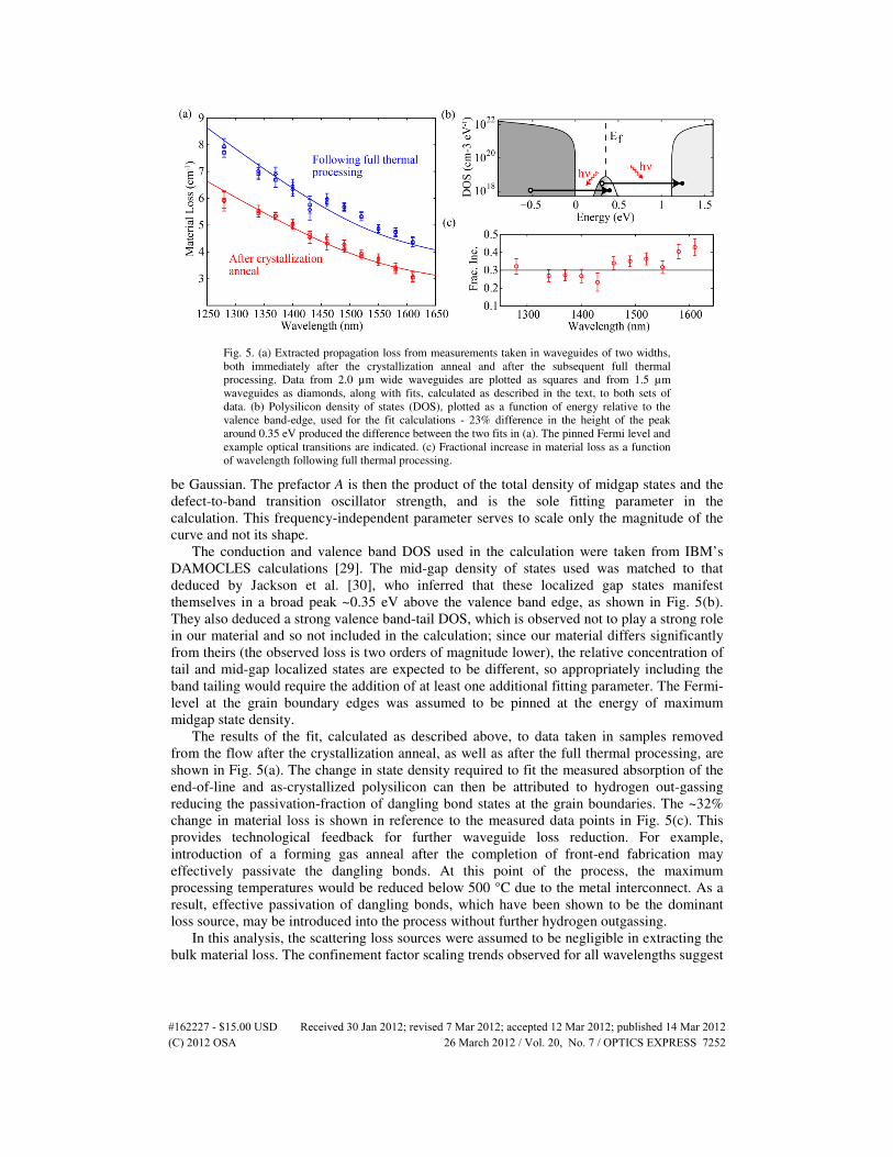
Fig. 5. (a) Extracted propagation loss from measurements taken in waveguides of two widths,
both immediately after the crystallization anneal and after the subsequent full thermal
processing. Data from 2.0 µm wide waveguides are plotted as squares and from 1.5 µm
waveguides as diamonds, along with fits, calculated as described in the text, to both sets of
data. (b) Polysilicon density of states (DOS), plotted as a function of energy relative to the
valence band-edge, used for the fit calculations - 23% difference in the height of the peak
around 0.35 eV produced the difference between the two fits in (a). The pinned Fermi level and
example optical transitions are indicated. (c) Fractional increase in material loss as a function
of wavelength following full thermal processing.
be Gaussian. The prefactor A is then the product of the total density of midgap states and the
defect-to-band transition oscillator strength, and is the sole fitting parameter in the
calculation. This frequency-independent parameter serves to scale only the magnitude of the
curve and not its shape.
The conduction and valence band DOS used in the calculation were taken from IBM’s
DAMOCLES calculations [29]. The mid-gap density of states used was matched to that
deduced by Jackson et al. [30], who inferred that these localized gap states manifest
themselves in a broad peak ~0.35 eV above the valence band edge, as shown in Fig. 5(b).
They also deduced a strong valence band-tail DOS, which is observed not to play a strong role
in our material and so not included in the calculation; since our material differs significantly
from theirs (the observed loss is two orders of magnitude lower), the relative concentration of
tail and mid-gap localized states are expected to be different, so appropriately including the
band tailing would require the addition of at least one additional fitting parameter. The Fermi-
level at the grain boundary edges was assumed to be pinned at the energy of maximum
midgap state density.
The results of the fit, calculated as described above, to data taken in samples removed
from the flow after the crystallization anneal, as well as after the full thermal processing, are
shown in Fig. 5(a). The change in state density required to fit the measured absorption of the
end-of-line and as-crystallized polysilicon can then be attributed to hydrogen out-gassing
reducing the passivation-fraction of dangling bond states at the grain boundaries. The ~32%
change in material loss is shown in reference to the measured data points in Fig. 5(c). This
provides technological feedback for further waveguide loss reduction. For example,
introduction of a forming gas anneal after the completion of front-end fabrication may
effectively passivate the dangling bonds. At this point of the process, the maximum
processing temperatures would be reduced below 500 °C due to the metal interconnect. As a
result, effective passivation of dangling bonds, which have been shown to be the dominant
loss source, may be introduced into the process without further hydrogen outgassing.
In this analysis, the scattering loss sources were assumed to be negligible in extracting the
bulk material loss. The confinement factor scaling trends observed for all wavelengths suggest
#162227 - $15.00 USD Received 30 Jan 2012; revised 7 Mar 2012; accepted 12 Mar 2012; published 14 Mar 2012(C) 2012 OSA 26 March 2012 / Vol. 20, No. 7 / OPTICS EXPRESS 7252
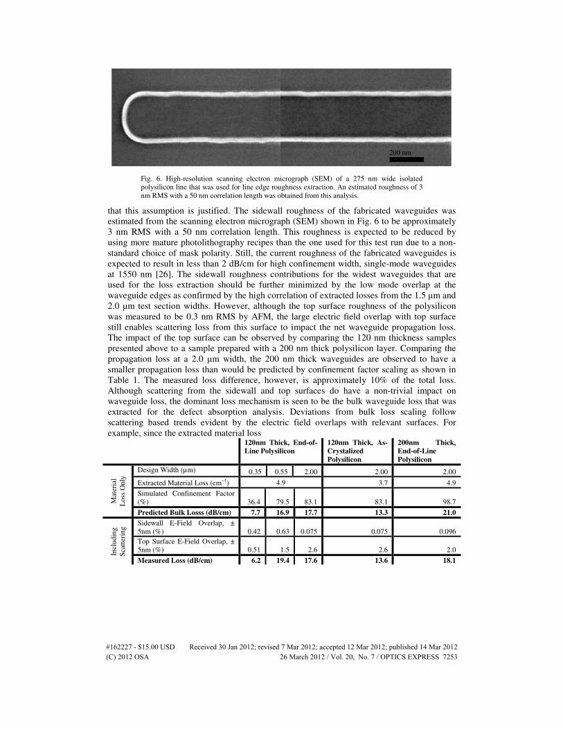
Fig. 6. High-resolution scanning electron micrograph (SEM) of a 275 nm wide isolated
polysilicon line that was used for line edge roughness extraction. An estimated roughness of 3
nm RMS with a 50 nm correlation length was obtained from this analysis.
that this assumption is justified. The sidewall roughness of the fabricated waveguides was
estimated from the scanning electron micrograph (SEM) shown in Fig. 6 to be approximately
3 nm RMS with a 50 nm correlation length. This roughness is expected to be reduced by
using more mature photolithography recipes than the one used for this test run due to a non-
standard choice of mask polarity. Still, the current roughness of the fabricated waveguides is
expected to result in less than 2 dB/cm for high confinement width, single-mode waveguides
at 1550 nm [26]. The sidewall roughness contributions for the widest waveguides that are
used for the loss extraction should be further minimized by the low mode overlap at the
waveguide edges as confirmed by the high correlation of extracted losses from the 1.5 µm and
2.0 µm test section widths. However, although the top surface roughness of the polysilicon
was measured to be 0.3 nm RMS by AFM, the large electric field overlap with top surface
still enables scattering loss from this surface to impact the net waveguide propagation loss.
The impact of the top surface can be observed by comparing the 120 nm thickness samples
presented above to a sample prepared with a 200 nm thick polysilicon layer. Comparing the
propagation loss at a 2.0 µm width, the 200 nm thick waveguides are observed to have a
smaller propagation loss than would be predicted by confinement factor scaling as shown in
Table 1. The measured loss difference, however, is approximately 10% of the total loss.
Although scattering from the sidewall and top surfaces do have a non-trivial impact on
waveguide loss, the dominant loss mechanism is seen to be the bulk waveguide loss that was
extracted for the defect absorption analysis. Deviations from bulk loss scaling follow
scattering based trends evident by the electric field overlaps with relevant surfaces. For
example, since the extracted material loss
120nm Thick, End-of-
Line Polysilicon
120nm Thick, As-
Crystalized
Polysilicon
200nm Thick,
End-of-Line
Polysilicon
Mat
eria
l
Lo
ss O
nly
Design Width (µm) 0.35 0.55 2.00 2.00 2.00
Extracted Material Loss (cm−1) 4.9 3.7 4.9
Simulated Confinement Factor
(%) 36.4 79.5 83.1 83.1 98.7
Predicted Bulk Losss (dB/cm) 7.7 16.9 17.7 13.3 21.0
Incl
ud
ing
Sca
tter
ing Sidewall E-Field Overlap, ±
5nm (%) 0.42 0.63 0.075 0.075 0.096
Top Surface E-Field Overlap, ±
5nm (%) 0.51 1.5 2.6 2.6 2.0
Measured Loss (dB/cm) 6.2 19.4 17.6 13.6 18.1
#162227 - $15.00 USD Received 30 Jan 2012; revised 7 Mar 2012; accepted 12 Mar 2012; published 14 Mar 2012(C) 2012 OSA 26 March 2012 / Vol. 20, No. 7 / OPTICS EXPRESS 7253

Table 1. Summary of experimentally measured waveguide losses, bulk absorption
calculations and electric field overlaps with surfaces where roughness is a concern.
Surface overlaps were calculated by integrating the electric field within 5 nm of each
surface. All data presented is for λ = 1550 nm.
was obtained from the wide widths, the bulk loss extraction underestimates the loss of the 550
nm wide waveguide widths where the sidewall electric field overlap is an order of magnitude
higher.
4. Conclusion
In this work, end-of-line polysilicon waveguides suitable for high-volume product integration
have been demonstrated with propagation losses below 10 dB/cm for the first time. Low
surface roughness enabled film thickness scaling below 200 nm with relatively low
propagation loss increases. Characterizing the waveguide loss as a function of wavelength
over a broad spectral region of technological interest enabled the dominant physical source of
the loss to be identified as defect state absorption. Confinement factor scaling of the optical
mode, which demonstrates the minimal effect of both top surface and line-edge roughness,
enabled waveguide propagation losses of 6-15 dB/cm across this spectrum. These results have
been achieved by optimizing the anneal conditions of the existing polysilicon transistor gate
layer to minimize process complexity. This may enable a lower total system cost to the SPE
approach that has achieved similar optical performance at 1550 nm [18]. By having
performed this test in an emulation environment to eliminate road blocks to end product
integration, it is now possible to explore next-generation memory systems that utilize this
integrated photonic platform [3].
Acknowledgements
The authors acknowledge Dr. Jagdeep Shah of DARPA for funding under contract number
W911NF-10-1-0522. Karan Mehta is partially supported by a Department of Energy Science
Graduate Fellowship.
#162227 - $15.00 USD Received 30 Jan 2012; revised 7 Mar 2012; accepted 12 Mar 2012; published 14 Mar 2012(C) 2012 OSA 26 March 2012 / Vol. 20, No. 7 / OPTICS EXPRESS 7254