ULTRA-THIN NANOGRAIN POLYSILICON DEVICES - Infoscience
154
POUR L'OBTENTION DU GRADE DE DOCTEUR ÈS SCIENCES PAR ingénieur en science des matériaux diplômé EPF de nationalité suisse et originaire de Morlon (FR) acceptée sur proposition du jury: Lausanne, EPFL 2007 Prof. Ph. Renaud, président du jury Prof. M. A. Ionescu, Dr D. Bouvet, directeurs de thèse Dr J. Gautier, rapporteur Prof. Y. Leblebici, rapporteur Prof. H. Mizuta, rapporteur ULTRA-THIN NANOGRAIN POLYSILICON DEVICES FOR HYBRID CMOS-NANO INTEGRATED CIRCUITS Serge ECOFFEY THÈSE N O 3722 (2007) ÉCOLE POLYTECHNIQUE FÉDÉRALE DE LAUSANNE PRÉSENTÉE LE 23 FÉVRIER 2007 À LA FACULTÉ DES SCIENCES ET TECHNIQUES DE L'INGÉNIEUR Laboratoire d'électronique générale 2 SECTION DE GÉNIE ÉLECTRONIQUE
Transcript of ULTRA-THIN NANOGRAIN POLYSILICON DEVICES - Infoscience
POUR L'OBTENTION DU GRADE DE DOCTEUR ÈS SCIENCES
PAR
ingénieur en science des matériaux diplômé EPFde nationalité suisse et originaire de Morlon (FR)
acceptée sur proposition du jury:
Lausanne, EPFL2007
Prof. Ph. Renaud, président du juryProf. M. A. Ionescu, Dr D. Bouvet, directeurs de thèse
Dr J. Gautier, rapporteurProf. Y. Leblebici, rapporteurProf. H. Mizuta, rapporteur
Ultra-thin nanograin polysilicon devices for hybrid cmos-nano integrated circUits
Serge ECOFFEY
THÈSE NO 3722 (2007)
ÉCOLE POLYTECHNIQUE FÉDÉRALE DE LAUSANNE
PRÉSENTÉE LE 23 FÉvRIER 2007
à LA FACULTÉ DES SCIENCES ET TECHNIQUES DE L'INGÉNIEUR
Laboratoire d'électronique générale 2
SECTION DE GÉNIE ÉLECTRONIQUE


A mes parents

Acknowledgements I would have been surely unable to finish my PhD without the great help of the numerous people that
contributed to this work at the scientific level but also, and especially, at the human level. I then wish to
truly thank all these people very much.
Of course my first thought goes to Prof. Adrian Ionescu, who gave me the opportunity and the privilege
to realize my PhD in his laboratory. He was my director for more than five years, therefore I am very
grateful to him for everything he taught me, all the good advices he gave me, and particularly the
continuous confidence he showed me along these years.
My second thought, and warm gratitude, goes naturally to Dr. Didier Bouvet, who was my PhD “coach”
from the beginning. I came to the electronics laboratory with a material science background and Didier
had the tough task, and enormous patience, to teach me quite everything about silicon technology and the
work in the clean room.
I also wish to thank the members of the jury for their participation, expert guidance, and helpful
comments. I particularly want to express my gratitude to Prof. Hiroshi Mizuta who made the long trip
from Japan to Switzerland for my PhD oral exam, to Dr. Jacques Gautier who participated to this
project since 2001, to Prof. Yusuf Leblebici who joined the project few years ago and helped us a lot
with the circuit applications, and to Prof. Philippe Renaud who accepted the presidency of the jury.
I am very grateful to all the people that participated financially and technically to this work, and
shared their precious knowledge, but also their very helpful manpower. This work has been partially
funded by the European Commission in the frame of the “SINANO” Network of Excellence (Silicon-
based Nanodevices, IST-506844), by the Swiss National Science Foundation, project: NANO-IC
(Grant No. 200021-101847/1), and by the European Office of Aerospace Research and Development
(EOARD) via the research contract F61775-02-WD079-MEMOWIRE.
A big “Thank you” goes, of course, to the Center of MicroNanoTechnology (CMI) staff for their
continuous help and precious expertise in the clean room. Many thanks are also due to Dr. G.
Reimbold from LETI-CEA for his help in low temperature measurements, and to the EPFL CIME
staff, more particularly to Fabienne Bobard and Dr. Marco Cantoni, for the TEM samples preparation
and related analysis.

I am very thankful to Vincent Pott who participated to the project when results and motivation were
missing. I really did appreciate his great support that has lead to the first “big” results, and helped a lot
to go further with the project. I am also indebted to Diana Ciressan who made lots of effort in the
clean room in order to find alternative fabrication solutions for this work.
It has been a great pleasure for me to work at the Electronics Laboratory (LEG). A special thought
goes to my officemate Marco “the dwarf” Mazza with whom I had a great time and discussions during
all these years. He helped me enormously to understand a little of electronics, but most importantly he
helped me to improve my Italian skills.
Thank you to all the lab guys with whom I spent serious, but above all funny moments chatting in our
office, shared few drinks after work, and also had great times around a good table or a big grill.
Thanks to Paolo, Scola, Dimitris, Guillaume, Raphaël, Patrice, and Jean-Michel. And last but not least,
it is my pleasure to acknowledge essential LEG members, Isabelle, Marie, Karin, and Joseph for their
great support in all the “less scientific” part of my work.
I would like to express my hearty thanks to friends for all the precious and indispensable moments we
shared outside EPFL. Thanks to, the material science guys, Rando, Fabien, Denis, Odile, Pierre-
Alexandre, Sélim, Didier, Mathieu, and Vincent; the well-known 4C2 and his active members Do,
Fred, Jennifer, Poletz, Olivier, Jérôme, Laurent, Lyse, and Philippe; friends from Lausanne, Vanessa,
Marc, Faouzi, Abram, Dominique, Erwann, Frédéric, Flavio, Véro, Anatole, Sming, and Sara.
Hugo, Trang, and Florian, deserve a truly huge “Thank you”. I spent a lot of great time with them,
using their apartment as my second home. Playing with the little boy, and watching him grow was a
never-ending source of enthusiasm and support.
My warmest gratitude goes of course to my parents, and family, for their unconditioned support and
encouragement all along these years of PhD and student life. Without their help I could never have
reached this goal. For this reason this thesis is dedicated to them.
Abstract The aim of this research is to develop and to evaluate devices and circuits performances based on ultra-
thin nanograin polysilicon wire (polySiNW) dedicated to room temperature operated hybrid CMOS-
“nano” integrated circuits. The proposed polySiNW device is a field effect transistor, where the
transistor channel is a nanograin polysilicon wire, and its operation (programmation) is controlled by
a silicon buried gate bias. The nanograin material is expected to offer interesting properties for single
electron memory applications.
The second main objective of the research is to realize and qualify a CMOS-polySiNW hybrid circuit,
which offers novel functionalities and/or outperforming characteristics compared with state-of-the-art
CMOS. Original approach consisting in hybridization, allows to bring out new functionalities (using
polySiNW original characteristics), as well as much higher current level (provided by CMOS high
current drive) than traditional nanoelectronic devices.
Fabrication of the polySiNW device involves extensive technological developments for the deposition
and the implantation of the ultra-thin 10nm nanograin polysilicon film. With the two-step deposition
process consisting of an aSi deposition followed by a crystallization, a 6nm polysilicon film with grain
sizes ranging from 5 to 20nm is realized. An original implantation process at 500°C is validated.
Electrical characterization of the polySiNW devices shows ambipolar conduction (due to the Schottky
nature of the source/drain contacts), and hysteresis effects linked to effective and reproducible
electrical field assisted charge trapping in the polySiNW, at room temperature. Based on those two
effects, a novel constant current bias scheme is proposed and applied to: low current measurement
with less than 1pA resolution, new ultra-low power (few pWs) logic family, and memory.
Finally, the nMOS-polySiNW technological hybridization opens the new field of the interfacing of
polySiNW devices with other CMOS circuits or systems, but also the design of a hybrid negative
differential resistance (NDR) circuit cell with some record performances. The fabrication of a hybrid
NDR shows a peak-to-valley current ratio of more than seven decades, with a negative subthreshold
slope of less than -10mV/decade, at room temperature.
Keywords: polysilicon, ultra-thin film, hot ion implantation, nanograin, nanowire, charge trapping,
stochastic Coulomb oscillations, hybrid circuits, negative differential resistance, logic family, ultra-
low power, memory, low current measurement.

Résumé Le but de cette recherche est de développer, puis évaluer, les performances de dispositifs et de circuits
basés sur l’utilisation de fils ultra-minces de polysilicium nanogranulaire (polySiNW) dédiés aux
circuits intégrés hybrides CMOS-"nano" fonctionnant à température ambiante. Le dispositif polySiNW
proposé est un transistor à effet de champ, pour lequel le canal du transistor est un fil de polysilicium
nanogranulaire, et sa programmation est contrôlée par une grille enterrée. Le matériau nanogranulaire
pourrait offrir des propriétés intéressantes pour des applications de mémoires à électron unique.
Le second but de cette recherche est de réaliser, puis qualifier, un circuit hybride CMOS-polySiNW
offrant de nouvelles fonctionnalités et/ou de meilleures performances que le CMOS actuel. Cette
approche originale permet de créer de nouvelles fonctionnalités (en utilisant les caractéristiques
originales des polySiNW), combinées avec des niveaux de courants plus élevés que les dispositifs
nanoélectronique traditionnels (le courant élevé venant du CMOS).
La fabrication des dispositifs polySiNW implique un développement technologique approfondi pour la
déposition et l’implantation du film ultra-mince de polysilicium nanogranulaire. Un film de
polysilicium de 6nm avec des tailles de grains variant de 5 à 20nm est réalisé à l’aide d’un procédé de
déposition en deux étapes : déposition de silicium amorphe puis cristallisation. Un procédé
d’implantation ionique à 500°C est également validé.
La caractérisation électrique des dispositifs polySiNW montre une conduction ambipolaire (due aux
contacts Schottky source/drain), et un effet d’hystérésis lié au piégeage reproductible de charges dans
les dispositifs polySiNW, à température ambiante. Un schéma de polarisation à courant constant se
basant sur ces deux effets est proposé et appliqué à : une mesure de très bas courant avec une
résolution inférieure à 1pA, une nouvelle famille logique à très faible consommation (quelques
picoWs), et divers types de mémoires.
Finalement, l’hybridation technologique nMOS-polySiNW ouvre des perspectives pour l’interfaçage
des dispositifs polySiNW avec d’autres circuits ou systèmes CMOS, mais permet aussi la conception
d’une cellule hybride à résistance différentielle négative (NDR) avec des performances records. La
cellule hybride NDR fabriquée a un rapport de courant pic/vallée de plus de sept décades, et une pente
sous seuil négative de moins de –10mV/décade à température ambiante.
Mots clés: polysilicium, film ultra-mince, implantation à chaud, nano-grain, nano-fil, piégeage de
charges, oscillations de Coulomb stochastiques, circuits hybrides, résistance différentielle négative,
famille logique, ultra-faible consommation, mémoire, mesure faible courant.

Table of contents Chapter 1: Introduction 1 1.1. Moore’s law 1 1.2. Scaling limits of planar bulk CMOS 3 1.3. More Moore 7 1.3.1. Single-gate nonclassical CMOS 7 1.3.2. Multiple-gate nonclassical CMOS 11 1.3.3. The end of Moore’s law? 14 1.4. After Moore (beyond CMOS): emerging nanoelectronics 16 1.4.1. Overview 16 1.4.2. 1D structures 19 1.4.3. Single electron transistor 22 1.4.4. Challenges of SET technology 25 1.4.5. Multi-island SETs 27 1.4.6. Multi-island single electron memory 29 1.5. Summary 30 1.6. References 33 Chapter 2: Material challenges for SETs and SEMems 47 2.1. Materials for single electronics 47 2.1.1. Overview 47 2.1.2. Silicon for single electronics 51 2.1.3. Nanograin polysilicon 52 2.2. Technology developments for ultra-thin sub-10nm polysilicon film 53 2.2.1. LPCVD technology 53 2.2.2. Thinning technology 60 2.2.3. Ultra-thin polysilicon film implantation 68 2.3. Material characterization 72 2.3.1. Test structures 72 2.3.2. Ultra-thin film resistivity 73 2.3.3. TEM measurements 73 2.4. Summary 75 2.5. References 77 Chapter 3: Nanograin polysilicon devices 81 3.1. Fabrication 81 3.1.1. Design 81 3.1.2. Process flow 82 3.2. Device characterization 84 3.2.1. Room temperature electrical characterization 84 3.2.2. Low temperature characterization 87
3.3. Summary 94 3.4. References 95 Chapter 4: Polysilicon nanowire applications 97 4.1. Low current detection 97
4.1.1. Operation at constant current 98 4.1.2. Current sensing 99
4.2. A new ultra-low power logic family 101 4.2.1. Technological basis 101 4.2.2. Non-conventional logic scheme 102 4.3. Alternative memory opration 105 4.4. Summary 106 Chapter 5: CMOS-"nano" hybrid devices, circuits, and systems 109 5.1. Motivation 109 5.2. Hybrid nMOS-polySiNW 114 5.2.1. Co-fabrication process 114 5.2.2. Hybrids for low current sensing 116 5.2.3. New hybrid nMOS-polySiNW logic family 118 5.2.4. Hybrid NDR 120 5.2.5. Hybrid single latch memory 121 5.3. Summary 122 5.4. References 123 Chapter 6: Conclusions and outlooks 127 6.1. General conclusions 127 6.2. Perspectives 128 Appendix – List of publications and curriculum vitae
List of acronyms
1D, 2D, 3D one-, two-, three-dimensional
AFM atomic force microscope
ANP etch solution composed of acetic, nitric, and phosphoric acid
CB Coulomb blockade
CMI center of micronanotechnology of EPFL
CMOL hybrid CMOS-molecular circuit
CMOS complementary metal-oxide-semiconductor
CNT carbon nanotube
CO Coulomb oscillation
DG double gate
DIBL drain induced barrier lowering
DRAM dynamic random access memory
EDX energy dispersive X-ray
EOT equivalent oxide thickness
EPFL Ecole Polytechnique Fédérale de Lausanne
EUV extreme ultra-violet
FD fully depleted
FET field effect transistor
FinFET field effect transistor with fin channel
FPGA field programmable gate array
GAA gate all-around
GIDL gate induced drain lowering
HP high performance
HSG hemispherical silicon grain
IBS Ion Beam Services, Peynier-Rousset, France
IC integrated circuit
ICP inductively coupled plasma
ITRS international technology roadmap for semiconductors
LOP low operating power
LPCVD low pressure chemical vapor deposition
LSI large scale integration
LSTP low standby power
LTO low temperature oxide
MC Monte-Carlo
MEMS micro-electro-mechanical-systems
MOSFET metal oxide semiconductor field effect transistor
MQCA magnetic quantum cellular automata
MRAM magnetic random access memory
MTJ multiple tunnel junction
MVL multiple value logic
MWCNT multi-walled carbon nanotube
NA numerical aperture
NDR negative differential resistance
NEMS nano-electro-mechanical-systems
NVM non-volatile memory
NW nanowire
ONO oxide-nitride-oxide
PADOX pattern dependent oxidation
PolySi polycrystalline silicon
PolySiNW polycrystalline silicon nanowire
QCA quantum cellular automata
QD quantum dot
R&D research and development
RIE reactive ion etching
RSFQ rapid single flux quantum
RTP rapid thermal process
RTT resonant tunneling transistor
S/D source and drain
SB Schottky barrier
SCE short channel effect
SCI science citation index
SVDP SIMS verified Dual Pearson
SED single electron device
SEM scanning electron microscope
SEMem single electron memory
SET single electron transistor
SILC stressed induced leakage currents
SIMS secondary ion mass spectroscopy
SiNW silicon nanowire
SOI silicon on insulator
SON silicon on nothing
SPC solid phase crystallization
SS subthreshold slope
SSDT Schottky barrier silicide S/D
STM scanning tunneling microscope
SWCNT single-walled carbon nanotube
TEM transmission electron microscope
TFT thin film transistor
ULSI ultra-large scale integration
UTB ultra-thin body
UTVC ultra-thin vertical channel
VdP Van der Pauw
VRG vertical replacement gate
WF workfunction

Moore’s law 1
Chapter 1: Introduction
1.1. Moore’s law
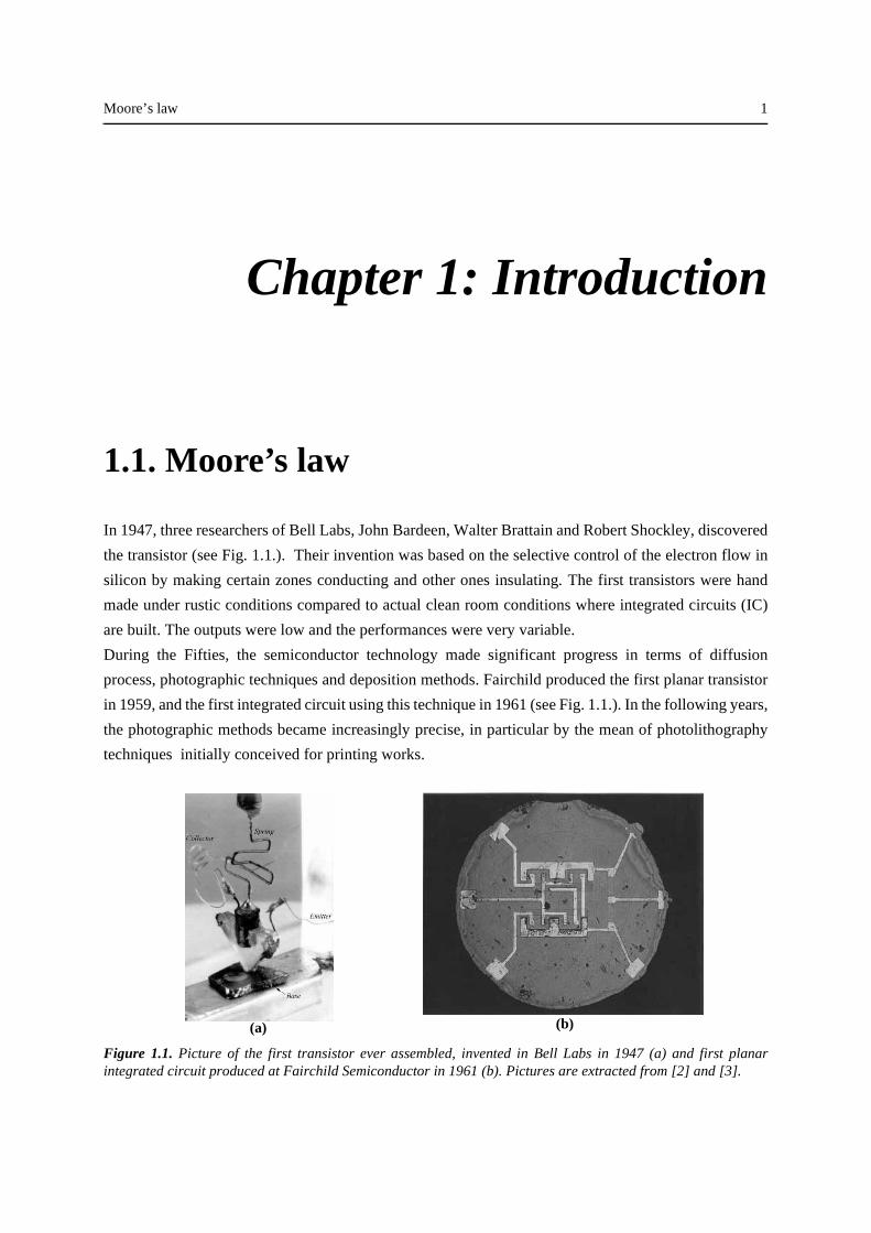
In 1947, three researchers of Bell Labs, John Bardeen, Walter Brattain and Robert Shockley, discovered
the transistor (see Fig. 1.1.). Their invention was based on the selective control of the electron flow in
silicon by making certain zones conducting and other ones insulating. The first transistors were hand
made under rustic conditions compared to actual clean room conditions where integrated circuits (IC)
are built. The outputs were low and the performances were very variable.
During the Fifties, the semiconductor technology made significant progress in terms of diffusion
process, photographic techniques and deposition methods. Fairchild produced the first planar transistor
in 1959, and the first integrated circuit using this technique in 1961 (see Fig. 1.1.). In the following years,
the photographic methods became increasingly precise, in particular by the mean of photolithography
techniques initially conceived for printing works.
Figure 1.1. Picture of the first transistor ever assembled, invented in Bell Labs in 1947 (a) and first planarintegrated circuit produced at Fairchild Semiconductor in 1961 (b). Pictures are extracted from [2] and [3].
(a) (b)
2 Introduction
Gordon Moore was the research and development (R&D) director of Fairchild Semiconductor.
Preparing a graph for a talk on the evolution of memories performances, he noted a striking tendency:
the capacity of the chips has doubled about each year from 1959 to 1965. He deduced : "The complexity
for minimum components costs has increased at a rate of roughly a factor of two per year. Certainly over
the short term this rate can be expected to continue, if not to increase. Over the long term, the rate of
increase is a bit more uncertain, although there is no reason to believe it will not remain nearly constant
for at least 10 years. That means by 1975, the number of components per integrated circuit for minimal
cost will be 65,000." [1].
The reasoning of Moore is subtile. He considered the relation between average cost of production per
component and complexity of the circuit. This function is initially decreasing and then increasing. There
is thus a level of complexity for which the average cost of a component integrated on the circuit is
minimal (see Fig. 1.2. (a)). Then, Moore noted that this optimal level of complexity is multiplied each
year by two what is also depicted on Fig. 1.2. (b).
Figure 1.2. (a) Relative manufacturing cost per component vs the number of components in the circuits estimatedfor various times, and (b) first Moore’s law plot [1].
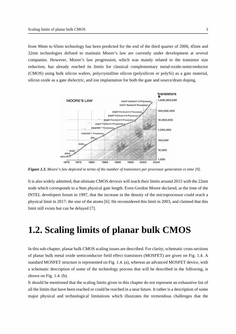
In 1975, Moore revalued the growth rate [4]. Till this moment he considered that three factors are
responsible for the increase of the number of components per chip: (i) the area of the integrated
structures; (ii) the use of finer lithography techniques; and (iii) the device and circuit clever design. From
now on, he said, the latter will have less significant contribution, and the complexity of integrated
circuits would double every two years only and not every year; nevertheless it will remain exponential.
What is astonishing is that in 1995 [5] and 2003 [7], Moore checked that the progression envisaged had
indeed been respected. It is even more obvious when looking at the very last INTEL processor
commercialized at the time of redaction (July 2006), the dual core Itanium 2 "Montecito" which counts
1.72 billion transistors per chip [8] (see dark square on the upper right part of Fig. 1.3.). Fig. 1.3.
describes the evolution of the INTEL processors in terms of number of transistors per processors vs time
and shows this evolution being now exponential over more than fourty years. Furthermore, as the leaping
(a) (b)
Scaling limits of planar bulk CMOS 3
from 90nm to 65nm technology has been predicted for the end of the third quarter of 2006, 45nm and
32nm technologies defined to maintain Moore’s law are currently under development at several
companies. However, Moore’s law progression, which was mainly related to the transistor size
reduction, has already reached its limits for classical complementary metal-oxide-semiconductor
(CMOS) using bulk silicon wafers, polycrystalline silicon (polysilicon or polySi) as a gate material,
silicon oxide as a gate dielectric, and ion implantation for both the gate and source/drain doping.
Figure 1.3. Moore’s law depicted in terms of the number of transistors per processor generation vs time [9].
It is also widely admitted, that ultimate CMOS devices will reach their limits around 2015 with the 22nm
node which corresponds to a 9nm physical gate length. Even Gordon Moore declared, at the time of the
INTEL developers forum in 1997, that the increase in the density of the microprocessor could reach a
physical limit in 2017: the size of the atoms [6]. He reconsidered this limit in 2003, and claimed that this
limit still exists but can be delayed [7].
1.2. Scaling limits of planar bulk CMOS
In this sub-chapter, planar bulk CMOS scaling issues are described. For clarity, schematic cross-sections
of planar bulk metal oxide semiconductor field effect transistors (MOSFET) are given on Fig. 1.4. A
standard MOSFET structure is represented on Fig. 1.4. (a), whereas an advanced MOSFET device, with
a schematic description of some of the technology process that will be described in the following, is
shown on Fig. 1.4. (b).
It should be mentioned that the scaling limits given in this chapter do not represent an exhaustive list of
all the limits that have been reached or could be reached in a near future. It rather is a description of some
major physical and technological limitations which illustrates the tremendous challenges that the
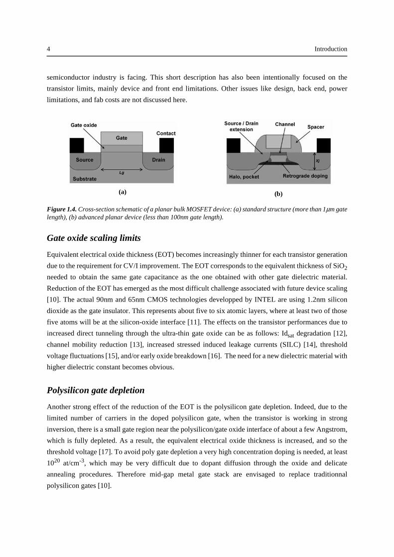
4 Introduction
semiconductor industry is facing. This short description has also been intentionally focused on the
transistor limits, mainly device and front end limitations. Other issues like design, back end, power
limitations, and fab costs are not discussed here.
Figure 1.4. Cross-section schematic of a planar bulk MOSFET device: (a) standard structure (more than 1µm gatelength), (b) advanced planar device (less than 100nm gate length).
Gate oxide scaling limits
Equivalent electrical oxide thickness (EOT) becomes increasingly thinner for each transistor generation
due to the requirement for CV/I improvement. The EOT corresponds to the equivalent thickness of SiO2
needed to obtain the same gate capacitance as the one obtained with other gate dielectric material.
Reduction of the EOT has emerged as the most difficult challenge associated with future device scaling
[10]. The actual 90nm and 65nm CMOS technologies developped by INTEL are using 1.2nm silicon
dioxide as the gate insulator. This represents about five to six atomic layers, where at least two of those
five atoms will be at the silicon-oxide interface [11]. The effects on the transistor performances due to
increased direct tunneling through the ultra-thin gate oxide can be as follows: Idsat degradation [12],
channel mobility reduction [13], increased stressed induced leakage currents (SILC) [14], threshold
voltage fluctuations [15], and/or early oxide breakdown [16]. The need for a new dielectric material with
higher dielectric constant becomes obvious.
Polysilicon gate depletion
Another strong effect of the reduction of the EOT is the polysilicon gate depletion. Indeed, due to the
limited number of carriers in the doped polysilicon gate, when the transistor is working in strong
inversion, there is a small gate region near the polysilicon/gate oxide interface of about a few Angstrom,
which is fully depleted. As a result, the equivalent electrical oxide thickness is increased, and so the
threshold voltage [17]. To avoid poly gate depletion a very high concentration doping is needed, at least
1020 at/cm-3, which may be very difficult due to dopant diffusion through the oxide and delicate
annealing procedures. Therefore mid-gap metal gate stack are envisaged to replace traditionnal
polysilicon gates [10].
(a) (b)
Scaling limits of planar bulk CMOS 5
Parasitic resistances
The ideal scaling theory [18] predicts that the channel resistance, Rchan, should remain constant as the
device, i.e. the channel length, dimensions are reduced. However, due to the higher performances
required for each new technology generation, the ideal scaling theory has not been followed in the last
fourty years and will not likely be followed in the future [16]. Higher performance is achieved by higher
current drive capability and, therefore, Rchan has been dramatically decreased as the technology has been
scaled. Furthermore, the decreasing of the junction depth [19], and the use of smaller contacts [20] has
lead to a large increase of the parasitic resistances. Because of those two parrallel effects, the parasitic
resistances are now becoming comparable, and on course of being even larger than the intrinsic device
resistance. As a result the ON current characteristic of the transistor, Ion, can be brutally degradated [21].
Short channel effects
Short channel effects (SCE) is an important feature of MOSFET with gate lengths shorter than 0.1µm
working at small drain voltages, Vds. At such dimensions the electrostatic potential along the channel
becomes two dimensionnal (2D), instead of 1D for longer channels [22]. Source and drain are standing
at each side of the channel, just few tenth of nanometer from each other, having a strong influence on the
electrostatic potential distribution in the channel . The consequences of un-controlled SCE is a lack of
control on the threshold voltage, Vt : decrease of Vt , and increase of the OFF state current, Ioff. The
retrograde channel doping can not control SCEs and therefore non uniform lateral doping called
superhalo doping is used [23]. Nevertheless, as the channel length Lg, is further reduced very abrupt
doping concentrations are needed [17], which dictates critical and absolutely minimum thermal cycles
after ion implantation [24].
Drain induced barrier lowering
Drain induced barrier lowering (DIBL) is another physical effect due to the short Lg and the 2D
electrostatic potential in small devices, but it appears at higher Vds value than those involved in SCE.
When a bias is applied to the drain, the barrier between source and drain is lowered because of the 2D
eletrostatic potential distribution leading to a lack of control, a decrease of Vt and so, an increase of Ioff.
Nevertheless, DIBL seems to be less important issue than SCE [25].
Channel engineering
High channel doping
The maintenance of acceptable off-state leakage current and SCEs with continually decreasing channel
lenghts will require channel doping levels for planar CMOS transistors to increase for extremely small
devices. The key of doping and annealing are maintaining shallow junction profiles, junction abruptness,
6 Introduction
obtaining high dopant activation, ensuring thermal compatibility of materials, and controlling the impact
of these issues on device electrical performance. This leads to the use, development and even research
of innovative technologies, like: super-steep retrograde and steep halo doping, spike, msec and µsec
anneal, and/or solid phase epitaxy [10].
Dopant fluctuation
With the channel length being today shorter than 50nm, the traditionnal way of describing
semiconductor devices assuming continuous ionised dopant charge and smooth boundaries and
interfaces, is no longer valid. Indeed, the variation in number and position of dopant atoms in the active
region of transistors makes each device microscopically different, and already introduces significant
variations from device to device [26]. Threshold voltage variations as high as 20 to 40mV can appear in
devices with Lg varying from 50 to 10nm respectively [27]. The granularity of electric charge and
atomicity of matter (a 50x50nm MOSFET with channel doping of 5x1018 cm-3 has, on average, 170
atoms in the channel depletion region [28]) should then be introduced as they create substantial variation
in individual device characteristics.
Lithography limits
Three main constituents of the technology improvements that have allowed the semiconductor industry
to follow Moore’s law for more than fourty years are: increased wafer size, smart design, and
lithography. Roughly half of the density improvements can be attributed to improvements in lithography
[29], making it one of the major driver of the semiconductor industry, at least for the last four decades.
ArF scanners (193nm) with a numerical aperture (NA) larger than 0.85 are used in most of the actual
65nm technologies [30]. Nevertheless, as 193nm immersion lithography (with water or other fluids), and
Extreme UV lithography (EUV) developments are underway for the 45nm technology node, there is still
important research needed for the 32, 22 and 16nm nodes. The most probable candidates given by the
ITRS for the post 45nm node being innovative immersion lithography, innovative EUV lithography,
maskless lithography, nanoimprint or other innovative technology [10].
Furthermore, with channel lenghts being shorter than 50nm the lithography must satisfy some key
requirements [10]: i) the size of many features in a design needs to be precisely controlled (CD control);
ii) the placement of the image with respect to underlying layers needs to be accurate on each integrated
circuit in all locations to achieve adequate yield; iii) the desired pattern should present in all locations,
and no additional patterns should be present (defect control); iv) the cost of tools, resist and masks needs
to be as low as possible. One can easely understand that lithography is facing massive challenges, and
while lithography has long helped significantly reduce cost per function of integrated circuits,
maintaining historical levels of cost control and return-on-investment are becoming increasingly
difficult.
More Moore 7
1.3. More Moore
Even though all limitations to further scaling of standard planar bulk CMOS have not been described in
the previous chapter it is obvious that the semiconductor industry will have to solve major challenges in
a very near future. In order to be able to follow the same exponential growth of the last four decades, the
leading manufacturers as well as academic communities are pursuing two directions: (i) evolutionary
CMOS that addresses nanoscale challenges by new materials and device engineering, and (ii) non-
classical CMOS which includes multi-gate devices, ultra-thin body (UTB) silicon on insulator (SOI) and
vertical transistors. This leads to alternative single-gate nonclassical devices using innovative materials
like high-K dielectrics, metal gates and/or strained silicon, but also alternative multiple-gate nonclassical
MOSFET devices with innovative architectures like double, triple gate and/or vertical MOSFETs. This
so-called "more Moore" orientation of research is described below.
1.3.1. Single-gate nonclassical CMOS
Single-gate nonclassical CMOS main research and developments are focused on novel front-end
materials for gate (better electrostatic control of the channel), gate dielectric (improved gate leakage),
channel (improved carrier transport), and source/drain contacts (reduced resistance and improved carrier
injection).
Channel engineered MOSFETS
Agressively scaled CMOS suffer from lack of current drive (Ion) due to mobility degradation induced by
charge scattering in nanometer scaled gate length devices. A powerfull technique to improve MOSFET
performances is to increase the device current drive (the average velocity of the carriers in the channel)
using mechanically strained Si, Ge or SiGE layers. The two principal techniques in strained silicon
technology are descibed on Fig. 1.5.
The first one is the biaxial tensile strain technique using graded SiGe layer (Fig. 1.5. (a)). This traditional
method can be used for both electron and hole mobility enhancement [32]-[38]. Biaxially strained Si
channels standing upon a stack of buried SiGe layers with variable stochiometry and strain conditions,
can improve mobility for both electrons [32], [38] and holes [34] by 85%. The drawback of biaxial stress
is that PMOS shows very low hole mobility enhancement at large vertical electric fields, similar to those
encountered for commercial MOSFETs [39].
The second technique is the uniaxial stress. With this method, n-type and p-type MOSFETs are not using
the same process as shown on Fig. 1.5. (b) and (c). Nevertheless, this technology is already used in
INTEL’s 90nm [40]-[41], and 65nm [42] logic technology, and is foreboded by Fujitsu [43] and Toshiba
8 Introduction
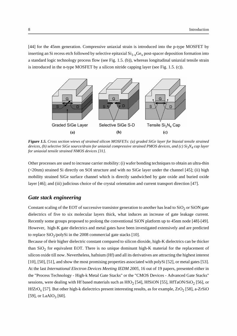
[44] for the 45nm generation. Compressive uniaxial strain is introduced into the p-type MOSFET by
inserting an Si recess etch followed by selective epitaxial Si1-xGex post-spacer deposition formation into
a standard logic technology process flow (see Fig. 1.5. (b)), whereas longitudinal uniaxial tensile strain
is introduced in the n-type MOSFET by a silicon nitride capping layer (see Fig. 1.5. (c)).
Figure 1.5. Cross section wiews of strained silicon MOSFETs: (a) graded SiGe layer for biaxial tensile straineddevices, (b) selective SiGe source/drain for uniaxial compressive strained PMOS devices, and (c) Si3N4 cap layerfor uniaxial tensile strained NMOS devices [31].
Other processes are used to increase carrier mobility: (i) wafer bonding techniques to obtain an ultra-thin
(<20nm) strained Si directly on SOI structure and with no SiGe layer under the channel [45]; (ii) high
mobility strained SiGe surface channel which is directly sandwiched by gate oxide and buried oxide
layer [46]; and (iii) judicious choice of the crystal orientation and current transport direction [47].
Gate stack engineering
Constant scaling of the EOT of successive transistor generation to another has lead to SiO2 or SiON gate
dielectrics of five to six molecular layers thick, what induces an increase of gate leakage current.
Recently some groups proposed to prolong the conventional SiON platform up to 45nm node [48]-[49].
However, high-K gate dielectrics and metal gates have been investigated extensively and are predicted
to replace SiO2/polySi in the 2008 commercial gate stacks [10].
Because of their higher dielectric constant compared to silicon dioxide, high-K dielectrics can be thicker
than SiO2 for equivalent EOT. There is no unique dominant high-K material for the replacement of
silicon oxide till now. Nevertheless, hafnium (Hf) and all its derivatives are attracting the highest interest
[10], [50], [51], and show the most promising properties associated with polySi [52], or metal gates [53].
At the last International Electron Devices Meeting IEDM 2005, 16 out of 19 papers, presented either in
the "Process Technology - High-k Metal Gate Stacks" or the "CMOS Devices - Advanced Gate Stacks"
sessions, were dealing with Hf based materials such as HfO2 [54], HfSiON [55], HfTaON/SiO2 [56], or
HfZrOx [57]. But other high-k dielectrics present interesting results, as for example, ZrO2 [58], a-ZrSiO
[59], or LaAlO3 [60].
(a) (b) (c)
More Moore 9
The metal gate technology has also been intensively investigated for the further improvement of CMOS
performance. The metal should have the appropriate workfunction (WF) for both n-type and p-type FETs
with respect to the gate dielectric. Therefore, many different metals can replace polySi in future
advanced devices, among them are: (i) pure metals like Pt [58] and Mo [59]-[60]; (ii) binary metals such
as TiNx [53]-[55], TaN [56], TaxCy [57],[61]; and (iii) silicided metals (FUSI, FUGESI) like HfSix [62],
TaSix [63], NiSix [64]-[67], YbSix and IrSix [68], NixTa1-xSi and NixPt1-xSi [69], which WF can easily
tuned by a controlled doping. It appears obvious that research, but also development of new gate stack
technologies are still going on today, as no highly stable and performant solutions have yet been found
to replace neither polySi, nor SiON.
Ultra-thin body MOSFETs
To scale bulk MOSFETs down to 10nm gate lengths without excessive SCE , both gate dielectric and
depletion width in silicon must be reduced in proportion with Lg. As shown before, the gate dielectric
reduction can be controlled thanks to new high-k materials, however narrowing down the depletion
width in silicon would require an increased and difficult to control doping of the channel (dopant
fluctuation, decreased mobility). UTB SOI MOSFETs have the potential to bring the semiconductor
industry down to less than 10nm gate lenghts [71].
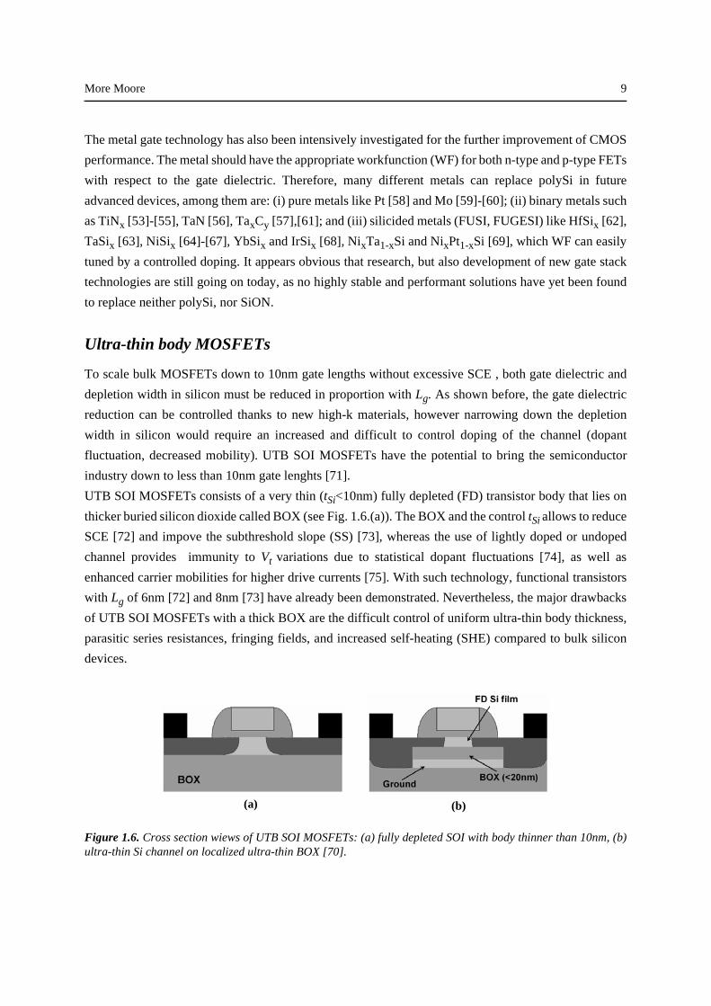
UTB SOI MOSFETs consists of a very thin (tSi<10nm) fully depleted (FD) transistor body that lies on
thicker buried silicon dioxide called BOX (see Fig. 1.6.(a)). The BOX and the control tSi allows to reduce
SCE [72] and impove the subthreshold slope (SS) [73], whereas the use of lightly doped or undoped
channel provides immunity to Vt variations due to statistical dopant fluctuations [74], as well as
enhanced carrier mobilities for higher drive currents [75]. With such technology, functional transistors
with Lg of 6nm [72] and 8nm [73] have already been demonstrated. Nevertheless, the major drawbacks
of UTB SOI MOSFETs with a thick BOX are the difficult control of uniform ultra-thin body thickness,
parasitic series resistances, fringing fields, and increased self-heating (SHE) compared to bulk silicon
devices.
Figure 1.6. Cross section wiews of UTB SOI MOSFETs: (a) fully depleted SOI with body thinner than 10nm, (b)ultra-thin Si channel on localized ultra-thin BOX [70].
(a) (b)
10 Introduction
The localized and ultra-thin BOX MOSFET also called the silicon-on-nothing (SON) MOSFET is an
UTB SOI-like field effect transistor (FET) in which the thin silicon channel is locally isolated from the
bulk-Si substrate by a 10-30nm buried dielectric layer or void as shown on Fig. 1.6. (b). This device has
the same advantages of FD UTB SOI transistor: excellent SS and carrier mobility, reduced SCEs, no
floating body effects; but combined with those of bulk silicon devices: lower series resistances, better
heat dissipation. In addition, SON provides a good control of the silicon film thickness, fringing fields,
and halo profiles [76]-[78]. Very recently, a novel nanoscaled device concept, which also combines both
the advantages of UTB SOI and bulk transistors, named Quasi-SOI MOSFET, has been proposed [79],
[80].
Source/Drain engineered MOSFETS
As seen previously, when the device gate length is scaled down to sub-65nm and further, parasitic source
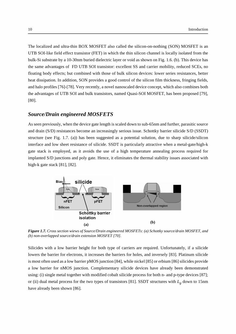
and drain (S/D) resistances become an increasingly serious issue. Schottky barrier silicide S/D (SSDT)
structure (see Fig. 1.7. (a)) has been suggested as a potential solution, due to sharp silicide/silicon
interface and low sheet resistance of silicide. SSDT is particularly attractive when a metal-gate/high-k
gate stack is employed, as it avoids the use of a high temperature annealing process required for
implanted S/D junctions and poly gate. Hence, it eliminates the thermal stability issues associated with
high-k gate stack [81], [82].
Figure 1.7. Cross section wiews of Source/Drain engineered MOSFETs: (a) Schottky source/drain MOSFET, and(b) non-overlapped source/drain extension MOSFET [70].
Silicides with a low barrier height for both type of carriers are required. Unfortunately, if a silicide
lowers the barrier for electrons, it increases the barriers for holes, and inversely [83]. Platinum silicide
is most often used as a low barrier pMOS junction [84], while nickel [85] or erbium [86] silicides provide
a low barrier for nMOS junction. Complementary silicide devices have already been demonstrated
using: (i) single metal together with modified cobalt silicide process for both n- and p-type devices [87];
or (ii) dual metal process for the two types of transistors [81]. SSDT structures with Lg down to 15nm
have already been shown [86].
(b)(a)
More Moore 11
Fig. 1.7. (b) shows the second type of structures (non-overlapped S/D extension MOSFET) that allows
a reduction of the series parasitic resistances, but also parasitic capacitances (fringing and overlap
capacitances). MOSFETs with non-overlapped S/D to gate structure show good SS and SCE/DIBL [88]
compared to those of overlapped structures. By controling the non-overlap distance, the device also
shows reasonable speed [89], and on-current characteristics [90].
1.3.2. Multiple-gate nonclassical CMOS
Compared with single-gate nonclassical CMOS, multiple-gate nonclassical CMOS research is focalized
on innovative device architectures like double gate (DG), triple gate (Tri-gate), and gate all-around
(GAA) MOSFETs. The use of multiple gates for very short channel devices allows a better electrostatic
control of the channel which leads to higher current drive, improved SCE and SS without high impurity
concentration doping [91]. In the last roadmap edition of 2005 [10], the ITRS predicts that UTB FD SOI
and multiple gate MOSFETs will be implemented in 2008 (or later) in parallel with extedend planar bulk
CMOS. This multiple parallel path scenario reflects the fact that some companies will choose to extend
planar bulk CMOS as long as possible, while others will switch to UTB FD SOI and multiple gates
MOSFETs sooner.
Double gate MOSFETs
DG MOSFETs include four different family of devices which can be classified according to the
orientation of the current flow and the type of gate control: (i) the tied gates with planar conduction
device, (ii) the indepedently switched gates with planar conduction transistor, (iii) the vertical
conduction MOSFETs and finally, (iv) the tied gates with side-wall conduction structure, also called
FinFET. All those devices are illustrated on Fig. 1.8.
In planar architectures (Fig. 1.8. (a), (b)), the current flows horizontally between source and drain,
parallel to the plane of the substrate. The fabrication of such devices can be difficult, therefore many
different technologies have been proposed. Among the well known are: the DG realized with SON
process [92], the wafer bonded DG [94], and the so-called PAGODA triple-self-aligned DG [95].
Depending on the technology the top and bottom gate can be self-aligned or not, and NMOS [96], PMOS
[97], and CMOS [98] architectures can be fabricated. The main advantages of DG architectures are
higher current drive, improved SCE and SS. Nevertheless, planar architectures can also show improved
speed [99], better control of the Si channel thickness due to epitaxy [96], and when using asymetric n+/
p+ gates, one can also meliorate the gate induced drain lowering (GIDL) [98], and have better control of
the threshold voltage [100]. Like asymetric DG architectures, DG MOSFETs with independently
controled gates allow dynamic control of Vt leading to lower off currents [101], [102].
In the vertical MOSFET, also called IMOSFET (Fig. 1.8. (c)), the current flows between source and
drain in the vertical direction, orthogonally to the plane of the substrate. The two gates are parallel to the
12 Introduction
plane of the substrate, whereas source and drain stand perpendicularly to it. The main advantage of the
IMOSFET is the control of the gate width (channel length), that is determined by the accuracy of ion
implantation or epitaxial growth (the gate width is not controlled by lithography). It is then recognized
that vertical transistors can be a credible candidate for sub-100nm devices [103]. Various type of
innovative device (process) have been proposed: 50nm vertical MOSFET incorporating a dielectric
pocket [104]; heterogeneous Si0.70Ge0.30/Si0.85Ge0.15 pMOSFET [105]; 50nm Vertical Replacement-
Gate (VRG) MOSFET using high-k gate dielectrics [106]; vertical sidewall device [107]; and Ultrathin
Vertical Channel (UTVC) MOSFET [108]. It is obvious that there is yet no leading vertical MOSFET
technology because of challenging process requirements, and most of the time state-of-the-art vertical
structures underperform advanced planar CMOS. However, 15nm Lg vertical MOSFETs have already
been demonstrated [109], and improved Ion/Ioff performances compared with advanced planar transistors
have been shown for the VRG MOSFET [110].
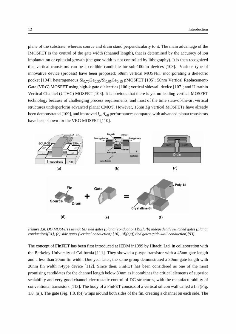
Figure 1.8. DG MOSFETs using: (a) tied gates (planar conduction) [92], (b) indepedently switched gates (planarconduction)[31], (c) side gates (vertical conduction) [10], (d)(e)(f) tied gates (side-wall conduction)[93].
The concept of FinFET has been first introduced at IEDM in1999 by Hitachi Ltd. in collaboration with
the Berkeley University of California [111]. They showed a p-type transistor with a 45nm gate length
and a less than 20nm fin width. One year later, the same group demonstrated a 30nm gate length with
20nm fin width n-type device [112]. Since then, FinFET has been considered as one of the most
promising candidates for the channel length below 30nm as it combines the critical elements of superior
scalability and very good channel electrostatic control of DG structures, with the manufacturability of
conventional transistors [113]. The body of a FinFET consists of a vertical silicon wall called a fin (Fig.
1.8. (a)). The gate (Fig. 1.8. (b)) wraps around both sides of the fin, creating a channel on each side. The
(b)(a) (c)
(d) (e) (f)
More Moore 13
main advantage of the FinFET structure (Fig. 1.8. (c)) is that the two self-aligned gates can be fabricated
using a single lithography and etch step [114]. Contrary to the DG planar devices, the conduction in a
FinFET takes place on the vertical sidewalls of the fin. The major challenge is the fabrication of thin fins
that need to be one third to one half of the gate length in order to have an adequate control of SCEs. Many
devices have been fabricated combining electron beam (e-beam) lithography, and photoresist ashing
techniques followed by oxide hard mask trimming, allowing to reach fin widths of 20nm [115].
Moreover, adapted spacer technology can decrease the fin width down to 10nm and double the fin
density [116]. The fabrication cost is also a big issue of FinFET because most of the fabricated devices
uses complicated process and SOI substrate. Nevertheless, CMOS FinFET fabricated on bulk Si
substrate has already been shown [117]-[118], and many new devices are presented every day: 20nm
gate bulk-FinFET SONOS Flash [119], 10nm gate length FinFET [120], 5nm gate Nanowire FinFET
[121], and high-performance CMOS compatible Vt asymmetric-gate devices [93].
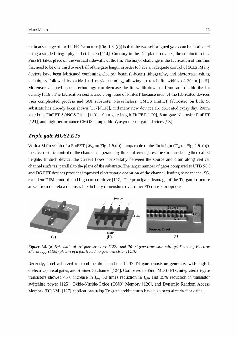
Triple gate MOSFETs
With a Si fin width of a FinFET (WSi on Fig. 1.9.(a)) comparable to the fin height (TSi on Fig. 1.9. (a)),
the electrostatic control of the channel is operated by three different gates, the structure being then called
tri-gate. In such device, the current flows horizontally between the source and drain along vertical
channel surfaces, parallel to the plane of the substrate. The larger number of gates compared to UTB SOI
and DG FET devices provides improved electrostatic operation of the channel, leading to near-ideal SS,
excellent DIBL control, and high current drive [122]. The principal advantage of the Tri-gate structure
arises from the relaxed constraints in body dimensions over other FD transistor options.
Figure 1.9. (a) Schematic of tri-gate structure [122], and (b) tri-gate transistor, with (c) Scanning ElectronMicroscopy (SEM) picture of a fabricated tri-gate transistor [123].
Recently, Intel achieved to combine the benefits of FD Tri-gate transistor geometry with high-k
dielectrics, metal gates, and strained Si channel [124]. Compared to 65nm MOSFETs, integrated tri-gate
transistors showed 45% increase in Ion, 50 times reduction in Ioff, and 35% reduction in transistor
switching power [125]. Oxide-Nitride-Oxide (ONO) Memory [126], and Dynamic Random Access
Memory (DRAM) [127] applications using Tri-gate architectures have also been already fabricated.
(c)(b)(a)
14 Introduction
Ω- and Π-Gate devices described in [128] and [129] respectively, are basically similar to Tri-gate
architectures, but thanks to the extension of the gate below the fin, into the buried oxide, their channel
control is more close to the GAA MOSFET depicted in the next paragraph.
Gate all-around MOSFETs
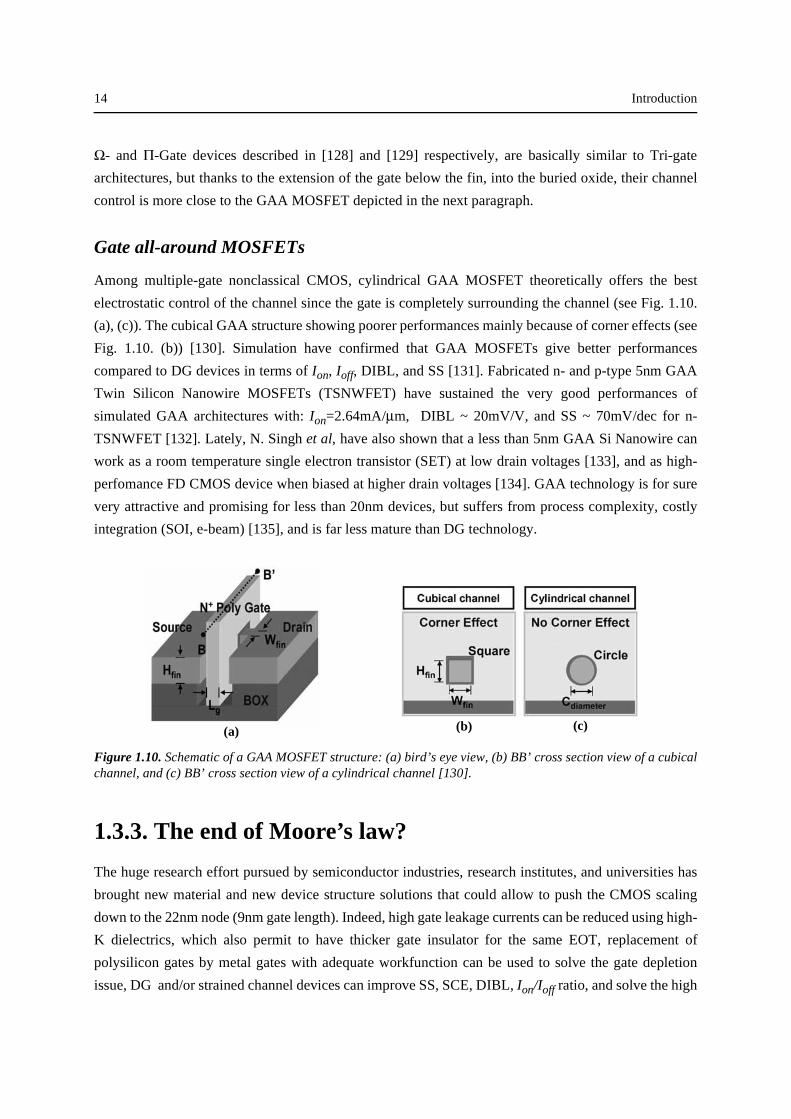
Among multiple-gate nonclassical CMOS, cylindrical GAA MOSFET theoretically offers the best
electrostatic control of the channel since the gate is completely surrounding the channel (see Fig. 1.10.
(a), (c)). The cubical GAA structure showing poorer performances mainly because of corner effects (see
Fig. 1.10. (b)) [130]. Simulation have confirmed that GAA MOSFETs give better performances
compared to DG devices in terms of Ion, Ioff, DIBL, and SS [131]. Fabricated n- and p-type 5nm GAA
Twin Silicon Nanowire MOSFETs (TSNWFET) have sustained the very good performances of
simulated GAA architectures with: Ion=2.64mA/µm, DIBL ~ 20mV/V, and SS ~ 70mV/dec for n-
TSNWFET [132]. Lately, N. Singh et al, have also shown that a less than 5nm GAA Si Nanowire can
work as a room temperature single electron transistor (SET) at low drain voltages [133], and as high-
perfomance FD CMOS device when biased at higher drain voltages [134]. GAA technology is for sure
very attractive and promising for less than 20nm devices, but suffers from process complexity, costly
integration (SOI, e-beam) [135], and is far less mature than DG technology.
Figure 1.10. Schematic of a GAA MOSFET structure: (a) bird’s eye view, (b) BB’ cross section view of a cubicalchannel, and (c) BB’ cross section view of a cylindrical channel [130].
1.3.3. The end of Moore’s law?
The huge research effort pursued by semiconductor industries, research institutes, and universities has
brought new material and new device structure solutions that could allow to push the CMOS scaling
down to the 22nm node (9nm gate length). Indeed, high gate leakage currents can be reduced using high-
K dielectrics, which also permit to have thicker gate insulator for the same EOT, replacement of
polysilicon gates by metal gates with adequate workfunction can be used to solve the gate depletion
issue, DG and/or strained channel devices can improve SS, SCE, DIBL, Ion/Ioff ratio, and solve the high
(a) (b) (c)
More Moore 15
channel doping challenges and dopant fluctuations issues; finally, metallic elevated S/D junctions reduce
the access resistance and eliminate the very steep highly doped junction problems.
Furthermore, 10nm has been predicted to be the fundamental limit for MOSFET operation for many
years [136], however functionnal 5nm Lg planar bulk CMOS devices [137], and 6nm Lg planar SOI
single-gate p-type MOSFETs [72] have been demonstrated, which gives hope for the 16nm node (6nm
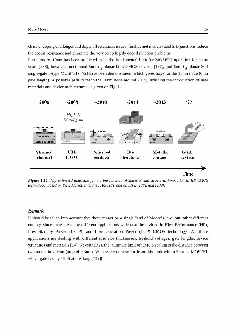
gate length). A possible path to reach the 16nm node around 2019, including the introduction of new
materials and device architectures, is given on Fig. 1.11.
Figure 1.11. Approximated timescale for the introduction of material and structural innovation in HP CMOStechnology, based on the 2005 edtion of the ITRS [10], and on [31], [138], and [139].
Remark
It should be taken into account that there cannot be a single "end of Moore’s law" but rather different
endings since there are many different applications which can be divided in High Performance (HP),
Low Standby Power (LSTP), and Low Operation Power (LOP) CMOS technology. All these
applications are dealing with different insulator thicknesses, treshold voltages, gate lengths, device
structures and materials [24]. Nevertheless, the ultimate limit of CMOS scaling is the distance between
two atoms in silicon (around 0.3nm). We are then not so far from this limit with a 5nm Lg MOSFET
which gate is only 18 Si atoms long [139]!
16 Introduction
1.4. After Moore (beyond CMOS): emerging nanoelectronics
1.4.1. Overview
We have seen previously, that present 65nm node MOSFET devices have a physical gate length about
30nm. It is also widely admitted that the introduction of new materials and new device architectures
(more Moore) may extend the roadmap at least to the 22nm node (9nm gate length) by 2016. Beyond
that point, the semiconductor industry will have to find fundamentaly new approaches to information,
signal processing, and data-storage. This implies the exploitation of alternative devices, materials, and
process, but also involves systems innovations. These new technologies must satisfy the following [10]:
a) Extend microelectronics orders of magnitude beyond the domain of CMOS, and be capable of
integration on or with a CMOS platform. This implies:
• Functionally scalable by several orders of magnitude beyond CMOS devices,
• High information/signal processing rate and throughput,
• Energy dissipation per functional operation substantially less than CMOS,
• Minimum scalable cost per function.
b) Room temperature operation.
Many devices and techniques have been proposed as "after Moore" innovative technologies which may
supplant or complement CMOS as the dominent device technology: SETs, Quantum Cellular Automata
(QCA), Carbon Nanotube (CNT) based devices, Rapid Single Flux Quantum (RSFQ) structures,
Nanoelectromechanical Systems (NEMS), resonant tunneling diodes/devices (RTD), Spintronics,
nanowire (NW) devices, or molecular electronics. Nevertheless, many of those technologies are yet not
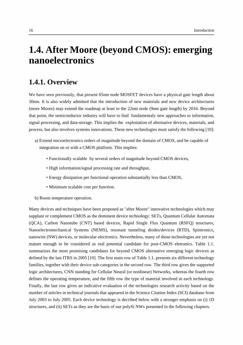
mature enough to be considered as real potential candidate for post-CMOS eletronics. Table 1.1.
summarizes the most promising candidates for beyond CMOS alternative emerging logic devices as
defined by the last ITRS in 2005 [10]. The first main row of Table 1.1. presents six different technology
families, together with their device sub-categories in the second row. The third row gives the supported
logic architectures, CNN standing for Cellular Neural (or nonlinear) Networks, whereas the fourth row
defines the operating temperature, and the fifth row the type of material involved in each technology.
Finally, the last row gives an indicative evaluation of the technologies research activity based on the
number of articles in technical journals that appeared in the Science Citation Index (SCI) database from
July 2003 to July 2005. Each device technology is decribed below with a stronger emphasis on (i) 1D
structures, and (ii) SETs as they are the basis of our polySi NWs presented in the following chapters.
After Moore (beyond CMOS): emerging nanoelectronics 17
Table 1.1. Emerging research logic devices defined by the 2005 ITRS [10].
Resonant Tunneling Devices
The major advantages of two-terminal RTDs are: (i) a very high switching speed, which can be as low
as 1.5ps [140], and (ii) a Negative Differential Resistance (NDR) region in the I-V characteristic which
can be used to greatly reduce the circuit complexity required for high-speed logic functions [141]. Three
terminal bipolar resonant tunneling transistors (RTT) can be build, with a pair of RTDs and a control
terminal [142], and thanks to their negative transconductance, RTTs can serve as building block for logic
circuits [143]. Theoretical feasibility of Multiple Valued Logic (MVL) circuits based on p- and n-type
Si RTT has even been already shown [144].
RTDs are usually fabricated in III-V material systems, but recently, few groups have shown Si
compatible fabrication, like three-terminal Si/SiGe-based NDR [143], or Si-based field-induced band-
to-band tunneling effect transistor [145]. Nevertheless, RTD devices suffer from very poor Ion/Ioff ratio
and integration complexity, which can limit the circuit design and the dimensional scaling respectively.
Spintronics
The large interest for spin logic devices probably comes from the fact that spin-dependent transport
properties are already integrated on many magnetic storage media like Magnetic Random Access
Memories (MRAM), hard disks, or read heads. Prior to the 2005 edition of the ITRS, spintronic was
mostly related to the Datta-Das FET current modulator concept [146], but in the last ITRS edition [10],
five other type of spin based devices were introduced: (i) the magneto resistive element device [147], (ii)
the spin-gain transistor [148], (iii) the spin-torque transistor [149], (iv) the hybrid hall effect device
[150], and (v) the spin MOSFET [151]. Those proposed new structures, all based on different operating
principles, testify from the great deal of research activity going on in this field.
18 Introduction
However, spintronics is facing non-negligible issues: no viable device has been demonstrated till date;
co-fabrication with CMOS might not be doable as spintronic devices process involve metal alloys like
Cr, Fe, or Mn; increased device density and speed compared to CMOS may not be achieved, since actual
spintronic devices still rely on charge transport.
Molecular electronics
Molecular research might be the youngest and less mature of the six emerging logic research devices
defined by the ITRS. Even so, it attracts the major interests compared to the five other emerging devices
(see research activity row of Table 1.1). This can be explained by the molecular thrilling properties [10]:
• the electronic properties of organic molecules may be tailored through the chemical
synthesis;
• the reproducibility between organic molecular units is perfect;
• the size of complex molecules is in the order of approximately 1nm, which can lead to
device densities greater than 1012 cm-2;
• organic molecules require few electrons for molecular switching (very low energy);
• and last but not least, molecular switching is a very fast process (THz regime).
Therefore, despite the youth of molecular electronic, many basic devices utilizing molecules such as two
terminal reversible switches [152], tunable resistors with three decade of ohmic range [153], SETs
[154], or large peak to valley ratio NDR [155], have already been demonstrated. Lately, hybrid Silicon/
Molecular FETs have been proposed and fabricated, showing potential for low-voltage, multiple-state
memory and logic applications [156].
Before the introduction of molecules in nowadays electronic circuits, major problems have to be solved.
This include the realization of efficient and reproducible contacts to molecular building blocks, the
design of suitable interconnects and interfaces to the "outside world", and the stabilization of the organic
molecules through multiple cycles (>1010), and CMOS typical thermal processing. Novel very defect-
tolerant architectures and adapted design of devices and circuits would also be very challenging.
Ferromagnetic logic
Contrary to molecular devices, ferromagnetic logic is the emerging research device which attracts the
less interest as one can see on the last row of Table 1.1. However, Magnetic Quantum Cellular Automata
(MQCA) had shown more than promising results in terms of integration density and power dissipation
in 2000 [157]. Moreover, submicrometer ferromagnetic NOT gate had been demonstrated in 2002 [158].
Nevertheless, the major drawback of ferromagnetic logic is the speed which seems to be limited to a
maximum of 1GHz [159].
After Moore (beyond CMOS): emerging nanoelectronics 19
1.4.2. 1D structures
In its 2003 edition of the roadmap, the ITRS declared that 1D structures had greater potential impact on
scaled nanoelectronics than any other entries, even though the difficulties associated with their
introduction into high volume manufacturing were still judged to be important [10]. Many researchers
still believe this point of view in 2006, as the journal Nature, based on the research of Michael Banks
[160], has elected CNTs as the hottest topic in physics, followed by nanowires in the second position
[161]. The tremendous investments in terms of money and research made since 2003, has permitted to
identify the critical issues associated with 1D structures: (i) understand the basic physical mechanisms
in quantum-confined transport; (ii) control and predict the characteristics of nanowires and nanotubes
with fabrication; (iii) control the fabrication in terms of devices placement, contacting, doping, and find
adequate materials for the gate stack; and (iv) being able to characterize device electrical behavior with
already known metrics like e.g. SS, DIBL, Ion/Ioff.
The term 1D structures refers to devices in which the current is flowing quasi-unidirectionnaly from
source to drain, and that have a lateral feature size constrained to tens of nanometers or less, together
with unconstrained longitudinal size. 1D structures include NW heterostructures, and crossbar
nanostructures but the main driving forces are CNTs and NWs as illustrated below.
Carbon nanotube technology
The extremely large success of CNTs can be explained by three different reasons. First of all, as this
material has been discovered very recently it benefits from the effect of novelty and fashion. Secondly,
CNTs have uncomparable physical properties, they exhibit extreme strength, unique electrical properties
(a nanotube can be either metallic or semiconducting), and very good thermal conductivity. Thirdly, they
can be used in many applications going from combat jackets to high frequency oscillators, from artificial
muscles to thin high-brightness low-energy low-weight displays, or from light-weight high-strength
bicycle to air pollution filters.
Many reseachers attributed the discovery of CNTs to Ijima in 1991 [162]. However, the first evidence
of multi-walled CNTs (MWCNT) has been published in 1952 by Radushkevich et al [163]. Afterwards,
in 1993, Ijima [164] and Ichiashi [165] reported for the first time the fabrication of single-walled CNTs
(SWCNT). Since then, almost every day a different CNT based device or application is proposed.
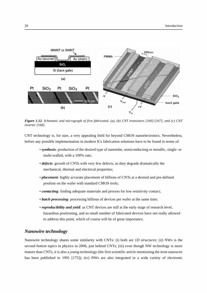
The first fabricated transistors consisting of a nanotube deposited in between two metal pads (source and
drain) and controlled by the bulk Si back gate , were shown in 1998 by IBM [166], and Delft Universisty
[167] (see Fig. 1.12. (a), (b)). Demonstration of CNT logic followed shortly in 2001 with the fabrication
of an inverter (see Fig. 1.12. (c)) [168], a NOR, a SRAM and a ring oscillator cell [169]. Finally, other
electronics applications of CNTs include SETs [170], optics [171], interconnects [172], and NEMS such
as nanorelay [173], or resonators [174].
20 Introduction
Figure 1.12. Schematic and micrograph of first fabricated: (a), (b) CNT transistors [166]-[167], and (c) CNTinverter [168].
CNT technology is, for sure, a very appealing field for beyond CMOS nanoelectronics. Nevertheless,
before any possible implementation in modern ICs fabrication solutions have to be found in terms of:
• synthesis: production of the desired type of nanotube, semiconducting or metallic, single- or
multi-walled, with a 100% rate;
• defects: growth of CNTs with very few defects, as they degrade dramatically the
mechanical, thermal and electrical properties;
• placement: highly accurate placement of billions of CNTs at a desired and pre-defined
position on the wafer with standard CMOS tools;
• contacting: finding adequate materials and process for low resistivity contact;
• batch processing: processing billions of devices per wafer at the same time;
• reproducibility and yield: as CNT devices are still at the early stage of research level,
hazardous positioning, and so small number of fabricated devices have not really allowed
to address this point, which of course will be of great importance.
Nanowire technology
Nanowire technology shares some similarity with CNTs: (i) both are 1D structures; (ii) NWs is the
second hottest topics in physics in 2006, just behind CNTs; (iii) even though NW technology is more
mature than CNTs, it is also a young technology (the first scientific article mentioning the term nanowire
has been published in 1991 [175]); (iv) NWs are also integrated in a wide variety of electronic
(a)
(b) (c)
After Moore (beyond CMOS): emerging nanoelectronics 21
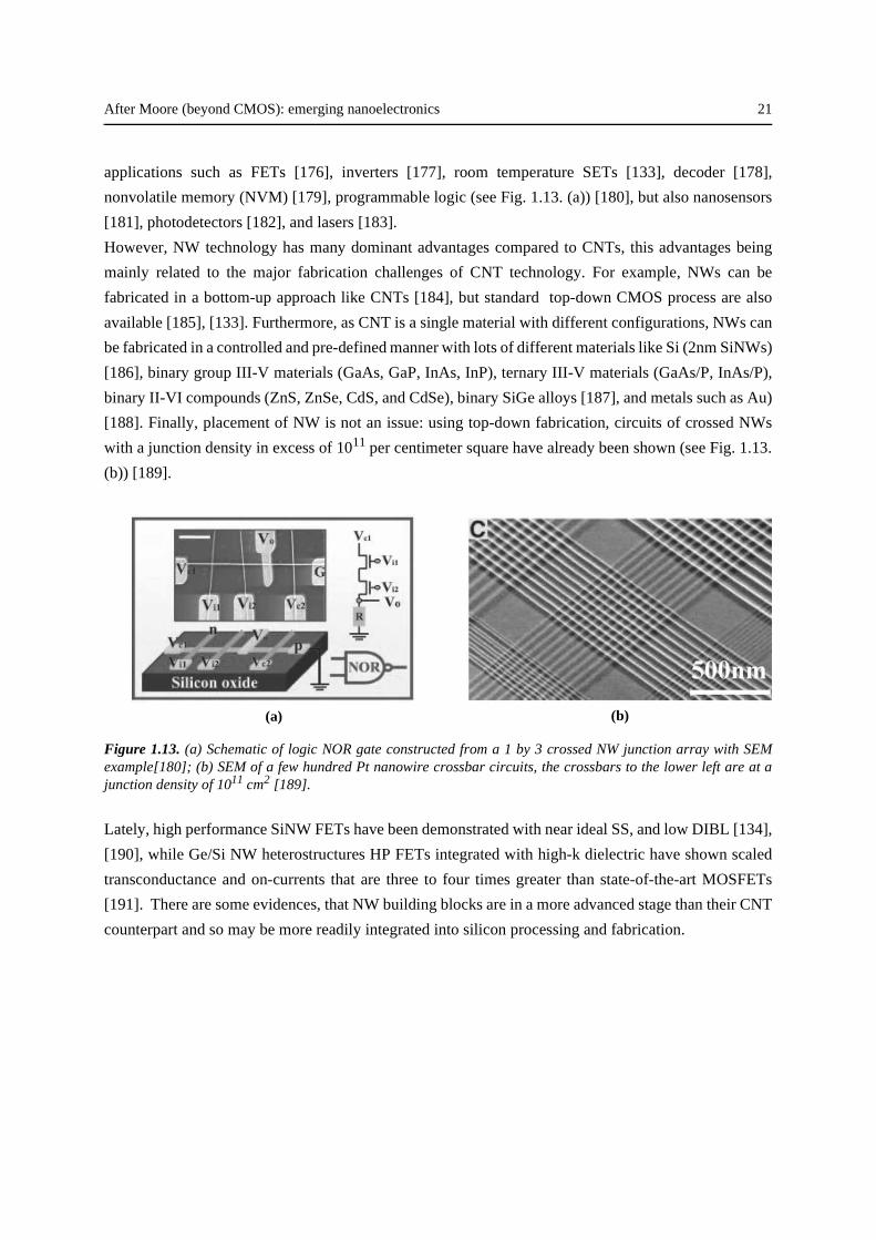
applications such as FETs [176], inverters [177], room temperature SETs [133], decoder [178],
nonvolatile memory (NVM) [179], programmable logic (see Fig. 1.13. (a)) [180], but also nanosensors
[181], photodetectors [182], and lasers [183].
However, NW technology has many dominant advantages compared to CNTs, this advantages being
mainly related to the major fabrication challenges of CNT technology. For example, NWs can be
fabricated in a bottom-up approach like CNTs [184], but standard top-down CMOS process are also
available [185], [133]. Furthermore, as CNT is a single material with different configurations, NWs can
be fabricated in a controlled and pre-defined manner with lots of different materials like Si (2nm SiNWs)
[186], binary group III-V materials (GaAs, GaP, InAs, InP), ternary III-V materials (GaAs/P, InAs/P),
binary II-VI compounds (ZnS, ZnSe, CdS, and CdSe), binary SiGe alloys [187], and metals such as Au)
[188]. Finally, placement of NW is not an issue: using top-down fabrication, circuits of crossed NWs
with a junction density in excess of 1011 per centimeter square have already been shown (see Fig. 1.13.
(b)) [189].
Figure 1.13. (a) Schematic of logic NOR gate constructed from a 1 by 3 crossed NW junction array with SEMexample[180]; (b) SEM of a few hundred Pt nanowire crossbar circuits, the crossbars to the lower left are at ajunction density of 1011 cm2 [189].
Lately, high performance SiNW FETs have been demonstrated with near ideal SS, and low DIBL [134],
[190], while Ge/Si NW heterostructures HP FETs integrated with high-k dielectric have shown scaled
transconductance and on-currents that are three to four times greater than state-of-the-art MOSFETs
[191]. There are some evidences, that NW building blocks are in a more advanced stage than their CNT
counterpart and so may be more readily integrated into silicon processing and fabrication.
(b)(a)
22 Introduction
1.4.3. Single Electron Transistors
C. Gorter was probably the first to introduce single electron electronics in 1951 when he explained for
the first time the Coulomb blockade (CB) phenomenon. Much later, in 1985, D. Averin and K. Likharev
[192] formulated the orthodox theory of single-electron tunneling that describes the charge transport
under the influence of CB and allows the exploitation of SET [193]. Since then, SETs have gained high
interests mainly because: (i) SETs can be scaled down to the nanometer scale making them good
candidate for Ultra Large Scale Integration (ULSI); (ii) thanks to CB, SETs can control the transfer of
electron from source to drain with a one electron or few electron precision and therefore deal with ultra-
low power consumption; (iii) SETs have a large variety of applications, going from logic to memory,
but also electrometry.
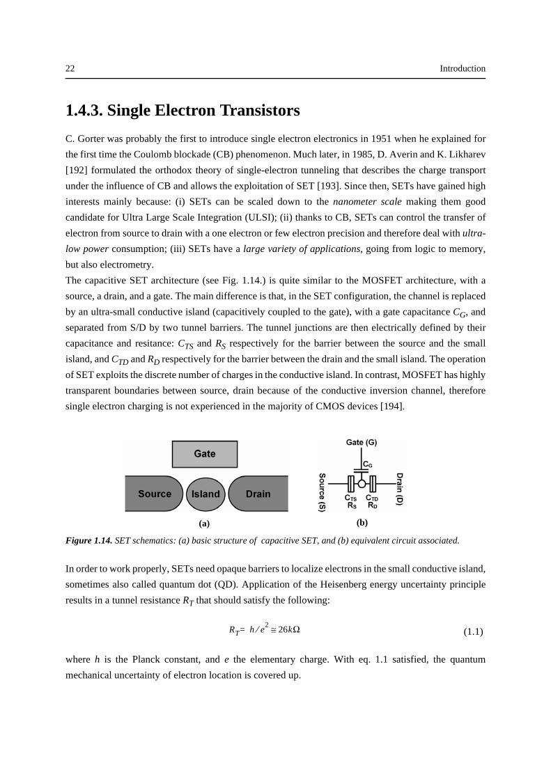
The capacitive SET architecture (see Fig. 1.14.) is quite similar to the MOSFET architecture, with a
source, a drain, and a gate. The main difference is that, in the SET configuration, the channel is replaced
by an ultra-small conductive island (capacitively coupled to the gate), with a gate capacitance CG, and
separated from S/D by two tunnel barriers. The tunnel junctions are then electrically defined by their
capacitance and resitance: CTS and RS respectively for the barrier between the source and the small
island, and CTD and RD respectively for the barrier between the drain and the small island. The operation
of SET exploits the discrete number of charges in the conductive island. In contrast, MOSFET has highly
transparent boundaries between source, drain because of the conductive inversion channel, therefore
single electron charging is not experienced in the majority of CMOS devices [194].
Figure 1.14. SET schematics: (a) basic structure of capacitive SET, and (b) equivalent circuit associated.
In order to work properly, SETs need opaque barriers to localize electrons in the small conductive island,
sometimes also called quantum dot (QD). Application of the Heisenberg energy uncertainty principle
results in a tunnel resistance RT that should satisfy the following:
(1.1)
where h is the Planck constant, and e the elementary charge. With eq. 1.1 satisfied, the quantum
mechanical uncertainty of electron location is covered up.
(a) (b)
RT h e2⁄ 26≅= kΩ
After Moore (beyond CMOS): emerging nanoelectronics 23
In order to have fully functional SET, the charging energy of the island EC must be larger than the
thermal fluctuations:
(1.2)
This condition can be fulfilled either by working at low temperature, T, and/or with very small island to
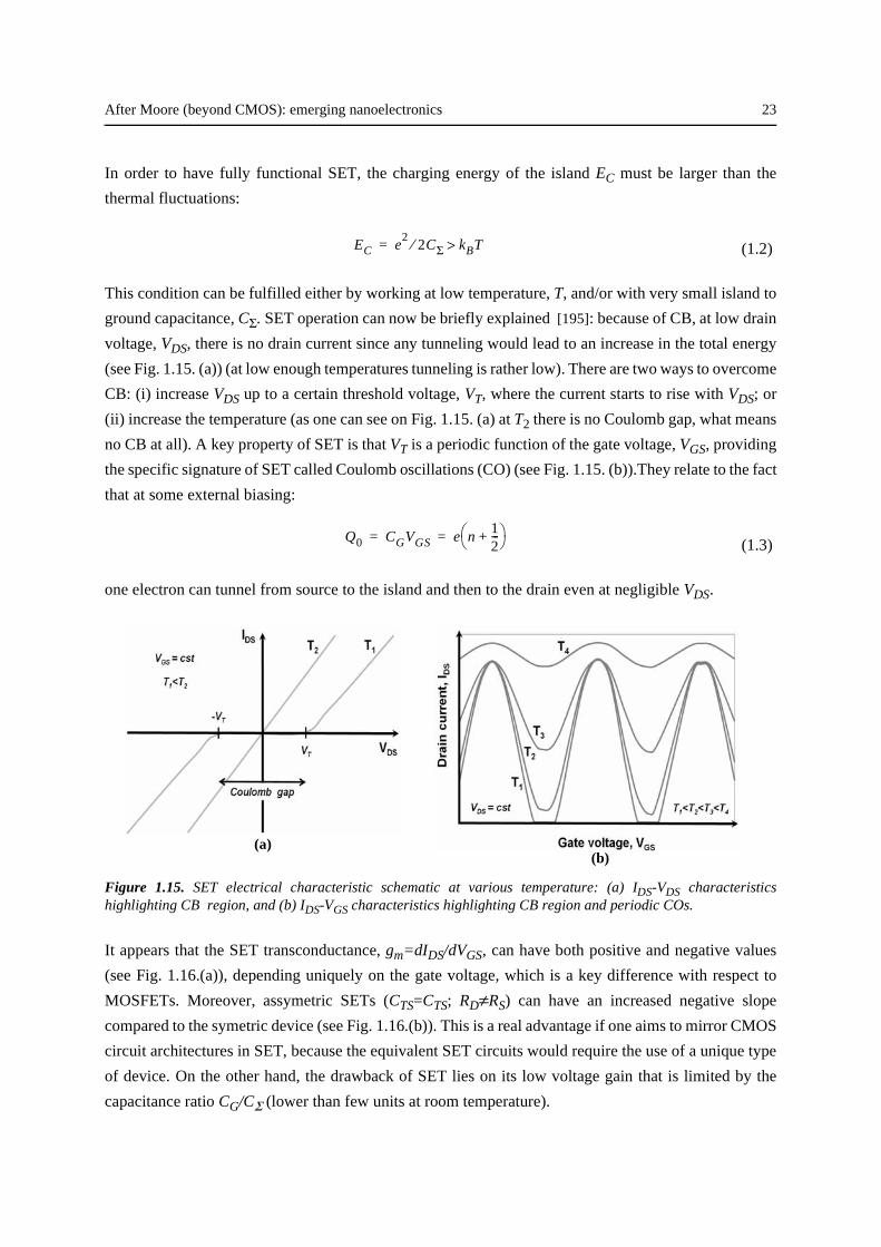
ground capacitance, CΣ. SET operation can now be briefly explained [195]: because of CB, at low drain
voltage, VDS, there is no drain current since any tunneling would lead to an increase in the total energy
(see Fig. 1.15. (a)) (at low enough temperatures tunneling is rather low). There are two ways to overcome
CB: (i) increase VDS up to a certain threshold voltage, VT, where the current starts to rise with VDS; or
(ii) increase the temperature (as one can see on Fig. 1.15. (a) at T2 there is no Coulomb gap, what means
no CB at all). A key property of SET is that VT is a periodic function of the gate voltage, VGS, providing
the specific signature of SET called Coulomb oscillations (CO) (see Fig. 1.15. (b)).They relate to the fact
that at some external biasing:
(1.3)
one electron can tunnel from source to the island and then to the drain even at negligible VDS.
Figure 1.15. SET electrical characteristic schematic at various temperature: (a) IDS-VDS characteristicshighlighting CB region, and (b) IDS-VGS characteristics highlighting CB region and periodic COs.
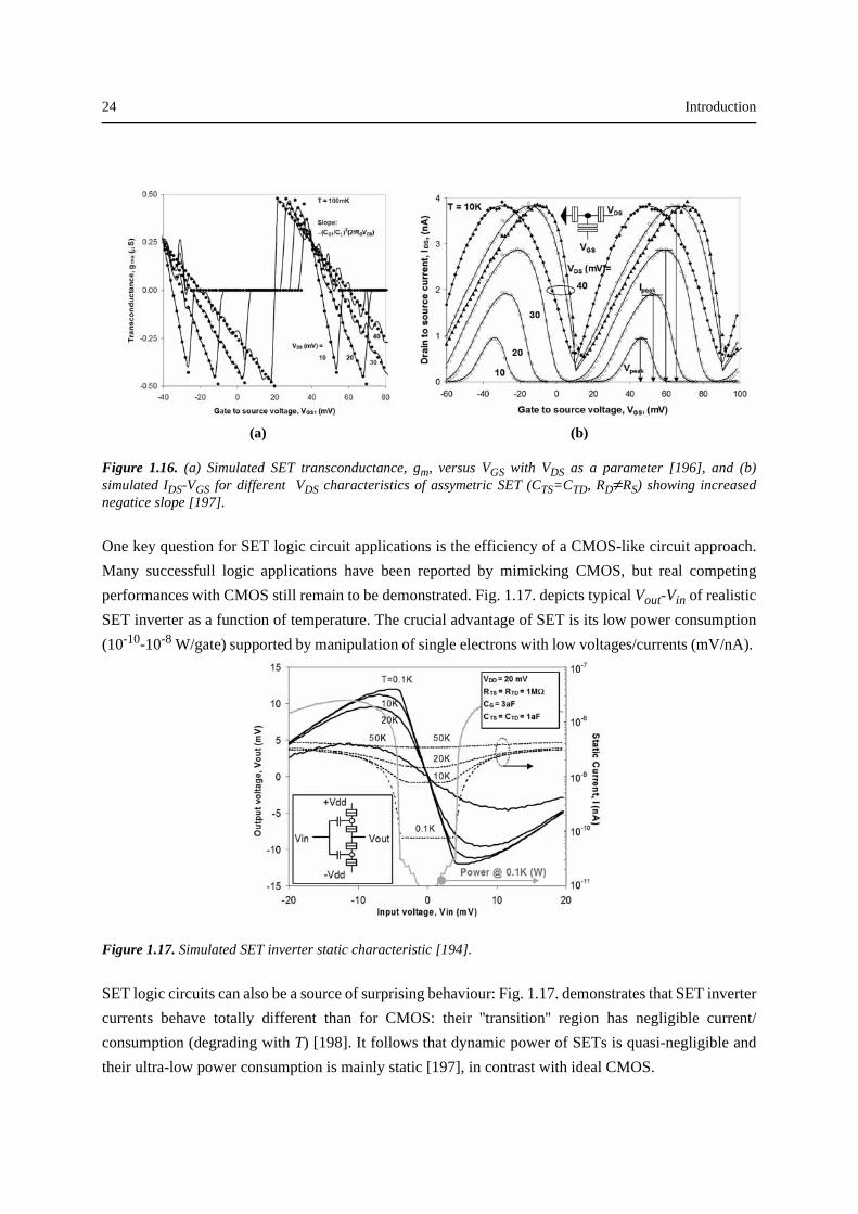
It appears that the SET transconductance, gm=dIDS/dVGS, can have both positive and negative values
(see Fig. 1.16.(a)), depending uniquely on the gate voltage, which is a key difference with respect to
MOSFETs. Moreover, assymetric SETs (CTS=CTS; RD≠RS) can have an increased negative slope
compared to the symetric device (see Fig. 1.16.(b)). This is a real advantage if one aims to mirror CMOS
circuit architectures in SET, because the equivalent SET circuits would require the use of a unique type
of device. On the other hand, the drawback of SET lies on its low voltage gain that is limited by the
capacitance ratio CG/CΣ (lower than few units at room temperature).
EC e2
2CΣ kBT>⁄=
Q0 CGVGS e n12---+⎝ ⎠
⎛ ⎞= =
(a)(b)
24 Introduction
Figure 1.16. (a) Simulated SET transconductance, gm, versus VGS with VDS as a parameter [196], and (b)simulated IDS-VGS for different VDS characteristics of assymetric SET (CTS=CTD, RD≠RS) showing increasednegatice slope [197].
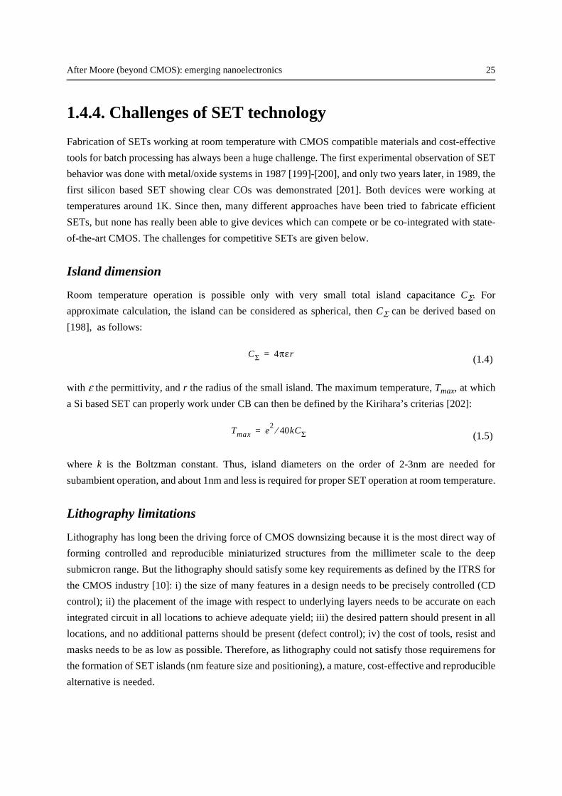
One key question for SET logic circuit applications is the efficiency of a CMOS-like circuit approach.
Many successfull logic applications have been reported by mimicking CMOS, but real competing
performances with CMOS still remain to be demonstrated. Fig. 1.17. depicts typical Vout-Vin of realistic
SET inverter as a function of temperature. The crucial advantage of SET is its low power consumption
(10-10-10-8 W/gate) supported by manipulation of single electrons with low voltages/currents (mV/nA).
Figure 1.17. Simulated SET inverter static characteristic [194].
SET logic circuits can also be a source of surprising behaviour: Fig. 1.17. demonstrates that SET inverter
currents behave totally different than for CMOS: their ''transition'' region has negligible current/
consumption (degrading with T) [198]. It follows that dynamic power of SETs is quasi-negligible and
their ultra-low power consumption is mainly static [197], in contrast with ideal CMOS.
(a) (b)
After Moore (beyond CMOS): emerging nanoelectronics 25
1.4.4. Challenges of SET technology
Fabrication of SETs working at room temperature with CMOS compatible materials and cost-effective
tools for batch processing has always been a huge challenge. The first experimental observation of SET
behavior was done with metal/oxide systems in 1987 [199]-[200], and only two years later, in 1989, the
first silicon based SET showing clear COs was demonstrated [201]. Both devices were working at
temperatures around 1K. Since then, many different approaches have been tried to fabricate efficient
SETs, but none has really been able to give devices which can compete or be co-integrated with state-
of-the-art CMOS. The challenges for competitive SETs are given below.
Island dimension
Room temperature operation is possible only with very small total island capacitance CΣ. For
approximate calculation, the island can be considered as spherical, then CΣ can be derived based on
[198], as follows:
(1.4)
with ε the permittivity, and r the radius of the small island. The maximum temperature, Tmax, at which
a Si based SET can properly work under CB can then be defined by the Kirihara’s criterias [202]:
(1.5)
where k is the Boltzman constant. Thus, island diameters on the order of 2-3nm are needed for
subambient operation, and about 1nm and less is required for proper SET operation at room temperature.
Lithography limitations
Lithography has long been the driving force of CMOS downsizing because it is the most direct way of
forming controlled and reproducible miniaturized structures from the millimeter scale to the deep
submicron range. But the lithography should satisfy some key requirements as defined by the ITRS for
the CMOS industry [10]: i) the size of many features in a design needs to be precisely controlled (CD
control); ii) the placement of the image with respect to underlying layers needs to be accurate on each
integrated circuit in all locations to achieve adequate yield; iii) the desired pattern should present in all
locations, and no additional patterns should be present (defect control); iv) the cost of tools, resist and
masks needs to be as low as possible. Therefore, as lithography could not satisfy those requiremens for
the formation of SET islands (nm feature size and positioning), a mature, cost-effective and reproducible
alternative is needed.
CΣ 4πεr=
Tmax e2
40k⁄ CΣ=
26 Introduction
CMOS compatibility
As SETs will probably be co-integrated in CMOS based ICs, it is highly recommended that the SET
fabrication process should be compatible with CMOS technology (oxidation, implantation, diffusion,
and so forth). Sharing some technological module has also the advantage of reducing the number of steps
and masks involved, and so the fabrication costs.
Batch processing
To remain competitive with CMOS or other modern technology, SET fabrication should use batch
processing and cost-effective fabrication. It means, that process involving e-beam lithography, and
Atomic Force Microscope (AFM) or Scanning Tunneling Microscope (STM) tools, which are excellent
for device based research, cannot be used for ULSI as they are extremely time consuming.
Background charge effects
The presence of background charges can be dramatic for SET ICs as identical transistors (same
dimensions, physical characteristics, and materials) would have different and not reproducible I-V
characteristics, killing the circuit functions. Hence, all the processing steps and materials used should be
very "clean" in order to avoid any charge trapping. Other possible approaches to control background
charge effects are: (i) build resistive SET with resistance above 1MΩ and nanometer size islands
providing a quasi-continuous transfer of charges at room temperature; (ii) develop new design
techniques that can tolerate device variability due to background charges; or (iii) replace the single-
island by multiple islands, multi-island SETs being insensitive to random background charges.
Quantum confinement and quantization effects
Another issue is how to control the quantum effects (discreteness of energy levels) in ultrasmall silicon
islands. In addition to background charge effects, quantum confinement effects are expected to have a
significant importance in silicon SETs with a dot size smaller than 10 nm. This is because the quantum
confinement energy is inversely proportional to the square of the dot size, while the single-electron
charging energy is inversely proportional to the dot size. Quantization effects could be problematic for
the practical operation of SETs, as they are likely to introduce some unpredictable irregularity to the COs
and eventually break their periodicity. Among possible approaches to avoid such complex features might
be the use of highly doped silicon nanowires, or the use of injection of charge in silicon nanocrystals
deposited on SETs [203].
After Moore (beyond CMOS): emerging nanoelectronics 27
Control of tunnel junction
The control of tunnel junction resistances is of great importance because resistances control both the
quantum confinement (RT should be bigger than 26kΩ for proper SET operation), and the level of current
drive in the device (RT should the be as low as possible). A tradeoff has then to be found for adequate
tunnel junction resistance values.
It is obvious that SET fabrication for room temperature, cost-effective, and ultra-dense modern ICs is
very challenging and lots of issues have to be faced. At the time of redaction, a bibliographic research
revealed sixteen Si-based room temperature operated SET devices [133], [204]-[218]. Among those
sixteen devices, nine were fabricated using at least one e-beam lithography step [204]-[212], one was
using STM and AFM [213], and one was fabricated with a Focused Ion Beam (FIB) tool [214]. Only
five devices were fabricated with a CMOS compatible process [133], [215]-[218], but among those five
SETs, all are not showing clear and reproducible COs, which again prooves the huge challenge of the
SET fabrication.
1.4.5. Multi-island SETs
The technological difficulties in fabricating silicon single-island SETs in the nanometer size range have
motivated the emergence of some alternative approaches like CNT [170], and molecular SETs [154].
Those devices are interesting in the sense that they exploit the already very small features defined by the
intrinsic material properties. Another "natural" type of alternative approach to single-island SETs are
multi-islands SETs where the source and drain terminal of the transistor are separated by several islands
(instead of one), which are connected in series and parallel to each other. Fig. 1.18. (a) shows a 6x10
regular multi-islands system. Each island (dot) is controlled electrostatically by the gate, and is separated
from its neighbour by a tunnel junction with a given tunnel resistance and capacitance as for single-island
SETs. Multi-island devices can be considered as multiple SETs connected to each other in series, or in
parallel.
When a bias is applied between source and drain, electrons are flowing through a preferential way also
called the percolation path, as illustrated by the dark dots on Fig. 1.18. (b). If any grain traps an electron,
it blocks the current flow due to Coulomb repulsion (see Fig. 1.18. (c)). When all other available current
path are also blocked by Coulomb repulsion, CB takes place. Then, as for single-island SETs this CB
can be controlled either by VDS, or VGS. One of the major advantage of multi-island devices comes from
the fact that it requires a much simpler fabrication procedure than single-dot structures.
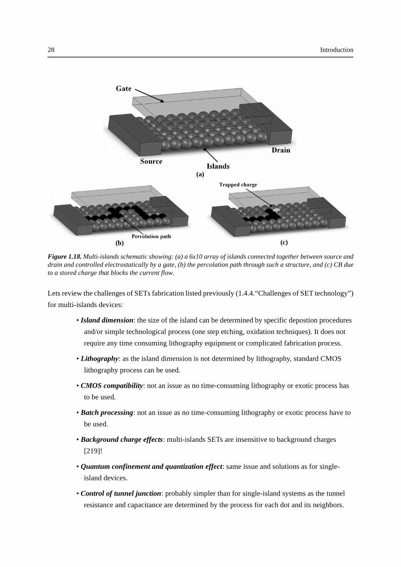
28 Introduction
Figure 1.18. Multi-islands schematic showing: (a) a 6x10 array of islands connected together between source anddrain and controlled electrostatically by a gate, (b) the percolation path through such a structure, and (c) CB dueto a stored charge that blocks the current flow.
Lets review the challenges of SETs fabrication listed previously (1.4.4.“Challenges of SET technology”)
for multi-islands devices:
• Island dimension: the size of the island can be determined by specific depostion procedures
and/or simple technological process (one step etching, oxidation techniques). It does not
require any time consuming lithography equipment or complicated fabrication process.
• Lithography: as the island dimension is not determined by lithography, standard CMOS
lithography process can be used.
• CMOS compatibility: not an issue as no time-consuming lithography or exotic process has
to be used.
• Batch processing: not an issue as no time-consuming lithography or exotic process have to
be used.
• Background charge effects: multi-islands SETs are insensitive to background charges
[219]!
• Quantum confinement and quantization effect: same issue and solutions as for single-
island devices.
• Control of tunnel junction: probably simpler than for single-island systems as the tunnel
resistance and capacitance are determined by the process for each dot and its neighbors.
(a)
(b) (c)
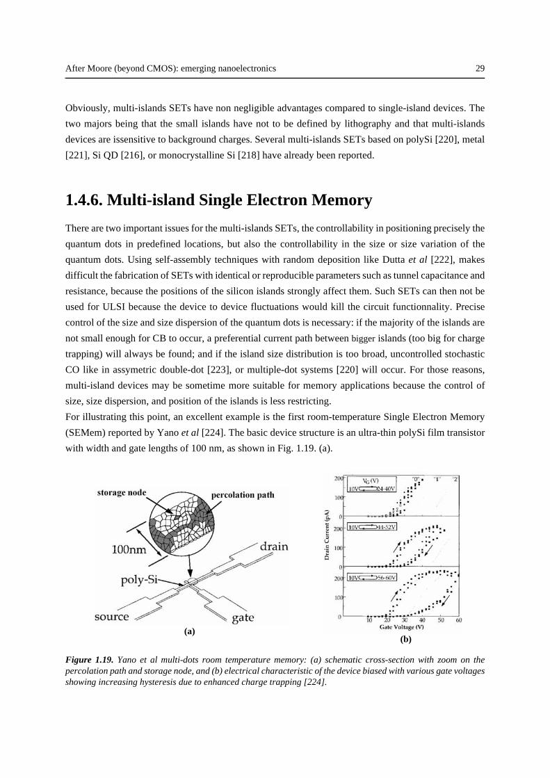
After Moore (beyond CMOS): emerging nanoelectronics 29
Obviously, multi-islands SETs have non negligible advantages compared to single-island devices. The
two majors being that the small islands have not to be defined by lithography and that multi-islands
devices are issensitive to background charges. Several multi-islands SETs based on polySi [220], metal
[221], Si QD [216], or monocrystalline Si [218] have already been reported.
1.4.6. Multi-island Single Electron Memory
There are two important issues for the multi-islands SETs, the controllability in positioning precisely the
quantum dots in predefined locations, but also the controllability in the size or size variation of the
quantum dots. Using self-assembly techniques with random deposition like Dutta et al [222], makes
difficult the fabrication of SETs with identical or reproducible parameters such as tunnel capacitance and
resistance, because the positions of the silicon islands strongly affect them. Such SETs can then not be
used for ULSI because the device to device fluctuations would kill the circuit functionnality. Precise
control of the size and size dispersion of the quantum dots is necessary: if the majority of the islands are
not small enough for CB to occur, a preferential current path between bigger islands (too big for charge
trapping) will always be found; and if the island size distribution is too broad, uncontrolled stochastic
CO like in assymetric double-dot [223], or multiple-dot systems [220] will occur. For those reasons,
multi-island devices may be sometime more suitable for memory applications because the control of
size, size dispersion, and position of the islands is less restricting.
For illustrating this point, an excellent example is the first room-temperature Single Electron Memory
(SEMem) reported by Yano et al [224]. The basic device structure is an ultra-thin polySi film transistor
with width and gate lengths of 100 nm, as shown in Fig. 1.19. (a).
Figure 1.19. Yano et al multi-dots room temperature memory: (a) schematic cross-section with zoom on thepercolation path and storage node, and (b) electrical characteristic of the device biased with various gate voltagesshowing increasing hysteresis due to enhanced charge trapping [224].
(b)(a)
30 Introduction
The poly-Si channel is as thin as 3.4 nm on average, but the film thickness varies from one position to
another, ranging from 1 to 5 nm, which is important for electron transport. The gate oxide is 150nm thick,
reducing capacitance between the gate and the channel. The drain current is measured as the gate voltage
is swept up and down between 10V and VGmax (>10V), the maximum gate voltage, as shown in Fig.
1.19. (b). When VGmax is less than 40V, the current is almost independent of the sweeping direction.
However, suddenly, when the maximum gate voltage is 44V, clear hysteresis is observed. The threshold
shifts by about 10V. A similar second threshold jump is observed at about 56V. It is confirmed that the
individual carrier trapping in the fabricated channel (storage node on Fig. 1.19. (a)) causes the hysteresis,
and the associated memory effect is very stable, lasting more than 1 hour, which makes it suitable for
memory applications.
1.5. Summary
In this chapter, we have first recalled CMOS evolution driven by scaling and cost over the last fourty
years. The agressive scaling of CMOS has lead to transistor limitations that have been detailled in terms
of gate oxide thickness, poly gate depletion, parasitic resistances, SCE, DIBL channel doping control,
and lithography. We have then described the "more Moore" orientation of research that should allow to
extend CMOS till the 16nm node in 2019. Leading manufacturers, but also academic communities are
pursuing two avenues to meet these "more Moore" challenges: (i) evolutionary CMOS that addresses
nanoscale challenges by new materials and device engineering, and (ii) non-classical CMOS which
includes multi-gate devices, UTB SOI and vertical transistors. This results in alternative single-gate
nonclassical MOSFETs devices using innovative materials like high-k dielectrics, metal gates and/or
strained silicon, but also alternative multiple-gate nonclassical MOSFET devices with innovative
architectures like double, triple gate and/or vertical MOSFETS. A possible path to reach the 16nm is
finally proposed.
In the second part of the detailled discussion of CMOS future evolution, we have focused on the beyond
CMOS ("after Moore") orientation of research. Indeed, beyond the 16nm node, the semiconductor
industry will have to find fundamentaly new approaches to information, signal processing, and data-
storage, which implies the exploitation of alternative devices, materials, and process, but also involves
systems innovations. The discussion has been deliberately limited to the most promising emerging logic
devices, as defined by the 2005 ITRS. A stronger emphasis has been put on 1D structures. SE devices
are also described in more detail because of their higher relevance for this work. Finally, we have
highlighted the SET fabrication challenges and introduced the concept of multi-island devices as an
interesting alternative to lithoraphically defined SETs or SEMems.

Summary 31
Considering the challenges of "more Moore" and "after Moore" research in nanoelectronics, we have
decided to focus our work on polysilicon nanowire transistors that can be used either in logic, memory,
SET, SEMem, or hybrid CMOS-"nano" applications. Polysilicon nanowires also combine the
advantages of both 1D structures and multi-islands devices, in which the main device is lithographically
defined but the intrinsic properties depends on the nanomaterial features. Finally, as it will be described
in the next chapter, polysilicon is a low-cost, and relatively easy to handle material.

32 Introduction
References 33
1.6. References
[1] G. E. Moore, "Cramming more components onto integrated circuits", Electronics, vol. 38, no. 8, April 1965.
[2] Available online at http://www.bellsystemmemorial.com/belllabs_transistor.html
[3] S. Augarten, "State of the art: a photographic history of the integrated circuit", Ticknor & Fields, NewHaven and New York, 1983.
[4] G. E. Moore, "Progress in Digital Integrated Electronics", Technical Digest of the International ElectronDevices Meeting IEDM 1975, pp. 11-13, 1975.
[5] G. E. Moore, "Lithography and the Future of Moore’s Law", Proceedings of SPIE, vol. 2437, May 1995.
[6] Available online at http://www.intel.com/pressroom/archive/speeches/gem93097.htm .
[7] G. E. Moore, "No exponential is Forever: But "Forever" Can Be Delayed!", International Solid-StateCircuits Conference ISSCC 2003 Digest of Technical Papers, vol. 1, pp. 20-23, 2003.
[8] Available online at http://www.intel.com/pressroom/archive/releases/20060718comp.htm.
[9] Available online at http://www.intel.com/technology/silicon/mooreslaw/index.htm .
[10] SIA: International Technology Roadmap for Semiconductors (ITRS), 2005 Edition, available online: http://public.itrs.net/.
[11] D. A. Muller, T. Sorsch, S. Moccio, F. H. Baumann, K. Evans-Lutterodt, and G. Timp, "The electronicstructure at the atomic scale of ultrathin gate oxides", Nature, vol. 399, pp. 758-761, 1999.
[12] B. Yu, H. Wang, C. Riccobene, Q. Xiang, and M.-R. Lin, "Limits of Gate-Oxide Scaling in Nano-Transistors", Symposium on VLSI Technology 2000 Digest of Technical Papers, pp. 90-91, 2000.
[13] M. S. Krishnan, L. Chang, T.-J. King, J. Bokor, and C. Hu, "MOSFETs with 9 to 13A Thick Gate Oxides",Technical Digest of the International Electron Devices Meeting IEDM 1999, pp. 241-243, 1999.
[14] S.-I. Takagi, M. Takayanagi, and A. Toriumi, "Experimental Examination of Physical Model for DirectTunneling Current in Unstressed/Stressed Ultrathin Gate Oxides", Technical Digest of the InternationalElectron Devices Meeting IEDM 1999, pp. 461-464, 1999.
[15] M. Koh, W. Mizubayashi, K. Iwamoto, H. Murakami, T. Ono, M. Tsuno, T. Mihara, K. Shibahara, S.Miyazaki, and M. Hirose, "Limit of Gate Oxide Thickness Scaling in MOSFETs due to Apparent ThresholdVoltage Fluctuation Induced by Tunnel Leakage Current", IEEE Transactions on Electron Devices, vol. 48(2), pp. 259-264, 2001.
[16] T. D. Plummer, and P. B. Griffin, "Material and Process Limits in Silicon VLSI Technology", Proceedingsof the IEEE, vol. 89 (3), pp. 240-258, 2001.
[17] Y. Taur, C. H. Wann, and D. J. Frank, "25nm CMOS Design Considerations", Technical Digest of theInternational Electron Devices Meeting IEDM 1998, pp. 789-792, 1998.
[18] R. H. Dennard, F. H. Gaensslen, H.-N. Yu, V. Leorideout, E. Bassous, and A. R. Leblanc, "Design of Ion-Implanted MOSFET’s with Very Small Physical Dimensions", IEEE Journal of Solid-State Circuits, vol. 9(5), pp. 256-268, 1974.
[19] S.-D. Kim, C.-M. Park, and J. C. S. Woo, "Advanced Model and Analysis of Series Resistance for CMOSSclaing Into Nanometer Regime - Part II: Quantitative Analysis", IEEE Transactions on Electron Devices,vol. 49 (3), pp. 467-472, 2002.
[20] S. E. Thompson, and S. Parthasarathy, "Moore’s law: the future of Si microelectronics", Materials Today,vol. 9 (6), pp. 20-25, 2006.
[21] S. Deleonibus, C. Caillat, G. Guegan, M. Heitzmann, M. E. Nier, S. Tedesco, B. Dal’zotto, F. Martin, P.Mur, A. M. Papon, G. Lecarval, S. Biswas, and D. Souil, "A 20-nm Physical Gate Length NMOSFETFeaturing 1.2nm Gate Oxide, Shallow Implanted Source and Drain and BF2 Pockets", IEEE ElectronDevice Letters, vol. 21 (4), pp. 173-175, 2000.
[22] Y. Taur, "CMOS design near the limit of scaling", IBM Journal of Research and Development, vol. 46 (2/3), pp. 213-222, 2002.
[23] Y. Taur, and E. J. Nowak, "CMOS Devices below 0.1µm: How High Will Performance Go?", TechnicalDigest of the International Electron Devices Meeting IEDM 1997, pp. 215-218, 1997.
34 Introduction
[24] D. J. Frank, R. H. Dennard, E. Nowak, P. M. Solomon, Y. Taur, and H.-S. P. Wong, "Device Scaling Limitsof Si MOSFETs and Their Application Dependencies", Proceedings of the IEEE, vol. 89 (3), pp. 259-287,2001.
[25] T. Skotnicki, "Heading for decananometer CMOS - Is navigation among icebergs still a viable strategy?",Proceedings of ESSDERC 2000, pp. 19-33, 2000.
[26] T. Mizuno, J. Okamura, and A. Toriumi, "Experimental study of threshold voltage fluctuation due tostastistical variation of channel dopant number in MOSFETs", IEEE Transactions on Electron Devices, vol.41 (11), pp. 2216-2221, 1994.
[27] S. Asai, and Y. Wada, "Technology Challenges for Integration Near and Below 0.1µm", Proceedings of theIEEE, vol. 85 (4), pp. 505-520, 1997.
[28] A. Asenov, A. R. Brown, J. H. Davies, S. Kaya, and G. Slavcheva, "Simulation of Intrinsic ParameterFluctuations in Decananometer and Nanometer-Scale MOSFETS", IEEE Transactions on ElectronDevices, vol. 50 (9), pp. 1837-1852, 2003.
[29] L. R. Harriott, "Limits of Lithography", Proceedings of the IEEE, vol. 89 (3), pp. 366-374, 2001.
[30] B. J. Lin, "Lithography for maufacturing of sub-65nm nodes and beyond", Proceedings of the IEEE, 2005.
[31] H.-S. P. Wong, "Silicon Devices at the «End of Sclaing» - Opportunities and Challenges", available online:http://www.stanford.edu/hspwong, 2005.
[32] T. Mizuno, N. Sugiyama, T. Tezuka, T. Numata, and S. Takagi, "High Performance CMOS Operation ofStrained-SOI MOSFETs using Thin Film SiGe-on-Insulator Substrate", Symposium on VLSI Technology2002 Digest of Technical Papers, pp. 106-107, 2002.
[33] T. Tezuka, N. Sugiyama, T. Mizuno, and S. Takagi, "High-performance Strained Si-on-Insulator MOSFETsby Novel Fabrication Processes Utilizing Ge-Condensation Technique", Symposium on VLSI Technology2002 Digest of Technical Papers, pp. 96-97, 2002.
[34] N. Collaert, P. Verheyen, K. D. Meyer, R. Loo, and M Caymax, "High-Performance Strained Si/SiGepMOS Devices With Multiple Quantum Wells", IEEE Transactions on Nanotechnology, vol. 1 (4), pp. 190-194, 2002.
[35] M. L. Lee, C. W. Leitz, Z. Cheng, A. J. Pitera, T. Langdo, M. T. Currie, G. Taraschi, E. A. Fitzgerald, andD. A. Antoniadis, "Strained Ge channel p-type metal-oxide-semiconductor field-effect transistors grown onSi1-xGex/Si virtual substrates", Applied Physics Letters, vol. 79 (20), pp. 3344-3346, 2001.
[36] C. W. Leitz, M. T. Currie, M. L. Lee, Z. Cheng, D. A. Antoniadis, and E. A. Fitzgerald, "Hole mobilityenhancements in strained Si/Si1-yGey p-type metal-oxide-semiconductor field-effect transistors grown onrelaxed Si1-xGex/Si (x<y) virtual substrates", Applied Physics Letters, vol. 79 (25), pp. 4246-4248, 2001.
[37] L. Huang, J. O. Chu, S. A. Goma, C. P. D’Emic, S. J. Koester, D. F. Canaperi, P. M. Mooney, S. A. Cordes,J. L. Speidell, R. M. Anderson, and H.-S. P. Wong, "Electron and Hole Mobility Enhancement in StrainedSOI by Wafer Bonding", IEEE Transactions on Electron Devices, vol. 49 (9), pp. 1566-1571, 2002.
[38] J. R. Hwang, J. H. Ho, S. M. Ting, T. P. Chen, Y. S. Hsieh, C. C. Huang, Y. Y. Chaing, H. K. Lee, A. Liu,T. M. Shen, G. Braithwaite, M. Currie, N. errish, R. Hammond, A. Lochtefeld, F. Singaporewala, M.Bulsara, Q. Xiang, M. R. Lin, W. T. Shiau, Y. T. Loh, J. k. Chen, S. C. Chien, and F. Wen, "Performanceof 70nm Strained-Silicon CMOS Devices", Symposium on VLSI Technology 2003 Digest of TechnicalPapers, pp. 103-105, 2003.
[39] K. Rim, J. Chu, H. Chen, K. A. Jenkins, T. Kanarsky, K. Lee, A. Mocuta, H. Zhu, R. Roy, J. Newbury, J.Ott, K. Petrarca, P. Mooney, D. Lacey, S. Koester, K. Chan, D. Boyd, M. Ieong, and H.-S. P. Wong,"Characteristics and Device Design of Sub-100nm Strained Si N- and PMOSFETs", Symposium on VLSITechnology 2002 Digest of Technical Papers, pp. 98-99, 2002.
[40] S. E. Thompson, M. Armstrong, C. Auth, S. Cea, R. Chau, G. Glass, T. Hoffman, J. Klaus, Z. Ma, B.Mcintyre, A. Murthy, B. Obradovic, L. Shifren, S. Sivakumar, S. Tyagi, T. Ghani, K. Mistry, Mark Bohr,and Y. El-Mansy, "A Logic Nanotechnology Featuring Strained-Silicon", IEEE Electron Device Letters,vol. 25 (4), pp. 191-193, 2004.
[41] K. Mistry, M. Armstrong, C. Auth, S. Cea, T. Coan, T. Ghani, T. Hoffmann, A. Murthy, J. Stanford, R.Shaheed, K. Zawadzki, K. Zhang, S. Thompson, and M. Bohr, "Delaying Forever: UNiaxial StrainedSilicon Transistors in a 90nm CMOS Technology", Symposium on VLSI Technology 2004 Digest ofTechnical Papers, pp. 50-51, 2004.
[42] P. Bai, C. Auth, S. Balakrishnan, M. Bost, R. Brain, V. Chikarmane, R. Heussner, M. Hussein, J. Hwang,D. Ingerly, R. James, J. Jeong, C. Kenyon, E. Lee, S.-h. Lee, N. Lindert, M. Liu, Z. Ma, T. Marieb, A.Murthy, R. Nagisetty, S. Natarajan, J. Neirynck, A. Ott, C. Parker, J. Sebastian, R. Shaheed, S. Sivakumar,
References 35
J. Steigerwald, S. Tyagi, C. Weber, B. Woolery, A. Yeoh, K. Zhang, and M. Bohr " A 65nm LogicTechnology Featuring 35nm Gate Lengths, Enhanced Channel Strain, 8 Cu Interconnect Layers, Low-kILD and 0.57 µm2 SRAM cell", Technical Digest of the International Electron Devices Meeting IEDM2004, pp. 657-660, 2004.
[43] H. Ohta, Y. Kim, Y. Shimamune, T. Sakuma, A. Hatada, A. Katakami, T. Soeda, K. Kawamura, H. Kokura,H. Morioka, T. Watanabe, J. Oh, Y. Hayami, J. Ogura, M. Tajima, T. Mori, N. Tamura, M. Kolima, and K.Hashimoto, "High Performance 30nm Gate Bulk CMOS for 45nm Node with Σ-shaped SiGe-SD",Technical Digest of the International Electron Devices Meeting IEDM 2005, pp. 237-240, 2005.
[44] A. Oishi, O. Fujii, T. Yokoyama, K. Ota, T. Sanuki, H. Inkuma, K. Eda, T. Idaka, H. Miyajima, S. Iwasa,H. Yamasaki, K. Oouchi, K. Matsuo, H. Nagano, T. Komoda, Y. Okayama, T. Matsumoto, K. Fukasaku,T. Shimizu, K. Miyano, T. Suzuki, K. Yahashi, A. Horiuchi, Y. Takegawa, K. Saki, S. Mori, K. Ohno, I.Mizushima, M. Saito, M. Iwai, S. Yamada, N. Nagashima, and F. Matsuoka, "High PerformanceCMOSFET Technology for 45nm Generation and Scalability of Stress-Induced Mobility EnhancementTechnique", Technical Digest of the International Electron Devices Meeting IEDM 2005, pp. 229-232,2005.
[45] K. Rim, K. Chan, L. Shi, D. Boyd, J. Ott, N. Klymko, F. Cardone, L. Tai, S. Koester, M. Cobb, D. Canaperi,B. To, E. Duch, I. Babich, R. Carruthers, P. Saunders, G. Walker, Y. Zhang, M. Steen, And M. Ieong,"Fabrication and Mobility Characteristics of Ultra-thin Strained Si Directly on Insulator (SSDOI)MOSFETs", Technical Digest of the International Electron Devices Meeting IEDM 2003, pp. 59-52, 2003.
[46] T. Tezuka, N. Sugiyama, T. Mizuno, and S. Takagi, "Ultrathin Body SiGE-on-Insulator pMOSFETs WithHigh-Mobility SiGe Surface Channels", IEEE Transactions on Electron Devices, vol. 50 (5), pp. 1328-1333, 2003.
[47] M. Yang, M. Ieong, L. Shi, K. Chan, V. Chan, A. Chou, E. Gusev, K. Jenkins, D. Boyd, Y. Ninomiya, D.Pendleton, Y. Surpris, D. Heenan, J. Ott, K. Guarini, C. D’Emic, M. Cobb, P. Mooney, B. To, N. Rovedo,J. Benedict, R. Mo, and H. Ng, "High Performance CMOS Fabricated on Hybrid Substrate With DifferentCrystal Orientations", Technical Digest of the International Electron Devices Meeting IEDM 2003, pp. 453-456, 2003.
[48] M. Iwai, A. Oishi, T. Sanuki, Y. Takegawa, T. Komoda, Y. Morimasa, K. Ishimura, M. Takayanagi, K.Eguchi, D. Matsushita, K. Muraoka, K. Sunouchi, and T. Noguchi, "45nm CMOS Platform Technology(CMOS6) with High Density Embedded Memories", Symposium on VLSI Technology 2004 Digest ofTechnical Papers, pp. 12-13, 2004.
[49] F. Boeuf, F. Arnaud, C. Boccaccio, F. Salvetti, J. Todeschini, L. Pain, M. Jurdit, S. Manakli, B. Icard, N.Planes, N. Gierczynski, S. Denorme, B. Borot, C. Ortolland, B. Duriez, B. Tavel, P. Gouraud, M. Broekaart,V. Dejonghe, P. Brun, F. Guyader, P. Morin, C. Reddy, M. Aminpur, C. Laviron, S. Smith, J. P. Jacquemin,M. Mellier, F. André, N. Bicais-Lepinais, S. Jullian, J. Bustos, and T. Skotnicki, "0.248µm2 and 0.334µm2
Conventional Bulk 6T_SRAM bit-cells for 45nm node Low Cost-General Purpose Applications",Symposium on VLSI Technology 2005 Digest of Technical Papers, pp. 130-131, 2005.
[50] Technical Digest of the International Electron Devices Meeting IEDM 2005, Session 2, Session 17, andSession 36, 2005.
[51] Y. Zheng, H. Mizuta, Y. Tsuchiya, M. Endo, D. Sato, and S. Oda, "In situ real-time spectroscopicellipsometry study of HfO2 thin films grown by using the pulsed-source metal-organic chemical-vapordeposition", Journal of Applied Physics , 2005.
[52] T. Hayashi, M. Mizutani, M. Inoue, J. Yugami, J. Tsuchimoto, M. Anma, S. Komori, K. Tsukamoto, Y,Tsukamoto, K. Nii, Y. Nishida, H. Sayama, T. Yamashita, H. Oda, T. Eimori, and Y. Ohji, "Vth-tunableCMIS Platform with High-k gate Dielectrics and Variability Effect for 45nm node", Technical Digest of theInternational Electron Devices Meeting IEDM 2005, pp. 906-909, 2005.
[53] S. Datta, G. Dewey, M. Doczy, B. S. Doyle, B. Jin, J. Kavalieros, R. Kotlyar, M. Metz, N. Zelick, and R.Chau, "High Mobility Si/SiGe Strained Channel MOS Transistors with HfO2/TiN Gate Stack", TechnicalDigest of the International Electron Devices Meeting IEDM 2003, pp. 653-656, 2003.
[54] P. Verheyen, G. Enemann, R. Rooyackers, R. Loo, L. Eeckhout, D. Rondas, F. Leys, J. Snow, D.Shamiryan, M. Demand, Th. Y. Hoffman, M. Goodwin, H. Fujimoto, C. Ravit, B-C. Lee, M. Caymax, K.De Meyer, P. Absil, M. Jurczak, and S. Biesemans, "Demonstration of Recessed SiGe S/D and InsertedMetal Gate on HfO2 for High Performance pFETs", Technical Digest of the International Electron DevicesMeeting IEDM 2005, pp. 886-889, 2005.
[55] M. A. Quevedo-Lopez, S. A. Krishnan, P. D. Kirsch, H. J. Li, J. H. Sim, C. Huffman, J. J. Peterson, B. H.Lee, G. Pant, B. E. Gnade, M. J. Kim, R. M. Wallace, D. Guo, H. Bu, and T. P. Ma, "High PerformanceGate First HfSiON Dielectric Satisfying 45nm Node Requirements", Technical Digest of the International
36 Introduction
Electron Devices Meeting IEDM 2005, pp. 425-428, 2005.
[56] X. Yu, C. Zhu, M. Yu, M. F. Li, A. Chin, C. H. Tung, D. Gui, and D.-L. Kwong, "Advanced MOSFETsUsing HfTaON/SiO2 Gate Dielectric and TaN Metal Gate with Excellent Performances for Low StandbyPower Application", Technical Digest of the International Electron Devices Meeting IEDM 2005, pp. 27-30, 2005.
[57] R. I. Hegde, D. H. Triyoso, P. J. Tobin, S. Kalpat, M. E. Ramon, H.-H. Tseng, J. K. Schaeffer, E.Luckowski, W. J. Taylor, C. C. Capasso, D. C. Gilmer, M. Moosa, A. Haggag, M. Raymond, D. Roan, J.Nguyen, L. B. La, E. Hebert, R. Cotton, X-D. Wang, S. Zollner, R. Gregory, D. Werho, R. S. Rai, L.Fonseca, M. Stoker, C. Tracy, B. W. Chan, Y. H. Chiu, and B. E. White Jr., "Microstructure Modified HfO2Using Zr with TaxCy Gate for Improved Device Performance and Reliability", Technical Digest of theInternational Electron Devices Meeting IEDM 2005, pp. 35-38, 2005.
[58] C. O. Chui, H. Kim, D. Chi, B. B. Triplett, P. C. McIntyre, and K. C. Saraswat, "A Sub-400°C GermaniumMOSFET Technology with High-k Dielectric and Metal Gate", Technical Digest of the InternationalElectron Devices Meeting IEDM 2002, pp. 437-440, 2002.
[59] Y. Kamata, Y. Kamimuta, T. Ino, R. Iijima, M. Koyama, and A. Nishiyama, "Dramatic Improvement ofGe p-MOSFET Characteristics Realized by Amorphous Zr-Silicate/Ge Gate Stack with Excellent StructuralStability through Process Temperatures", Technical Digest of the International Electron Devices MeetingIEDM 2005, pp. 429-432, 2005.
[60] M. Suzuki, M. Tomita, T. Yamaguchi, and N. Fukushima, "Ultra-thin (EOT=3A) and low leakagedielectrics of La-alminate directly on Si substrate fabricated by high temperature deposition", TechnicalDigest of the International Electron Devices Meeting IEDM 2005, pp. 433-436, 2005.
[61] Y. T. Hou, F. Y. Yen, P. F. Hsu, V. S. Chang, P. S. Lim, C. L. Hung, L. G. Yao, J. C. Jiang, H. J. Lin, Y.Jin, S. M. Jang, H. J. Tao, S. C. Chen, and M. S. Liang, "High Performance Tantalum Carbide Metal GateStacks for nMOSFET Application", Technical Digest of the International Electron Devices Meeting IEDM2005, pp. 31-34, 2005.
[62] T. Hirano, T. Ando, K. Tai, S. Yamaguchi, T. Kato, S. Hiyama, Y. Hagimoto, S. Takesako, N. Yamagishi,K. Watanabe, R. Yamamoto, S. Kanda, S. Terauchi, Y. Tateshita, Y. Tagawa, H. Iwamoto, M. Saito, S.Kadomura, and N. Nagashima, "High Performance nMOSFET with HfSix/HfO2 Gate Stack by LowTemperature Process", Technical Digest of the International Electron Devices Meeting IEDM 2005, pp.890-892, 2005.
[63] S. Inumiya, Y. Akasaka, T. Matsuki, F. Ootsuka, K. Torii, and Y. Nara, "A Thermally-Stable Sub-0.9nmEOT TaSix/HfSiON Gate Stack with High Electron Mobility, Suitable for Gate-First Fabrication of hp45LOP Devices", Technical Digest of the International Electron Devices Meeting IEDM 2005, pp. 23-26,2005.
[64] M. Müller, A. Mondot, N. Gierczynski, D. Aimé, B. Froment, F. Leverd, P. Gouraud, A. Talbot, S.Descombes, Y. Morand, Y. Le Tiec, P. Besson, A. Toffoli, G. Ribes, J.-M. Roux, S. Pokrant, F. And5ré,and T. Skotnicki, "An easily integrable NiSi TOSI-gate-gate/SiON-module for LP SRAM applicationsbased on a single step silicidation of gate and junction", Technical Digest of the International ElectronDevices Meeting IEDM 2005, pp. 626-629, 2005.
[65] A. Lauwers, A. Veloso, T. Hoffmann, M. J. H. van Dal, C. Vrancken, S. Brus, S. Locorotondo, J.-F. deMarneffe, B. Sijmus, S. Kubicek, T. Chiarella, M. A. Pawlak, K. Opsomer, M. Niwa, R. Mitsuhashi, K. G.Anil, H. Y. Yu, C. Demeurisse, R. Verbeeck, M. de Potter, P. Absil, K. Maex, M. Jurczak, S. Biesemans,and J. A. Kittl, "CMOS Integration of Dual Work Function Phase Controlled Ni FUSI with SimultaneousSilicidation of NMOS (NiSi) and PMOS (Ni-rich silicide) Gates on HfSiON", Technical Digest of theInternational Electron Devices Meeting IEDM 2005, pp. 646-649, 2005.
[66] H. Y. Yu, J. D. Chen, M. F. Li, S. J. Lee, D. L. Kwong, M. van Dal, J. A. Kittl, A. Lauwers, E. Augendre,S. Kubicek, C. Zhao, H. Bender, B. Brijs, L. Geenen, A. Benedetti, P. Absil, M. Jurczak, and S. Biesemans,"Moduation of the Ni FUSI workfunction by Yb doping: from midgap to n-type band-edge", TechnicalDigest of the International Electron Devices Meeting IEDM 2005, pp. 630-633, 2005.
[67] H. Y. Yu, R. Singanamalla, K. Opsomer, E. Augendre, E. Simoen, J. A. Kittl, S. Kubicek, S. Severi, X. P.Shi, S. Brus, C. Zhao, J. F. Marneffe, S. Locorotondo, D. Shamiryan, M. van Dal, A. Veloso, A. Lauwers,M. Niwa, K. Maex, K. D. Meyer, P. Absil, M. Jurczak, and S. Biesemans, "Demonstration of Ni FullyGermanoSilicide as a pFET Gate Electrode Candidate on HfSiON", Technical Digest of the InternationalElectron Devices Meeting IEDM 2005, pp. 638-641, 2005.
[68] D. S. Yu, A. Chin, C. H. Wu, M.-F. Li, C. Zhu, S. J. Wang, W. J. Yoo, B. F. Hung, and S. P. McAlister,"Lanthanide and Ir-based Dual Metal-Gate/HfAlON CMOS with Large Work-Function Difference",Technical Digest of the International Electron Devices Meeting IEDM 2005, pp. 634-637, 2005.
References 37
[69] N. Biswas, S. Novak, B. Chen, D. Lichtenwalner, M Ozturk, and V. Misra, "NixTa1-xSi and NixPt1-xSiTernary Alloys for Work function Tuning on SiO2, HfSiOx and HfO2 Dielectrics", Technical Digest of theInternational Electron Devices Meeting IEDM 2005, pp. 650-653, 2005.
[70] SIA: International Technology Roadmap for Semiconductors (ITRS), 2004 Update, available online: http://public.itrs.net/.
[71] W.-Y. Lu, and Y. Taur, "On the Scaling Limit of Ultrathin SOI MOSFETs", IEEE Transactions on ElectronDevices, vol. 53 (5), pp. 1137-1141, 2006.
[72] B. Doris, M. Ieong, T. Kanarsky, Y. Zhang, R. A. Roy, O. Dokumaci, Z. Ren, F.-F. Jamin, L. Shi, W. Natzle,H.-J. Huang, J. Mezzapelle, A. Mocuta, S. Womack, M. Gribelyuk, E. C. Jones, R. J. Miller, H.-S. P. Wong,and W. Haensch, "Extreme scaling with Ultra-Thin Si Channel MOSFETs", Technical Digest of theInternational Electron Devices Meeting IEDM 2002, pp. 267-270, 2002.
[73] B. Doris, M. Ieong, H. Zhu, Y. Zhang, M. Steen, W. Natzle, S. Callegari, V. Narayanan, J. Cai, S. H. Ku,P. Jamison, Y. Li, Z. Ren, V. Ku, D. Boyd, T. Kanarsky, C. D’Emic, M. Newport, D. Dobuzinsky, S.Deshpande, J. Petrus, R. Jammy, and W. Haensch, "Device Design Considerations for Ultra-Thin SOIMOSFETs", Technical Digest of the International Electron Devices Meeting IEDM 2003, pp. 631-634,2003.
[74] E. Suzuki, K. Ishii, S. Kanemura, T. Maeda, T. Toshiyuki, T. Sekigawa, K. Nagai, and H. Hiroshima,"Highly Suppressed Short-Channel Effects in Ultrathin SOI n-MOSFET’s", IEEE Transactions on ElectronDevices, vol. 47 (2), pp. 354-359, 2000.
[75] K. Uchida, H. Watanabe, A. Kinoshita, J. Koga, T. Numata, and S. Takagi, "Experimental Study on CarrierTransport Mechanism in Ultrathin-body SOI n- and p-MOSFETS with SOI Thickness less than 5nm",Technical Digest of the International Electron Devices Meeting IEDM 2002, pp. 47-50, 2002.
[76] M. Jurczak, T. Skotnicki, M. Paoli, B. Tormen, J. Martins, J. L. Regolini, D. Dutartre, P. Ribot, D. Lenoble,R. Pantel, and S. Monfray, "Silicon-on-Nothing (SON) - an Innovative Process for Advanced CMOS",IEEE Transactions on Electron Devices, vol. 47 (11), pp. 2179-2187, 2000.
[77] J. Pretet, S. Monfray, S. Cristoloveanu, and T. Skotnicki, "Silicon-on-Nothing MOSFETs: Performance,Short-Channel Effects, and Backgate Coupling", IEEE Transactions on Electron Devices, vol. 51 (2), pp.240-245, 2004.
[78] T. Sato, H. Nii, M. Hatano, K. takenaka, H. Hayashi, K. Ishigo, T. Hirano, K. Ida, N. Aoki, T. Ohguro, K.Ino, I. Mizushima, and Y. Tsunashima, "SON (Silicon on Nothing) MOSFET using ESS (Empty Space inSilicon) technique for SoC applications", Technical Digest of the International Electron Devices MeetingIEDM 2001, pp. 809-812, 2001.
[79] Y. Tian, R. Huang, X. Zhang, and Y. Wang, "A Novel Nanoscaled Device Concept: Quasi-SOI MOSFETto Eliminate the Potential Weaknesses of UTB SOI MOSFET", IEEE Transactions on Electron Devices,vol. 52 (4), pp. 561-568, 2005.
[80] R. Huang, Y. Tian, H. Xiao, W. Bu, C. Feng, M. Chan, X. Zhang, and Y. Wang, "Novel Localized-SOIMOSFET’s Combining the Advantages of SOI and Bulk Substrates for Highly-Scaled Devices", IEEEConference on Electron Devices and Solid-State Circuits EDSSC 2005, pp. 81-86, 2005.
[81] S. Zhu, H. Y. Yu, S. J. Whang, J. H. Chen, C. Shen, C. Zhu, S. J. Lee, M. F. Li, D. S. H. Chan, W. J. Yoo,A. Du, C. H. Tung, J. Singh, A. Chin, and D. L. Kwong, "Schottky-Barrier S/D MOSFETs With Hig-K GateDielectrics and Metal-Gate Electrode", IEEE Electron Device Letters, vol. 25 (5), pp. 268-270, 2004.
[82] M. Ieong, P. M. Solomon, S. E. Laux, H.-S. P. Wong, and D. Chidambarrao, "Comparison of Raised andSchottky Source/Drain MOSFETs Using a Novel Tunneling Contact Model", Technical Digest of theInternational Electron Devices Meeting IEDM 1998, pp. 733-736, 1998.
[83] J. Kedzierski, M. Ieong, P. Xuan, J. Bokor, T.-J. King, and C. Hu, "Design analysis of thin-body silicidesource/drain devices", IEEE International SOI Conference 2001, pp. 21-22, 2001.
[84] M. Fritze, C. L. Chen, S. Calawa, D. Yost, B. Wheeler, P. Wyatt. C. L. Keast, J. Snyder, and J. Larson,"High-Speed Schottky-Barrier pMOSFET With fT = 280GHz", IEEE Electron Device Letters, vol. 25 (4),pp. 220-222, 2004.
[85] B.-Y. Tsui, and C.-P. Lin, "A Novel 25-nm Modified Schottky-Barrier FinFET With High Performance",IEEE Electron Device Letters, vol. 25 (6), pp. 430-432, 2004.
[86] J. Kedzierski, P. Xuan, E. H. Anderson, J. Bokor, T.-J. King, and C. Hu, "Complementary silicide source/drain thin-body MOSFETs for the 20nm gate length regime", Technical Digest of the International ElectronDevices Meeting IEDM 2000, pp. 57-60, 2000.
[87] T. Ichimori, and N. Hirashita, "Fully-Depleted SOI CMOSFETS With the Fully-Silicided Source/Drain
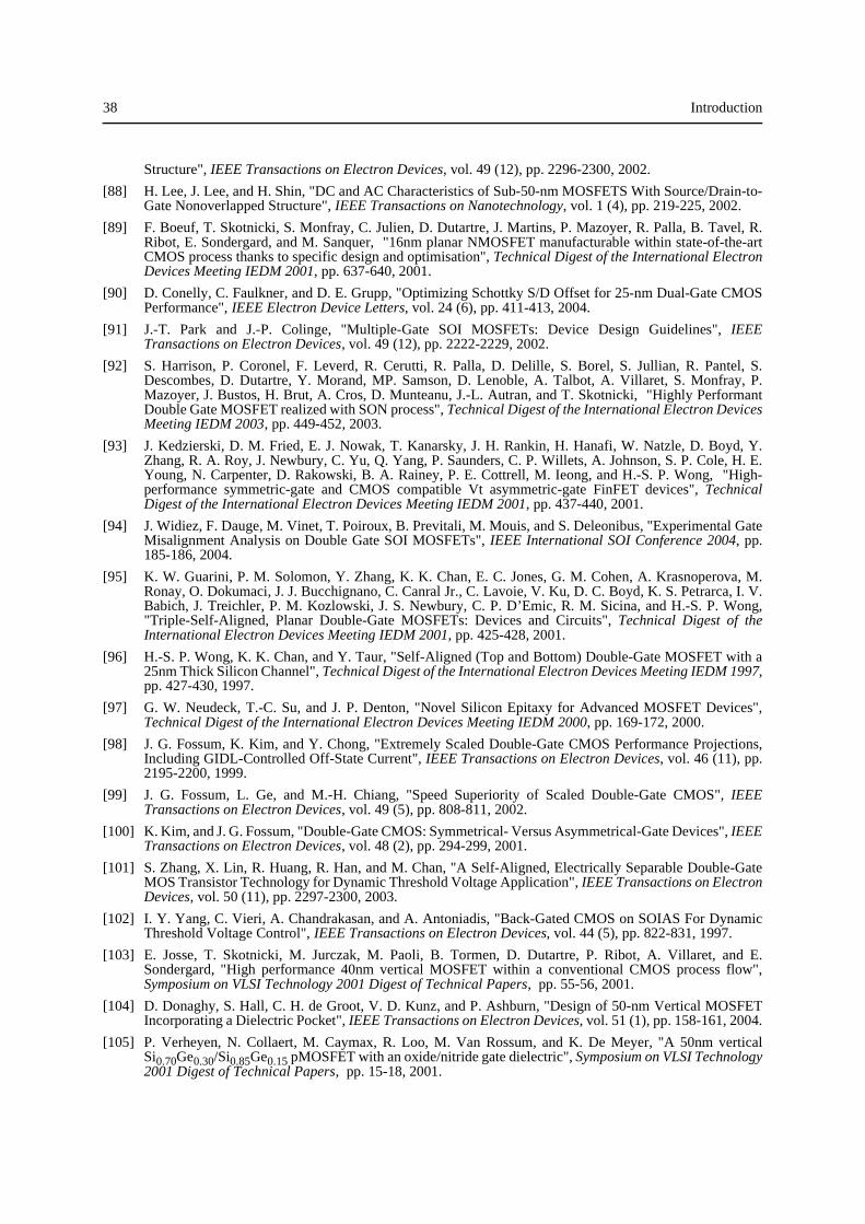
38 Introduction
Structure", IEEE Transactions on Electron Devices, vol. 49 (12), pp. 2296-2300, 2002.
[88] H. Lee, J. Lee, and H. Shin, "DC and AC Characteristics of Sub-50-nm MOSFETS With Source/Drain-to-Gate Nonoverlapped Structure", IEEE Transactions on Nanotechnology, vol. 1 (4), pp. 219-225, 2002.
[89] F. Boeuf, T. Skotnicki, S. Monfray, C. Julien, D. Dutartre, J. Martins, P. Mazoyer, R. Palla, B. Tavel, R.Ribot, E. Sondergard, and M. Sanquer, "16nm planar NMOSFET manufacturable within state-of-the-artCMOS process thanks to specific design and optimisation", Technical Digest of the International ElectronDevices Meeting IEDM 2001, pp. 637-640, 2001.
[90] D. Conelly, C. Faulkner, and D. E. Grupp, "Optimizing Schottky S/D Offset for 25-nm Dual-Gate CMOSPerformance", IEEE Electron Device Letters, vol. 24 (6), pp. 411-413, 2004.
[91] J.-T. Park and J.-P. Colinge, "Multiple-Gate SOI MOSFETs: Device Design Guidelines", IEEETransactions on Electron Devices, vol. 49 (12), pp. 2222-2229, 2002.
[92] S. Harrison, P. Coronel, F. Leverd, R. Cerutti, R. Palla, D. Delille, S. Borel, S. Jullian, R. Pantel, S.Descombes, D. Dutartre, Y. Morand, MP. Samson, D. Lenoble, A. Talbot, A. Villaret, S. Monfray, P.Mazoyer, J. Bustos, H. Brut, A. Cros, D. Munteanu, J.-L. Autran, and T. Skotnicki, "Highly PerformantDouble Gate MOSFET realized with SON process", Technical Digest of the International Electron DevicesMeeting IEDM 2003, pp. 449-452, 2003.
[93] J. Kedzierski, D. M. Fried, E. J. Nowak, T. Kanarsky, J. H. Rankin, H. Hanafi, W. Natzle, D. Boyd, Y.Zhang, R. A. Roy, J. Newbury, C. Yu, Q. Yang, P. Saunders, C. P. Willets, A. Johnson, S. P. Cole, H. E.Young, N. Carpenter, D. Rakowski, B. A. Rainey, P. E. Cottrell, M. Ieong, and H.-S. P. Wong, "High-performance symmetric-gate and CMOS compatible Vt asymmetric-gate FinFET devices", TechnicalDigest of the International Electron Devices Meeting IEDM 2001, pp. 437-440, 2001.
[94] J. Widiez, F. Dauge, M. Vinet, T. Poiroux, B. Previtali, M. Mouis, and S. Deleonibus, "Experimental GateMisalignment Analysis on Double Gate SOI MOSFETs", IEEE International SOI Conference 2004, pp.185-186, 2004.
[95] K. W. Guarini, P. M. Solomon, Y. Zhang, K. K. Chan, E. C. Jones, G. M. Cohen, A. Krasnoperova, M.Ronay, O. Dokumaci, J. J. Bucchignano, C. Canral Jr., C. Lavoie, V. Ku, D. C. Boyd, K. S. Petrarca, I. V.Babich, J. Treichler, P. M. Kozlowski, J. S. Newbury, C. P. D’Emic, R. M. Sicina, and H.-S. P. Wong,"Triple-Self-Aligned, Planar Double-Gate MOSFETs: Devices and Circuits", Technical Digest of theInternational Electron Devices Meeting IEDM 2001, pp. 425-428, 2001.
[96] H.-S. P. Wong, K. K. Chan, and Y. Taur, "Self-Aligned (Top and Bottom) Double-Gate MOSFET with a25nm Thick Silicon Channel", Technical Digest of the International Electron Devices Meeting IEDM 1997,pp. 427-430, 1997.
[97] G. W. Neudeck, T.-C. Su, and J. P. Denton, "Novel Silicon Epitaxy for Advanced MOSFET Devices",Technical Digest of the International Electron Devices Meeting IEDM 2000, pp. 169-172, 2000.
[98] J. G. Fossum, K. Kim, and Y. Chong, "Extremely Scaled Double-Gate CMOS Performance Projections,Including GIDL-Controlled Off-State Current", IEEE Transactions on Electron Devices, vol. 46 (11), pp.2195-2200, 1999.
[99] J. G. Fossum, L. Ge, and M.-H. Chiang, "Speed Superiority of Scaled Double-Gate CMOS", IEEETransactions on Electron Devices, vol. 49 (5), pp. 808-811, 2002.
[100] K. Kim, and J. G. Fossum, "Double-Gate CMOS: Symmetrical- Versus Asymmetrical-Gate Devices", IEEETransactions on Electron Devices, vol. 48 (2), pp. 294-299, 2001.
[101] S. Zhang, X. Lin, R. Huang, R. Han, and M. Chan, "A Self-Aligned, Electrically Separable Double-GateMOS Transistor Technology for Dynamic Threshold Voltage Application", IEEE Transactions on ElectronDevices, vol. 50 (11), pp. 2297-2300, 2003.
[102] I. Y. Yang, C. Vieri, A. Chandrakasan, and A. Antoniadis, "Back-Gated CMOS on SOIAS For DynamicThreshold Voltage Control", IEEE Transactions on Electron Devices, vol. 44 (5), pp. 822-831, 1997.
[103] E. Josse, T. Skotnicki, M. Jurczak, M. Paoli, B. Tormen, D. Dutartre, P. Ribot, A. Villaret, and E.Sondergard, "High performance 40nm vertical MOSFET within a conventional CMOS process flow",Symposium on VLSI Technology 2001 Digest of Technical Papers, pp. 55-56, 2001.
[104] D. Donaghy, S. Hall, C. H. de Groot, V. D. Kunz, and P. Ashburn, "Design of 50-nm Vertical MOSFETIncorporating a Dielectric Pocket", IEEE Transactions on Electron Devices, vol. 51 (1), pp. 158-161, 2004.
[105] P. Verheyen, N. Collaert, M. Caymax, R. Loo, M. Van Rossum, and K. De Meyer, "A 50nm verticalSi0.70Ge0.30/Si0.85Ge0.15 pMOSFET with an oxide/nitride gate dielectric", Symposium on VLSI Technology2001 Digest of Technical Papers, pp. 15-18, 2001.
References 39
[106] J. M. Hergenrother, G. D. Wilk, T. Nigam, F. P. Klemens, D. Monroe, P. J. Silverman, T. W. Sprsch, B.Busch, M. L. Green, M. R. Baker, T. Boone, M. K. Bude, N. A. Ciampa, E. J. Ferry, A. T. Fiory, S. J.Hillenius, D. C. Jacobson, R. W. Johnson, R. Kalavade, R. C. Keller, C. A. King, A. Kornblit, H. W.Krautter, J. T.-C. Lee, W. M. Mansfield, J. F. Miner, M. D. Morris, S.-H. Oh, J. M. Rosamilia, B. J. Sapjeta,K. Short, K. Steiner, D. A. Muller, P. M. Voyles, J. L. Grazul, E. J. Shero, M. E. Givens, C. Pomarede, M.Mazanec, and C. Werkhoven, "50nm Vertical Replacement-Gate (VRG) nMOSFETs with ALD HfO2 andAl2O3 Gate dielectrics", Technical Digest of the International Electron Devices Meeting IEDM 2001, pp.51-54, 2001.
[107] T. Schulz, W. Rösner, L. Risch, A. Korbel, and U. Langmann, "Short-Channel Vertical SidewallMOSFETs", IEEE Transactions on Electron Devices, vol. 58 (8), pp. 1783-1788, 2001.
[108] H. Liu, Z. Xiong, and J. K. O. Sin, "An Ultrathin Vertical Channel MOSFET for Sub-100-nm Applications",IEEE Transactions on Electron Devices, vol. 50 (5), pp. 1322-1327, 2003.
[109] M. Masahara, T. Matsukawa, K. Ishii, Y. Liu, H. Tanoue, K. Sakamoto, T. Sekigawa, H. Yamauchi, S.Kanemaru, and E. Suzuki, "15-nm Thick Si Channel Wall Vertical Double-gate MOSFET", TechnicalDigest of the International Electron Devices Meeting IEDM 2002, pp. 949-951, 2002.
[110] J. M. Hergenrother, D. Monroe, F. P. Klemens, A. Kornblit, G. R. Weber, W. M. Mansfield, M. R. Baker,F. H. Baumann, K. J. Bolan, J. E. Bower, N. A. Ciampa, R. A. Cirelli, J. I. Colonell, D. J. Eaglesham, J.Frackoviak, H. J. Gossmann, M. L. Green, S. J. Hillenius, C. A. King, R. N. Kleiman, W. Y.-C. Lai, J. T.-C. Lee, R. C. Liu, H. L. Maynard, M. D. Morris, S.-H. Oh, C.-S. pai, C. S. Rafferty, J. M. Rosamilia, T. W.Sorsch, and H.-H. Vuong, "The Vertical Replacement-Gate (VRG) MOSFET: A 50-nm Vertical MOSFETwith Lithography-Independent Gate Length", Technical Digest of the International Electron DevicesMeeting IEDM 2001, pp. 51-54, 2001.
[111] X. Huang, W.-C. Lee, C. Kuo, D. Hisamoto, L. Chang, J. Kedzierski, E. Anderson, H. Takeuchi, Y.-K.Choi, K. Asano, V. Subramanian, T.-J. King, J. Bokor, and C. Hu, "Sub 50-nm FinFET: PMOS", TechnicalDigest of the International Electron Devices Meeting IEDM 1999, pp. 67-70, 1999.
[112] D. Hisamoto, W.-C. Lee, J. Kedzierski, H. Takeuchi, K. Asano, C. Kuo, E. Anderson, T.-J. King, and C.Hu, "FinFET - A Self-Aligned Double-Gate MOSFET Scalable to 20nm", IEEE Transactions on ElectronDevices, vol. 47 (12), pp. 2320-2325, 2000.
[113] G. Pei, J. Kedzierski, P. Oldiges, M. Ieong, and E. C.-C. Kan, "FinFET Design Considerations Based on 3-D Simulation and Analytical Modeling", IEEE Transactions on Electron Devices, vol. 49 (8), pp. 1411-1419, 2002.
[114] J. Kedzierski, M. Ieong, E. Nowak, T. S. Kanasky, Y. Zhang, R. Roy, D. Boyd, D. Fried, and H.-S. P. Wong,"Extension and Source/Drain Design for High-Performance FinFET Devices", IEEE Transactions onElectron Devices, vol. 50 (4), pp. 952-958, 2003.
[115] L. Chang, Y.-K. Choi, D. Ha, P. Ranade, S. Xiong, J. Bokor, C. Hu, and T.-J. King, "Extremely ScaledSilicon Nano-CMOS Devices", Proceedings of the IEEE, vol. 91 (11), pp. 1860-1873, 2003.
[116] A. Kaneko, A. Yagishita, K. Yahashi, T. Kubota, M. Omura, K. Matsuo, I. Mizushima, K. Okano, H.Kawasaki, S. Inaba, T. Izumida, T. Kanemura, N. Aoki, K. Ishimura, H. Ishiuchi, K. Suguro, K. Eguchi,and Y. Tsunashima, "Sidewall Transfer Process and Selective Gate Sidewall Spacer Formation Technologyfor Sub-15nm FinFET with Elevated Source/Drain Extension", Technical Digest of the InternationalElectron Devices Meeting IEDM 2005, pp. 844-847, 2005.
[117] K. Okano, T. Izumida, H. Kawasaki, A. Kaneko, A. Yagishita, T. Kanemura, M. Kondo, S. Ito, N. Aoki, K.Miyano, T. Ono, K. Yahashi, K. Iwade, T. Kubota, T. Matsushita, I. Mizushima, S. Inaba, K. Ishimaru, K.Suguro, K. Eguchi, Y. Tsunashima, and H. Ishiuchi, "Process Integration Technology and DeviceCharacteristics of CMOS FinFET on Bulk Silicon Substrate with sub-10nm Fin Width and 20nm GateLength", Technical Digest of the International Electron Devices Meeting IEDM 2005, pp. 721-724, 2005.
[118] T. Park, S. Choi, D. H. Lee, J. R. Yoo, B. C. Lee, J. Y. Kim, C. G. Lee, K. K. Chi, S. H. Hong, S. J. Hyun,Y. G. Shin, J. N. Han, I. S. Park, U. I. Chung, J. T. Moon, E. Yoon, and J. H. Lee, "Fabrication of Body-Tied FinFETs (Omega MOSFETs) Using Bulk Si Wafers", Symposium on VLSI Technology 2003 Digest ofTechnical Papers, pp. 135-136, 2003.
[119] J.-R. Hwang, T.-L. Lee, H.-C. Ma, T.-C. Lee, T.-H. Chung, C.-Y. Chang, S.-D. Liu, B.-C. Perng, J.-W. Hsu,M.-Y. Lee, C.-Y. Ting, C.-C. Huang, J.-H. Wang, J.-H. Shieh, and F.-L. Yang, "20nm Gate Bulk-FinFETSONOS Flash", Technical Digest of the International Electron Devices Meeting IEDM 2005, pp. 154-157,2005.
[120] B. Yu, L. Chang, S. Ahmed, H. Wang, S. Bell, C.-Y. Yang, C. Tabery, C. Ho, Q. Xiang, T.-J. King, J.Bokor, C. Hu, M.-R. Lin, and D. Kyser, "FinFET Scaling to 10nm Gate Length", Technical Digest of theInternational Electron Devices Meeting IEDM 2002, pp. 251-254, 2002.
40 Introduction
[121] F.-L. yang, D.-H. Lee, H.-Y. Chen, C.-Y. Chang, S.-D. Liu, C.-C. Huang, T.-X. Chung, H.-W. Chen, C.-C.Huang, Y.-H. Liu, C.-C. Wu, C.-C. Chen, S.-C. Chen, Y.-T. Chen, Y.-H. Chen, C.-J. Chen, B.-W. Chan,P.-F. Hsu, J.-H. shieh, H.-J. Tao, Y.-C. Yeo, Y. Li, J.-W. Lee, P. Chen, M.-S. Liang, and C. Hu, "5nm-GateNanowire FinFET", Symposium on VLSI Technology 2004 Digest of Technical Papers, pp. 196-197, 2004.
[122] B. S. Doyle, S. Datta, M. Doczy, S. Hareland, B. Jin, J. Kavalieros, T. Linton, A. Murthy, R. Rios, and R.Chau, "High Performance Fully-Depleted Tri-Gate CMOS Transistors", IEEE Electron Device Letters, vol.24 (4), pp. 263-265, 2003.
[123] S. Chou, ''Integration and Innovation in the Nanoelectronics Era'', IEEE International Solid-State CircuitsConference Digest of Technical Papers ISSCC 2005, pp. 36-41, 2005.
[124] J. Kavalieros, B. Doyle, S. Datta, G. Dewey, M. Doczy, B. Jin, D. Lionberger, M. Metz, W. Rachmady, M.Radosavljevic, U. Shah, N. Zelick, and R. Chau, "Tri-Gate Transistor Architecture with High-k GateDielectrics, Metal Gates and Strain Engineering", Symposium on VLSI Technology 2006 Digest ofTechnical Papers, 2006.
[125] "Intel Tri-Gate Transistors Will Enable a New Era in Energy-Efficient Performance", available online athttp://www.intel.com.
[126] M. Specht, R. Kömmling, F. Hofmann, V. Klandzievski, L. Dreeskornfeld, W. Weber, J. Kretz, E.Landgraf, T. Schulz, J. Hartwich, W. Rösner, M. Städele, R. J. Luyken, H. Reisinger, A. Graham, E.Hartmann, and L. Risch, "Novel Dual Bit Tri-Gate Charge Trapping Memory Devices", IEEE ElectronDevice Letters, vol. 25 (12), pp. 810-812, 2004.
[127] M. Nagoga, S. Okhonin, C. Bassin, P. Fazan, W. Xiong, C. R. Cleavelin, T. Schulz, K. Schruefer, M.Gostkowski, P. Patruno, and C. Maleville, "Retention Characteristics of Zero-capacitor RAM (Z-RAM) cellbased on FinFET and Tri-Gate devices", IEEE International SOI Conference 2005, pp. 203-204, 2005.
[128] F.-L. Yang, H.-Y. chen, F.-C. Chen, C.-C. Huang, H.-K. Chiu, C.-C. Lee, C.-C. Chen, H.-T. Huang, C.-J.Chen, H.-J. Tao, Y.-C. Yeo, M.-S. Liang, and C. Hu, "25nm CMOS Omega FETs", Technical Digest of theInternational Electron Devices Meeting IEDM 2002, pp. 255-258, 2002.
[129] J.-T. Park, J.-P. Colinge, and C. H. Diaz, "Pi-Gate SOI MOSFET", IEEE Electron Device Letters, vol. 22(8), pp. 405-406, 2001.
[130] J. Y. Song, W. Y. Choi, J. H. Park, J. D. Lee, Y. J. Park, and B.-G. Park, "Optimization of GAA MOSFETStructure and Comparison with DG MOSFETs", Symposium on VLSI Technology 2005 Digest of TechnicalPapers, pp. 70-71, 2005.
[131] J. Y. Song, W. Y. Choi, J. H. Park, J. D. Lee, and B.-G Park, "Design Optimization of Gate-All-Around(GAA) MOSFETs", IEEE Transactions on Nanotechnology, vol. 5 (3), pp. 186-191, 2006.
[132] S. D. Suk, S.-Y- Lee, S.-M. Kim, E.-J. Yoon, M.-S. Kim, M. Li, C. W. Oh, K. H. Yeo, S. H. Kim, D.-S.Shin, K.-H. Lee, H. S. Park, J. N. Han, C. J. Park, J.-B. Park, D.-W. Kim, D. Park, and B.-I. Ryu, "HighPerformance 5nm radius Twin Silicon Nanowire MOSFET (TSNWFET): Fabrication on Bulk Si Wafer,Characteristics, and Reliability", Technical Digest of the International Electron Devices Meeting IEDM2005, pp. 717-720, 2005.
[133] N. Singh, A. Agarwal, W. W. Fang, L. K. Bera, R. Kumar, G. Q. Lo, N. Balasubrabramaniam, and D. L.Kwong, "Room Temperature Coulomb Blockade Oscillations in Gate-All-Around Silicon Nanowire(Radius ~2nm) n-MOSFETs", NanoSingapore 2006: IEEE Conference on Emerging Technologies -Nanoelectronics, 2006.
[134] N. Singh, A. Agarwal, L. K. Bera, T. Y. Liow, R. Yang, S. C. Rustagi, C. H. Tung, R. Kumar, G. Q. Lo, N.Balasubrabramaniam, and D.-L. Kwong, "High-Performance Fully Depleted Silicon Nanowire (Diameter< 5nm) Gate-All-Around CMOS Devices", IEEE Electron Device Letters, vol. 27 (5), pp. 383-386, 2006.
[135] E. Leobandung, J. Gu, L. Guo, and S. Y. Chou, "Wire-channel and wrap-around-gate metal-oxide-semiconductor field-effect transistors with a significant reduction of short channel effects", Journal ofVacuum Science and Technology B, vol. 15 (6), pp. 2791-2794, 1997.
[136] H. Iwai, "CMOS Scaling for sub-90nm to sub-10nm", Proceedings of the 17th International Conference onVLSI Design VLSID’04, 2004.
[137] H. Wakabayashi, S. Yamagami, N. Ikezawa, A. Ogura, M. Narihiro, K. Arai, Y. Ochiai, K. Takeuchi, T.Yamamoto, and T. Mogami, "Sub-10-nm Planar-Bulk-CMOS Devices using Lateral Junction Control",Technical Digest of the International Electron Devices Meeting IEDM 2003, pp. 989-991, 2003.
[138] T. Skotnicki, J. A. Hutchby, T.-J. King, H.-S. P. Wong and F. Boeuf, "The End of CMOS Scaling: Towardthe Introduction of New Materials and Structural Changes to Improve MOSFET Performance", IEEECircuits & Devices Magazine, pp. 16-26, January/February 2005.
References 41
[139] H. Iwai, "Future of Nano-CMOS Technology and Its Production", 13th International Symposium on thePhysical and Failure Analysis of Integrated Circuits IPFA 2006, 2006.
[140] N. Shimizu, T. Nagatsuma, T. Waho, M. Shinagawa, M. Yaita, and M. Yamamoto, "In0.53Ga0.47As/AlAsresonant tunnelling diodes with switching time of 1.5ps", Electronic Letters, vol. 31 (19), pp. 1695-1697,1995.
[141] K. Arai, H. Matsuzaki, K. Maezawa, T. Otsuji, and M. Yamamoto, "Static frequency divider featuringreduced circuit complexity by utilizing resonant tunnelling diodes in combination with HEMTs", IEEEElectron Device Letters, vol. 18 (11), pp. 544-546, 1997.
[142] M. A. Reed, W. R. Frensley, R. J. Matyi, J. N. Randall, and A. C. Seabaugh, "Realization of a three-terminalresonant tunneling device: The bipolar quantum resonant tunneling transistor", Applied Physics Letters, vol.54 (11), pp. 1034-1036, 1989.
[143] S.-Y. Chung, N. Jin, P. R. Berger, R. Yu, P. E. Thompson, R. Lake, S. L. Rommel, and S. K. Kurinec,"Three-terminal Si-based negative differential resistance circuit element with adjustable peak-to-valleycurrent ratios using a monolithic vertical integration", Applied Physics Letters, vol. 84 (14), pp. 2688-2690,2004.
[144] N. Matsuo, H. Kihara, Y. Takami, "Application of advanced metal-oxide-semiconductor transistor in nextgeneration, silicon resonant tunneling MOS transistor, to new logic circuit", Solid-State Electronics, vol.47, pp. 1969-1972, 2003.
[145] K. R. Kim, D. H. Kim, K.-W. Song, G. Baek, H. H. Kim, J. I. Huh, J. D. Lee, and B.-G. Park, "Silicon-BasedField-Induced Band-to-Band Tunneling Effect Transistor", IEEE Electron Device Letters, vol. 25 (6), pp.439-441, 2004.
[146] S. Datta, and B. Das, "Electronic analog of the electro-optic modulator", Applied Physics Letters, vol. 56(7), pp. 665-667, 1990.
[147] R. Richter, H. Boeve, L. Bär, J. Bangert, G. Rupp, G. Reiss, and J. Wecker, "Field programmable spin-logicrealized with tunneling-magnetoresistance devices", Solid-State Electronics, vol. 46, pp. 639-643, 2002.
[148] D. E. Nikonov, and G. I. Bourianoff, "Spin Gain Transistor in Ferromagnetic Semiconductors - TheSemiconductor Bloch-Equations Approach", IEEE Transactions on Nanotechnology, vol. 4 (2), pp. 206-214, 2005.
[149] G. E. W. Bauer, A. Brataas, Y. Tserkovnyak, and B. J. van Wees, "Spin-torque transistor", Applied PhysicsLetters, vol. 82 (22), pp. 3928-3930, 2003.
[150] N. P. Carter, and S. P. Ferrera, "Reconfigurable magnetoelectronic", International Journal of CircuitTheory and Applications, vol. 32, pp. 363-382, 2004.
[151] S. Sugahara, and M. Tanaka, "A spin metal-oxide-semiconductor field-effect transistor using half-metallic-ferromagnet contacts for the source and drain", Applied Physics Letters, vol. 84 (13), pp. 2307-2309, 2004.
[152] Y. Chen, D. A. A. Ohlberg, X. Li, D. R. Stewart, R. S. Williams, J. O. Jeppesen, K. A. Nielsen, J. F.Stoddart, D. L. Olynick, and E. Anderson, "Nanoscale molecular-swicth devices fabricated by imprintlithography", Applied Physics Letters, vol. 82 (10), pp. 1610-1612, 2003.
[153] D. R. Stewart, D. A. A. Ohlberg, P. A. Beck, Y. Chen, R. S. Williams, J. O. Jeppesen, K. A. Nielsen, andJ. F. Stoddart, "Molecule-Independent Electrical Switching in Pt/Organic Monolayer/Ti Devices", NanoLetters, vol. 4 (1), pp. 133-136, 2004.
[154] J. Park, A. N. Pasupathy, J. I. Goldsmith, C. Chang, Y. Yaish, J. R. Petta, M. Rinkoski, J. P. Sethna, H. D.Abruña, P. L. McEuen, and D. C. Ralph, "Coulomb blockade and the Kondo effect in single-atomtransistors", Nature, vol. 417, pp. 722-725, 2002.
[155] J. Chen, M. A. Reed, A. M. Rawlett, and J. M. Tour, "Large On-Off Ratios and Negative DifferentialResistance in a Molecular Electronic Device", Science, vol. 286, pp. 1550-1552, 1999.
[156] S. Gowda, G. Mathur, Q. Li, S. Surthi, and Veena Misra, "Hybrid Silicon/Molecular FETs: A Study of theInteraction of Redox-Active Molecules With Silicon MOSFETs", IEEE Transactions on Nanotechnology,vol. 5 (3), pp. 258-264, 2006.
[157] R. P. Cowburn, and M. E. Welland, "Room Temperature Magnetic Quantum Cellular Automata", Science,vol. 287, pp. 1466-1468, 2000.
[158] D. A. Allwood, G. Xiong, M. D. Cooke, C. C. Faulkner, D. Atkinson, N.Vernier, and R. P. Cowburn,"Submicrometer Ferromagnetic NOT Gate and Shift Register", Science, vol. 296, pp. 2003-2006, 2002.
[159] M. C. B. Parish, and M. Forshaw, "Physical constraints on magnetic quantum cellular automata", AppliedPhysics Letters, vol. 83 (10), pp. 2046-2048, 2003.
42 Introduction
[160] M. G. Banks, "An extension of the Hirsch index: Indexing scientific topics and compounds",Scientometrics, vol. 69 (1), pp. 161-168, 2006.
[161] "Top five in physics", Nature, vol. 441, pp. 265, 2006.
[162] S. Iijima, "Helical microtubules of graphitic carbon", Nature, vol. 354, pp. 56-58, 1991.
[163] Guest Editorial, "Who should be given the credit for the discovery of carbon nanotubes", Carbon, vol. 44,pp. 1621-1623, 2006.
[164] S. Iijima, and T. Ichibashi, "Single-shell carbon nanotubes of 1-nm diameter", Nature, vol. 363, pp. 603-605, 1993.
[165] D. S. Bethune, C. H. Kiang, M. S. De Vries, G. Gorman, R. Savoy, J. Vazquez, and R. Beyers, "Cobaltcatalysed growth of carbon nanotubes with single-atomic-layer walls", Nature, vol. 363, pp. 605-607, 1993.
[166] R. Martel, T. Schmidt, H. R. Shea, T. Hertel, and Ph. Avouris, "Single- and multi- walled carbon nanotubefield-effect transistors", Applied Physics Letters, vol. 73 (17), pp. 2447-2449, 1998.
[167] S. J. Tans, A. R. M. Verschueren, and C. Dekker, "Room-temperature transistor based on a single carbonnanotube", Nature, vol. 397, pp. 49-52, 1998.
[168] V. Derycke, R. Martel, J. Appenzeller, and Ph. Avouris, "Carbon Nanotube Inter- and Intramolecular LogicGates", Nano Letters, vol. 1 (9), pp. 453-456, 2001.
[169] A. Bachtold, P. Hadley, T. Nakanishi, and C. Dekker, "Logic Circuits with Carbon Nanotube Transistors",Science, vol. 294, pp. 1317-1320, 2001.
[170] K. Matsumoto, S. Kinoshita, Y. Gotoh, K. Kurachi, T. Kamimura, M. Maeda, K. Sakamoto, M. Kuwahara,N. Atoda, and Y. Awano, "Single-Electron Transistor with Ultra-High Coulomb Energy of 5000K UsingPosition Controlled Grown Carbon Nanotube as Channel", Japanese Journal of Applied Physics, vol. 42(4B), pp. 2415-2418, 2003.
[171] J. A. Misewich, R. Martel, Ph. Avouris, J. C. Tsang, S. Heinze, and J. Tersoff, "Electrically Induced OpticalEmission from a Carbon Nanotube FET", Science, vol. 300, pp. 783-786, 2003.
[172] J. Li, Q. Ye, A. Cassell, H. T. Ng, R. Stevens, J. Han and M. Meyyappan, "Bottom-up approach for carbonnanotube interconnects", Applied Physics Letters, vol. 82 (15), pp. 2491-2493, 2003.
[173] S. W. Lee, D. S. Lee, R. E. Morjan, S. H. Jhang, M. Sveningsson, O. A. Nerushev, Y. W. Park, and E. E.B. Campbell, "A Three-Terminal Carbon Nanorelay", Nano Letters, vol. 4 (10), pp. 2027-2030, 2004.
[174] J. F. Davis, M. Bronikowski, D. Choi, L. Epp, M. Hoenk, D. Hoppe, B. Kowalczyk, F. Noca, E. Wong, B.Hunt, J. D. Adam, and R. M. Young, "High-Q Mechanical Resonator Arrays Based on Carbon Nanotubes",IEEE Conference on Nanotechnology 2003, vol. 2, pp. 635-638, 2003.
[175] C. M. Knoedler, "Helium-ion damage and nanowire fabrication in GaAs/AlGaAs heterostructures", Journalof Applied Physics, vol. 68 (3), pp. 1129-1137, 1990.
[176] X. Duan, Y. Huang, Y. Cui, J. Wang, and C. M. Lieber, "Indium phosphide nanowires as building blocksfor nanoscale electronic and optoelectronic devices", Nature, vol. 409, pp. 66–69, 2001.
[177] Y. Cui, and C. M. Lieber, "Functional nanoscale electronic devices assembled using silicon nanowirebuilding blocks", Science, vol. 291, pp. 851–853, 2001.
[178] Z. Zhong, D. Wang, Y. Cui, M. W. Bockrath, and C. M. Lieber, "Nanowire crossbar array as addressdecoders for integrated nanosystems", Science, vol. 302, pp. 1377-1379, 2003.
[179] X. Duan, Y. Huang, and C. M. Lieber, "Nonvolatile memory and programmable logic from molecule-gatednanowires", Nano Letters, vol. 2 (5), pp. 487-490, 2002.
[180] Y. Huang, X. Duan, Y. Cui, L. J. Lauhon, K.-H. Kim, and C. M. Lieber, "Logic gates and computation fromassembled nanowire building blocks", Science, vol. 294, pp. 1313-1317, 2001.
[181] J. Hahm, and C. M. Lieber, "Direct ultrasensitive electrical detection of DNA and DNA sequence variationsusing nanowire nanosensors", Nano Letters, vol. 4 (1), pp. 51–54, 2004.
[182] J. F. Wang, M. S. Gudiksen, X. F. Duan, Y. Cui, and C. M. Lieber, "Highly polarized photoluminescenceand photodetection from single indium phosphide nanowires", Science, vol. 293, pp. 1455-1457, 2001.
[183] X. Duan, Y. Huang, R. Agarwal, and C. M. Lieber, "Single-nanowire electrically driven lasers", Nature,vol. 421, pp. 241-245, 2003.
[184] Y. Cui, L. J. Lauhon, M. S. Gudiksen, J. Wang, and C. M. Lieber, "Diameter-controlled synthesis of single-crystal silicon nanowires", Applied Physics Letters, vol. 78 (15), pp. 2214-2216, 2001.
References 43
[185] V. Pott, D. Bouvet, K. E. Moselund, J. Boucart, and A. M. Ionescu, "Coulomb Blockade Oscillations inGate-All-Around Silicon Nanowire MOSFETs", IEEE Silicon Nanoelectronics Workshop, 2006.
[186] H. Namatsu, K. Kurihara, M. Nagase, and T. Makino, "Fabrication of 2-nm-wide silicon quantum wiresthrough a combination of a partially-shifted resist pattern and orientation-dependent etching", AppliedPhysics Letters, vol. 70 (5), pp. 619-621, 1997.
[187] X. Duan, and C. M. Lieber, "General Synthesis of Compound Semiconductor Nanowires", AdvancedMaterials, vol. 12 (4), pp. 298-302, 2000.
[188] K. Takayanagi, Y. Kondo, and H. Ohnishi, "Suspended Gold Nanowires: Ballistic Transport of Electrons",JSAP International, vol. 3, pp. 3-8, 2001.
[189] N. A. Melosh, A. Boukai, F. Diana, B. Gerardot, A. Badolato, P. M. Petroff, and J. R. Heath, "Ultrahigh-Density Nanowire Lattices and Circuits", Science, vol. 300, pp. 112-115, 2003.
[190] Y. Cui, Z. Zhong, D. Wang, W. U. Wang, and C. M. Lieber, "High Performance Silicon Nanowire FieldEffect Transistors", Nano Letters, vol. 3 (2), pp. 149-152, 2003.
[191] J. Xiang, W. Lu, Y. Hu, Y. Wu, H. Yan, and C. M. Lieber, "Ge/Si nanowire heterostructures as high-performance field-effect transistors", Nature, vol. 441, pp. 489-493, 2006.
[192] K. K. Likharev, "Single-electron Devices and Their Applications", Proceedings of the IEEE, vol. 87 (4), pp.606-632, 1999.
[193] M. A. Kastner, "The Single Electron Transistor and Artificial Atoms", Annalen der Physik (Leipzig), vol. 9(11-12), pp. 885-894, 2000.
[194] A. M. Ionescu, M. J. Declercq, S. Mahapatra, K. Banerjee, and J. Gautier, "Few Electron Devices: TowardsHybrid CMOS-SET Integrated Circuits", 39th Design Automation Conference DAC2002, pp. 88-93, 2002.
[195] S. Mahapatra, V. Pott, S. Ecoffey, and A. M. Ionescu, "Introduction to single electron effects", SINANONetwork of Excellence report for WP3, 2005.
[196] S. Mahapatra, A. M. Ionescu, and K. Banerjee, "Quasi-Analytical Modeling of Drain Current andConductance of Single-Electron Transistors with MIB", Proceedings of ESSDERC 2002, pp. 391-394,2002.
[197] S. Mahapatra, A. M. Ionescu, K. Banerjee, and M. Declercq, "Modelling and analysis of power dissipationin Single Electron logic", Technical Digest of the International Electron Devices Meeting IEDM 2002, pp.323-326, 2002.
[198] C. Wasshuber, "Computational Single-Electronics", Springer Verlag, Wien, 2001.
[199] L. S. Kuzmin, and K. Likharev, "Direct Experimental Observation of Discrete Correlated Single-ElectronTunneling", JETP Letters, vol. 45 (8), pp. 495-497, 1987.
[200] T. A. Fulton, and G. J. Dolan, "Observation of Single-Electron Charging Effects in Small TunnelJunctions", Physical Review Letters, vol. 59 (1), pp. 109-112, 1987.
[201] J. H. F. Scott-Thomas, S. B. Field, M. A. Kastner, H. I. Smith, and D. A. Antoniadis, "ConductanceOscillations Periodic in the Density of a One-Dimensional Electron Gas", Physical Review Letters, vol. 62(5), pp. 583-586, 1989.
[202] M. Kirihara, N. Kuwamura, K. Taniguchi, and C. Hamaguchi, "Monte Carlo study of single-electronicdevices" Extended Abstract of the International Conference on Solid State Devices and Materials SSDM,pp. 328-330, 1994.
[203] H. Ishikuro, and T. Hiramoto, "Influence of Quantum Confinement Effects on Single Eletron and SingleHole Transistors", Technical Digest of the International Electron Devices Meeting IEDM 1994, pp. 119-122, 1994.
[204] Y. Takahashi, M. Nagase, H. Namatsu, K. Kurihara, K. Iwdate, Y. Nakajima, S. Horiguchi, K. Murase, andM. Tabe, "Conductance Oscillations of a Si Single Electron Transistor at Room Temperature", TechnicalDigest of the International Electron Devices Meeting IEDM 1994, pp. 938-940, 1994.
[205] L. Zhuang, L. Guo, and S. Y. Chou, "Room Temperature Silicon Single-Electron Quantum-Dot TransistorSwitch", Technical Digest of the International Electron Devices Meeting IEDM 1997, pp. 167-169, 1997.
[206] Y. T. Tan, T. Kamiya, Z. A. K. Durrani, and A. H. Ahmed, "Room temperature nanocrystalline siliconsingle-electron transistors", Journal of Applied Physics, vol. 94 (1), pp. 633-637, 2005.
[207] T. Kitade, K. Ohkura, and A. Nakajima, "Room-temperature operation of an exclusive-OR circuit using ahighly doped Si single-electron transistor", Applied Physics Letters, vol. 86 (12), paper 123118, 2005.
44 Introduction
[208] W. M. Liao, P. W. Li, D. M. T. Kuo, and W. T. Lai, "Room-temperature transient carrier transport ingermanium single-hole/hole transistor", Applied Physics Letters, vol. 88 (18), paper 182109, 2006.
[209] D. H. Kim, D.-H. Chae, J. D. Lee, and B.-G. Park, "Room Temperature Operation of Single Electron Switchwith an Electrically Formed Quantum Dot", 57th Device Research Conference DRC 1999, pp. 134-135,1999.
[210] M. Saitoh, H. Harata, and T. Hiramoto, "Room-Temperature Demonstration of Integrated Silicon Single-Electron Transistor Circuits for Current Switching and Analog Pattern Matching", Technical Digest of theInternational Electron Devices Meeting IEDM 2004, pp. 187-190, 2004.
[211] K. Nishiguchi, A. Fujiwara, Y, Ono, H. Inokawa, and Y. Takahashi, "Room-temperature single-electrontransfer and detection with silicon nanodevices", Technical Digest of the International Electron DevicesMeeting IEDM 2004, pp. 199-202, 2004.
[212] M. Saitoh, T. Murakami, and T. Hiramoto, "Effects of Oxidation Process on the Tunneling BarrierStructures in Room-Temperature Operating Silicon Single-Electron Transistors", IEEE Transactions onNanotechnology, vol. 1 (4), pp. 214-218, 2004.
[213] K. Matsumoto, "STM/AFM Nano-Oxidation Process to Room-Temperature-Operated Single-ElectronTransistor and Other Devices", Proceedings of the IEEE, vol. 85 (4), pp. 612-628, 1997.
[214] T. W. Kim, D. C. Choo, J. H. Shim, and S. O. Kang, "Single-electron transistors operating at roomtemperature, fabricated utilizing nanocrystals created by focused-ion beam", Applied Physics Letters, vol.80 (12), pp. 2168-2170, 2002.
[215] W. Lee, P. Su, H.-Y. Chen, C.-Y. Chang, K.-W. Su, S. Liu, and F.-L. Yang, "An Assesment of Single-Electron Effects in Multiple-Gate SOI MOSFETs With 1.6-nm Gate Oxide Near Room Temperature",IEEE Electron Device Letters, vol. 27 (3), pp. 182-184, 2004.
[216] I. Kim, S. Han, H. Kim, J. Lee, B. Choi, S. Hwang,, D. Ahn, and H. Shin, "Room Temperature SingleElectron Effects in Si Qantum Dot Memory with Oxide-Nitride Tunneling Dielectrics", Technical Digestof the International Electron Devices Meeting IEDM 1998, pp. 111-114, 1998.
[217] Y.-M. Wan, H.-T. Lin, C.-L. Sung, and S.-F. Hu, "Nanopillar transistors exhibiting single-electron quantumeffects at room temperature", Applied Physics Letters, vol. 87 (12), paper 123506, 2005.
[218] K. Uchida, J. Koga, R. Ohba, S. Takagi, and A. Toriumi, "Silicon single-electron tunneling devicefabricated in an undulated ultrathin silicon-on-insulator film", Journal of Applied Physics, vol. 90 (7), pp.3551-3557, 2001.
[219] C. Wasshuber, H. Kosina and S. Selberherr, "SIMON: a simulator for single-electron tunnel devices andcircuits", IEEE Transaction on Computer-Aided Design of Integrated Circuits and Systems, Vol. 16 (9), pp.937-944, 1997.
[220] K. Kawamura, T. Kidera, A. Nakajima, and S. Yokoyama, "Coulomb blockade effects and conductionmechanism in extremely thin polycrystalline-silicon wires", Journal of Applied Physics, vol. 91 (8), pp.5213-5220, 2002.
[221] W. Chen, and H. Ahmed, "Metal-based single electron transistors", Journal of Vacuum Science andTechnology B, vol. 15 (4), pp. 1402-1405, 1997.
[222] A. Dutta, S. P. Lee, Y. Hayafune, S. Hatatani, and S. Oda, "Single-Electron Tunneling Devices Based onSilicon Quantum Dots Fabricated by Plasma Process", Japanese Journal of Applied Physics, vol. 39 (1), pp.264-267, 2000.
[223] T. H. Wang, and S. Tarucha, "Effects of coupling and nonresonant tunneling on Coulomb blockadeoscillations in an asymmetric double dot structure", Applied Physics Letters, vol. 71 (17), pp. 2499-2501,1997.
[224] K. Yano, T. Ishii, T. Sano, T. Mine, F. Murai, T. Hashimoto, T. Kobayashi, T. Kure, and K. Seki, "Single-Electron Memory for Giga-to-Tera Bit Storage", Proceedings of the IEEE, vol. 87 (4), pp. 633-601, 1999.

References 45

46 Introduction
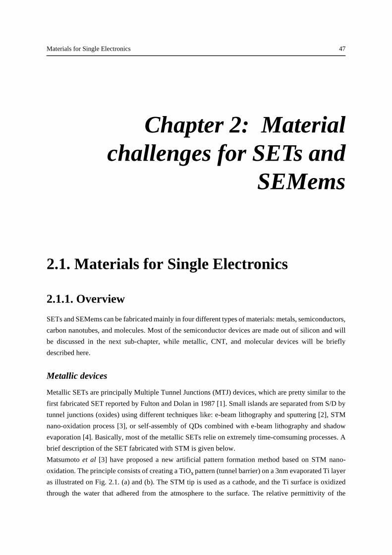
Materials for Single Electronics 47
Chapter 2: Materialchallenges for SETs and
SEMems
2.1. Materials for Single Electronics
2.1.1. Overview
SETs and SEMems can be fabricated mainly in four different types of materials: metals, semiconductors,
carbon nanotubes, and molecules. Most of the semiconductor devices are made out of silicon and will
be discussed in the next sub-chapter, while metallic, CNT, and molecular devices will be briefly
described here.
Metallic devices
Metallic SETs are principally Multiple Tunnel Junctions (MTJ) devices, which are pretty similar to the
first fabricated SET reported by Fulton and Dolan in 1987 [1]. Small islands are separated from S/D by
tunnel junctions (oxides) using different techniques like: e-beam lithography and sputtering [2], STM
nano-oxidation process [3], or self-assembly of QDs combined with e-beam lithography and shadow
evaporation [4]. Basically, most of the metallic SETs relie on extremely time-comsuming processes. A
brief description of the SET fabricated with STM is given below.
Matsumoto et al [3] have proposed a new artificial pattern formation method based on STM nano-
oxidation. The principle consists of creating a TiOx pattern (tunnel barrier) on a 3nm evaporated Ti layer
as illustrated on Fig. 2.1. (a) and (b). The STM tip is used as a cathode, and the Ti surface is oxidized
through the water that adhered from the atmosphere to the surface. The relative permittivity of the
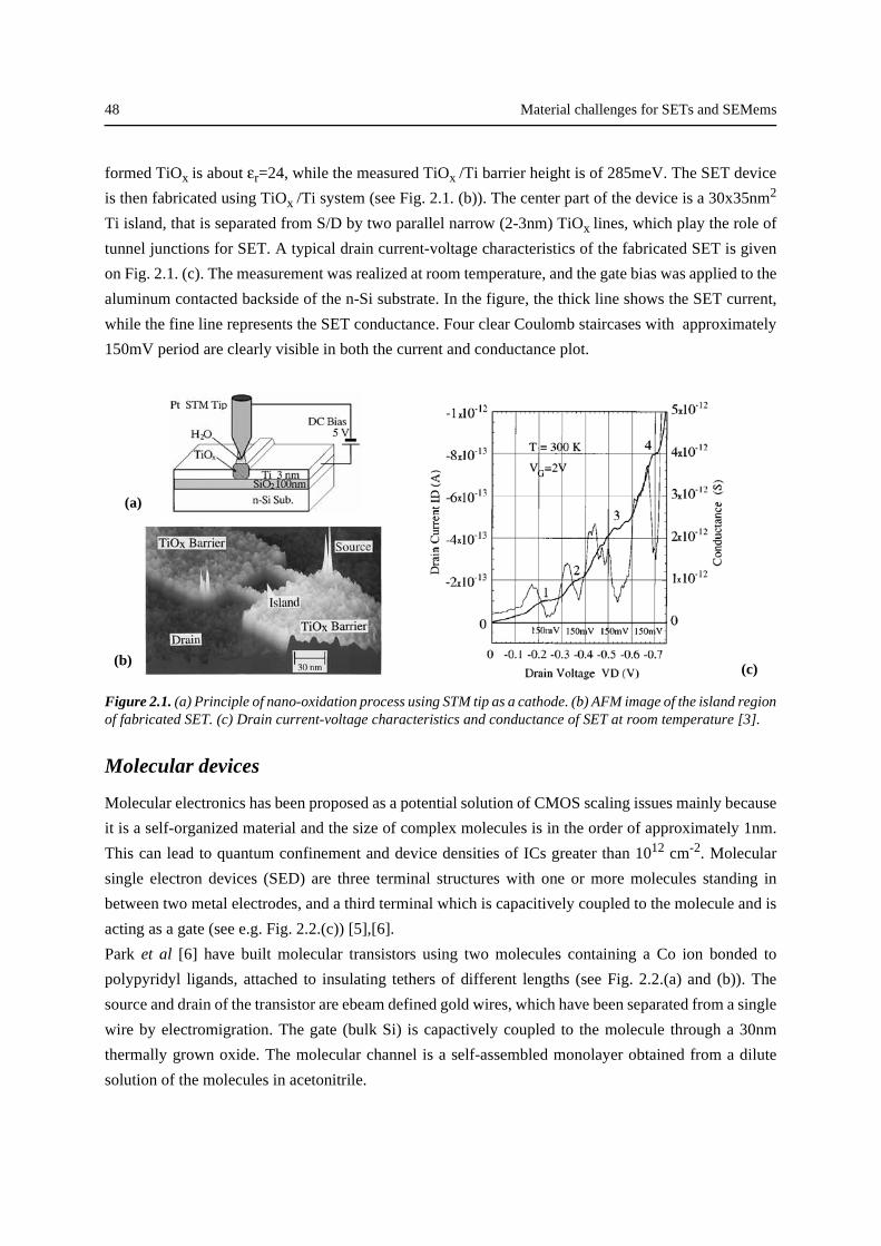
48 Material challenges for SETs and SEMems
formed TiOx is about εr=24, while the measured TiOx /Ti barrier height is of 285meV. The SET device
is then fabricated using TiOx /Ti system (see Fig. 2.1. (b)). The center part of the device is a 30x35nm2
Ti island, that is separated from S/D by two parallel narrow (2-3nm) TiOx lines, which play the role of
tunnel junctions for SET. A typical drain current-voltage characteristics of the fabricated SET is given
on Fig. 2.1. (c). The measurement was realized at room temperature, and the gate bias was applied to the
aluminum contacted backside of the n-Si substrate. In the figure, the thick line shows the SET current,
while the fine line represents the SET conductance. Four clear Coulomb staircases with approximately
150mV period are clearly visible in both the current and conductance plot.
Figure 2.1. (a) Principle of nano-oxidation process using STM tip as a cathode. (b) AFM image of the island regionof fabricated SET. (c) Drain current-voltage characteristics and conductance of SET at room temperature [3].
Molecular devices
Molecular electronics has been proposed as a potential solution of CMOS scaling issues mainly because
it is a self-organized material and the size of complex molecules is in the order of approximately 1nm.
This can lead to quantum confinement and device densities of ICs greater than 1012 cm-2. Molecular
single electron devices (SED) are three terminal structures with one or more molecules standing in
between two metal electrodes, and a third terminal which is capacitively coupled to the molecule and is
acting as a gate (see e.g. Fig. 2.2.(c)) [5],[6].
Park et al [6] have built molecular transistors using two molecules containing a Co ion bonded to
polypyridyl ligands, attached to insulating tethers of different lengths (see Fig. 2.2.(a) and (b)). The
source and drain of the transistor are ebeam defined gold wires, which have been separated from a single
wire by electromigration. The gate (bulk Si) is capactively coupled to the molecule through a 30nm
thermally grown oxide. The molecular channel is a self-assembled monolayer obtained from a dilute
solution of the molecules in acetonitrile.
(a)
(b)(c)
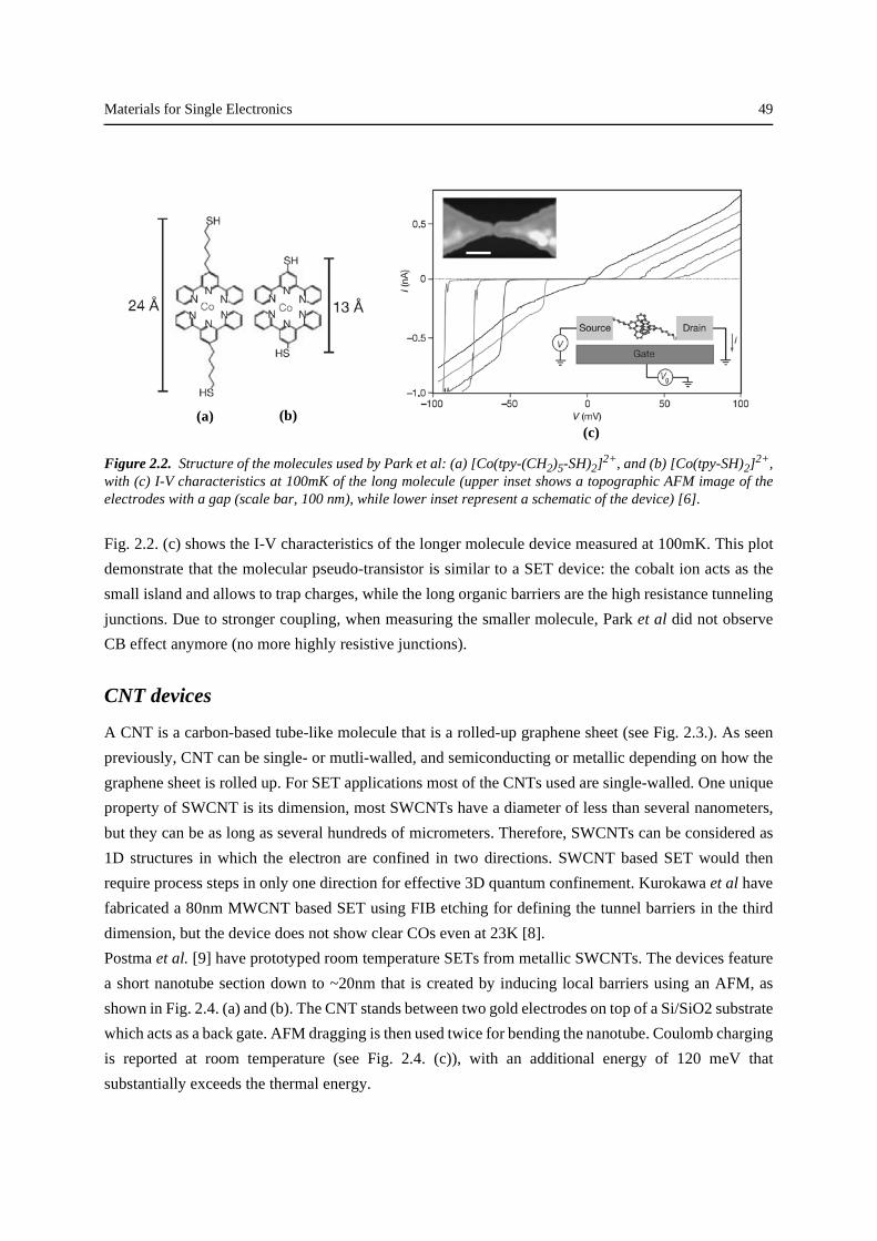
Materials for Single Electronics 49
Figure 2.2. Structure of the molecules used by Park et al: (a) [Co(tpy-(CH2)5-SH)2]2+, and (b) [Co(tpy-SH)2]2+,with (c) I-V characteristics at 100mK of the long molecule (upper inset shows a topographic AFM image of theelectrodes with a gap (scale bar, 100 nm), while lower inset represent a schematic of the device) [6].
Fig. 2.2. (c) shows the I-V characteristics of the longer molecule device measured at 100mK. This plot
demonstrate that the molecular pseudo-transistor is similar to a SET device: the cobalt ion acts as the
small island and allows to trap charges, while the long organic barriers are the high resistance tunneling
junctions. Due to stronger coupling, when measuring the smaller molecule, Park et al did not observe
CB effect anymore (no more highly resistive junctions).
CNT devices
A CNT is a carbon-based tube-like molecule that is a rolled-up graphene sheet (see Fig. 2.3.). As seen
previously, CNT can be single- or mutli-walled, and semiconducting or metallic depending on how the
graphene sheet is rolled up. For SET applications most of the CNTs used are single-walled. One unique
property of SWCNT is its dimension, most SWCNTs have a diameter of less than several nanometers,
but they can be as long as several hundreds of micrometers. Therefore, SWCNTs can be considered as
1D structures in which the electron are confined in two directions. SWCNT based SET would then
require process steps in only one direction for effective 3D quantum confinement. Kurokawa et al have
fabricated a 80nm MWCNT based SET using FIB etching for defining the tunnel barriers in the third
dimension, but the device does not show clear COs even at 23K [8].
Postma et al. [9] have prototyped room temperature SETs from metallic SWCNTs. The devices feature
a short nanotube section down to ~20nm that is created by inducing local barriers using an AFM, as
shown in Fig. 2.4. (a) and (b). The CNT stands between two gold electrodes on top of a Si/SiO2 substrate
which acts as a back gate. AFM dragging is then used twice for bending the nanotube. Coulomb charging
is reported at room temperature (see Fig. 2.4. (c)), with an additional energy of 120 meV that
substantially exceeds the thermal energy.
(a)(c)
(b)
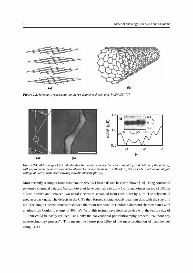
50 Material challenges for SETs and SEMems
Figure 2.3. Schematic representation of: (a) graphene sheets, and (b) SWCNT [7].
Figure 2.4. AFM image of (a) a double-buckle nanotube device (Au electrode at top and bottom of the picture),with (b) zoom on the active part of double-buckle device (scale bar is 20nm); (c) device COs as a function of gatevoltage at 260 K, with inset showing a dI/dV intensity plot [9].
More recently, a simpler room temperature SWCNT based device has been shown [10]. Using controlled
patterned chemical catalyst Matsumoto et al have been able to grow 1-2nm nanotubes on top of 100nm
silicon dioxide and between two metal electrodes separated from each other by 4µm. The substrate is
used as a back gate. The defects in the CNT then formed spontaneously quantum dots with the size of 1
nm. The single electron transistor showed the room-temperature Coulomb diamond characteristics with
an ultra-high Coulomb energy of 400meV. With this technology, electron device with the feature size of
1–2 nm could be easily realized using only the conventional photolithography process, ‘‘without any
nano-technology process’’. This means the future possibility of the mass-production of nanodevices
using CNTs.
(a) (b)
(a) (b)(c)
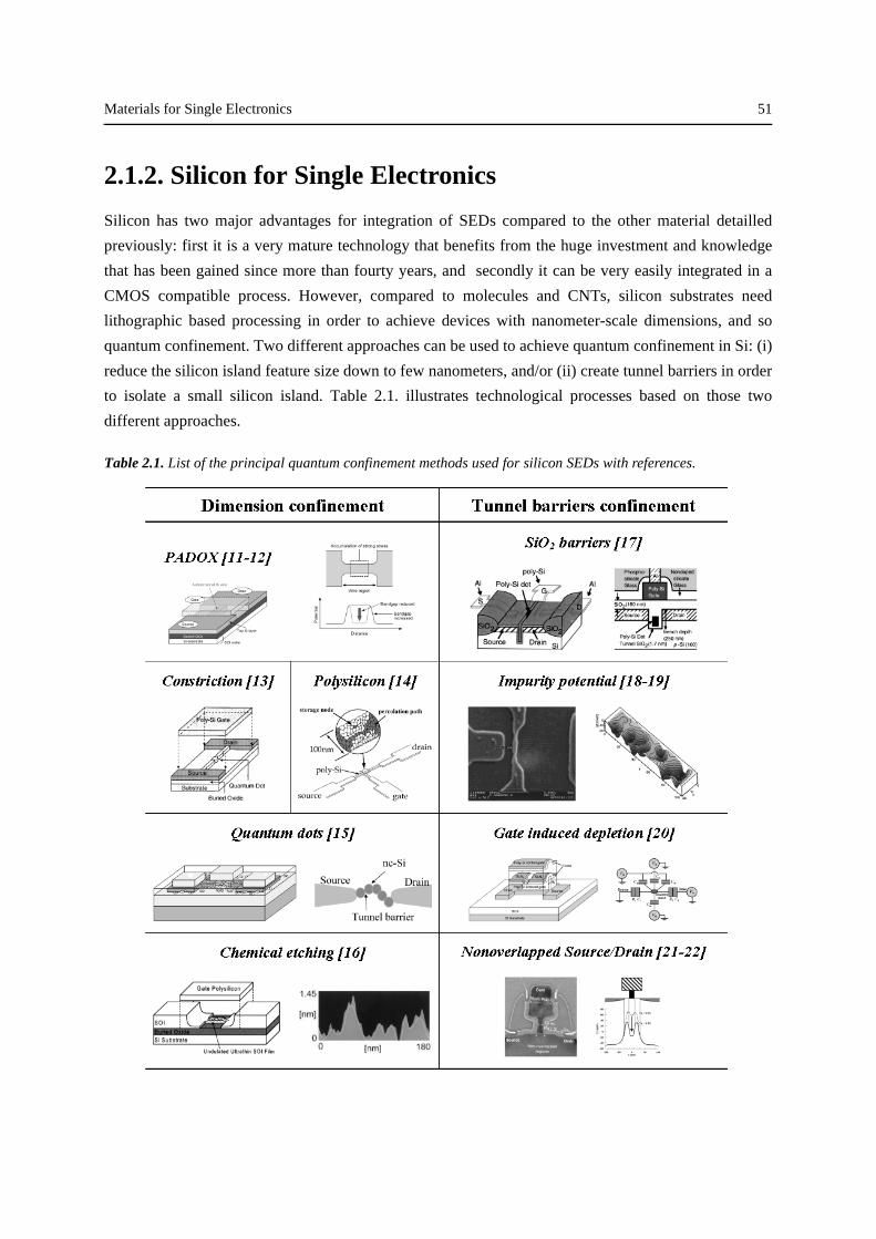
Materials for Single Electronics 51
2.1.2. Silicon for Single Electronics
Silicon has two major advantages for integration of SEDs compared to the other material detailled
previously: first it is a very mature technology that benefits from the huge investment and knowledge
that has been gained since more than fourty years, and secondly it can be very easily integrated in a
CMOS compatible process. However, compared to molecules and CNTs, silicon substrates need
lithographic based processing in order to achieve devices with nanometer-scale dimensions, and so
quantum confinement. Two different approaches can be used to achieve quantum confinement in Si: (i)
reduce the silicon island feature size down to few nanometers, and/or (ii) create tunnel barriers in order
to isolate a small silicon island. Table 2.1. illustrates technological processes based on those two
different approaches.
Table 2.1. List of the principal quantum confinement methods used for silicon SEDs with references.
52 Material challenges for SETs and SEMems
Quantum confinement through island dimension reduction is mainly achieved using extremely well
controlled thermal oxidation of monocrystalline silicon, high resolution lithographic tools like ebeam,
or a combination of both methods [11], [13]. Another technique that has been succesfully demonstrated
by Uchida et al [16] is a combination of silicon oxidation for the reduction of the silicon thickness (SOI
substrate), combined with wet chemical etching using an alkaline-based solution (choline) for undulated
silicon channel. The nanoscale undulation in the ultrathin film results in the formation of nanoscale
potential fluctuations and CB effects. Finally, Si nanoscale dimensions can be obtained naturally through
adapted deposition methods like for Si quantum dots [15] and ultra-thin polySi [14].
Tunnel barrier confinement can be achieved either through fabricated tunnel barriers like SiO2 [17], or
through electrostatically defined tunnel barries due to: impurity fluctuations in a very narrow device
(potential wells along the channel) [18], controlled gate induced depletion at both ends of the channel
[20], or nonoverlapped S/D contacts giving high potential barriers at the S/D-channel interfaces [21].
2.1.3. Nanograin polysilicon
Polycrystalline silicon is a widely used material in the semiconductor industry, as poly-gate for CMOS
devices, NVM, and DRAM, as the active layer of thin-film transistors (TFT), as passive resistors, local
interconnects, or microelectromechanical systems (MEMS). This success is a combination between a
low cost material and a large range of deposition temperatures, together with a tunability of the structural
and physical properties of polySi. Indeed, polySi properties can be tuned during deposition, but also after
with annealing sequences and/or doping. Finally, polySi is a very mature material as it has been used in
semiconductors for more than three decades.
PolySi can be considered as a natural multi-islands material (see 1.4.5.“Multi-island SETs”) composed
of monocrystalline silicon grain islands separated by grain boundaries. PolySi grain size can be
adequatly controlled thermally and reduced to few nanometers. Consequently, each island or at least the
majority of the islands can be considered as QDs. These QDs may behave as excellent traps for one or
few electrons as it has already been demonstrated in SET [23], and SEMem applications (see
1.4.6.“Multi-island Single Electron Memory”) [14], [24]. Hence, optimized grain size polySi is an
excellent candidate for future nanoelectronics, and this is why we choose it for our research.
Technology developments for ultra-thin sub-10nm polysilicon film 53
2.2. Technology developments for ultra-thin sub-10nm polysilicon film
The target of this technological part is to achieve the realization of a 10nm or less thin polySi film with
equivalent grain sizes. For this purpose, two radically different approaches have been evaluated: the first
one consists in a deposition of this layer by standard low pressure chemical vapour deposition (LPCVD),
whereas the second approach consists in a thinning of deposited amorphous silicon (aSi), or polySi film
(e.g. 100nm). The restrictions on this technological part are twofold: achievement of nanograin ultra-thin
10nm polySi film with fully CMOS compatible process, and realization of the devices with equipments
that are mainly available at the Centre of Micro/Nanotechnology (CMI) of EPFL.
Three different deposition process have been evaluated for the realization of LPCVD deposited polySi
film: (i) a direct LPCVD polySi deposition; (ii) a two-steps Hemispherical Silicon Grain (HSG)
deposition; and finally (iii) a two-steps aSi deposition followed by crystallization annealing. For the
thinning process, four different solutions have been tested: (i) sacrificial oxidation; (ii) dry Reactive Ion
Etching (RIE); wet chemical etching using (iv) SECCO, or (v) poly-etch based solutions.
The implantation of the ultra-thin polysilicon film was also pretty challenging. Grain size specifiactions
(~10nm) has prevented the use of a standard implantation process followed by high temperature anneal.
Indeed, high temperature activation anneal would induce an unacceptable polySi grain growth. Hence,
a novel method of implantation has been developed together with Ion Beam Services (IBS) [25]: a "hot"
implantation at 500°C providing a combinated implantation and activation.
2.2.1. LPCVD technology
Introduction
PolySi LPCVD involves the thermal decomposition of silane (SiH4) to form elementary silicon and
molecular hydrogen:
(2.1)
In a standard LPCVD reactor, gases are continuously introduced into the reactor and unused gases and
reaction products are also continuously removed. The deposition process is influenced by both the
kinetic factors and the thermodynamics of the decomposition. Hence, the main parameters that governs
the deposition rate, but also the physical properties of the deposited Si layers are: (i) the deposition
temperature, (ii) the pressure in the reactor chamber, and (iii) the flux of silane through the reactor. Fig.
SiH4 g( ) Si s( ) 2H+ 2 g( )→
54 Material challenges for SETs and SEMems
2.5. gives the crystalline structure of the deposited silicon as a function of the deposition temperature and
the LPCVD chamber pressure (all the results are extracted from litterature). The straight black lines A
and B represent the limits between aSi, polySi and an in-between transition region of rugged surface
polySi as-defined by [26]. The black squarred markers stand for amorphous deposited Si films [27]-[31],
whereas the gray triangular markers correspond to polySi layers [32]-[36].
Figure 2.5. Crystalline structure of deposited Si films as a fuction of temperature and silane pressure. Blacksquarred markers correspond to aSi, while gray triangular makers stand for polySi.
One can see that a combination of high temperature and low silane pressure leads to the formation of
completely polycrystalline Si, while lower temperature combined with higher pressure gives a fully
amorphous Si layer. Between those two regimes, the deposited films are either partially crystallized or
totally crystallized with well separated grains and a rugged surface. This transition region is between
560°C and 590°C for a chamber pressure of 150mT [37]. Under those conditions, an increase of the
silane pressure increases the amorphization level of the layer [38]. It has already been shown that aSi can
be deposited at 580°C and 200mT, and when the deposition temperature is decreased, the layer
uniformity but also the surface roughness is improved [39].
Experimental specifications
The substrates used for the deposition tests were 100mm ‹100› oriented, boron-doped p-type silicon
wafers. A silicon oxide layer has been grown by thermal oxidation prior to any Si deposition. All the
silicon layers have been carried out by thermal decomposition of pure silane (SiH4) in a
CENTROTHERM conventional horizontal hot-wall type LPCVD reactor [40]. The experimental
conditions tested for either amorphous or polycrystalline silicon are represented on Fig. 2.6. Amorphous
silicon has been deposited at temperatures between 475°C and 525°C, for silane pressure ranging from
100mT up to 400mT, while polySi has been deposited between 580°C and 640°C, for silane pressure
ranging from 60mT up to 200mT.
0.01
0.1
1
10
500 525 550 575 600 625 650
Temperature (°C)
Pre
ssur
e (T
orr)
amorphous
polycrystalline
A
Btransition
region
Technology developments for ultra-thin sub-10nm polysilicon film 55
Figure 2.6. Experimental conditions used for the deposition of aSi (black squares) and polySi (grey triangles). Theblack A’ and B’ lines show extrapolated limits between amorphous and polycrystalline Si structure [26].
For each experiments the silane flux has been maintained at 30sccm in the back of the reactor, but
different depostion time have been used in order to determine the adequate deposition rate and so to
achieve the minimum thickness goal of less than 10nm layers. The film thicknesses have been measured
by spectro-reflectometry. The surface morphology was observed by SEM and AFM. The microstructure
of the films was investigated by transmission electron microscopy (TEM).
Direct polySi LPCVD
Table 2.1. summarizes some of the results obtained for the direct polySi deposition. Three different
processes at constant pressure but different temperatures are presented. The deposition rates were
calculated from the slope of the calibration curves based on multiple deposition times under similar
temperature and pressure conditions. The continuous surface at (-) represents the minimum film
thickness needed to get a continuous polySi layer fully recovering the wafer (without porosity).
Table 2.1. Characteristics summary of three polySi processes.
We can see that the deposition rate tends to be important for less than 100Å films. Even with a
temperature as low as 600°C, the deposition rate is about 36Å/min. In this case, our application would
require a less than three minutes process, which is not controllable in a conventional reactor. It also
appears that the temperature affects the surface recovery: the higher the temperature, the thicker the
0.01
0.1
1
450 475 500 525 550 575 600 625 650
Temperature (°C)
Pre
ssur
e (T
orr)
amorphous
polycrystalline
A'B'
Dep. temp. (°C)
Pressure (mT)
Dep. rate (Å/min)
Cont. surface at – (Å)
640 100 68 330 620 100 60 280 600 100 36 200
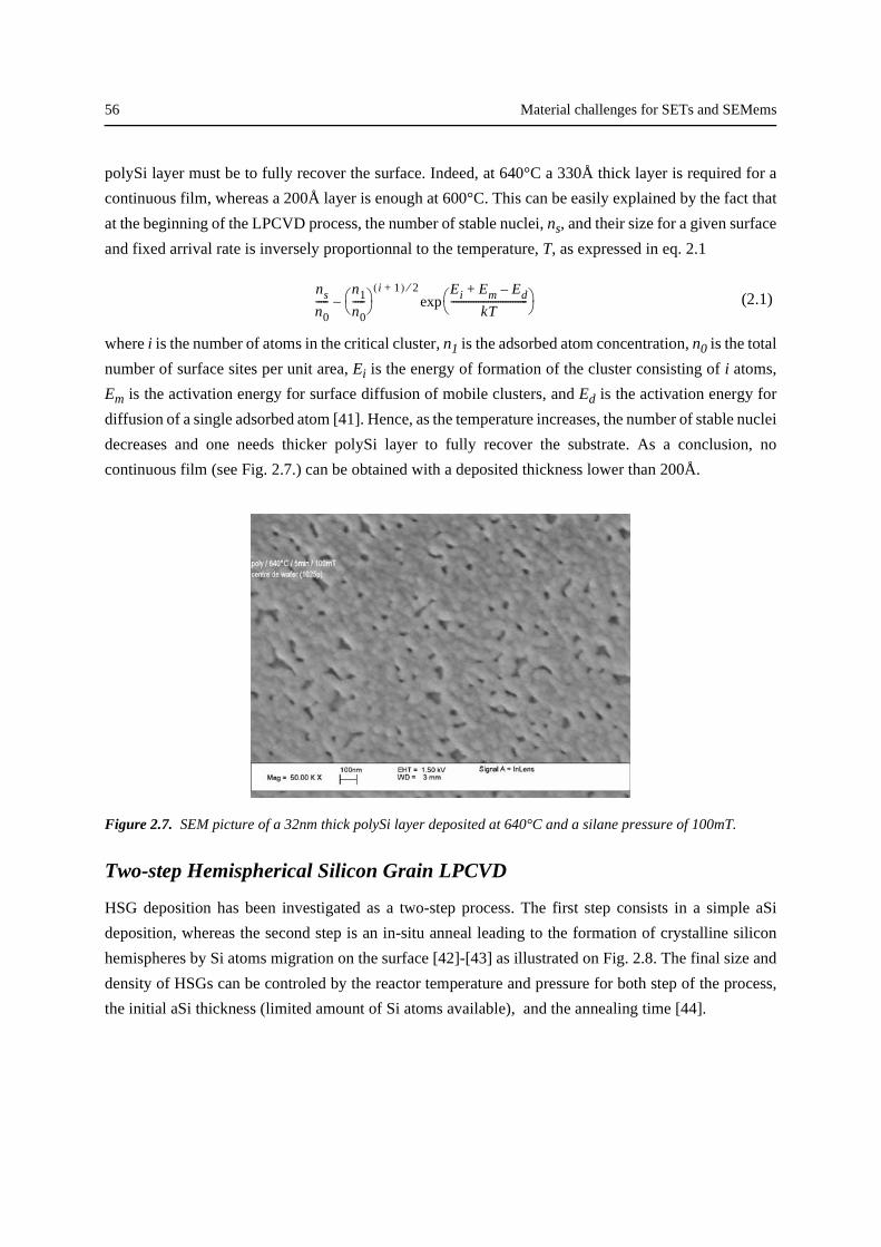
56 Material challenges for SETs and SEMems
polySi layer must be to fully recover the surface. Indeed, at 640°C a 330Å thick layer is required for a
continuous film, whereas a 200Å layer is enough at 600°C. This can be easily explained by the fact that
at the beginning of the LPCVD process, the number of stable nuclei, ns, and their size for a given surface
and fixed arrival rate is inversely proportionnal to the temperature, T, as expressed in eq. 2.1
(2.1)
where i is the number of atoms in the critical cluster, n1 is the adsorbed atom concentration, n0 is the total
number of surface sites per unit area, Ei is the energy of formation of the cluster consisting of i atoms,
Em is the activation energy for surface diffusion of mobile clusters, and Ed is the activation energy for
diffusion of a single adsorbed atom [41]. Hence, as the temperature increases, the number of stable nuclei
decreases and one needs thicker polySi layer to fully recover the substrate. As a conclusion, no
continuous film (see Fig. 2.7.) can be obtained with a deposited thickness lower than 200Å.
Figure 2.7. SEM picture of a 32nm thick polySi layer deposited at 640°C and a silane pressure of 100mT.
Two-step Hemispherical Silicon Grain LPCVD
HSG deposition has been investigated as a two-step process. The first step consists in a simple aSi
deposition, whereas the second step is an in-situ anneal leading to the formation of crystalline silicon
hemispheres by Si atoms migration on the surface [42]-[43] as illustrated on Fig. 2.8. The final size and
density of HSGs can be controled by the reactor temperature and pressure for both step of the process,
the initial aSi thickness (limited amount of Si atoms available), and the annealing time [44].
ns
n0-----
n1
n0-----⎝ ⎠⎛ ⎞
i 1+( ) 2⁄ Ei Em Ed–+
kT-------------------------------⎝ ⎠⎛ ⎞exp∼
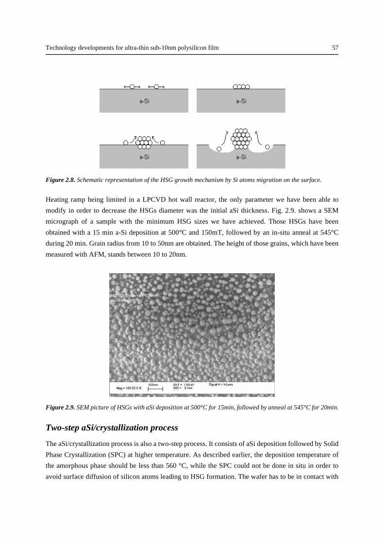
Technology developments for ultra-thin sub-10nm polysilicon film 57
Figure 2.8. Schematic representation of the HSG growth mechanism by Si atoms migration on the surface.
Heating ramp being limited in a LPCVD hot wall reactor, the only parameter we have been able to
modify in order to decrease the HSGs diameter was the initial aSi thickness. Fig. 2.9. shows a SEM
micrograph of a sample with the minimum HSG sizes we have achieved. Those HSGs have been
obtained with a 15 min a-Si deposition at 500°C and 150mT, followed by an in-situ anneal at 545°C
during 20 min. Grain radius from 10 to 50nm are obtained. The height of those grains, which have been
measured with AFM, stands between 10 to 20nm.
Figure 2.9. SEM picture of HSGs with aSi deposition at 500°C for 15min, followed by anneal at 545°C for 20min.
Two-step aSi/crystallization process
The aSi/crystallization process is also a two-step process. It consists of aSi deposition followed by Solid
Phase Crystallization (SPC) at higher temperature. As described earlier, the deposition temperature of
the amorphous phase should be less than 560 °C, while the SPC could not be done in situ in order to
avoid surface diffusion of silicon atoms leading to HSG formation. The wafer has to be in contact with
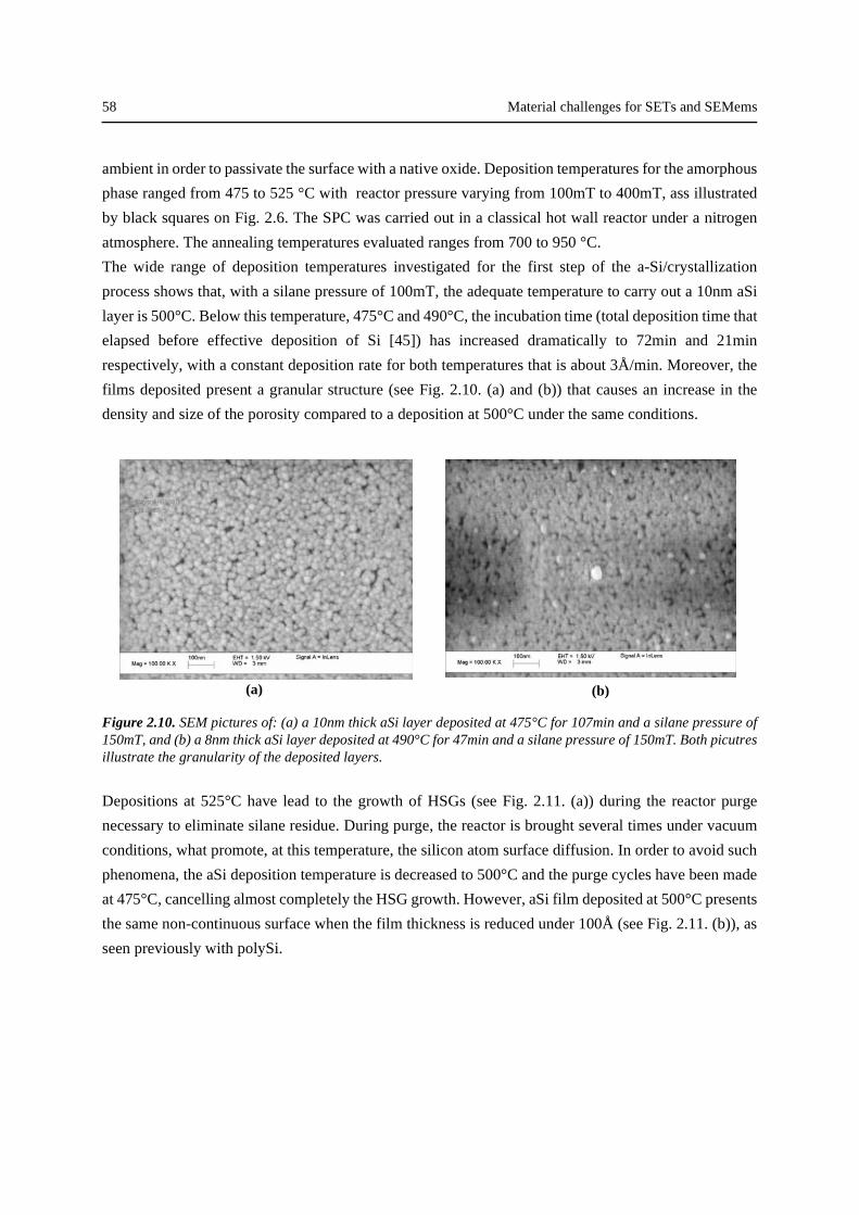
58 Material challenges for SETs and SEMems
ambient in order to passivate the surface with a native oxide. Deposition temperatures for the amorphous
phase ranged from 475 to 525 °C with reactor pressure varying from 100mT to 400mT, ass illustrated
by black squares on Fig. 2.6. The SPC was carried out in a classical hot wall reactor under a nitrogen
atmosphere. The annealing temperatures evaluated ranges from 700 to 950 °C.
The wide range of deposition temperatures investigated for the first step of the a-Si/crystallization
process shows that, with a silane pressure of 100mT, the adequate temperature to carry out a 10nm aSi
layer is 500°C. Below this temperature, 475°C and 490°C, the incubation time (total deposition time that
elapsed before effective deposition of Si [45]) has increased dramatically to 72min and 21min
respectively, with a constant deposition rate for both temperatures that is about 3Å/min. Moreover, the
films deposited present a granular structure (see Fig. 2.10. (a) and (b)) that causes an increase in the
density and size of the porosity compared to a deposition at 500°C under the same conditions.
Figure 2.10. SEM pictures of: (a) a 10nm thick aSi layer deposited at 475°C for 107min and a silane pressure of150mT, and (b) a 8nm thick aSi layer deposited at 490°C for 47min and a silane pressure of 150mT. Both picutresillustrate the granularity of the deposited layers.
Depositions at 525°C have lead to the growth of HSGs (see Fig. 2.11. (a)) during the reactor purge
necessary to eliminate silane residue. During purge, the reactor is brought several times under vacuum
conditions, what promote, at this temperature, the silicon atom surface diffusion. In order to avoid such
phenomena, the aSi deposition temperature is decreased to 500°C and the purge cycles have been made
at 475°C, cancelling almost completely the HSG growth. However, aSi film deposited at 500°C presents
the same non-continuous surface when the film thickness is reduced under 100Å (see Fig. 2.11. (b)), as
seen previously with polySi.
(a) (b)
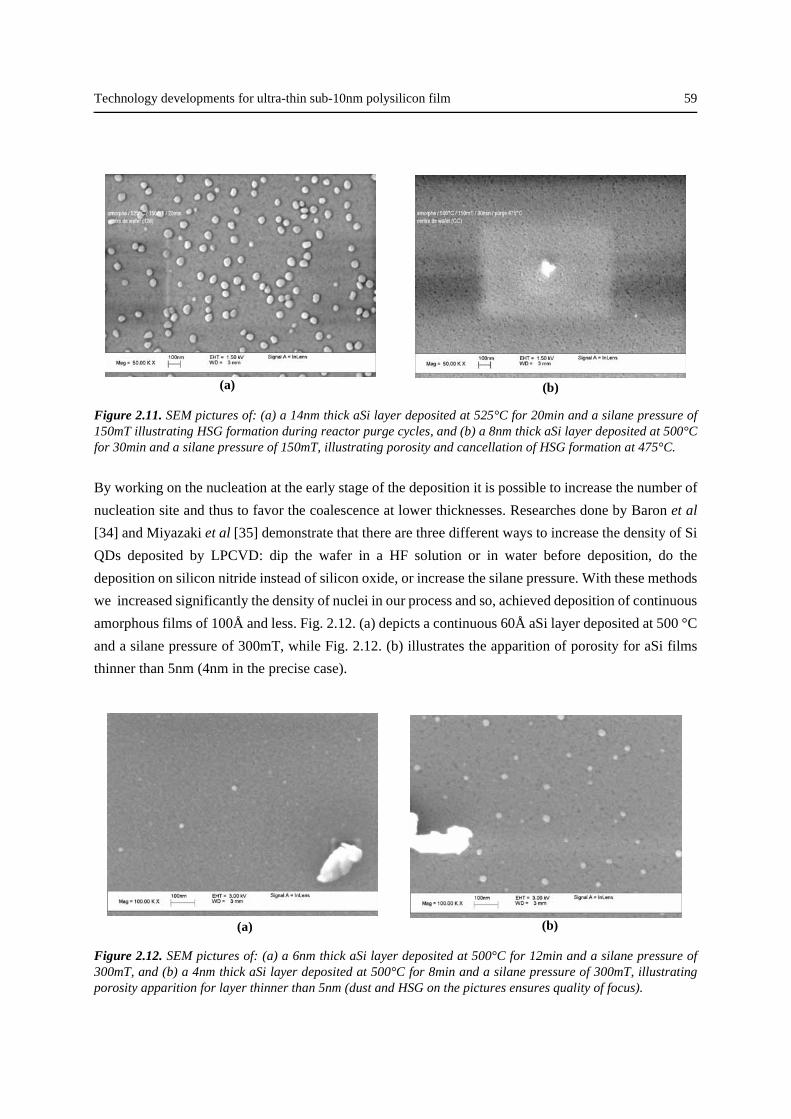
Technology developments for ultra-thin sub-10nm polysilicon film 59
Figure 2.11. SEM pictures of: (a) a 14nm thick aSi layer deposited at 525°C for 20min and a silane pressure of150mT illustrating HSG formation during reactor purge cycles, and (b) a 8nm thick aSi layer deposited at 500°Cfor 30min and a silane pressure of 150mT, illustrating porosity and cancellation of HSG formation at 475°C.
By working on the nucleation at the early stage of the deposition it is possible to increase the number of
nucleation site and thus to favor the coalescence at lower thicknesses. Researches done by Baron et al
[34] and Miyazaki et al [35] demonstrate that there are three different ways to increase the density of Si
QDs deposited by LPCVD: dip the wafer in a HF solution or in water before deposition, do the
deposition on silicon nitride instead of silicon oxide, or increase the silane pressure. With these methods
we increased significantly the density of nuclei in our process and so, achieved deposition of continuous
amorphous films of 100Å and less. Fig. 2.12. (a) depicts a continuous 60Å aSi layer deposited at 500 °C
and a silane pressure of 300mT, while Fig. 2.12. (b) illustrates the apparition of porosity for aSi films
thinner than 5nm (4nm in the precise case).
Figure 2.12. SEM pictures of: (a) a 6nm thick aSi layer deposited at 500°C for 12min and a silane pressure of300mT, and (b) a 4nm thick aSi layer deposited at 500°C for 8min and a silane pressure of 300mT, illustratingporosity apparition for layer thinner than 5nm (dust and HSG on the pictures ensures quality of focus).
(a) (b)
(a) (b)
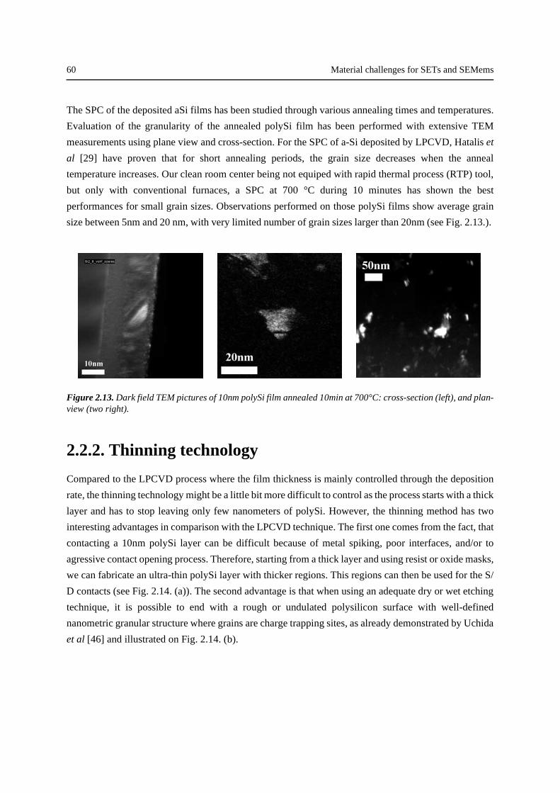
60 Material challenges for SETs and SEMems
The SPC of the deposited aSi films has been studied through various annealing times and temperatures.
Evaluation of the granularity of the annealed polySi film has been performed with extensive TEM
measurements using plane view and cross-section. For the SPC of a-Si deposited by LPCVD, Hatalis et
al [29] have proven that for short annealing periods, the grain size decreases when the anneal
temperature increases. Our clean room center being not equiped with rapid thermal process (RTP) tool,
but only with conventional furnaces, a SPC at 700 °C during 10 minutes has shown the best
performances for small grain sizes. Observations performed on those polySi films show average grain
size between 5nm and 20 nm, with very limited number of grain sizes larger than 20nm (see Fig. 2.13.).
Figure 2.13. Dark field TEM pictures of 10nm polySi film annealed 10min at 700°C: cross-section (left), and plan-view (two right).
2.2.2. Thinning technology
Compared to the LPCVD process where the film thickness is mainly controlled through the deposition
rate, the thinning technology might be a little bit more difficult to control as the process starts with a thick
layer and has to stop leaving only few nanometers of polySi. However, the thinning method has two
interesting advantages in comparison with the LPCVD technique. The first one comes from the fact, that
contacting a 10nm polySi layer can be difficult because of metal spiking, poor interfaces, and/or to
agressive contact opening process. Therefore, starting from a thick layer and using resist or oxide masks,
we can fabricate an ultra-thin polySi layer with thicker regions. This regions can then be used for the S/
D contacts (see Fig. 2.14. (a)). The second advantage is that when using an adequate dry or wet etching
technique, it is possible to end with a rough or undulated polysilicon surface with well-defined
nanometric granular structure where grains are charge trapping sites, as already demonstrated by Uchida
et al [46] and illustrated on Fig. 2.14. (b).
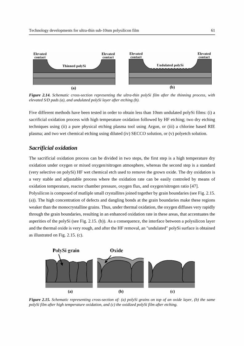
Technology developments for ultra-thin sub-10nm polysilicon film 61
Figure 2.14. Schematic cross-section representing the ultra-thin polySi film after the thinning process, withelevated S/D pads (a), and undulated polySi layer after etching (b).
Five different methods have been tested in order to obtain less than 10nm undulated polySi films: (i) a
sacrificial oxidation process with high temperature oxidation followed by HF etching; two dry etching
techniques using (ii) a pure physical etching plasma tool using Argon, or (iii) a chlorine based RIE
plasma; and two wet chemical etching using diluted (iv) SECCO solution, or (v) polyetch solution.
Sacrificial oxidation
The sacrificial oxidation process can be divided in two steps, the first step is a high temperature dry
oxidation under oxygen or mixed oxygen/nitrogen atmosphere, whereas the second step is a standard
(very selective on polySi) HF wet chemical etch used to remove the grown oxide. The dry oxidation is
a very stable and adjustable process where the oxidation rate can be easily controled by means of
oxidation temperature, reactor chamber pressure, oxygen flux, and oxygen/nitrogen ratio [47].
Polysilicon is composed of mutliple small crystallites joined together by grain boundaries (see Fig. 2.15.
(a)). The high concentration of defects and dangling bonds at the grain boundaries make these regions
weaker than the monocrystalline grains. Thus, under thermal oxidation, the oxygen diffuses very rapidly
through the grain boundaries, resulting in an enhanced oxidation rate in these areas, that accentuates the
asperities of the polySi (see Fig. 2.15. (b)). As a consequence, the interface between a polysilicon layer
and the thermal oxide is very rough, and after the HF removal, an "undulated" polySi surface is obtained
as illustrated on Fig. 2.15. (c).
Figure 2.15. Schematic representing cross-section of: (a) polySi grains on top of an oxide layer, (b) the samepolySi film after high temperature oxidation, and (c) the oxidized polySi film after etching.
(a) (b)
(a) (b) (c)
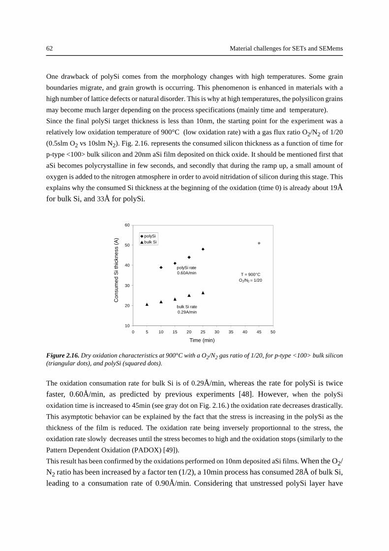
62 Material challenges for SETs and SEMems
One drawback of polySi comes from the morphology changes with high temperatures. Some grain
boundaries migrate, and grain growth is occurring. This phenomenon is enhanced in materials with a
high number of lattice defects or natural disorder. This is why at high temperatures, the polysilicon grains
may become much larger depending on the process specifications (mainly time and temperature).
Since the final polySi target thickness is less than 10nm, the starting point for the experiment was a
relatively low oxidation temperature of 900°C (low oxidation rate) with a gas flux ratio O2/N2 of 1/20
(0.5slm O2 vs 10slm N2). Fig. 2.16. represents the consumed silicon thickness as a function of time for
p-type <100> bulk silicon and 20nm aSi film deposited on thick oxide. It should be mentioned first that
aSi becomes polycrystalline in few seconds, and secondly that during the ramp up, a small amount of
oxygen is added to the nitrogen atmosphere in order to avoid nitridation of silicon during this stage. This
explains why the consumed Si thickness at the beginning of the oxidation (time 0) is already about 19Å
for bulk Si, and 33Å for polySi.
Figure 2.16. Dry oxidation characteristics at 900°C with a O2/N2 gas ratio of 1/20, for p-type <100> bulk silicon(triangular dots), and polySi (squared dots).
The oxidation consumation rate for bulk Si is of 0.29Å/min, whereas the rate for polySi is twice
faster, 0.60Å/min, as predicted by previous experiments [48]. However, when the polySi
oxidation time is increased to 45min (see gray dot on Fig. 2.16.) the oxidation rate decreases drastically.
This asymptotic behavior can be explained by the fact that the stress is increasing in the polySi as the
thickness of the film is reduced. The oxidation rate being inversely proportionnal to the stress, the
oxidation rate slowly decreases until the stress becomes to high and the oxidation stops (similarly to the
Pattern Dependent Oxidation (PADOX) [49]).
This result has been confirmed by the oxidations performed on 10nm deposited aSi films. When the O2/
N2 ratio has been increased by a factor ten (1/2), a 10min process has consumed 28Å of bulk Si,
leading to a consumation rate of 0.90Å/min. Considering that unstressed polySi layer have
10
20
30
40
50
60
0 5 10 15 20 25 30 35 40 45 50
Time (min)
Con
sum
ed S
i thi
ckne
ss (
A) polySi
bulk Si
T = 900°CO2/N2 = 1/20
polySi rate0.60A/min
bulk Si rate0.29A/min
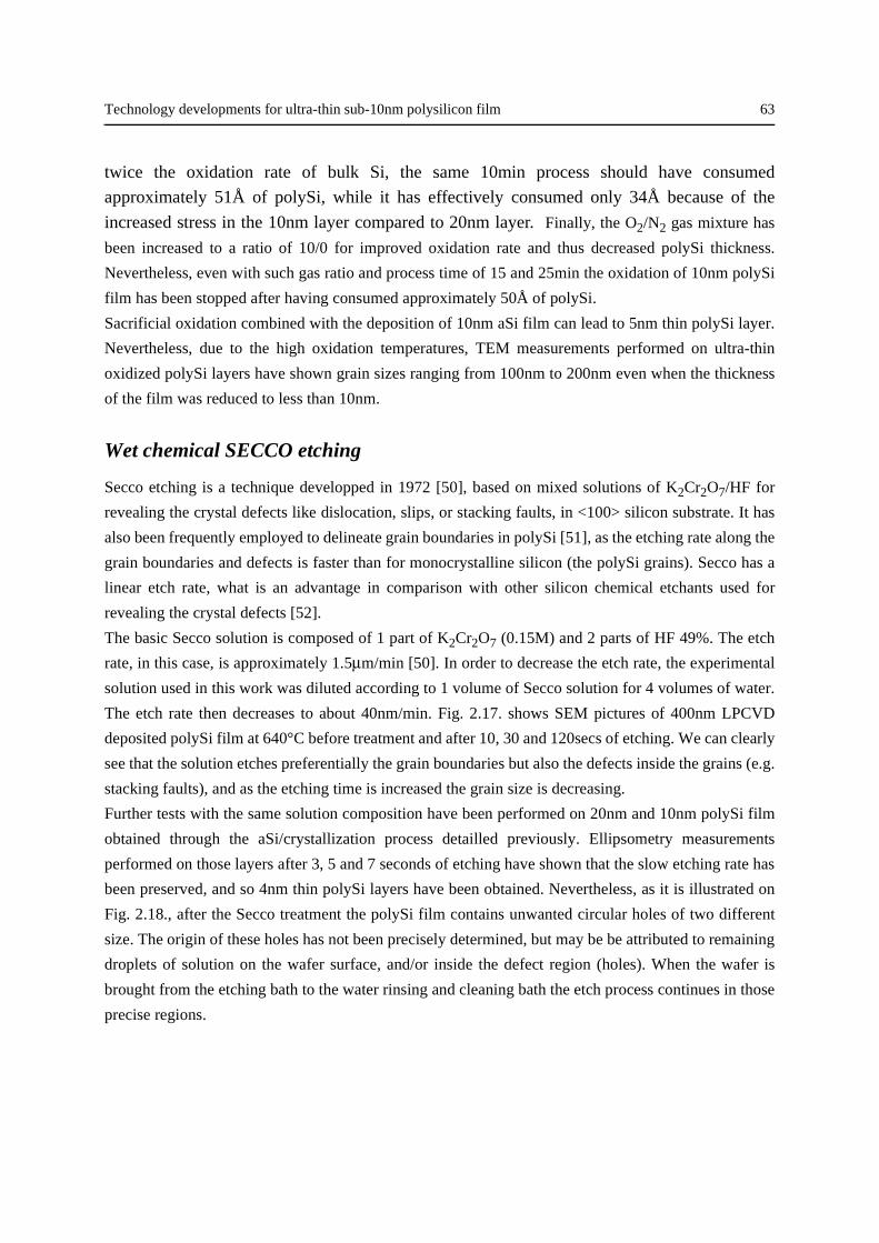
Technology developments for ultra-thin sub-10nm polysilicon film 63
twice the oxidation rate of bulk Si, the same 10min process should have consumed
approximately 51Å of polySi, while it has effectively consumed only 34Å because of the
increased stress in the 10nm layer compared to 20nm layer. Finally, the O2/N2 gas mixture has
been increased to a ratio of 10/0 for improved oxidation rate and thus decreased polySi thickness.
Nevertheless, even with such gas ratio and process time of 15 and 25min the oxidation of 10nm polySi
film has been stopped after having consumed approximately 50Å of polySi.
Sacrificial oxidation combined with the deposition of 10nm aSi film can lead to 5nm thin polySi layer.
Nevertheless, due to the high oxidation temperatures, TEM measurements performed on ultra-thin
oxidized polySi layers have shown grain sizes ranging from 100nm to 200nm even when the thickness
of the film was reduced to less than 10nm.
Wet chemical SECCO etching
Secco etching is a technique developped in 1972 [50], based on mixed solutions of K2Cr2O7/HF for
revealing the crystal defects like dislocation, slips, or stacking faults, in <100> silicon substrate. It has
also been frequently employed to delineate grain boundaries in polySi [51], as the etching rate along the
grain boundaries and defects is faster than for monocrystalline silicon (the polySi grains). Secco has a
linear etch rate, what is an advantage in comparison with other silicon chemical etchants used for
revealing the crystal defects [52].
The basic Secco solution is composed of 1 part of K2Cr2O7 (0.15M) and 2 parts of HF 49%. The etch
rate, in this case, is approximately 1.5µm/min [50]. In order to decrease the etch rate, the experimental
solution used in this work was diluted according to 1 volume of Secco solution for 4 volumes of water.
The etch rate then decreases to about 40nm/min. Fig. 2.17. shows SEM pictures of 400nm LPCVD
deposited polySi film at 640°C before treatment and after 10, 30 and 120secs of etching. We can clearly
see that the solution etches preferentially the grain boundaries but also the defects inside the grains (e.g.
stacking faults), and as the etching time is increased the grain size is decreasing.
Further tests with the same solution composition have been performed on 20nm and 10nm polySi film
obtained through the aSi/crystallization process detailled previously. Ellipsometry measurements
performed on those layers after 3, 5 and 7 seconds of etching have shown that the slow etching rate has
been preserved, and so 4nm thin polySi layers have been obtained. Nevertheless, as it is illustrated on
Fig. 2.18., after the Secco treatment the polySi film contains unwanted circular holes of two different
size. The origin of these holes has not been precisely determined, but may be be attributed to remaining
droplets of solution on the wafer surface, and/or inside the defect region (holes). When the wafer is
brought from the etching bath to the water rinsing and cleaning bath the etch process continues in those
precise regions.
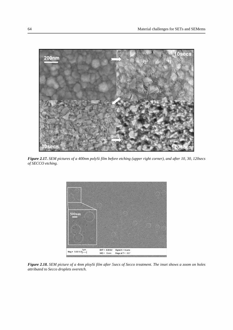
64 Material challenges for SETs and SEMems
Figure 2.17. SEM pictures of a 400nm polySi film before etching (upper right corner), and after 10, 30, 120secsof SECCO etching.
Figure 2.18. SEM picture of a 4nm ploySi film after 5secs of Secco treatment. The inset shows a zoom on holesattributed to Secco droplets overetch.
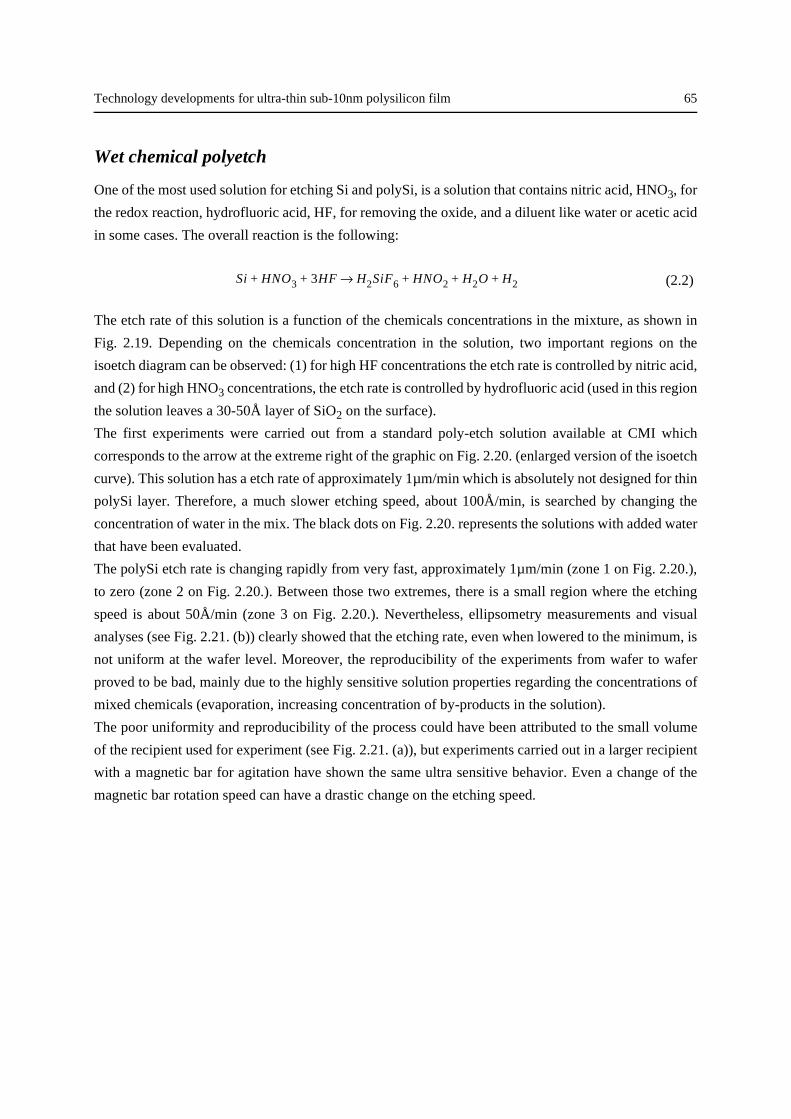
Technology developments for ultra-thin sub-10nm polysilicon film 65
Wet chemical polyetch
One of the most used solution for etching Si and polySi, is a solution that contains nitric acid, HNO3, for
the redox reaction, hydrofluoric acid, HF, for removing the oxide, and a diluent like water or acetic acid
in some cases. The overall reaction is the following:
(2.2)
The etch rate of this solution is a function of the chemicals concentrations in the mixture, as shown in
Fig. 2.19. Depending on the chemicals concentration in the solution, two important regions on the
isoetch diagram can be observed: (1) for high HF concentrations the etch rate is controlled by nitric acid,
and (2) for high HNO3 concentrations, the etch rate is controlled by hydrofluoric acid (used in this region
the solution leaves a 30-50Å layer of SiO2 on the surface).
The first experiments were carried out from a standard poly-etch solution available at CMI which
corresponds to the arrow at the extreme right of the graphic on Fig. 2.20. (enlarged version of the isoetch
curve). This solution has a etch rate of approximately 1µm/min which is absolutely not designed for thin
polySi layer. Therefore, a much slower etching speed, about 100Å/min, is searched by changing the
concentration of water in the mix. The black dots on Fig. 2.20. represents the solutions with added water
that have been evaluated.
The polySi etch rate is changing rapidly from very fast, approximately 1µm/min (zone 1 on Fig. 2.20.),
to zero (zone 2 on Fig. 2.20.). Between those two extremes, there is a small region where the etching
speed is about 50Å/min (zone 3 on Fig. 2.20.). Nevertheless, ellipsometry measurements and visual
analyses (see Fig. 2.21. (b)) clearly showed that the etching rate, even when lowered to the minimum, is
not uniform at the wafer level. Moreover, the reproducibility of the experiments from wafer to wafer
proved to be bad, mainly due to the highly sensitive solution properties regarding the concentrations of
mixed chemicals (evaporation, increasing concentration of by-products in the solution).
The poor uniformity and reproducibility of the process could have been attributed to the small volume
of the recipient used for experiment (see Fig. 2.21. (a)), but experiments carried out in a larger recipient
with a magnetic bar for agitation have shown the same ultra sensitive behavior. Even a change of the
magnetic bar rotation speed can have a drastic change on the etching speed.
Si HNO3 3HF+ + H2SiF6 HNO2 H2O H2+ + +→
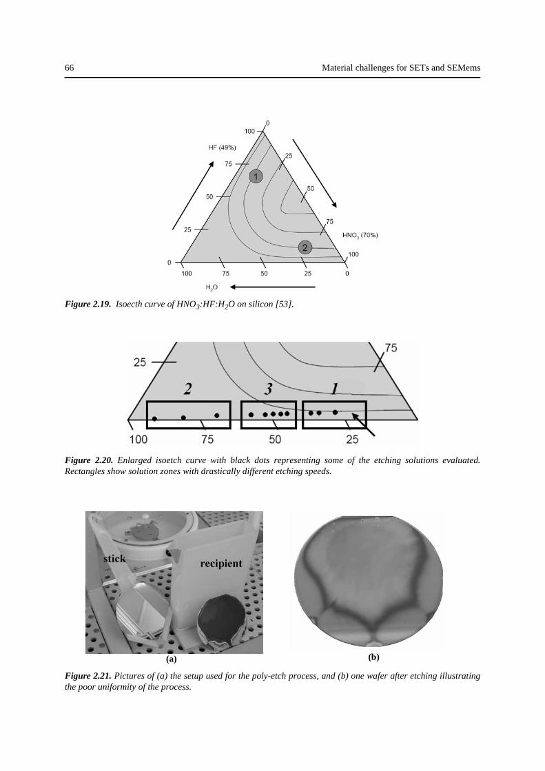
66 Material challenges for SETs and SEMems
Figure 2.19. Isoecth curve of HNO3:HF:H2O on silicon [53].
Figure 2.20. Enlarged isoetch curve with black dots representing some of the etching solutions evaluated.Rectangles show solution zones with drastically different etching speeds.
Figure 2.21. Pictures of (a) the setup used for the poly-etch process, and (b) one wafer after etching illustratingthe poor uniformity of the process.
(a) (b)
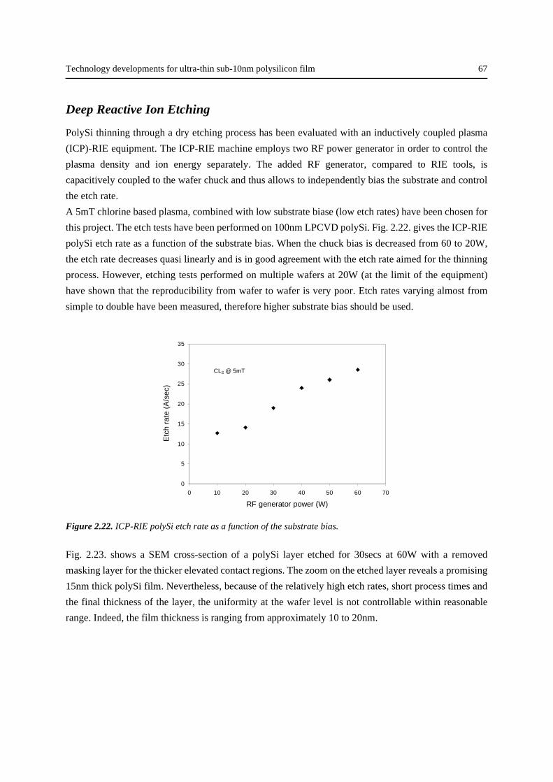
Technology developments for ultra-thin sub-10nm polysilicon film 67
Deep Reactive Ion Etching
PolySi thinning through a dry etching process has been evaluated with an inductively coupled plasma
(ICP)-RIE equipment. The ICP-RIE machine employs two RF power generator in order to control the
plasma density and ion energy separately. The added RF generator, compared to RIE tools, is
capacitively coupled to the wafer chuck and thus allows to independently bias the substrate and control
the etch rate.
A 5mT chlorine based plasma, combined with low substrate biase (low etch rates) have been chosen for
this project. The etch tests have been performed on 100nm LPCVD polySi. Fig. 2.22. gives the ICP-RIE
polySi etch rate as a function of the substrate bias. When the chuck bias is decreased from 60 to 20W,
the etch rate decreases quasi linearly and is in good agreement with the etch rate aimed for the thinning
process. However, etching tests performed on multiple wafers at 20W (at the limit of the equipment)
have shown that the reproducibility from wafer to wafer is very poor. Etch rates varying almost from
simple to double have been measured, therefore higher substrate bias should be used.
Figure 2.22. ICP-RIE polySi etch rate as a function of the substrate bias.
Fig. 2.23. shows a SEM cross-section of a polySi layer etched for 30secs at 60W with a removed
masking layer for the thicker elevated contact regions. The zoom on the etched layer reveals a promising
15nm thick polySi film. Nevertheless, because of the relatively high etch rates, short process times and
the final thickness of the layer, the uniformity at the wafer level is not controllable within reasonable
range. Indeed, the film thickness is ranging from approximately 10 to 20nm.
0
5
10
15
20
25
30
35
0 10 20 30 40 50 60 70
RF generator power (W)
Etc
h ra
te (
A/s
ec)
CL2 @ 5mT
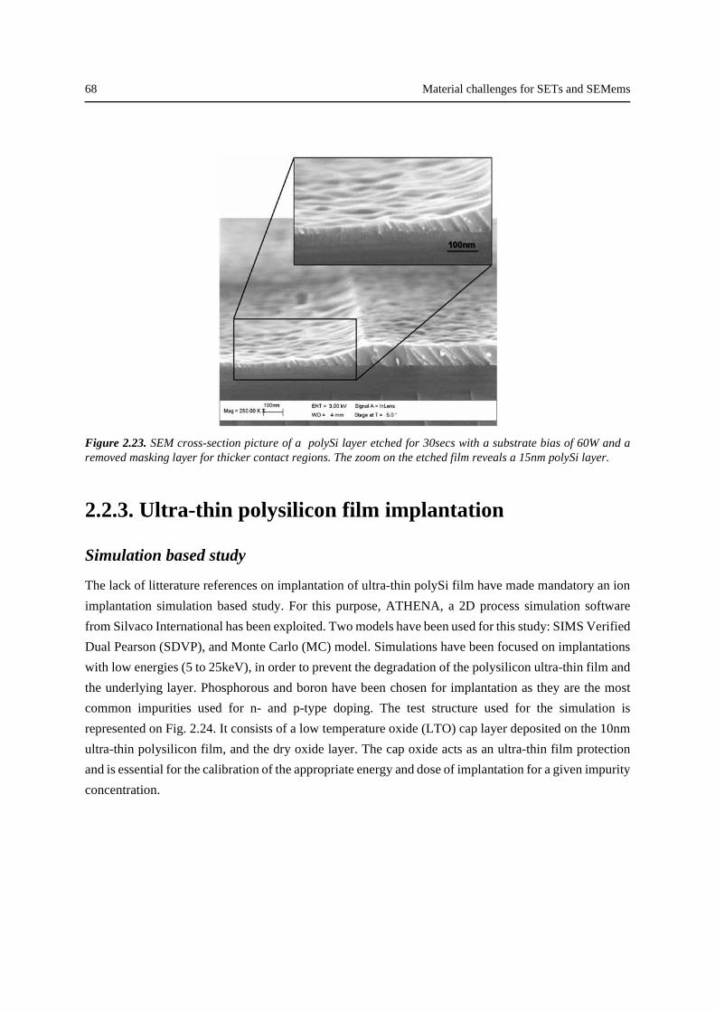
68 Material challenges for SETs and SEMems
Figure 2.23. SEM cross-section picture of a polySi layer etched for 30secs with a substrate bias of 60W and aremoved masking layer for thicker contact regions. The zoom on the etched film reveals a 15nm polySi layer.
2.2.3. Ultra-thin polysilicon film implantation
Simulation based study
The lack of litterature references on implantation of ultra-thin polySi film have made mandatory an ion
implantation simulation based study. For this purpose, ATHENA, a 2D process simulation software
from Silvaco International has been exploited. Two models have been used for this study: SIMS Verified
Dual Pearson (SDVP), and Monte Carlo (MC) model. Simulations have been focused on implantations
with low energies (5 to 25keV), in order to prevent the degradation of the polysilicon ultra-thin film and
the underlying layer. Phosphorous and boron have been chosen for implantation as they are the most
common impurities used for n- and p-type doping. The test structure used for the simulation is
represented on Fig. 2.24. It consists of a low temperature oxide (LTO) cap layer deposited on the 10nm
ultra-thin polysilicon film, and the dry oxide layer. The cap oxide acts as an ultra-thin film protection
and is essential for the calibration of the appropriate energy and dose of implantation for a given impurity
concentration.
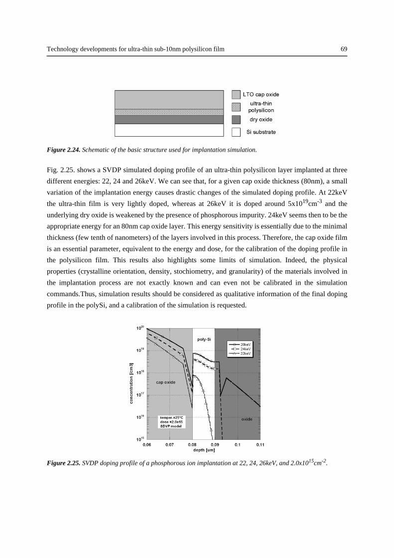
Technology developments for ultra-thin sub-10nm polysilicon film 69
Figure 2.24. Schematic of the basic structure used for implantation simulation.
Fig. 2.25. shows a SVDP simulated doping profile of an ultra-thin polysilicon layer implanted at three
different energies: 22, 24 and 26keV. We can see that, for a given cap oxide thickness (80nm), a small
variation of the implantation energy causes drastic changes of the simulated doping profile. At 22keV
the ultra-thin film is very lightly doped, whereas at 26keV it is doped around 5x1019cm-3 and the
underlying dry oxide is weakened by the presence of phosphorous impurity. 24keV seems then to be the
appropriate energy for an 80nm cap oxide layer. This energy sensitivity is essentially due to the minimal
thickness (few tenth of nanometers) of the layers involved in this process. Therefore, the cap oxide film
is an essential parameter, equivalent to the energy and dose, for the calibration of the doping profile in
the polysilicon film. This results also highlights some limits of simulation. Indeed, the physical
properties (crystalline orientation, density, stochiometry, and granularity) of the materials involved in
the implantation process are not exactly known and can even not be calibrated in the simulation
commands.Thus, simulation results should be considered as qualitative information of the final doping
profile in the polySi, and a calibration of the simulation is requested.
Figure 2.25. SVDP doping profile of a phosphorous ion implantation at 22, 24, 26keV, and 2.0x1015cm-2.
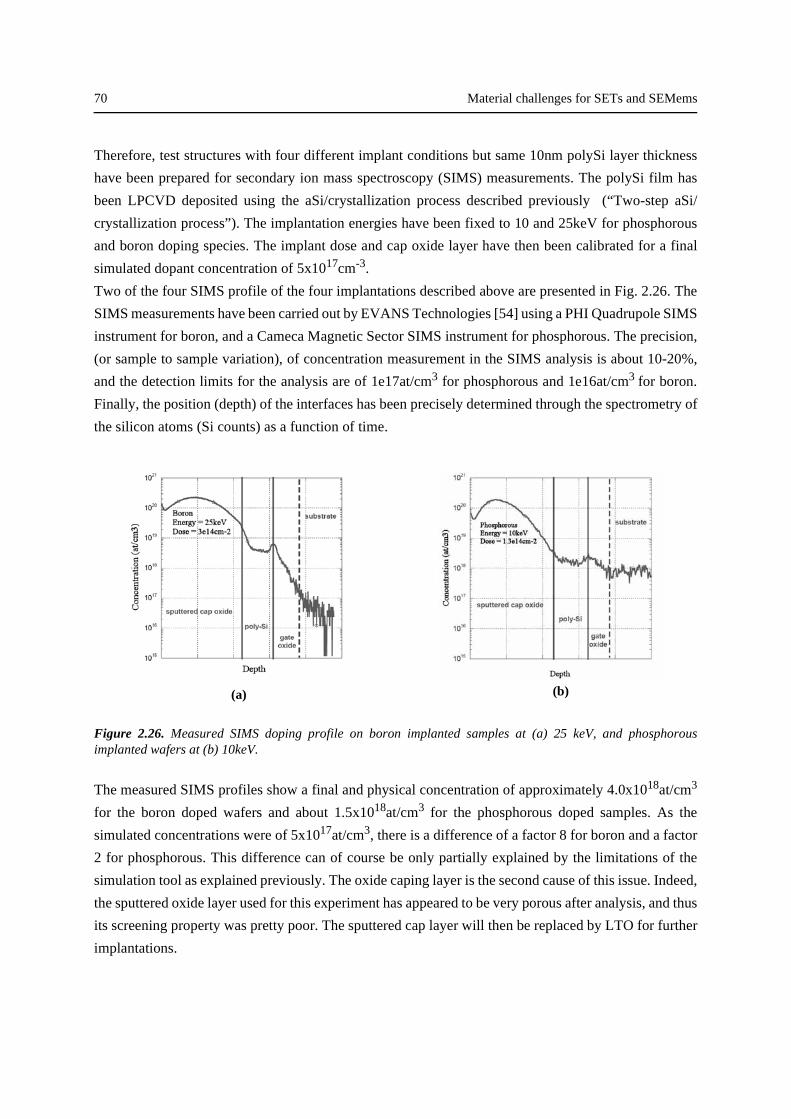
70 Material challenges for SETs and SEMems
Therefore, test structures with four different implant conditions but same 10nm polySi layer thickness
have been prepared for secondary ion mass spectroscopy (SIMS) measurements. The polySi film has
been LPCVD deposited using the aSi/crystallization process described previously (“Two-step aSi/
crystallization process”). The implantation energies have been fixed to 10 and 25keV for phosphorous
and boron doping species. The implant dose and cap oxide layer have then been calibrated for a final
simulated dopant concentration of 5x1017cm-3.
Two of the four SIMS profile of the four implantations described above are presented in Fig. 2.26. The
SIMS measurements have been carried out by EVANS Technologies [54] using a PHI Quadrupole SIMS
instrument for boron, and a Cameca Magnetic Sector SIMS instrument for phosphorous. The precision,
(or sample to sample variation), of concentration measurement in the SIMS analysis is about 10-20%,
and the detection limits for the analysis are of 1e17at/cm3 for phosphorous and 1e16at/cm3 for boron.
Finally, the position (depth) of the interfaces has been precisely determined through the spectrometry of
the silicon atoms (Si counts) as a function of time.
Figure 2.26. Measured SIMS doping profile on boron implanted samples at (a) 25 keV, and phosphorousimplanted wafers at (b) 10keV.
The measured SIMS profiles show a final and physical concentration of approximately 4.0x10¹⁸at/cm3
for the boron doped wafers and about 1.5x10¹⁸at/cm3 for the phosphorous doped samples. As the
simulated concentrations were of 5x10¹⁷at/cm3, there is a difference of a factor 8 for boron and a factor
2 for phosphorous. This difference can of course be only partially explained by the limitations of the
simulation tool as explained previously. The oxide caping layer is the second cause of this issue. Indeed,
the sputtered oxide layer used for this experiment has appeared to be very porous after analysis, and thus
its screening property was pretty poor. The sputtered cap layer will then be replaced by LTO for further
implantations.
(a) (b)
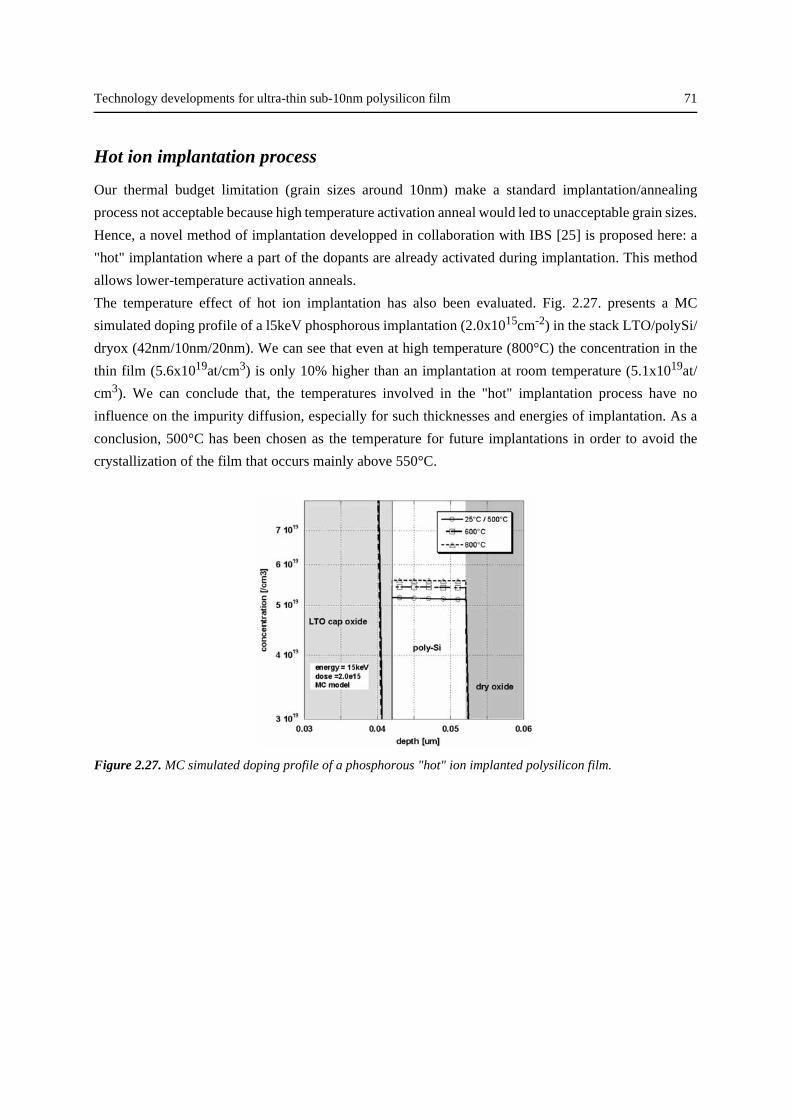
Technology developments for ultra-thin sub-10nm polysilicon film 71
Hot ion implantation process
Our thermal budget limitation (grain sizes around 10nm) make a standard implantation/annealing
process not acceptable because high temperature activation anneal would led to unacceptable grain sizes.
Hence, a novel method of implantation developped in collaboration with IBS [25] is proposed here: a
"hot" implantation where a part of the dopants are already activated during implantation. This method
allows lower-temperature activation anneals.
The temperature effect of hot ion implantation has also been evaluated. Fig. 2.27. presents a MC
simulated doping profile of a l5keV phosphorous implantation (2.0x1015cm-2) in the stack LTO/polySi/
dryox (42nm/10nm/20nm). We can see that even at high temperature (800°C) the concentration in the
thin film (5.6x10¹⁹at/cm3) is only 10% higher than an implantation at room temperature (5.1x10¹⁹at/
cm3). We can conclude that, the temperatures involved in the "hot" implantation process have no
influence on the impurity diffusion, especially for such thicknesses and energies of implantation. As a
conclusion, 500°C has been chosen as the temperature for future implantations in order to avoid the
crystallization of the film that occurs mainly above 550°C.
Figure 2.27. MC simulated doping profile of a phosphorous "hot" ion implanted polysilicon film.
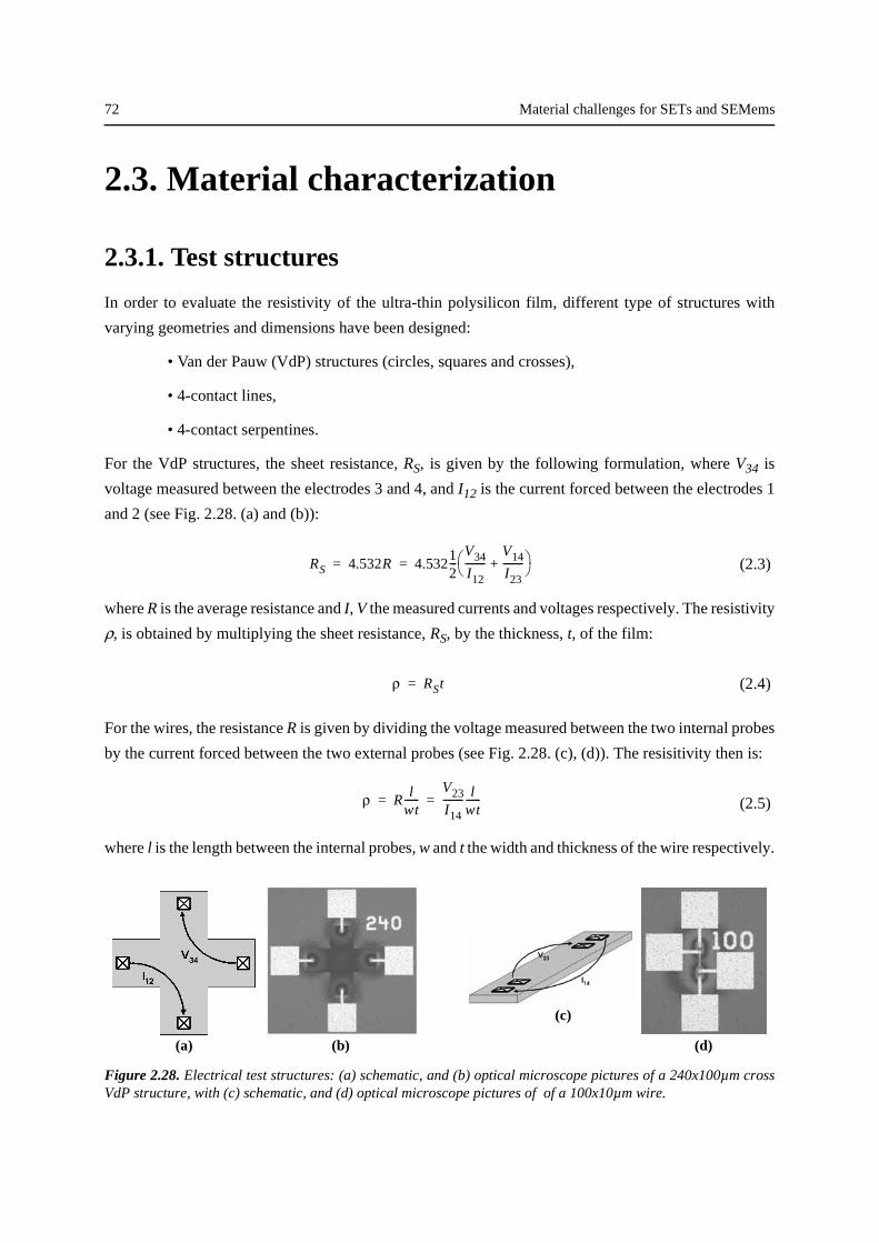
72 Material challenges for SETs and SEMems
2.3. Material characterization
2.3.1. Test structures
In order to evaluate the resistivity of the ultra-thin polysilicon film, different type of structures with
varying geometries and dimensions have been designed:
• Van der Pauw (VdP) structures (circles, squares and crosses),
• 4-contact lines,
• 4-contact serpentines.
For the VdP structures, the sheet resistance, RS, is given by the following formulation, where V34 is
voltage measured between the electrodes 3 and 4, and I12 is the current forced between the electrodes 1
and 2 (see Fig. 2.28. (a) and (b)):
(2.3)
where R is the average resistance and I, V the measured currents and voltages respectively. The resistivity
ρ, is obtained by multiplying the sheet resistance, RS, by the thickness, t, of the film:
(2.4)
For the wires, the resistance R is given by dividing the voltage measured between the two internal probes
by the current forced between the two external probes (see Fig. 2.28. (c), (d)). The resisitivity then is:
(2.5)
where l is the length between the internal probes, w and t the width and thickness of the wire respectively.
Figure 2.28. Electrical test structures: (a) schematic, and (b) optical microscope pictures of a 240x100µm crossVdP structure, with (c) schematic, and (d) optical microscope pictures of of a 100x10µm wire.
RS 4.532R 4.53212---
V34
I12--------
V14
I23--------+⎝ ⎠
⎛ ⎞= =
ρ RSt=
ρ Rl
wt------
V23
I14-------- l
wt------= =
(a) (b)
(c)
(d)
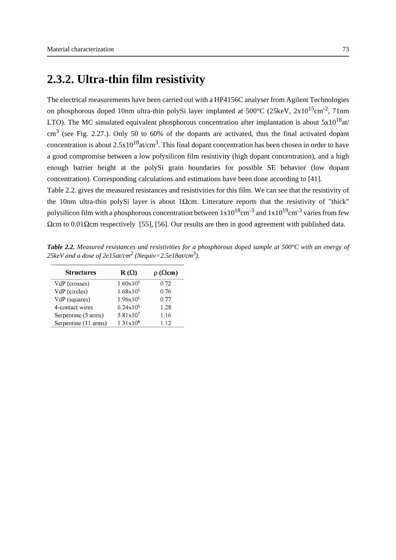
Material characterization 73
2.3.2. Ultra-thin film resistivity
The electrical measurements have been carried out with a HP4156C analyser from Agilent Technologies
on phosphorous doped 10nm ultra-thin polySi layer implanted at 500°C (25keV, 2x1015cm-2, 71nm
LTO). The MC simulated equivalent phosphorous concentration after implantation is about 5x10¹⁸at/
cm3 (see Fig. 2.27.). Only 50 to 60% of the dopants are activated, thus the final activated dopant
concentration is about 2.5x10¹⁸at/cm3. This final dopant concentration has been chosen in order to have
a good compromise between a low polysilicon film resistivity (high dopant concentration), and a high
enough barrier height at the polySi grain boundaries for possible SE behavior (low dopant
concentration). Corresponding calculations and estimations have been done according to [41].
Table 2.2. gives the measured resistances and resistivities for this film. We can see that the resistivity of
the 10nm ultra-thin polySi layer is about 1Ωcm. Litterature reports that the resistivity of "thick"
polysilicon film with a phosphorous concentration between 1x1018cm-3 and 1x1019cm-3 varies from few
Ωcm to 0.01Ωcm respectively [55], [56]. Our results are then in good agreement with published data.
Table 2.2. Measured resistances and resistivities for a phosphorous doped sample at 500°C with an energy of25keV and a dose of 2e15at/cm2 (Nequiv=2.5e18at/cm3).
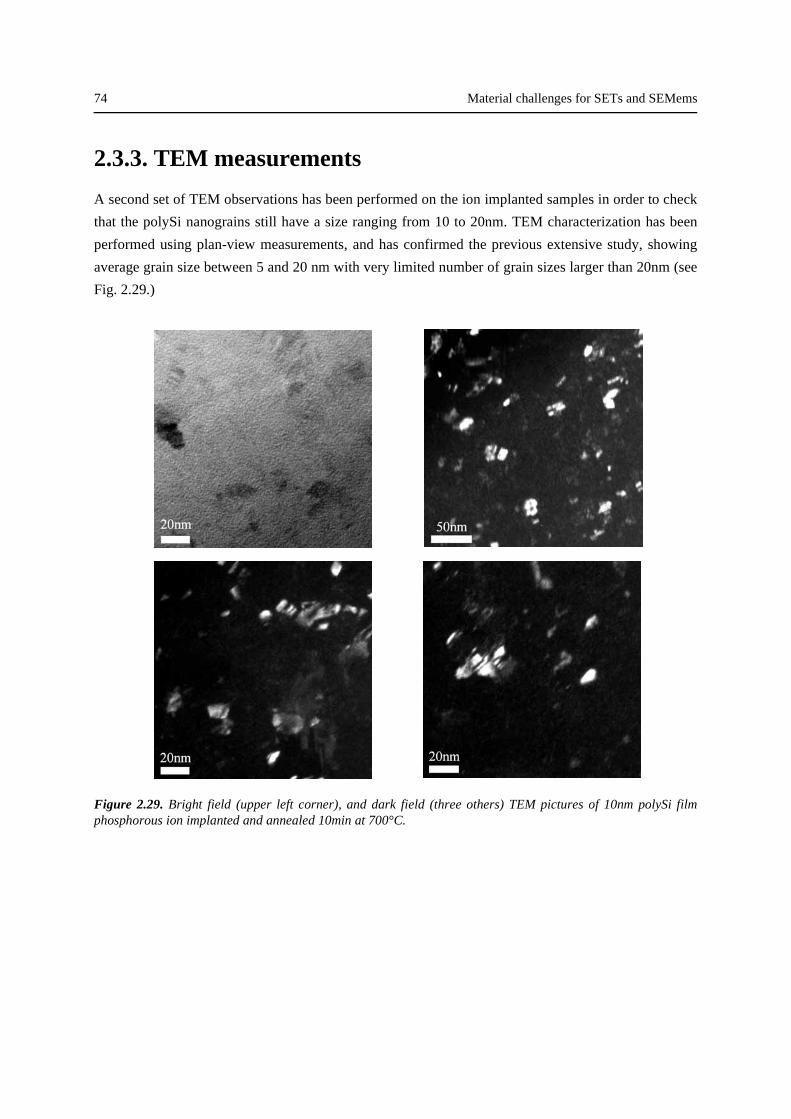
74 Material challenges for SETs and SEMems
2.3.3. TEM measurements
A second set of TEM observations has been performed on the ion implanted samples in order to check
that the polySi nanograins still have a size ranging from 10 to 20nm. TEM characterization has been
performed using plan-view measurements, and has confirmed the previous extensive study, showing
average grain size between 5 and 20 nm with very limited number of grain sizes larger than 20nm (see
Fig. 2.29.)
Figure 2.29. Bright field (upper left corner), and dark field (three others) TEM pictures of 10nm polySi filmphosphorous ion implanted and annealed 10min at 700°C.
Summary 75
2.4. Summary
A brief description of the materials available for single electronics (metals, molecules, CNTs, Si) has
been given at the beginning of this chapter. After having detailled the different methods to achieve
quantum confinement in silicon, we have focused our discussion on multi-island devices made out of
polySi which is the material used in this work.
Technological processes for the realization of ultra-thin nanograin polySi film have been described and
experimentally explored. Two different approaches, that are a direct LPCVD deposition or a thinning
method (dry or wet etching) have been more precisely developped. With a deposition of aSi at 500°C
followed by a crystallization anneal, we have obtained uniform polySi film as thin as 6nm with grain
sizes ranging from 5 to 20nm. The other deposition processes have lead to porous layers and/or grain
sizes between 10 to 50nm (HSG). Thinning methods show very poor uniformity at the wafer level and
are too hard to control for less than 10nm final thicknesses. The sacrificial oxidation process has shown
promising results (5nm thick polySi film), however due to the increase of grain sizes after oxidation
(100nm to 200nm), its use was considered prohibitive for obtaining a nanograin material. Finally, the
most adapted process has been considered as the two-step aSi deposition followed by crystallization
anneal.
A simulation based study has then been carried out in order to define the most adequate way of doping
a 10nm polySi film. The result of this study combined with SIMS measurements have shown that: (i) the
use of an LTO sacrifical cap oxide layer is mandatory before implantation, (ii) an ion implantation
performed at 500°C would be the most adequate technique if one wants to keep the grain sizes around
10nm and also have the dopants activated, and (iii) due to the extremely small thicknesses involved in
simulations, the predicted doping concentration should be rather considered as an order of magnitude
and not as an absolute value.
Original contributions
At our best knowledge, no precise description of the deposition and implantation techniques for SE ultra-
thin nanograin polySi film have been published before this work. Final results in terms of film thickness
were generally reported by other authors without any technological details. Here we have presented an
original process combining aSi deposition together with a novel hot ion implantation technique followed
by crystallization anneal. Using this process we have been able to fabricate doped polySi layers with
thicknesses less than 10nm, in which the grain sizes are controlled between 5 to 20nm.

76 Material challenges for SETs and SEMems
References 77
2.5. References
[1] T. A. Fulton, and G. J. Dolan, "Observation of Single-Electron Charging Effects in Small TunnelJunctions", Physical Review Letters, vol. 59 (1), pp. 109-113, 1987.
[2] D. Born, T. Wagner, W. Krech, U. Hübner, and L. Fritzch, "Fabrication of Ultrasmall Tunnel Junctions byElectron Beam Direct-Writing", IEEE Transactions on Applied Superconductivity, vol. 11 (1), pp. 373-376,2001.
[3] K. Matsumoto, M. Ishii, K. Segawa, Y. Oka, B. J. Vartanian, and S. J. Harris, "Room temperature operationof a single electron transistor made by the scanning tunneling microscope nanooxidation process for theTiOx/Ti system", Applied Physics Letters, vol. 68 (1), pp. 34-36, 1996.
[4] D. L. Klein, R. Roth, A. K. L. Lim, A. P. Alivisatos, and P. L. Mc Euen, "A single-electron transistor madefrom a cadmium selenide nanocrystal", Nature, vol. 389, pp. 699-701, 1997.
[5] S. Kubatkin, A. Danilov, M. Hjort, J. Cornil, J.-L. Brédas, N. Stuhr-Hansen, P. Hedegard, and T.Bjornholm, "Single-electron transistor of a single organic molecule with access to several redox states",Nature, vol. 425, pp. 6698-701, 2003.
[6] J. Park, A. N. Pasupathy, J. I. Goldsmith, C. Chang, Y. Yaish, J. R. Petta, M. Rinkoski, J. P. Sethna, H. D.Abruna, P. L. Mc Euen, and D. C. Ralph, "Coulomb blocakde and the Kondo effect in single-atomtransistors", Nature, vol. 417, pp. 722-725, 2002.
[7] Available online at http://en.wikipedia.org/wiki/Carbon
[8] Y. Kurokawa, Y. Ohno, S. Kishimoto, T. Okazaki, H. Shinohara, and T. Mizutani, "Fabrication Techniquefor Carbon Nanotube Single-Electron Transistors Using Focused Ion Beam", Japanese Journal of AppliedPhysics, vol. 43 (8A), pp. 5669-5670, 2004.
[9] H. W. C. Postma, T. Teepen, Z. Yao, M. Grifoni, and C. Dekker, "Carbon Nanotube Single-ElectronTransistos at Room Temperature", Science, vol. 293, pp. 76-79, 2001.
[10] K. Matsumoto, S. Kinoshita, Y. Gotoh, K. Kurachi, T. Kamimura, M. Maeda, K. Sakamoto, M. Kuwahara,N. Atoda, and Y. Awano, "Single-Electron Transistor with Ultra-High Coulomb Energy of 5000K UsingPosition Controlled Grown Carbon Nanotube as Channel", Japanese Journal of Applied Physics, vol. 42(4B), pp. 2415-2418, 2004.
[11] Y. Takahashi, Y. Ono, A. Fujiwara, and H. Inokawa, "Silicon Single-Electron Devices", NTT Review, vol.2 (2), pp. 21-27, 2004.
[12] Y. Ono, Y. Takahashi, K. Yamazaki, M. Nagase, H. Namatsu, K. Kurihara, and K. Murase, "FabricationMethod for IC-Oriented Si Single-Electron Transistors", IEEE Transactions on Nanotechnology, vol. 47(1), pp. 147-153, 2000.
[13] L. Zhuang, L. Guo, and S. Y. Chou, "Silicon single-electron quantum-dot transistor switch operating atroom temperature", Applied Physics Letters, vol. 72 (10), pp. 1205-1207, 1998.
[14] K. Yano, T. Ishii, T. Sano, T. Mine, F. Murai, T. Hashimoto, T. Kobayashi, T. Kure, and K. Seki, "Single-Electron Memory for Giga-to-Tera Bit Storage", Proceedings of the IEEE, vol. 87 (4), pp. 633-601, 1999.
[15] A. Dutta, S. P. Lee, Y. Hayafune, S. Hatatani, and S. Oda, "Single-Electron Tunneling Devices Based onSilicon Quantum Dots Fabricated by Plasma Process", Japanese Journal of Applied Physics, vol. 39 (1), pp.264-267, 2000.
[16] K. Uchida, J. Koga, R. Ohba, S. Takagi, and A. Toriumi, "Silicon single-electron tunneling devicefabricated in an undulated ultrathin silicon-on-insulator film", Journal of Applied Physics, vol. 90 (7), pp.3551-3557, 2001.
[17] Y. Ito, T. Hatano, A. Nakajima, and S. Yokoyama, "Fabrication of Si single-electron transistors havingdouble SiO2 barriers", Applied Physics Letters, vol. 80 (24), pp. 4617-4619, 2002.
[18] T. Koester, F. Goldschmidtboeing, B. Hadam, J. Stein, S. Altmeyer, B. Spangenberg, H. Kurz, R. Neumann,K. Brunner, and G. Abstreiter, "Coulomnb Blockade Effects in a Highly Doped Silicon quantum WireFabricated on Novel Molecular Beam Epitaxy Grown Material", Japanese Journal of Applied Physics, vol.38 (1), pp. 465-468, 1999.
[19] M. Specht, M. Sanquer, C. Caillat, G. Guegan, and S. Deleonibus, "Coulomb Oscillations in 100nm and50nm CMOS Devices", Technical Digest of the International Electron Devices Meeting IEDM 1999, pp.383-385, 1999.
78 Material challenges for SETs and SEMems
[20] D. H. Kim, S.-K. Sung, K. R. Kim, J. D. Lee, and B.-G. Park, "Fabrication of single-electron tunnelingtransistors with an electrically formed Coulomb island in a silicon-on-insulator nanowire", Journal ofVacuum Science and Technology B, vol. 20 (4), pp. 1410-1418, 2002.
[21] F. Boeuf, X. Jehl, M. Sanquer, and T. Skotnicki, "Controlled Single-Electron Effects in NonoverlappedUltra-Short Silicon Field Effect Transistors", IEEE Transactions on Nanotechnology, vol. 2 (3), pp. 144-148, 2003.
[22] F. Boeuf, T. Skotnicki, S. Monfray, C. Julien, D. Dutartre, J. Martins, P. Mazoyer, R. Palla, B. Tavel, P.Ribot, E. Sondergard, and M. Sanquer, "16nm planar NMOSFET manufacturable within state-of-the-artCMOS process thanks to specific design and optimisation", Technical Digest of the International ElectronDevices Meeting IEDM 2001, pp. 637-640, 2001.
[23] K. Kawamura, T. Kidera, A. Nakajima, and S. Yokoyama, "Coulomb blockade effects and conductionmechanism in extremely thin polycrystalline-silicon wires", Journal of Applied Physics, vol. 91 (8), pp.5213-5220, 2002.
[24] A. H. M. Kamal, J. Lützen, B. A. Sanborn, M. V. Sidorov, M. N. Kozicki, D. J. Smith, and D. K. Ferry, "Atwo-terminal nanocrystalline silicon memory device at room temperature", Semiconductor Science andTechnology, vol. 13, pp. 1328-1332, 1998.
[25] Ion Beam Services, IBS, www.ion-beam-services.com.
[26] M. Ino, J. Miyano, H. Kurogi, H. Tamura, Y. Nagatomo, and M. Yoshimura, "Rugged surfacepolycrystalline silicon film deposition and its application in a stacked dynamic random access memorycapacitor electrode", Journal of Vacuum Science and Technology B, vol. 14 (2), pp. 751-756, 1996.
[27] Y. T. Kim, H. J. Yoo, C. H. Jun, W. I. Jang, and S. H. Kim, "Activation and recrystalliutaion of ion-implanted amorphous silicon films by rapid thermal annealing", Journal of Vacuum Science andTechnology A, vol. 7 (3), pp. 796-801, 1989.
[28] M. Reiche, and S. Hopfe, "TEM IN-SITU INVESTIGATIONS OF THE CRYSTALLIZATIONBEHAVIOUR OF AMORPHOUS SILICON THIN FILMS", Ultramicroscopy, vol. 33, pp. 41-50, 1990.
[29] M. K. Hatalis, and D. W. Greve, "Large grain polycrystalline silicon by low temperature annealing of low-pressure chemical vapor deposited amorphous silicon films", Journal of Applied Physics, vol. 63 (7), pp.2260-2266, 1988.
[30] E. G. Lee, and J. J. Kim, "Investigation of microstructure and grain growth of polycrystalline silicondeposited using silane and disilane", Thin Solid Films, vol. 226, pp. 123-128, 1993.
[31] T. Mohammed-Brahim, M. Sarret, D. Briand, K. Kis-Sion, O. Bonnaud, and A. Hadjaj, "PolycrystallineSilicon Characteristics Dependence on Starting Amorphous Material", Journal de Physique IV, C5, pp. 913-920, 1995.
[32] A. G. Nassiopoulou, V. Ioannou-Sougleridis, P. Photopoulos, A. Travlos, V. Tsakiri, and D. Papadimitriou,"Stable Visible Photo- and Electroluminescence from Nanocrystalline Silicon Thin Films Fabricated onThin SiO2 Layers by Low Pressure Chemical Vapour Deposition", Physica Status Solidi (a), vol. 165, pp.79-85, 1997.
[33] F. Bertin, T. Baron, D. Mariolle, F. Martin, A. Chabli, and M. Dupuy, "Characterization of DepositedNanocrystalline Silicon by Spectroscopic Ellipsometry", Physica Status Solidi (a), vol. 175, pp. 405-412,1999.
[34] T. Baron, F. Martin, P. Mur, C. Wyon, and M. Dupuy, "Silicon quantum dot nucleation on Si3N4, SiO2, andSiOxNy substrates for nanoelectronics devices", Journal of Crystal Growth, vol. 209, pp. 1004-1008, 2000.
[35] S. Miyazaki, Y. Hamamoto, E. Yoshida, M. Ikeda, and M. Hirose, "Control of self-assembling formationof nanometer silicon dots by low pressure chemical vapor deposition", Thin Solid Films, vol. 369, pp. 55-59, 2000.
[36] Y. Hirano, F. Sato, N. Saito, M. Abe, S. Miyazaki, and M. Hirose, "Fabrication of nanometer sized Si dotmultilayers and their photoluminescence properties", Journal of Non-Crystalline Solids, vol. 266-269, pp.1004-1008, 2000.
[37] E. Ibok, and S. Garg, "A characterization on the effect of deposition temperature on polysilicon properties",Journal of the Electrochemical Society, vol. 140 (10), pp. 2927-2937, 1993.
[38] L. Asinovsky, M. Schroth, F. Shen, and J. Sweeney, "Characterization and metrology of low pressurechemical vapor deposited polysilicon", Material Research Society Symposium proceedings, vol. 452, 1997.
[39] R. E. Mallard, D. C. Houghton, G. J. C. Carpenter, and F. R. Sheperd, "Morphology of LPCVDpolycrystalline Si", Institute of Physics Conference Series, vol. 76 (4), pp. 145-150, 1985.
References 79
[40] Center of Micro/Nanotecnology, http://cmi/thinfilms/Tube_1-1.htm.
[41] T. Kamins, "Polycrystalline Silicon for Integrated Circuit Applications", Kluwer Academic Publishers USA,1988.
[42] A. Sakai, T. Tatsumi, T. Niino, H. Ono, and K. Ishida, "Crystallization of amorphous silicon films withnative-oxide free surfaces", Denki Kagaku, vol. 59 (12), pp. 1043, 1991.
[43] J.-M. Sallese, A. Ils, D. Bouvet, and P. Fazan, "Modelling of the depletion of the amorphous-silicon surfaceduring hemispherical grained silicon formation", Journal of Applied Physics, vol. 88 (10), pp. 5751-5755,2000.
[44] H. Watanabe, T. Tatsumi, T. Ikarashi, A. Sakai, N. Aoto, and T. Nikawa, "An advanced technique forfabricating hemispherical-grained (HSG) silicon storage electrodes", IEEE Transactions on ElectronDevices, vol. 42 (2), pp. 295-300, 1995.
[45] G. J. Parker, J. M. Bonar, and C. M. K. Starbuck, "Long incubation times for selective epitaxial growth ofsilicon using silane only", IEEE Electronics Letters, vol. 27 (17), pp. 1595-1597, 1991.
[46] K. Uchida, J. Koga, R. Ohba, S. Takagi, and A. Toriumi, "Planar Non-Volatile Memory with Single-Electron Channel Fabricated on a Hyper-thin SOI Film", 57th Device Research Conference DRC 1999, pp.138-139, 1999.
[47] R. A. Levy, "Microelectronic Materials and Processes", Kluwer Academic Publishers, 1986.
[48] C. Y. Lu, and N. S. Tsai, "Thermal oxidation of UNdoped LPCVD Polycrystalline-Silicon Films", Journalof the Electrochemical Society, vol. 133, pp. 446-447, 1986.
[49] M. Nagase, S. Horiguchi, A. Fujiwara, Y. Ono, K. Yamazaki, H. Namatsu, and Y. Takahashi, "Single-electron devices formed by pattern-dependent oxidation: microscopic structural evaluation", AppliedSurface Sciences, vol. 190, pp. 144-150, 2002.
[50] F. S. d’Aragona, "Dislocation Etch for (100) Planes in Silicon", Journal of the Electrochemical Society:Solid-State Science and Technology, vol. 119, pp. 948-951, 1972.
[51] B. Rezek, C. E. Nebel, and M. Stutzmann, "Interference laser crystallization of microcrystalline siliconusing asymmetric beam intensities", Journal of Non-Crystalline Solids, vol. 266-269, pp. 650-653, 2000.
[52] D. G. Schimmel, "A Comparison of Chemical Etches for Revealing <100> Silicon Crystal Defects",Journal of the Electrochemical Society: Solid-State Science and Technology, vol. 123 (5), pp. 734-741,1976.
[53] Available online at: www.latech.edu/tech/engr/bme/gale_classes/mems/wetetchingred.pdf
[54] Cascade Scientific Ltd / Evans Europa, Uxbridge, Middlesex UB8 3PH, U.K.
[55] M. M. Mandurah, K. C. Saraswat, and T. I. Kamins, "Phosphorous doping of Loe Pressure ChemicallyVapor-Deposited Silicon Films", Journal of the Electrochemical Society: Solid-State Science andTechnology, vol. 126 (6), pp. 1019-1023, 1979.
[56] N. C.-C. Lu, L. Gerzberg, C.-Y. Lu, and J. D. Meindl, "A New Conduction Model for PolycrystallineSilicon Films", IEEE Electron Device Letters, vol. 2 (4), pp. 95-98, 1981.

80 Material challenges for SETs and SEMems
Fabrication 81
Chapter 3: Nanograinpolysilicon devices
In this chapter, the ion implantated ultra-thin nanograin polySi film is exploited for building pseudo-
MOSFET devices for possible SET or SEMem applications. The aim of the fabrication process is to use
the structured ultra-thin polySi film as the active part (channel) of the device, and try to demonstrate that,
due to the nanograin sizes and channel thickness, charge trapping and/or Coulomb effects are appearing
even at room temperature.
3.1. Fabrication
3.1.1. Design
Fig. 3.1. shows a 3D schematic of an ultra-thin polysilicon nanowire (polySiNW) device as it will be
ideally fabricated in the CMI clean room. It consists of a bottom gate device with a structured and
implanted nanograin polySi channel lying on a gate oxide and in between two highly doped polySi pads.
The two thick pads in the contact regions allows to preserve the underlying gate oxide when contacting
and serves as S/D, while the polySi channel is electrostatically controlled using a buried gate. The all
structure is a field effect transistor.
Two lithography techniques are available at CMI. A laser direct writing with a resolution of 0.8µm with
an alignement precision of 250nm, and an UV mask lithography with a resolution of 1.5µm and an
alignement precision of 500nm (both under optimal process conditions, first mask). Thus, contacts,
polySi pads, metal lines, and buried gate feature sizes are ranging from more than 1µm to 10 or 15µm.
The width, W, of the polySiNW will be reduced in some processes by sub-contracting 300nm deepUV
lithography to Vectron [1], while the polySiNW lenght, L, is defined by CMI lithography.
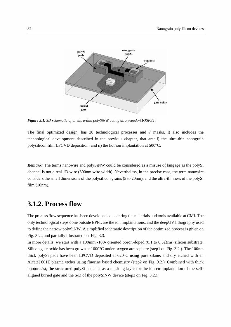
82 Nanograin polysilicon devices
Figure 3.1. 3D schematic of an ultra-thin polySiNW acting as a pseudo-MOSFET.
The final optimized design, has 38 technological processes and 7 masks. It also includes the
technological development described in the previous chapter, that are: i) the ultra-thin nanograin
polysilicon film LPCVD deposition; and ii) the hot ion implantation at 500°C.
Remark: The terms nanowire and polySiNW could be considered as a misuse of langage as the polySi
channel is not a real 1D wire (300nm wire width). Nevertheless, in the precise case, the term nanowire
considers the small dimensions of the polysilicon grains (5 to 20nm), and the ultra-thinness of the polySi
film (10nm).
3.1.2. Process flow
The process flow sequence has been developed considering the materials and tools available at CMI. The
only technological steps done outside EPFL are the ion implantations, and the deepUV lithography used
to define the narrow polySiNW. A simplified schematic description of the optimized process is given on
Fig. 3.2., and partially illustrated on Fig. 3.3.
In more details, we start with a 100mm ‹100› oriented boron-doped (0.1 to 0.5Ωcm) silicon substrate.
Silicon gate oxide has been grown at 1000°C under oxygen atmosphere (step1 on Fig. 3.2.). The 100nm
thick polySi pads have been LPCVD deposited at 620°C using pure silane, and dry etched with an
Alcatel 601E plasma etcher using fluorine based chemistry (step2 on Fig. 3.2.). Combined with thick
photoresist, the structured polySi pads act as a masking layer for the ion co-implantation of the self-
aligned buried gate and the S/D of the polySiNW device (step3 on Fig. 3.2.).
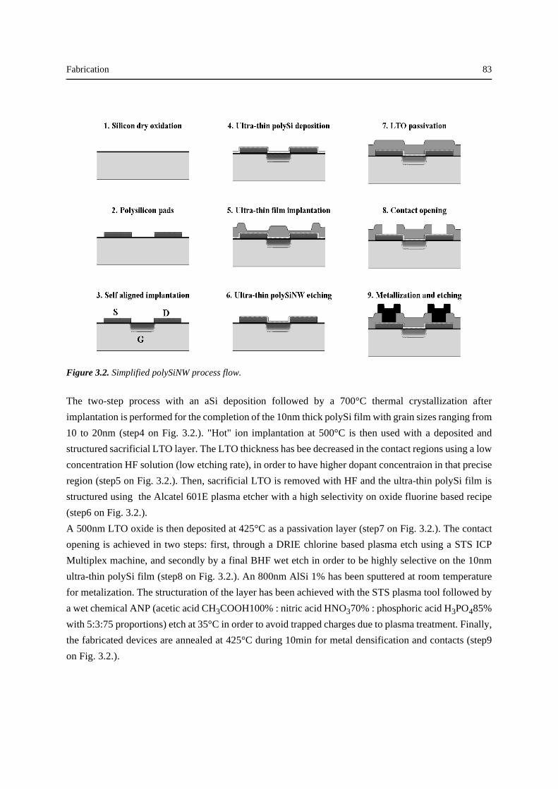
Fabrication 83
Figure 3.2. Simplified polySiNW process flow.
The two-step process with an aSi deposition followed by a 700°C thermal crystallization after
implantation is performed for the completion of the 10nm thick polySi film with grain sizes ranging from
10 to 20nm (step4 on Fig. 3.2.). "Hot" ion implantation at 500°C is then used with a deposited and
structured sacrificial LTO layer. The LTO thickness has bee decreased in the contact regions using a low
concentration HF solution (low etching rate), in order to have higher dopant concentraion in that precise
region (step5 on Fig. 3.2.). Then, sacrificial LTO is removed with HF and the ultra-thin polySi film is
structured using the Alcatel 601E plasma etcher with a high selectivity on oxide fluorine based recipe
(step6 on Fig. 3.2.).
A 500nm LTO oxide is then deposited at 425°C as a passivation layer (step7 on Fig. 3.2.). The contact
opening is achieved in two steps: first, through a DRIE chlorine based plasma etch using a STS ICP
Multiplex machine, and secondly by a final BHF wet etch in order to be highly selective on the 10nm
ultra-thin polySi film (step8 on Fig. 3.2.). An 800nm AlSi 1% has been sputtered at room temperature
for metalization. The structuration of the layer has been achieved with the STS plasma tool followed by
a wet chemical ANP (acetic acid CH3COOH100% : nitric acid HNO370% : phosphoric acid H3PO485%
with 5:3:75 proportions) etch at 35°C in order to avoid trapped charges due to plasma treatment. Finally,
the fabricated devices are annealed at 425°C during 10min for metal densification and contacts (step9
on Fig. 3.2.).
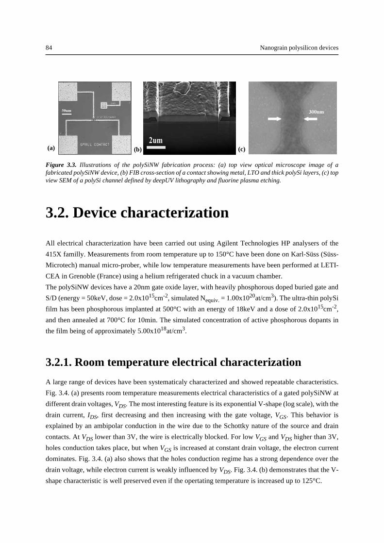
84 Nanograin polysilicon devices
Figure 3.3. Illustrations of the polySiNW fabrication process: (a) top view optical microscope image of afabricated polySiNW device, (b) FIB cross-section of a contact showing metal, LTO and thick polySi layers, (c) topview SEM of a polySi channel defined by deepUV lithography and fluorine plasma etching.
3.2. Device characterization
All electrical characterization have been carried out using Agilent Technologies HP analysers of the
415X familly. Measurements from room temperature up to 150°C have been done on Karl-Süss (Süss-
Microtech) manual micro-prober, while low temperature measurements have been performed at LETI-
CEA in Grenoble (France) using a helium refrigerated chuck in a vacuum chamber.
The polySiNW devices have a 20nm gate oxide layer, with heavily phosphorous doped buried gate and
S/D (energy = 50keV, dose = 2.0x1015cm-2, simulated Nequiv. = 1.00x10²⁰at/cm3). The ultra-thin polySi
film has been phosphorous implanted at 500°C with an energy of 18keV and a dose of 2.0x1015cm-2,
and then annealed at 700°C for 10min. The simulated concentration of active phosphorous dopants in
the film being of approximately 5.00x10¹⁸at/cm3.
3.2.1. Room temperature electrical characterization
A large range of devices have been systematicaly characterized and showed repeatable characteristics.
Fig. 3.4. (a) presents room temperature measurements electrical characteristics of a gated polySiNW at
different drain voltages, VDS. The most interesting feature is its exponential V-shape (log scale), with the
drain current, IDS, first decreasing and then increasing with the gate voltage, VGS. This behavior is
explained by an ambipolar conduction in the wire due to the Schottky nature of the source and drain
contacts. At VDS lower than 3V, the wire is electrically blocked. For low VGS and VDS higher than 3V,
holes conduction takes place, but when VGS is increased at constant drain voltage, the electron current
dominates. Fig. 3.4. (a) also shows that the holes conduction regime has a strong dependence over the
drain voltage, while electron current is weakly influenced by VDS. Fig. 3.4. (b) demonstrates that the V-
shape characteristic is well preserved even if the opertating temperature is increased up to 125°C.
(a) (b) (c)
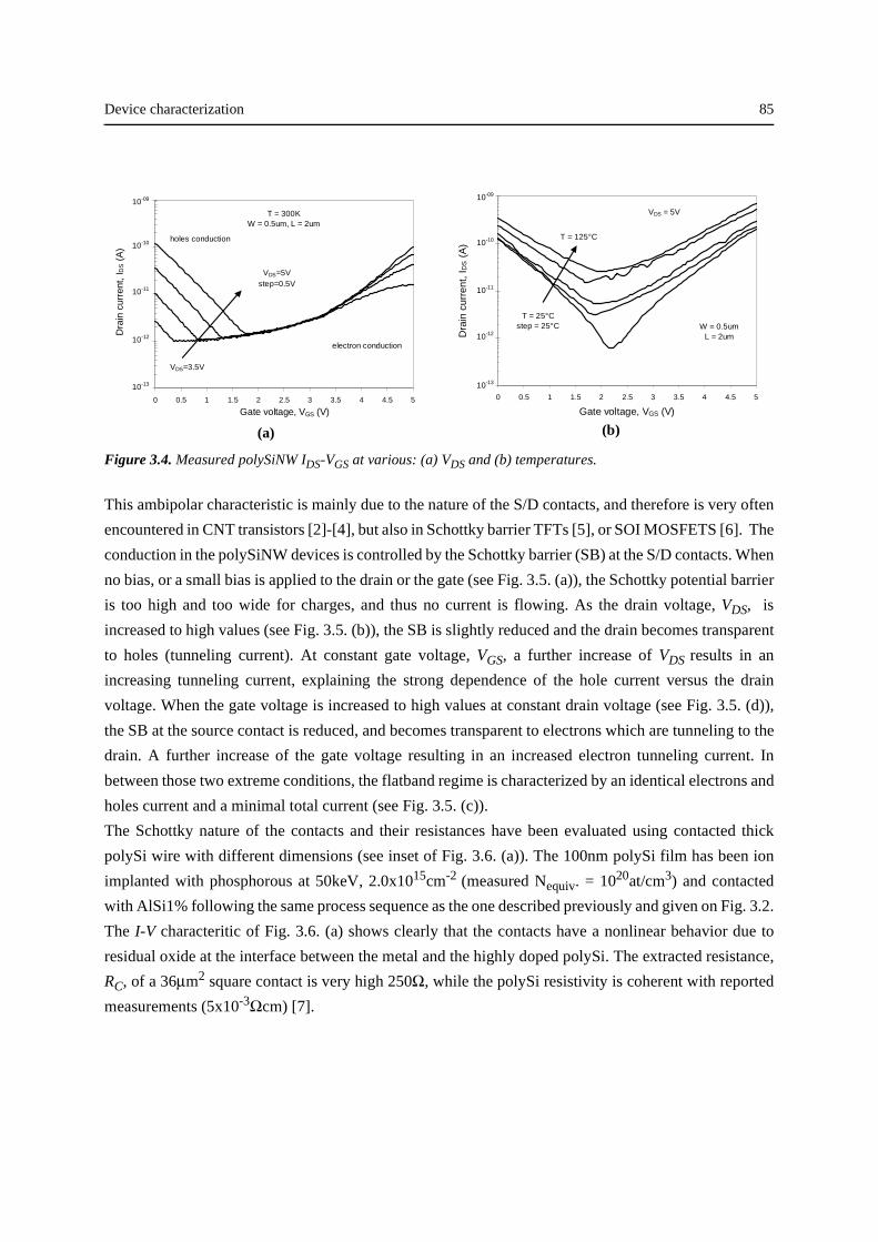
Device characterization 85
Figure 3.4. Measured polySiNW IDS-VGS at various: (a) VDS and (b) temperatures.
This ambipolar characteristic is mainly due to the nature of the S/D contacts, and therefore is very often
encountered in CNT transistors [2]-[4], but also in Schottky barrier TFTs [5], or SOI MOSFETS [6]. The
conduction in the polySiNW devices is controlled by the Schottky barrier (SB) at the S/D contacts. When
no bias, or a small bias is applied to the drain or the gate (see Fig. 3.5. (a)), the Schottky potential barrier
is too high and too wide for charges, and thus no current is flowing. As the drain voltage, VDS, is
increased to high values (see Fig. 3.5. (b)), the SB is slightly reduced and the drain becomes transparent
to holes (tunneling current). At constant gate voltage, VGS, a further increase of VDS results in an
increasing tunneling current, explaining the strong dependence of the hole current versus the drain
voltage. When the gate voltage is increased to high values at constant drain voltage (see Fig. 3.5. (d)),
the SB at the source contact is reduced, and becomes transparent to electrons which are tunneling to the
drain. A further increase of the gate voltage resulting in an increased electron tunneling current. In
between those two extreme conditions, the flatband regime is characterized by an identical electrons and
holes current and a minimal total current (see Fig. 3.5. (c)).
The Schottky nature of the contacts and their resistances have been evaluated using contacted thick
polySi wire with different dimensions (see inset of Fig. 3.6. (a)). The 100nm polySi film has been ion
implanted with phosphorous at 50keV, 2.0x1015cm-2 (measured Nequiv. = 1020at/cm3) and contacted
with AlSi1% following the same process sequence as the one described previously and given on Fig. 3.2.
The I-V characteritic of Fig. 3.6. (a) shows clearly that the contacts have a nonlinear behavior due to
residual oxide at the interface between the metal and the highly doped polySi. The extracted resistance,
RC, of a 36µm2 square contact is very high 250Ω, while the polySi resistivity is coherent with reported
measurements (5x10⁻³Ωcm) [7].
(a) (b)
0 0.5 1 1.5 2 2.5 3 3.5 4 4.5 5
Gate voltage, VGS (V)
Dra
in c
urre
nt, I
DS (
A)
10-13
10-12
10-11
10-10
10-09
T = 25°Cstep = 25°C
T = 125°C
VDS = 5V
W = 0.5umL = 2um
0 0.5 1 1.5 2 2.5 3 3.5 4 4.5 5
Gate voltage, VGS (V)
Dra
in c
urre
nt, I
DS (
A)
T = 300KW = 0.5um, L = 2um
VDS=3.5V
VDS=5Vstep=0.5V
holes conduction
electron conduction
10-09
10-13
10-12
10-11
10-10

86 Nanograin polysilicon devices
Figure 3.5. Band diagrams explaining the conduction in the polySiNW: (a) with no applied bias, (b) at high VDSand low VGS holes are tunneling from drain to source, (c) with increased VGS the electrons and holes current areidentical (flatband conditions), (d) and at high VDS and high VGS the current is dominated by electrons tunnelingfrom the source to the drain.
Fig. 3.6. (b) shows an I-V characteritic of a polySi wire before and after an oxide breakdown procedure
which demonstrates the presence of the oxide film. The oxide breakdown simply consisted in applying
a high voltage, typically 30V, between the two electrodes of the device after the first measurement. The
following I-V characteristic shows linear behavior and increased current. Finally, the presence of this
ultra-thin layer of oxide at the interface has been verified by high-resolution TEM and energy dispersive
X-ray (EDX) analysis.
Figure 3.6. I-V characteristics of thick (100nm) and large (10µm) phosphorous implanted polySi wireshighlighting the Schottky nature of the contacts: (a) I-V measurement with related total resistance, and (b) I-Vcharacteristic of a polySi wire before and after thin oxide breakdown.
(a) (b)
-3
-2
-1
0
1
2
3
-3 -2 -1 0 1 2 3
Bias (v)
Cur
rent
(m
A)
0
2
4
6
8
10
12
14
16
Res
ista
nce
(kO
hm)
-500
-300
-100
100
300
500
-2 -1.5 -1 -0.5 0 0.5 1 1.5 2
Bias (V)
Cur
rent
(µ
A)
before oxide breakdown
after oxide breakdown
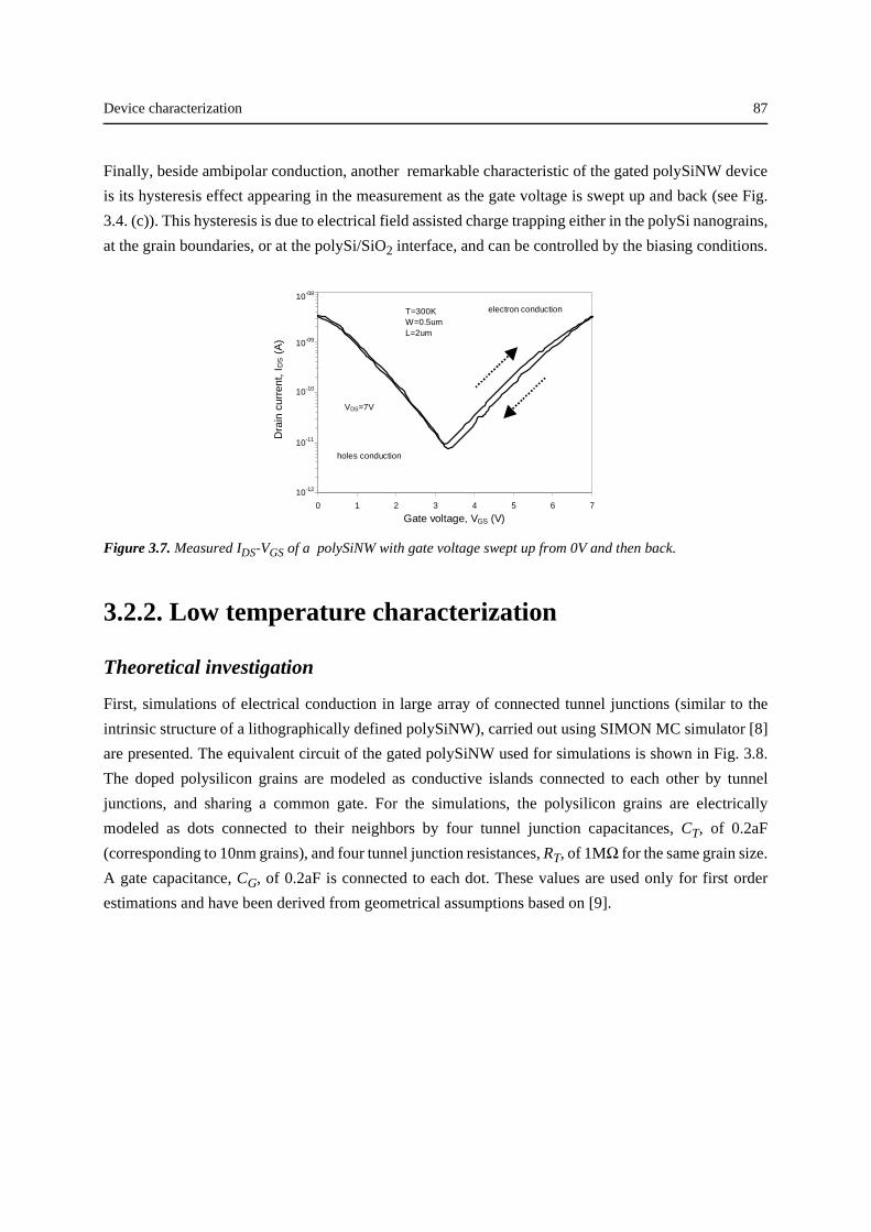
Device characterization 87
Finally, beside ambipolar conduction, another remarkable characteristic of the gated polySiNW device
is its hysteresis effect appearing in the measurement as the gate voltage is swept up and back (see Fig.
3.4. (c)). This hysteresis is due to electrical field assisted charge trapping either in the polySi nanograins,
at the grain boundaries, or at the polySi/SiO2 interface, and can be controlled by the biasing conditions.
Figure 3.7. Measured IDS-VGS of a polySiNW with gate voltage swept up from 0V and then back.
3.2.2. Low temperature characterization
Theoretical investigation
First, simulations of electrical conduction in large array of connected tunnel junctions (similar to the
intrinsic structure of a lithographically defined polySiNW), carried out using SIMON MC simulator [8]
are presented. The equivalent circuit of the gated polySiNW used for simulations is shown in Fig. 3.8.
The doped polysilicon grains are modeled as conductive islands connected to each other by tunnel
junctions, and sharing a common gate. For the simulations, the polysilicon grains are electrically
modeled as dots connected to their neighbors by four tunnel junction capacitances, CT, of 0.2aF
(corresponding to 10nm grains), and four tunnel junction resistances, RT, of 1MΩ for the same grain size.
A gate capacitance, CG, of 0.2aF is connected to each dot. These values are used only for first order
estimations and have been derived from geometrical assumptions based on [9].
0 1 2 3 4 5 6 7
Gate voltage, VGS (V)
Dra
in c
urre
nt, I
DS (
A)
VDS=7V
T=300KW=0.5umL=2um
holes conduction
electron conduction
10-08
10-12
10-11
10-10
10-09
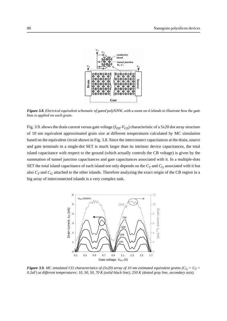
88 Nanograin polysilicon devices
Figure 3.8. Electrical equivalent schematic of gated polySiNW, with a zoom on 4 islands to illustrate how the gatebias is applied on each grain.
Fig. 3.9. shows the drain current versus gate voltage (IDS-VGS) characteristic of a 5x20 dot array structure
of 10 nm equivalent approximated grain size at different temperatures calculated by MC simulation
based on the equivalent circuit shown in Fig. 3.8. Since the interconnect capacitances at the drain, source
and gate terminals in a single-dot SET is much larger than its intrinsic device capacitances, the total
island capacitance with respect to the ground (which actually controls the CB voltage) is given by the
summation of tunnel junction capacitances and gate capacitances associated with it. In a multiple-dots
SET the total island capacitance of each island not only depends on the CT and CG associated with it but
also CT and CG attached to the other islands. Therefore analyzing the exact origin of the CB region in a
big array of interconnected islands is a very complex task.
Figure 3.9. MC simulated CO characteristics of (5x20) array of 10 nm estimated equivalent grains (CG = CT =0.2aF) at different temperatures: 10, 30, 50, 70 K (solid black line); 250 K (dotted gray line, secondary axis).
0
1
2
3
4
5
6
0.1 0.3 0.5 0.7 0.9 1.1 1.3 1.5 1.7
Gate voltage, VGS (V)
Dra
in c
urre
nt, I
DS (
nA)
0
2
4
6
8
10
12
Drain current, ID
S (nA)
VDS=200mV
250K
70K
50K
30K
10K
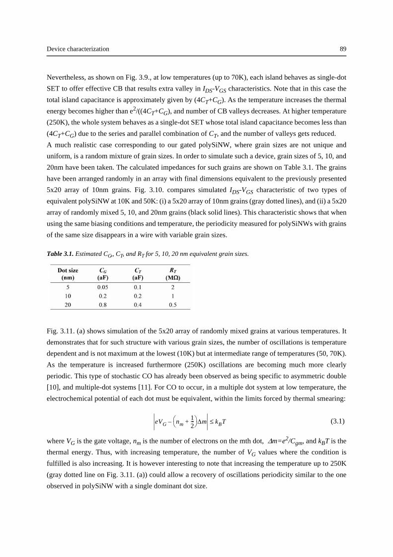
Device characterization 89
Nevertheless, as shown on Fig. 3.9., at low temperatures (up to 70K), each island behaves as single-dot
SET to offer effective CB that results extra valley in IDS-VGS characteristics. Note that in this case the
total island capacitance is approximately given by (4CT+CG). As the temperature increases the thermal
energy becomes higher than e2/((4CT+CG), and number of CB valleys decreases. At higher temperature
(250K), the whole system behaves as a single-dot SET whose total island capacitance becomes less than
(4CT+CG) due to the series and parallel combination of CT, and the number of valleys gets reduced.
A much realistic case corresponding to our gated polySiNW, where grain sizes are not unique and
uniform, is a random mixture of grain sizes. In order to simulate such a device, grain sizes of 5, 10, and
20nm have been taken. The calculated impedances for such grains are shown on Table 3.1. The grains
have been arranged randomly in an array with final dimensions equivalent to the previously presented
5x20 array of 10nm grains. Fig. 3.10. compares simulated IDS-VGS characteristic of two types of
equivalent polySiNW at 10K and 50K: (i) a 5x20 array of 10nm grains (gray dotted lines), and (ii) a 5x20
array of randomly mixed 5, 10, and 20nm grains (black solid lines). This characteristic shows that when
using the same biasing conditions and temperature, the periodicity measured for polySiNWs with grains
of the same size disappears in a wire with variable grain sizes.
Table 3.1. Estimated CG,, CT, and RT for 5, 10, 20 nm equivalent grain sizes.
Fig. 3.11. (a) shows simulation of the 5x20 array of randomly mixed grains at various temperatures. It
demonstrates that for such structure with various grain sizes, the number of oscillations is temperature
dependent and is not maximum at the lowest (10K) but at intermediate range of temperatures (50, 70K).
As the temperature is increased furthermore (250K) oscillations are becoming much more clearly
periodic. This type of stochastic CO has already been observed as being specific to asymmetric double
[10], and multiple-dot systems [11]. For CO to occur, in a multiple dot system at low temperature, the
electrochemical potential of each dot must be equivalent, within the limits forced by thermal smearing:
(3.1)
where VG is the gate voltage, nm is the number of electrons on the mth dot, ∆m=e2/Cgm, and kBT is the
thermal energy. Thus, with increasing temperature, the number of VG values where the condition is
fulfilled is also increasing. It is however interesting to note that increasing the temperature up to 250K
(gray dotted line on Fig. 3.11. (a)) could allow a recovery of oscillations periodicity similar to the one
observed in polySiNW with a single dominant dot size.
eVG nm12---+⎝ ⎠
⎛ ⎞∆m– kBT≤

90 Nanograin polysilicon devices
Figure 3.10. MC simulated CO characteristics of (5x20) array of (i) 10 nm (gray dotted line), and (ii) randomlymixed 5, 10, 20 nm (solid black line) estimated equivalent grains. See Table 3.1. for impedances values.
Figure 3.11. MC simulated CO characteristics of (5x20) array of randomly mixed 5, 10, 20nm estimatedequivalent grains at different: (a) temperatures, 10, 30, 50, 70K (solid black line), and 250K (dotted gray line,secondary axis), and (b) drain voltages, 50, 100, 150, 200 mV.
Wang et al [12], have demonstrated that stochastic COs in asymmetric structures are not only
temperature dependent but also drain voltage dependent. For an asymmetric double dot structure, the
number of stochastic COs are increasing with an increase of the drain voltage due to more effective non
resonant tunneling. This is confirmed on Fig. 3.11. (b) where an IDS-VGS characteristic is represented at
0.0
0.2
0.4
0.6
0.8
1.0
1.2
1.4
I DS (
nA)
10nm grains
mixed grains
0.0
0.5
1.0
1.5
2.0
2.5
3.0
0.1 0.3 0.5 0.7 0.9 1.1 1.3 1.5 1.7
VGS (V)
I DS (
nA)
T=50K VDS=200mV
T=10K VDS=200mV
(b)(a)
0.0
0.5
1.0
1.5
2.0
2.5
3.0
0.1 0.3 0.5 0.7 0.9 1.1 1.3 1.5 1.7
Gate voltage, VGS (V)
Dra
in c
urre
nt, I
DS (
nA)
T=50K
mixed grains
VDS = 200mV
50mV
0.0
0.5
1.0
1.5
2.0
2.5
3.0
3.5
4.0
4.5
5.0
0.1 0.3 0.5 0.7 0.9 1.1 1.3 1.5 1.7
Gate voltage, VGS (V)
Dra
in c
urre
nt, I
DS (
nA)
0
2
4
6
8
10
12
14
16
18
Drain current, ID
S (nA)
VDS = 200mV
T = 70K
50K
30K
10K
mixed grains
T = 250K
Device characterization 91
50K for four different drain voltages. The size and number of Coulomb peaks are maximum for 200mV
whereas at 50mV only four different peaks are visible. For drain voltages in-between intermediate
behavior is observed.
The results presented in this sub-chapter have shown that MC simulations (using SIMON software)
appear to be an adequate tool for the prediction of electrical behavior of multiple-dot systems connected
in arrays of tunnel junctions, like polysilicon. However, grain sizes, gate and tunnel capacitances, tunnel
resistances and dimensions have to be very well known or estimated, in order to have not only qualitative
but also accurate quantitative predictions.
Experimental investigation
Fig. 3.12. (a) presents measured IDS-VGS characteristic of a gated polySiNW at different temperatures
ranging from 300 to 50K, showing that the V-shape of the characteristics is fully preserved while the
current level is decreased. Fig. 3.12. (a) also shows that some oscillations become visible for
temperatures lower than 200K, especially for high values of VGS.
Fig. 3.12. (b) shows the conductance, G, versus the inverse of temperature extracted from measurements
at constant VDS and low temperatures, from 4.1 to 250K. For a fixed VGS two different thermally
activated conduction mechanisms are shown. Above 150K, conduction is dominated by thermally
activated hopping over the barrier at the polySi grain boundaries. The activation energy Ea1 related to
this mode of conduction is calculated by using the Arrehnius law [11] between conductance and
activation energy, Ea :
(3.2)
where k is the Boltzmann constant and T the temperature. Below 80K, the thermal carrier energy is too
low to turn on the hopping mechanism. At this range of temperature, the conduction is only controlled
by a thermally assisted tunneling process through the barrier with a second activation energy Ea2 of
~1.3meV. It is worth noting that the extraction of the activation energy has been carried out at VGS=4.5V,
in the electron conduction regime, where the SB to electrons at the contacts is reduced and its effect on
extraction less important.
GdIDS
dVGS------------- Ea
kT-------–⎝ ⎠
⎛ ⎞exp∝=
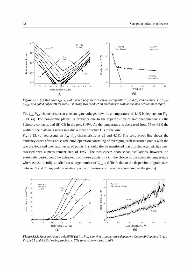
92 Nanograin polysilicon devices
Figure 3.12. (a) Measured IDS-VGS of a gated polySiNW at various temperatures, and (b) conductance, G=dIDS/dVGS, of a gated polySiNW vs 1000/T showing two conduction mechanisms with associated activation energies.
The IDS-VDS characteristics at constant gate voltage, down to a temperature of 4.1K is depicted on Fig.
3.13. (a). The non-ohmic plateau is probably due to the superposition of two phenomenon: (i) the
Schottky contacts, and (ii) CB in the polySiNW. As the temperature is decreased from 75 to 4.1K the
width of the plateau is increasing due a more effective CB in the wire.
Fig. 3.13. (b) represents an IDS-VGS characteristic at 25 and 4.1K. The solid black line shows the
tendency curve after a noise reduction operation consisting of averaging each measured points with the
two previous and two next measured points. It should also be mentioned that this characteristic has been
assessed with a measurement step of 1mV. The two curves show clear oscillations, however, no
systematic period could be extracted from those points. In fact, the choice of the adequate temperature
where eq. 3.1 is fully satisfied for a large number of VGS is difficult due to the dispersion of grain sizes
between 5 and 20nm, and the relatively wide dimensions of the wires (compared to the grains).
Figure 3.13. Measured gated polySiNW (a) IDS-VDS showing a temperature dependent Coulomb Gap, and (b) IDS-VGS at 25 and 4.1K showing stochastic COs (measurement step 1 mV).
(a) (b)
0 10 20 30 40 50
1000/T (K-1)
Con
duct
ance
, G (
S)
10-13
10-12
10-11
VDS = 5V
VGS = 4.5V
tunneling Ea2 = 1.3 meV
hoppingEa1 = 39 meV
10-10
0 0.5 1 1.5 2 2.5 3 3.5 4 4.5 5
Gate voltage, VGS (V)
Dra
in c
urre
nt, I
DS (
A)
T = 300K
50K
50K
VDS = 5V
W = 0.5umL = 2um
10-10
10-13
10-12
10-11
10-09
0
2
4
6
8
10
12
14
16
18
3.2 3.4 3.6 3.8 4 4.2 4.4
Gate voltage, VDS (V)
Dra
in c
urre
nt, I
DS (
10-1
3 A)
VGS = 4.5VW = 0.5umL = 2um T (K)=
75
4.1
10
25
50
2
4
6
8
10
12
4.5 4.6 4.7 4.8 4.9 5
Gate voltage, VGS (V)
Dra
in c
urre
nt, I
DS (
pA)
VDS = 6VW = 2um, L = 0.5um
T=25K
T=4.1K
(a) (b)
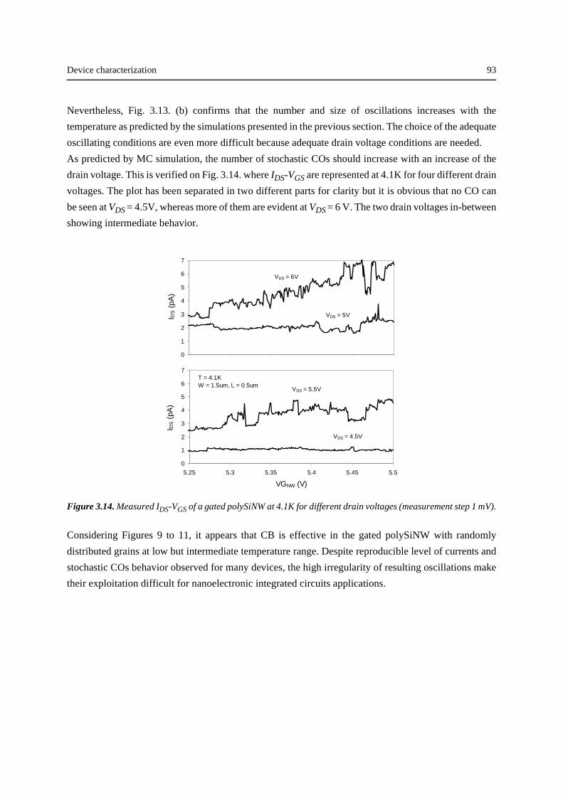
Device characterization 93
Nevertheless, Fig. 3.13. (b) confirms that the number and size of oscillations increases with the
temperature as predicted by the simulations presented in the previous section. The choice of the adequate
oscillating conditions are even more difficult because adequate drain voltage conditions are needed.
As predicted by MC simulation, the number of stochastic COs should increase with an increase of the
drain voltage. This is verified on Fig. 3.14. where IDS-VGS are represented at 4.1K for four different drain
voltages. The plot has been separated in two different parts for clarity but it is obvious that no CO can
be seen at VDS = 4.5V, whereas more of them are evident at VDS = 6 V. The two drain voltages in-between
showing intermediate behavior.
Figure 3.14. Measured IDS-VGS of a gated polySiNW at 4.1K for different drain voltages (measurement step 1 mV).
Considering Figures 9 to 11, it appears that CB is effective in the gated polySiNW with randomly
distributed grains at low but intermediate temperature range. Despite reproducible level of currents and
stochastic COs behavior observed for many devices, the high irregularity of resulting oscillations make
their exploitation difficult for nanoelectronic integrated circuits applications.
0
1
2
3
4
5
6
7
I DS (
pA)
VDS = 6V
VDS = 5V
0
1
2
3
4
5
6
7
5.25 5.3 5.35 5.4 5.45 5.5
VGNW (V)
I DS (
pA)
VDS = 5.5V
VDS = 4.5V
T = 4.1KW = 1.5um, L = 0.5um
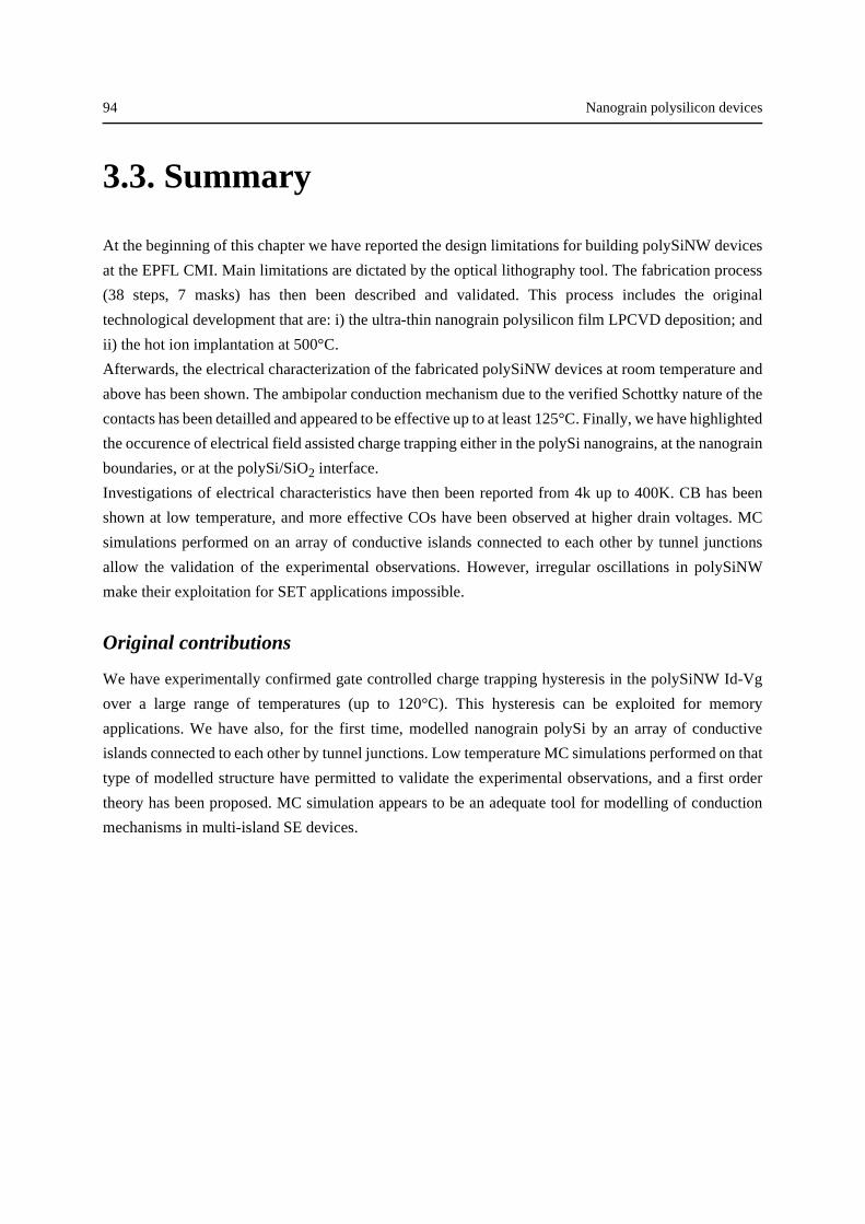
94 Nanograin polysilicon devices
3.3. Summary
At the beginning of this chapter we have reported the design limitations for building polySiNW devices
at the EPFL CMI. Main limitations are dictated by the optical lithography tool. The fabrication process
(38 steps, 7 masks) has then been described and validated. This process includes the original
technological development that are: i) the ultra-thin nanograin polysilicon film LPCVD deposition; and
ii) the hot ion implantation at 500°C.
Afterwards, the electrical characterization of the fabricated polySiNW devices at room temperature and
above has been shown. The ambipolar conduction mechanism due to the verified Schottky nature of the
contacts has been detailled and appeared to be effective up to at least 125°C. Finally, we have highlighted
the occurence of electrical field assisted charge trapping either in the polySi nanograins, at the nanograin
boundaries, or at the polySi/SiO2 interface.
Investigations of electrical characteristics have then been reported from 4k up to 400K. CB has been
shown at low temperature, and more effective COs have been observed at higher drain voltages. MC
simulations performed on an array of conductive islands connected to each other by tunnel junctions
allow the validation of the experimental observations. However, irregular oscillations in polySiNW
make their exploitation for SET applications impossible.
Original contributions
We have experimentally confirmed gate controlled charge trapping hysteresis in the polySiNW Id-Vg
over a large range of temperatures (up to 120°C). This hysteresis can be exploited for memory
applications. We have also, for the first time, modelled nanograin polySi by an array of conductive
islands connected to each other by tunnel junctions. Low temperature MC simulations performed on that
type of modelled structure have permitted to validate the experimental observations, and a first order
theory has been proposed. MC simulation appears to be an adequate tool for modelling of conduction
mechanisms in multi-island SE devices.
References 95
3.4. References
[1] VECTRON FD Swiss Sàrl, Puits-Godet 8, CH 2000 Neuchâtel.
[2] J. Appenzeller, J. Knoch, V. Derycke, R. Martel, S. Wind, and P. Avouris, "Field-Modulated CarrierTransport in Carbon Nanotube Transistors", Physical Review Letters, vol. 89 (12), pp. 126801, 2002.
[3] M. Pourfath, E. Ungersboeck, A. Gehring, B. H. Cheong, W. Park, H. Kosina, and S. Selberherr,"Improving the ambipolar Behaviro of Schottky Barrier Carbon Nanotube Field Effect Transistors",Proceedings of ESSDERC 2004, pp. 429-432, 2004.
[4] J. Guo, S. Datta, and M. Lundstrom, "A Numerical Study of Scaling Issues for Schottky-Barrier CarbonNanotube Transistors", IEEE Transactions on Electron Devices, vol. 51 (2), pp. 172-177, 2004.
[5] H.-C. Lin, K.-L. Yeh, T.-Y. Huang, R.-G. Huang, and S. M. Sze, "Ambipolar Schottky-Barrier TFTs", IEEETransactions on Electron Devices, vol. 49 (2), pp. 264-270, 2002.
[6] M. Nishisaka, S. Matsumoto, and T. Asano, "Schottky Source/Drain SOI Mosfet with Shallow DopedExtension", Japanese Journal of Applied Physics, vol. 42 (4B), pp. 2009-2013, 2003.
[7] M. M. Mandurah, K. C. Saraswat, and T. I. Kamins, "Phosphorous doping of Loe Pressure ChemicallyVapor-Deposited Silicon Films", Journal of the Electrochemical Society: Solid-State Science andTechnology, vol. 126 (6), pp. 1019-1023, 1979.
[8] C. Wasshuber, H. Kosina and S. Selberherr, "SIMON: a simulator for single-electron tunnel devices andcircuits", IEEE Transaction on Computer-Aided Design of Integrated Circuits and Systems, vol. 16 (9), pp.937-944, 1997.
[9] C. Wasshuber, "Computational Single-Electronics", Springer Verlag, Wien, 2001.
[10] I. M. Ruzin, V. Chandrasekhar, E. I. Levin, and L. I. Glazman, "Stochastic Coulomb blockade in a double-dot system", Physical Review B, vol. 45 (3), pp. 13469-13478, 1992.
[11] K. Kawamura, T. Kidera, A. Nakajima, and S. Yokoyama, "Coulomb blockade effects and conductionmechanism in extremely thin polycrystalline-silicon wires", Journal of Applied Physics, vol. 91 (8), pp.5213-5220, 2002.
[12] T. H. Wang, and S. Tarucha, "Effects of coupling and nonresonant tunneling on Coulomb blockadeoscillations in an asymmetric double dot structure", Applied Physics Letters, vol. 71 (17), pp. 2499-2501,1997.

96 Nanograin polysilicon devices
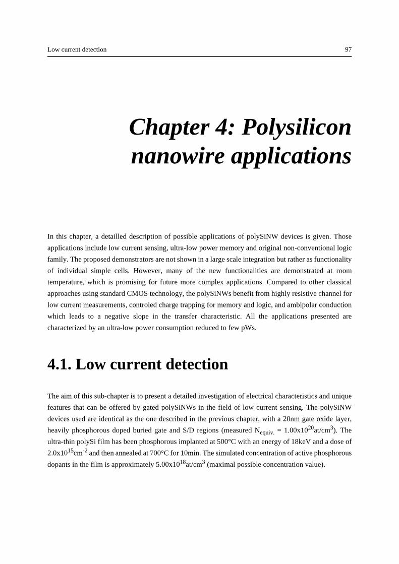
Low current detection 97
Chapter 4: Polysiliconnanowire applications
In this chapter, a detailled description of possible applications of polySiNW devices is given. Those
applications include low current sensing, ultra-low power memory and original non-conventional logic
family. The proposed demonstrators are not shown in a large scale integration but rather as functionality
of individual simple cells. However, many of the new functionalities are demonstrated at room
temperature, which is promising for future more complex applications. Compared to other classical
approaches using standard CMOS technology, the polySiNWs benefit from highly resistive channel for
low current measurements, controled charge trapping for memory and logic, and ambipolar conduction
which leads to a negative slope in the transfer characteristic. All the applications presented are
characterized by an ultra-low power consumption reduced to few pWs.
4.1. Low current detection
The aim of this sub-chapter is to present a detailed investigation of electrical characteristics and unique
features that can be offered by gated polySiNWs in the field of low current sensing. The polySiNW
devices used are identical as the one described in the previous chapter, with a 20nm gate oxide layer,
heavily phosphorous doped buried gate and S/D regions (measured Nequiv. = 1.00x10²⁰at/cm3). The
ultra-thin polySi film has been phosphorous implanted at 500°C with an energy of 18keV and a dose of
2.0x1015cm-2 and then annealed at 700°C for 10min. The simulated concentration of active phosphorous
dopants in the film is approximately 5.00x10¹⁸at/cm3 (maximal possible concentration value).

98 Polysilicon nanowire applications
4.1.1. Operation at constant current
As shown in the previous chapter (3.2.1.“Room temperature electrical characterization”) the gated
polySiNW devices have an ambipolar I-V characteristic as the one schematically illustrated on Fig. 4.1.
(b). Therefore, we suggest here an original bias scheme that exploits the distinct drain voltage current
dependence in the two conduction regimes. The operation consists of injecting a constant drain current
in the polySiNW (see Fig. 4.1. (a)) while the gate voltage is varied. The drain voltage, VDS, is first slowly
increasing versus VGS at constant drain current (holes conduction regime, see points 1,2,3 of Fig. 4.1. (b)
and (c)). The slight positive slope is then followed by an abrupt negative slope in the electron conduction,
which reflects a severe drop of VDS when VGS increases at constant current (see points 4 of Fig. 4.1. (b)
and (c)).
Figure 4.1. Schematics of: (a) the polySiNW and proposed bias scheme, with (b) the I-V typical characteristicsshowing V-shape, and (c) the resulting transfer characteristic at constant current.
Figure 4.2. Measured VDS-VGS transfer characteristics of polySiNW at four different constant currents.
Dra
in c
urr
ent,
I D(A
)
Gate voltage, VGS (V) Gate voltage, VGS (V)
Dra
in v
olt
age,
VD
S(V
)1 2 3 4
12
3
4
VDS
(b) (c)
(a)
2
3
4
5
6
7
8
9
1 1.5 2 2.5 3 3.5 4 4.5 5
Gate voltage, VGS (V)
Dra
in v
olta
ge, V
DS (
V)
IDS = 20pAstep = 5pA
IDS = 5pA
W = 0.3umL = 2um
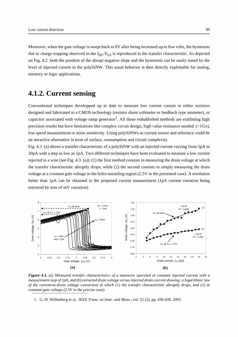
Low current detection 99
Moreover, when the gate voltage is swept back to 0V after being increased up to few volts, the hysteresis
due to charge trapping observed in the IDS-VGS is reproduced in the transfer characteristic. As depicted
on Fig. 4.2. both the position of the abrupt negative slope and the hysteresis can be easily tuned by the
level of injected current in the polySiNW. This usual behavior is then directly exploitable for analog,
memory or logic applications.
4.1.2. Current sensing
Conventional techniques developped up to date to measure low current consist in either resistors
designed and fabricated in a CMOS technology (resistor shunt voltmeter or feedback type ammeter), or
capacitor associated with voltage ramp generator1. All those esthablished methods are exhibiting high
precision results but have limitations like complex circuit design, high value resistance needed (>1Go),
low speed measurement or noise sensitivity. Using polySiNWs as current sensor and reference could be
an attractive alternative in term of surface, consumption and circuit complexity.
Fig. 4.3. (a) shows a transfer characteristic of a polySiNW with an injected current varying from 5pA to
20pA with a step as low as 1pA. Two different techniques have been evaluated to measure a low current
injected in a wire (see Fig. 4.3. (a)): (1) the first method consists in measuring the drain voltage at which
the transfer characteristic abruptly drops, while (2) the second consists in simply measuring the drain
voltage at a constant gate voltage in the holes tunneling region (2.5V in the presented case). A resolution
better than 1pA can be obtained in the proposed current measurement (1pA current variation being
mirrored by tens of mV variation).
Figure 4.3. (a) Measured transfer characteristics of a nanowire operated at constant injected current with ameasurement step of 1pA, and (b) extracted drain voltage versus injected drain current showing: a logarithmic lawof the current-to-drain voltage conversion at which (1) the transfer characteristic abruptly drops, and (2) atconstant gate voltage (2.5V in the precise case).
1. G.-D. Willenberg et al, IEEE Trans. on Instr. and Meas., vol. 52 (2), pp. 436-439, 2003.
2
3
4
5
6
7
8
2 2.25 2.5 2.75 3 3.25 3.5 3.75 4
Gate voltage, VGS (V)
Dra
in v
olta
ge, V
DS (
V)
IDS = 5pAstep = 1pA
IDS = 20pA
VDS @ peak W = 0.5um L = 2um
VDS @ VGS = 2.5V
(b)(a)
Log fit
R2 = 0.994
Log fit
R2 = 0.986
5.50
5.75
6.00
6.25
6.50
6.75
7.00
7.25
7.50
2 4 6 8 10 12 14 16 18 20 22
Drain current, IDS (pA)
Dra
in v
olta
ge, V
DS (
V)
(2)
(1)
VDS @ VGS = 2.5V
VDS @ peak
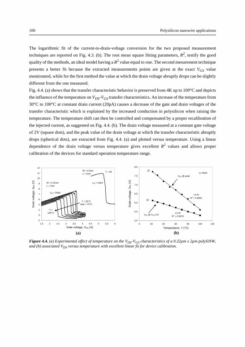
100 Polysilicon nanowire applications
The logarithmic fit of the current-to-drain-voltage conversion for the two proposed measurement
techniques are reported on Fig. 4.3. (b). The root mean square fitting parameters, R2, testify the good
quality of the methods, an ideal model having a R2 value equal to one. The second mesurement technique
presents a better fit because the extracted measurements points are given at the exact VGS value
mentionned, while for the first method the value at which the drain voltage abruptly drops can be slightly
different from the one measured.
Fig. 4.4. (a) shows that the transfer characteristic behavior is preserved from 4K up to 100°C and depicts
the influence of the temperature on VDS-VGS transfer characteristics. An increase of the temperature from
30°C to 100°C at constant drain current (20pA) causes a decrease of the gate and drain voltages of the
transfer characteristic which is explained by the increased conduction in polysilicon when raising the
temperature. The temperature shift can then be controlled and compensated by a proper recalibration of
the injected current, as suggested on Fig. 4.4. (b). The drain voltage measured at a constant gate voltage
of 2V (square dots), and the peak value of the drain voltage at which the transfer characteristic abruptly
drops (spherical dots), are extracted from Fig. 4.4. (a) and plotted versus temperature. Using a linear
dependence of the drain voltage versus temperature gives excellent R2 values and allows proper
calibration of the devices for standard operation temperature range.
Figure 4.4. (a) Experimental effect of temperature on the VDS-VGS characteristics of a 0.32µm x 2µm polySiNW,and (b) associated VDS versus temperature with excellent linear fit for device calibration.
Lin fit
R2 = 0.9979
Lin fit
R2 = 0.9961
5.0
5.5
6.0
6.5
7.0
7.5
8.0
0 20 40 60 80 100 120
Temperature, T (°C)
Dra
in v
olta
ge, V
DS (
V)
ID=20pAVDS @ peak
VDS @ VGS=2V
(1)
(2)
(b)(a)
2
3
4
5
6
7
8
9
10
11
12
1.5 2 2.5 3 3.5 4 4.5 5 5.5 6
Gate voltage, VGS (V)
Dra
in v
olta
ge, V
DS (
V)
T = 30°Cstep = 10°C
T = 100°C
IDS = 20pA
W = 0.32umL = 2um
W = 0.5umL = 2um
T = 4K
IDS = 10pA
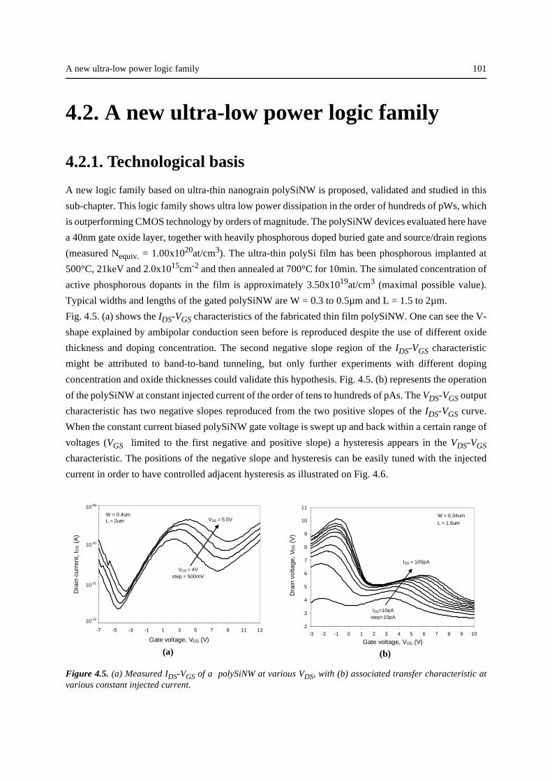
A new ultra-low power logic family 101
4.2. A new ultra-low power logic family
4.2.1. Technological basis
A new logic family based on ultra-thin nanograin polySiNW is proposed, validated and studied in this
sub-chapter. This logic family shows ultra low power dissipation in the order of hundreds of pWs, which
is outperforming CMOS technology by orders of magnitude. The polySiNW devices evaluated here have
a 40nm gate oxide layer, together with heavily phosphorous doped buried gate and source/drain regions
(measured Nequiv. = 1.00x10²⁰at/cm3). The ultra-thin polySi film has been phosphorous implanted at
500°C, 21keV and 2.0x1015cm-2 and then annealed at 700°C for 10min. The simulated concentration of
active phosphorous dopants in the film is approximately 3.50x10¹⁹at/cm3 (maximal possible value).
Typical widths and lengths of the gated polySiNW are W = 0.3 to 0.5µm and L = 1.5 to 2µm.
Fig. 4.5. (a) shows the IDS-VGS characteristics of the fabricated thin film polySiNW. One can see the V-
shape explained by ambipolar conduction seen before is reproduced despite the use of different oxide
thickness and doping concentration. The second negative slope region of the IDS-VGS characteristic
might be attributed to band-to-band tunneling, but only further experiments with different doping
concentration and oxide thicknesses could validate this hypothesis. Fig. 4.5. (b) represents the operation
of the polySiNW at constant injected current of the order of tens to hundreds of pAs. The VDS-VGS output
characteristic has two negative slopes reproduced from the two positive slopes of the IDS-VGS curve.
When the constant current biased polySiNW gate voltage is swept up and back within a certain range of
voltages (VGS limited to the first negative and positive slope) a hysteresis appears in the VDS-VGS
characteristic. The positions of the negative slope and hysteresis can be easily tuned with the injected
current in order to have controlled adjacent hysteresis as illustrated on Fig. 4.6.
Figure 4.5. (a) Measured IDS-VGS of a polySiNW at various VDS, with (b) associated transfer characteristic atvarious constant injected current.
-7 -5 -3 -1 1 3 5 7 9 11 13
Gate voltage, VGS (V)
Dra
in c
urre
nt, I
DS (
A)
VDS = 4Vstep = 500mV
VDS = 5.5V
10-12
10-11
10-10
10-09
W = 0.4umL = 2um
(a) (b)
2
3
4
5
6
7
8
9
10
11
-3 -2 -1 0 1 2 3 4 5 6 7 8 9 10
Gate voltage, VGS (V)
Dra
in v
olta
ge, V
DS (
V)
IDS=10pAstep=10pA
IDS = 100pA
W = 0.34um
L = 1.5um
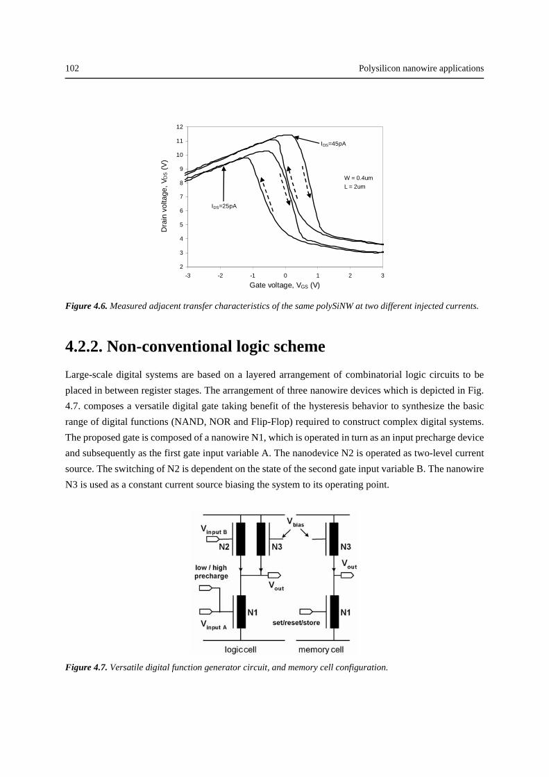
102 Polysilicon nanowire applications
Figure 4.6. Measured adjacent transfer characteristics of the same polySiNW at two different injected currents.
4.2.2. Non-conventional logic scheme
Large-scale digital systems are based on a layered arrangement of combinatorial logic circuits to be
placed in between register stages. The arrangement of three nanowire devices which is depicted in Fig.
4.7. composes a versatile digital gate taking benefit of the hysteresis behavior to synthesize the basic
range of digital functions (NAND, NOR and Flip-Flop) required to construct complex digital systems.
The proposed gate is composed of a nanowire N1, which is operated in turn as an input precharge device
and subsequently as the first gate input variable A. The nanodevice N2 is operated as two-level current
source. The switching of N2 is dependent on the state of the second gate input variable B. The nanowire
N3 is used as a constant current source biasing the system to its operating point.
Figure 4.7. Versatile digital function generator circuit, and memory cell configuration.
2
3
4
5
6
7
8
9
10
11
12
-3 -2 -1 0 1 2 3
Gate voltage, VGS (V)
Dra
in v
olta
ge, V
DS (
V)
IDS=25pA
IDS=45pA
W = 0.4um
L = 2um
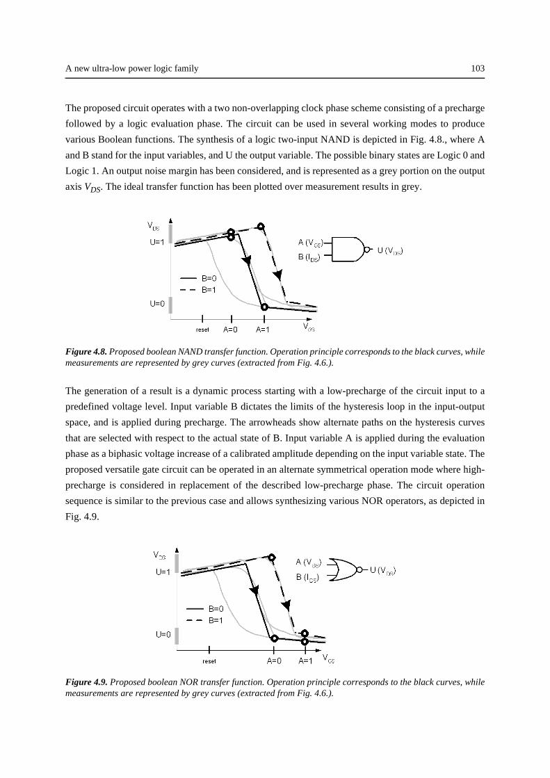
A new ultra-low power logic family 103
The proposed circuit operates with a two non-overlapping clock phase scheme consisting of a precharge
followed by a logic evaluation phase. The circuit can be used in several working modes to produce
various Boolean functions. The synthesis of a logic two-input NAND is depicted in Fig. 4.8., where A
and B stand for the input variables, and U the output variable. The possible binary states are Logic 0 and
Logic 1. An output noise margin has been considered, and is represented as a grey portion on the output
axis VDS. The ideal transfer function has been plotted over measurement results in grey.
Figure 4.8. Proposed boolean NAND transfer function. Operation principle corresponds to the black curves, whilemeasurements are represented by grey curves (extracted from Fig. 4.6.).
The generation of a result is a dynamic process starting with a low-precharge of the circuit input to a
predefined voltage level. Input variable B dictates the limits of the hysteresis loop in the input-output
space, and is applied during precharge. The arrowheads show alternate paths on the hysteresis curves
that are selected with respect to the actual state of B. Input variable A is applied during the evaluation
phase as a biphasic voltage increase of a calibrated amplitude depending on the input variable state. The
proposed versatile gate circuit can be operated in an alternate symmetrical operation mode where high-
precharge is considered in replacement of the described low-precharge phase. The circuit operation
sequence is similar to the previous case and allows synthesizing various NOR operators, as depicted in
Fig. 4.9.
Figure 4.9. Proposed boolean NOR transfer function. Operation principle corresponds to the black curves, whilemeasurements are represented by grey curves (extracted from Fig. 4.6.).
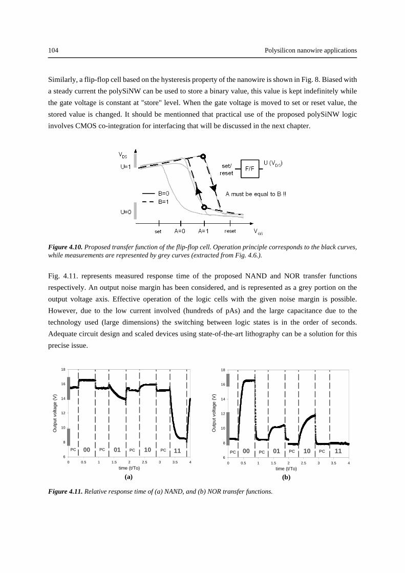
104 Polysilicon nanowire applications
Similarly, a flip-flop cell based on the hysteresis property of the nanowire is shown in Fig. 8. Biased with
a steady current the polySiNW can be used to store a binary value, this value is kept indefinitely while
the gate voltage is constant at "store" level. When the gate voltage is moved to set or reset value, the
stored value is changed. It should be mentionned that practical use of the proposed polySiNW logic
involves CMOS co-integration for interfacing that will be discussed in the next chapter.
Figure 4.10. Proposed transfer function of the flip-flop cell. Operation principle corresponds to the black curves,while measurements are represented by grey curves (extracted from Fig. 4.6.).
Fig. 4.11. represents measured response time of the proposed NAND and NOR transfer functions
respectively. An output noise margin has been considered, and is represented as a grey portion on the
output voltage axis. Effective operation of the logic cells with the given noise margin is possible.
However, due to the low current involved (hundreds of pAs) and the large capacitance due to the
technology used (large dimensions) the switching between logic states is in the order of seconds.
Adequate circuit design and scaled devices using state-of-the-art lithography can be a solution for this
precise issue.
Figure 4.11. Relative response time of (a) NAND, and (b) NOR transfer functions.
(b)(a)
6
8
10
12
14
16
18
0 0.5 1 1.5 2 2.5 3 3.5 4
time (t/To)
Out
put v
olta
ge (
V)
00 01 10 11PC PC PC PC6
8
10
12
14
16
18
0 0.5 1 1.5 2 2.5 3 3.5 4
time (t/To)
Out
put v
olta
ge (
V)
00 01 10 11PC PC PC PC
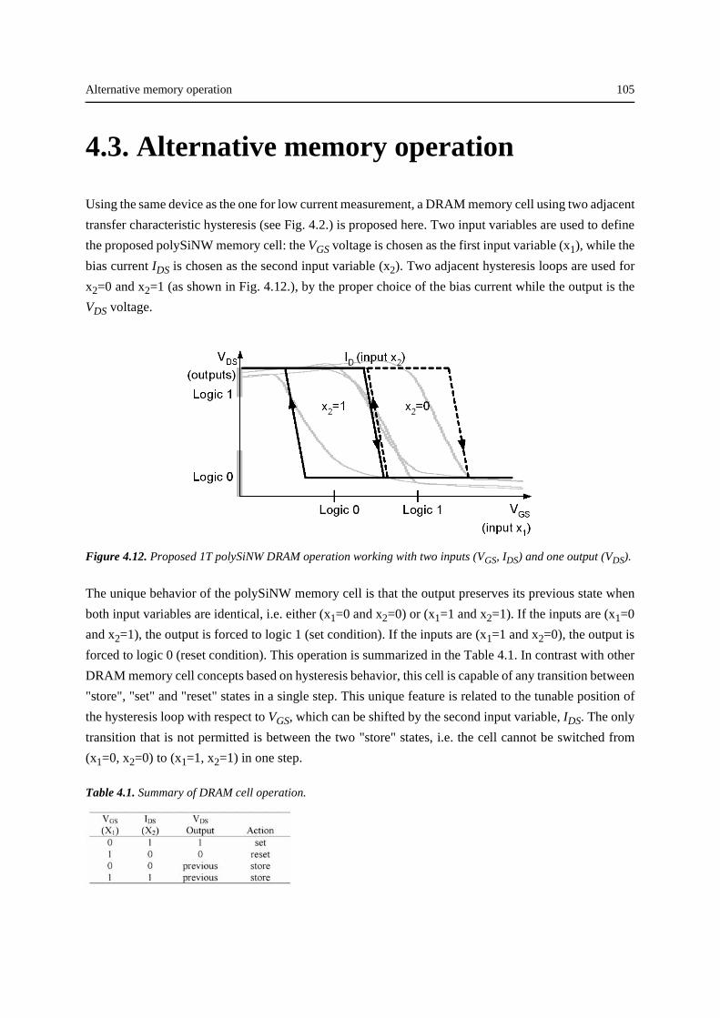
Alternative memory operation 105
4.3. Alternative memory operation
Using the same device as the one for low current measurement, a DRAM memory cell using two adjacent
transfer characteristic hysteresis (see Fig. 4.2.) is proposed here. Two input variables are used to define
the proposed polySiNW memory cell: the VGS voltage is chosen as the first input variable (x1), while the
bias current IDS is chosen as the second input variable (x2). Two adjacent hysteresis loops are used for
x2=0 and x2=1 (as shown in Fig. 4.12.), by the proper choice of the bias current while the output is the
VDS voltage.
Figure 4.12. Proposed 1T polySiNW DRAM operation working with two inputs (VGS, IDS) and one output (VDS).
The unique behavior of the polySiNW memory cell is that the output preserves its previous state when
both input variables are identical, i.e. either (x1=0 and x2=0) or (x1=1 and x2=1). If the inputs are (x1=0
and x2=1), the output is forced to logic 1 (set condition). If the inputs are (x1=1 and x2=0), the output is
forced to logic 0 (reset condition). This operation is summarized in the Table 4.1. In contrast with other
DRAM memory cell concepts based on hysteresis behavior, this cell is capable of any transition between
"store", "set" and "reset" states in a single step. This unique feature is related to the tunable position of
the hysteresis loop with respect to VGS, which can be shifted by the second input variable, IDS. The only
transition that is not permitted is between the two "store" states, i.e. the cell cannot be switched from
(x1=0, x2=0) to (x1=1, x2=1) in one step.
Table 4.1. Summary of DRAM cell operation.
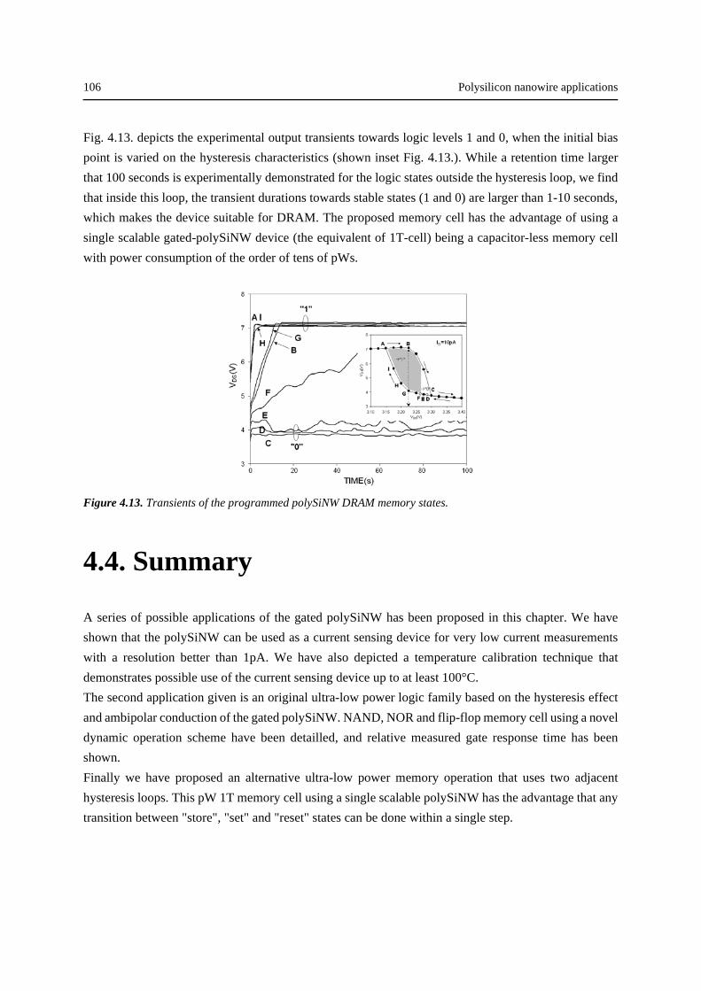
106 Polysilicon nanowire applications
Fig. 4.13. depicts the experimental output transients towards logic levels 1 and 0, when the initial bias
point is varied on the hysteresis characteristics (shown inset Fig. 4.13.). While a retention time larger
that 100 seconds is experimentally demonstrated for the logic states outside the hysteresis loop, we find
that inside this loop, the transient durations towards stable states (1 and 0) are larger than 1-10 seconds,
which makes the device suitable for DRAM. The proposed memory cell has the advantage of using a
single scalable gated-polySiNW device (the equivalent of 1T-cell) being a capacitor-less memory cell
with power consumption of the order of tens of pWs.
Figure 4.13. Transients of the programmed polySiNW DRAM memory states.
4.4. Summary
A series of possible applications of the gated polySiNW has been proposed in this chapter. We have
shown that the polySiNW can be used as a current sensing device for very low current measurements
with a resolution better than 1pA. We have also depicted a temperature calibration technique that
demonstrates possible use of the current sensing device up to at least 100°C.
The second application given is an original ultra-low power logic family based on the hysteresis effect
and ambipolar conduction of the gated polySiNW. NAND, NOR and flip-flop memory cell using a novel
dynamic operation scheme have been detailled, and relative measured gate response time has been
shown.
Finally we have proposed an alternative ultra-low power memory operation that uses two adjacent
hysteresis loops. This pW 1T memory cell using a single scalable polySiNW has the advantage that any
transition between "store", "set" and "reset" states can be done within a single step.
Summary 107
Original contributions
A new constant current bias scheme that exploits the V-shape (ambipolar) characteristics of the
fabricated polySiNW has been proposed and used for various applications. Major features of this bias
scheme are: (i) the very low constant current used to bias the polySiNW, (ii) the negative slope of the
transfer characteritics due to the ambipolar conduction of the gated polySiNW, and (iii) the controlled
hysteresis effect due to charge trapping in the polySi nanograins and/or at the polySi/SiO2 interface.
Combining all these properties, we have been able to suggest novel device operation for logic, memory
and current sensing together with ultra-low power consumption (few pWs). We think that this technique
is generally applicable for any other devices that present ambipolar (V-shape) characteristics, such as
CNTs or Schottky contact devices.

108 Polysilicon nanowire applications
Motivation 109
Chapter 5: CMOS-"nano"hybrid devices, circuits and
systems
5.1. Motivation
In the previous chapter, we have presented novel original features of polySiNW devices: (i) the high
resisitivity of the ultra-thin polySi channel serves for very low current sensing with a precision of few
pAs, (ii) the electrostatically controlled charge trapping in the polySiNW combined with (iii) the
ambipolar conduction due to the schottky nature of the contacts allows the building of ultra-low power
memory, and non-conventional logic family. In a more general manner, "after Moore" emerging
nanoelectronics like for example SETs, molecular electronics, CNTs, and/or spintronics have attracted
high interest because of their novel and unique properties. Their main advantages (see Table 5.1.) are the
nanoscale dimensions, the ultra-low power dissipation, and the novel functionalities (e.g. COs in SET
devices). Nevertheless, the price to pay for such properties is a very low current drive (slow devices),
low yield, poor reproducibility, and sometimes a lack of room temperature operation.
Table 5.1. summarizes the advantages and drawbacks of the emerging research devices versus ultimate
CMOS. Unlike "after Moore" research devices, CMOS benefits from high gain, high current drive, and
high speed, combined with good yield and very mature technology. On the counterpart, CMOS suffers
from scaling limitations, SCE, DIBL and increased power density. As a matter of fact, CMOS and
emerging nanoelectronics seems to be rather complementary. For example SET can bring new
functionality like COs and very low power consumption, while CMOS compensates SETs intrinsic
drawbacks with high-speed driving and voltage gain. Moreover, even if a stable and reliable "after
Moore" technology emerges in the near future replacement or competition with CMOS would be very
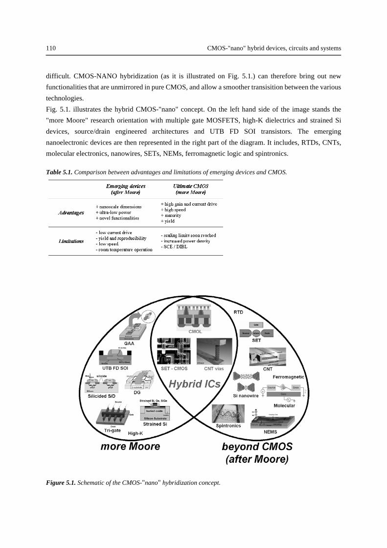
110 CMOS-"nano" hybrid devices, circuits and systems
difficult. CMOS-NANO hybridization (as it is illustrated on Fig. 5.1.) can therefore bring out new
functionalities that are unmirrored in pure CMOS, and allow a smoother transisition between the various
technologies.
Fig. 5.1. illustrates the hybrid CMOS-"nano" concept. On the left hand side of the image stands the
"more Moore" research orientation with multiple gate MOSFETS, high-K dielectrics and strained Si
devices, source/drain engineered architectures and UTB FD SOI transistors. The emerging
nanoelectronic devices are then represented in the right part of the diagram. It includes, RTDs, CNTs,
molecular electronics, nanowires, SETs, NEMs, ferromagnetic logic and spintronics.
Table 5.1. Comparison between advantages and limitations of emerging devices and CMOS.
Figure 5.1. Schematic of the CMOS-"nano" hybridization concept.
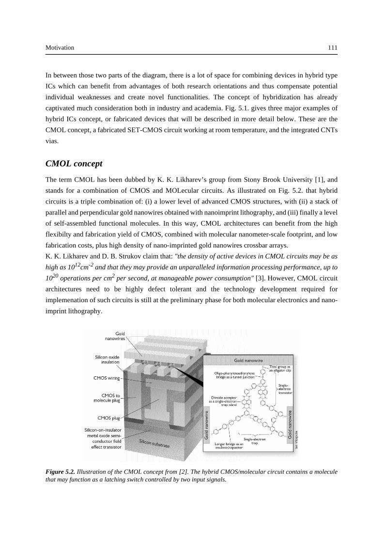
Motivation 111
In between those two parts of the diagram, there is a lot of space for combining devices in hybrid type
ICs which can benefit from advantages of both research orientations and thus compensate potential
individual weaknesses and create novel functionalities. The concept of hybridization has already
captivated much consideration both in industry and academia. Fig. 5.1. gives three major examples of
hybrid ICs concept, or fabricated devices that will be described in more detail below. These are the
CMOL concept, a fabricated SET-CMOS circuit working at room temperature, and the integrated CNTs
vias.
CMOL concept
The term CMOL has been dubbed by K. K. Likharev’s group from Stony Brook University [1], and
stands for a combination of CMOS and MOLecular circuits. As illustrated on Fig. 5.2. that hybrid
circuits is a triple combination of: (i) a lower level of advanced CMOS structures, with (ii) a stack of
parallel and perpendicular gold nanowires obtained with nanoimprint lithography, and (iii) finally a level
of self-assembled functional molecules. In this way, CMOL architectures can benefit from the high
flexibilty and fabrication yield of CMOS, combined with molecular nanometer-scale footprint, and low
fabrication costs, plus high density of nano-imprinted gold nanowires crossbar arrays.
K. K. Likharev and D. B. Strukov claim that: "the density of active devices in CMOL circuits may be as
high as 1012cm-2 and that they may provide an unparalleled information processing performance, up to
1020 operations per cm2 per second, at manageable power consumption" [3]. However, CMOL circuit
architectures need to be highly defect tolerant and the technology development required for
implemenation of such circuits is still at the preliminary phase for both molecular electronics and nano-
imprint lithography.
Figure 5.2. Illustration of the CMOL concept from [2]. The hybrid CMOS/molecular circuit contains a moleculethat may function as a latching switch controlled by two input signals.
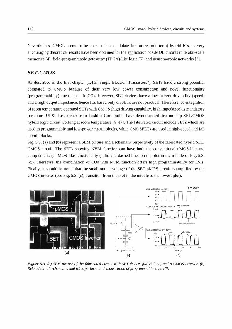
112 CMOS-"nano" hybrid devices, circuits and systems
Nevertheless, CMOL seems to be an excellent candidate for future (mid-term) hybrid ICs, as very
encouraging theoretical results have been obtained for the application of CMOL circuits in terabit-scale
memories [4], field-programmable gate array (FPGA)-like logic [5], and neuromorphic networks [3].
SET-CMOS
As described in the first chapter (1.4.3.“Single Electron Transistors”), SETs have a strong potential
compared to CMOS because of their very low power consumption and novel functionality
(programmability) due to specific COs. However, SET devices have a low current drivability (speed)
and a high output impedance, hence ICs based only on SETs are not practical. Therefore, co-integration
of room temperature operated SETs with CMOS (high driving capability, high impedance) is mandatory
for future ULSI. Researcher from Toshiba Corporation have demonstrated first on-chip SET/CMOS
hybrid logic circuit working at room temperature [6]-[7]. The fabricated circuit include SETs which are
used in programmable and low-power circuit blocks, while CMOSFETs are used in high-speed and I/O
circuit blocks.
Fig. 5.3. (a) and (b) represent a SEM picture and a schematic respectively of the fabricated hybrid SET/
CMOS circuit. The SETs showing NVM function can have both the conventional nMOS-like and
complementary pMOS-like functionality (solid and dashed lines on the plot in the middle of Fig. 5.3.
(c)). Therefore, the combination of COs with NVM function offers high programmability for LSIs.
Finally, it should be noted that the small output voltage of the SET-pMOS circuit is amplified by the
CMOS inverter (see Fig. 5.3. (c), transition from the plot in the middle to the lowest plot).
Figure 5.3. (a) SEM picture of the fabricated circuit with SET device, pMOS load, and a CMOS inverter. (b)Related circuit schematic, and (c) experimental demonstration of programmable logic [6].
(c)(a)
(b)
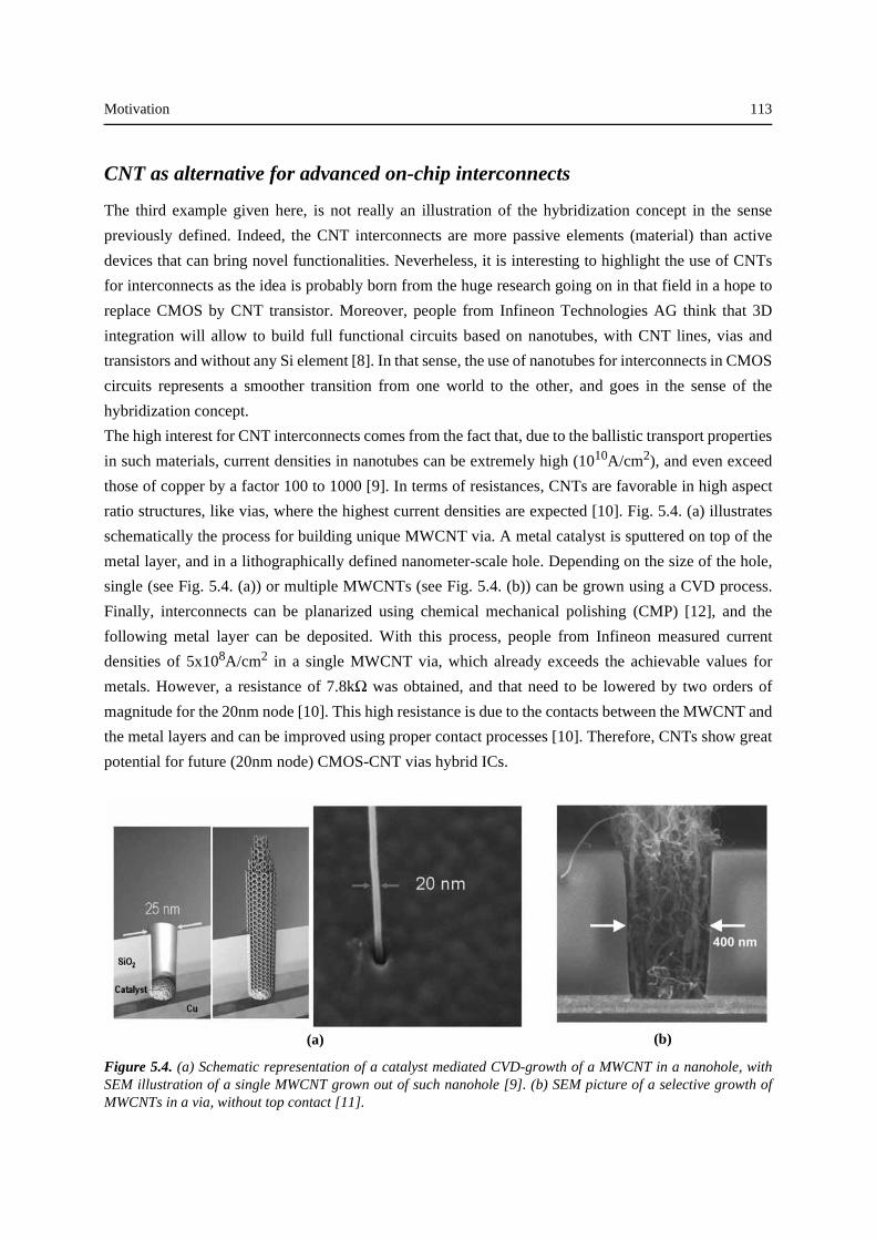
Motivation 113
CNT as alternative for advanced on-chip interconnects
The third example given here, is not really an illustration of the hybridization concept in the sense
previously defined. Indeed, the CNT interconnects are more passive elements (material) than active
devices that can bring novel functionalities. Neverheless, it is interesting to highlight the use of CNTs
for interconnects as the idea is probably born from the huge research going on in that field in a hope to
replace CMOS by CNT transistor. Moreover, people from Infineon Technologies AG think that 3D
integration will allow to build full functional circuits based on nanotubes, with CNT lines, vias and
transistors and without any Si element [8]. In that sense, the use of nanotubes for interconnects in CMOS
circuits represents a smoother transition from one world to the other, and goes in the sense of the
hybridization concept.
The high interest for CNT interconnects comes from the fact that, due to the ballistic transport properties
in such materials, current densities in nanotubes can be extremely high (1010A/cm2), and even exceed
those of copper by a factor 100 to 1000 [9]. In terms of resistances, CNTs are favorable in high aspect
ratio structures, like vias, where the highest current densities are expected [10]. Fig. 5.4. (a) illustrates
schematically the process for building unique MWCNT via. A metal catalyst is sputtered on top of the
metal layer, and in a lithographically defined nanometer-scale hole. Depending on the size of the hole,
single (see Fig. 5.4. (a)) or multiple MWCNTs (see Fig. 5.4. (b)) can be grown using a CVD process.
Finally, interconnects can be planarized using chemical mechanical polishing (CMP) [12], and the
following metal layer can be deposited. With this process, people from Infineon measured current
densities of 5x10⁸A/cm2 in a single MWCNT via, which already exceeds the achievable values for
metals. However, a resistance of 7.8kΩ was obtained, and that need to be lowered by two orders of
magnitude for the 20nm node [10]. This high resistance is due to the contacts between the MWCNT and
the metal layers and can be improved using proper contact processes [10]. Therefore, CNTs show great
potential for future (20nm node) CMOS-CNT vias hybrid ICs.
Figure 5.4. (a) Schematic representation of a catalyst mediated CVD-growth of a MWCNT in a nanohole, withSEM illustration of a single MWCNT grown out of such nanohole [9]. (b) SEM picture of a selective growth ofMWCNTs in a via, without top contact [11].
(a) (b)
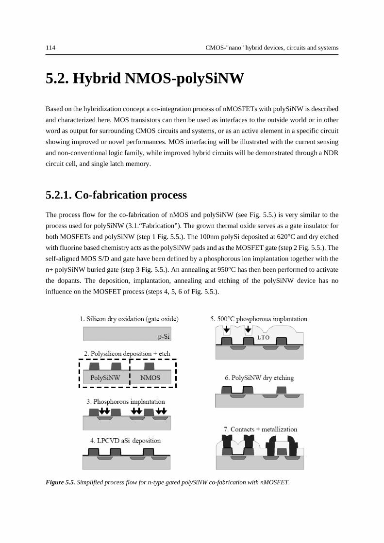
114 CMOS-"nano" hybrid devices, circuits and systems
5.2. Hybrid NMOS-polySiNW
Based on the hybridization concept a co-integration process of nMOSFETs with polySiNW is described
and characterized here. MOS transistors can then be used as interfaces to the outside world or in other
word as output for surrounding CMOS circuits and systems, or as an active element in a specific circuit
showing improved or novel performances. MOS interfacing will be illustrated with the current sensing
and non-conventional logic family, while improved hybrid circuits will be demonstrated through a NDR
circuit cell, and single latch memory.
5.2.1. Co-fabrication process
The process flow for the co-fabrication of nMOS and polySiNW (see Fig. 5.5.) is very similar to the
process used for polySiNW (3.1.“Fabrication”). The grown thermal oxide serves as a gate insulator for
both MOSFETs and polySiNW (step 1 Fig. 5.5.). The 100nm polySi deposited at 620°C and dry etched
with fluorine based chemistry acts as the polySiNW pads and as the MOSFET gate (step 2 Fig. 5.5.). The
self-aligned MOS S/D and gate have been defined by a phosphorous ion implantation together with the
n+ polySiNW buried gate (step 3 Fig. 5.5.). An annealing at 950°C has then been performed to activate
the dopants. The deposition, implantation, annealing and etching of the polySiNW device has no
influence on the MOSFET process (steps 4, 5, 6 of Fig. 5.5.).
Figure 5.5. Simplified process flow for n-type gated polySiNW co-fabrication with nMOSFET.
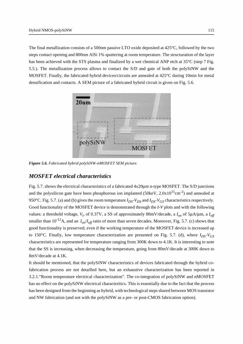
Hybrid NMOS-polySiNW 115
The final metallization consists of a 500nm passive LTO oxide deposited at 425°C, followed by the two
steps contact opening and 800nm AlSi 1% sputtering at room temperature. The structuration of the layer
has been achieved with the STS plasma and finalized by a wet chemical ANP etch at 35°C (step 7 Fig.
5.5.). The metallization process allows to contact the S/D and gate of both the polySiNW and the
MOSFET. Finally, the fabricated hybrid devices/circuits are annealed at 425°C during 10min for metal
densification and contacts. A SEM picture of a fabricated hybrid circuit is given on Fig. 5.6.
Figure 5.6. Fabricated hybrid polySiNW-nMOSFET SEM picture.
MOSFET electrical characteristics
Fig. 5.7. shows the electrical characteristics of a fabricated 4x20µm n-type MOSFET. The S/D junctions
and the polysilicon gate have been phosphorous ion implanted (50keV, 2.0x1015cm-2) and annealed at
950°C. Fig. 5.7. (a) and (b) gives the room temperature IDS-VDS and IDS-VGS characteristics respectively.
Good functionality of the MOSFET device is demonstrated through the I-V plots and with the following
values: a threshold voltage, Vt, of 0.37V, a SS of approximately 80mV/decade, a Ion of 5µA/µm, a Ioff
smaller than 10-12A, and an Ion/Ioff ratio of more than seven decades. Moreover, Fig. 5.7. (c) shows that
good functionality is preserved, even if the working temperature of the MOSFET device is increased up
to 150°C. Finally, low temperature characterization are presented on Fig. 5.7. (d), where IDS-VGS
characteristics are represented for temperature ranging from 300K down to 4.1K. It is interesting to note
that the SS is increasing, when decreasing the temperature, going from 80mV/decade at 300K down to
8mV/decade at 4.1K.
It should be mentioned, that the polySiNW characteristics of devices fabricated through the hybrid co-
fabrication process are not detailled here, but an exhaustive characterization has been reported in
3.2.1.“Room temperature electrical characterization”. The co-integration of polySiNW and nMOSFET
has no effect on the polySiNW electrical characteritics. This is essentially due to the fact that the process
has been designed from the beginning as hybrid, with technological steps shared between MOS transistor
and NW fabrication (and not with the polySiNW as a pre- or post-CMOS fabrication option).
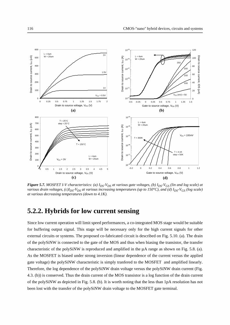
116 CMOS-"nano" hybrid devices, circuits and systems
Figure 5.7. MOSFET I-V characteristics: (a) IDS-VDS at various gate voltages, (b) IDS-VGS (lin and log scale) atvarious drain voltages, (c)IDS-VDS at various increasing temperatures (up to 150°C), and (d) IDS-VGS (log scale)at various decreasing temperatures (down to 4.1K).
5.2.2. Hybrids for low current sensing
Since low current operation will limit speed performances, a co-integrated MOS stage would be suitable
for buffering output signal. This stage will be necessary only for the high current signals for other
external circuits or systems. The proposed co-fabricated circuit is described on Fig. 5.10. (a). The drain
of the polySiNW is connected to the gate of the MOS and thus when biasing the transistor, the transfer
characteristic of the polySiNW is reproduced and amplified in the µA range as shown on Fig. 5.8. (a).
As the MOSFET is biased under strong inversion (linear dependence of the current versus the applied
gate voltage) the polySiNW characteristic is simply tranfered to the MOSFET and amplified linearly.
Therefore, the log dependence of the polySiNW drain voltage versus the polySiNW drain current (Fig.
4.3. (b)) is conserved. Thus the drain current of the MOS transistor is a log function of the drain current
of the polySiNW as depicted in Fig. 5.8. (b). It is worth noting that the less than 1pA resolution has not
been lost with the transfer of the polySiNW drain voltage to the MOSFET gate terminal.
0
100
200
300
400
500
600
0 0.25 0.5 0.75 1 1.25 1.5 1.75 2
Drain to source voltage, VDS (V)
Dra
in to
sou
rce
curr
ent,
I DS (µ
A)
L = 4umW = 20um
VGS = 0.5V
1V
1.5V
2V
-0.5 -0.25 0 0.25 0.5 0.75 1 1.25 1.5
Gate to source voltage, VGS (V)
Dra
in to
sou
rce
curr
ent,
I DS (
A)
0
20
40
60
80
100
120
Drain to source current, ID
S ( µ
A)
10-13
10-11
10-09
10-07
10-05
10-03
VDS (mV) = 50
100
150
200
250
L = 4umW = 20um
(a) (b)
-0.2 0 0.2 0.4 0.6 0.8 1 1.2
Gate to source voltage, VGS (V)
Dra
in to
sou
rce
curr
ent,
I DS (
A)
10-13
10-11
10-09
10-07
10-05
10-03
L = 4umW = 20um
VDS = 100mV
T = 4.1Kstep = 50K
T = 300K
0
100
200
300
400
500
600
700
800
0 0.5 1 1.5 2 2.5 3 3.5 4 4.5 5
Drain to source voltage, VDS (V)
Dra
in to
sou
rce
curr
ent,
I DS (µ
A)
L = 4umW = 20umVGS = 3V
T = 25°Cstep = 25°C
T = 150°C
(c) (d)
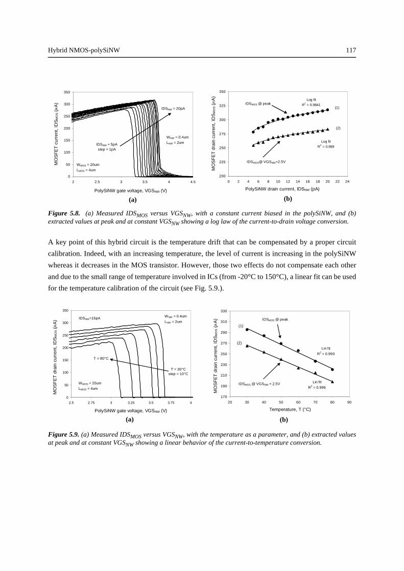
Hybrid NMOS-polySiNW 117
Figure 5.8. (a) Measured IDSMOS versus VGSNW, with a constant current biased in the polySiNW, and (b)extracted values at peak and at constant VGSNW showing a log law of the current-to-drain voltage conversion.
A key point of this hybrid circuit is the temperature drift that can be compensated by a proper circuit
calibration. Indeed, with an increasing temperature, the level of current is increasing in the polySiNW
whereas it decreases in the MOS transistor. However, those two effects do not compensate each other
and due to the small range of temperature involved in ICs (from -20°C to 150°C), a linear fit can be used
for the temperature calibration of the circuit (see Fig. 5.9.).
Figure 5.9. (a) Measured IDSMOS versus VGSNW, with the temperature as a parameter, and (b) extracted valuesat peak and at constant VGSNW showing a linear behavior of the current-to-temperature conversion.
0
50
100
150
200
250
300
350
2 2.5 3 3.5 4 4.5
PolySiNW gate voltage, VGSNW (V)
MO
SF
ET
cur
rent
, ID
SM
OS (µ
A)
IDSNW = 5pAstep = 1pA
IDSNW = 20pA
WNW = 0.4um
LNW = 2um
WMOS = 20um
LMOS = 4um
(a) (b)
Log fit
R2 = 0.989
Log fit
R2 = 0.9841
200
225
250
275
300
325
350
0 2 4 6 8 10 12 14 16 18 20 22 24
PolySiNW drain current, IDSNW (pA)
MO
SF
ET
dra
in c
urre
nt, I
DS
MO
S (µ
A)
IDSMOS @ peak
IDSMOS@ VGSNW=2.5V
(1)
(2)
(a) (b)
0
50
100
150
200
250
300
350
2.5 2.75 3 3.25 3.5 3.75 4
PolySiNW gate voltage, VGSNW (V)
MO
SF
ET
dra
in c
urre
nt, I
DS
MO
S (µ
A)
T = 80°C
T = 30°Cstep = 10°C
IDSNW=15pA
WMOS = 20um
LMOS = 4um
WNW = 0.4um
LNW = 2um
Lin fit
R2 = 0.996
Lin fit
R2 = 0.993
170
190
210
230
250
270
290
310
330
20 30 40 50 60 70 80 90
Temperature, T (°C)
MO
SF
ET
dra
in c
urre
nt, I
DS
MO
S (µ
A) IDSMOS @ peak
IDSMOS @ VGSNW = 2.5V
(1)
(2)
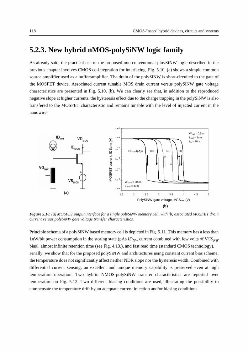
118 CMOS-"nano" hybrid devices, circuits and systems
5.2.3. New hybrid nMOS-polySiNW logic family
As already said, the practical use of the proposed non-conventional ploySiNW logic described in the
previous chapter involves CMOS co-integration for interfacing. Fig. 5.10. (a) shows a simple common
source amplifier used as a buffer/amplifier. The drain of the polySiNW is short-circuited to the gate of
the MOSFET device. Associated current tunable MOS drain current versus polySiNW gate voltage
characteristics are presented in Fig. 5.10. (b). We can clearly see that, in addition to the reproduced
negative slope at higher currents, the hysteresis effect due to the charge trapping in the polySiNW is also
transfered to the MOSFET characteristic and remains tunable with the level of injected current in the
nanowire.
Figure 5.10. (a) MOSFET output interface for a single polySiNW memory cell, with (b) associated MOSFET draincurrent versus polySiNW gate voltage transfer characteristics.
Principle schema of a polySiNW based memory cell is depicted in Fig. 5.11. This memory has a less than
1nW/bit power consumption in the storing state (pAs IDNW current combined with few volts of VGSNW
bias), almost infinite retention time (see Fig. 4.13.), and fast read time (standard CMOS technology).
Finally, we show that for the proposed polySiNW and architectures using constant current bias scheme,
the temperature does not significantly affect neither NDR slope nor the hysteresis width. Combined with
differential current sensing, an excellent and unique memory capability is preserved even at high
temperature operation. Two hybrid NMOS-polySiNW transfer characteristics are reported over
temperature on Fig. 5.12. Two different biasing conditions are used, illustrating the possibility to
compensate the temperature drift by an adequate current injection and/or biasing conditions.
1.5 2 2.5 3 3.5 4 4.5 5
PolySiNW gate voltage, VGSNW (V)
MO
SF
ET
cur
rent
, ID
SM
OS (
A)
IDSNW (pA)= 140100 180
WNW = 0.5um
LNW = 2um
tox = 40nm
10-9
10-8
10-7
10-6
10-5
10-4
10-3
WMOS = 20um
LMOS = 4um
(b)
(a)
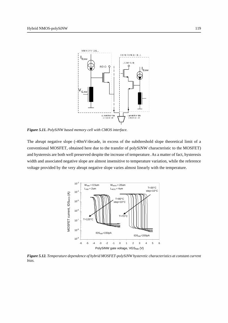
Hybrid NMOS-polySiNW 119
Figure 5.11. PolySiNW based memory cell with CMOS interface.
The abrupt negative slope (-40mV/decade, in excess of the subthreshold slope theoretical limit of a
conventional MOSFET, obtained here due to the transfer of polySiNW characteristic to the MOSFET)
and hysteresis are both well preserved despite the increase of temperature. As a matter of fact, hysteresis
width and associated negative slope are almost insensitive to temperature variation, while the reference
voltage provided by the very abrupt negative slope varies almost linearly with the temperature.
Figure 5.12. Temperature dependence of hybrid MOSFET-polySiNW hysteretic characteristics at constant currentbias.
-6 -5 -4 -3 -2 -1 0 1 2 3 4 5 6
PolySiNW gate voltage, VGSNW (V)
MO
SF
ET
cur
rent
, ID
SM
OS (
A)
IDSNW=150pAIDSNW=200pA
T=80°Cstep=10°C
T=120°C
T=30°Cstep=10°C
T=70°C
WNW = 0.5um
LNW = 2um
WMOS = 20um
LMOS = 4um
10-9
10-8
10-7
10-6
10-5
10-4
10-3
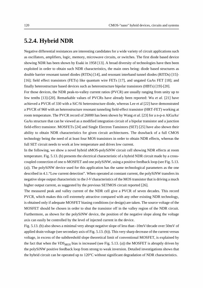
120 CMOS-"nano" hybrid devices, circuits and systems
5.2.4. Hybrid NDR
Negative differential resistances are interesting candidates for a wide variety of circuit applications such
as oscillators, amplifiers, logic, memory, microwave circuits, or switches. The first diode based device
showing NDR has been shown by Esaki in 1958 [13]. A broad diversity of technologies have then been
exploited in order to obtain such NDR characteristics, the main ones being: diode based structures as
double barrier resonant tunnel diodes (RTDs) [14], and resonant interband tunnel diodes (RITDs) [15]-
[16]; field effect transistors (FETs) like quantum wire FETs [17], and ungated GaAs FET [18]; and
finally heterostructure based devices such as heterostructure bipolar transistors (HBTs) [19]-[20].
For those devices, the NDR peak-to-valley current ratios (PVCR) are usually ranging from unity up to
few tenths [13]-[20]. Remarkable values of PVCRs have already been reported: Wu et al. [21] have
achieved a PVCR of 330 with a SiC/Si heterostructure diode, whereas Lee et al [22] have demonstrated
a PVCR of 960 with an heterostructure resonant tunneling field-effect transistor (HRT-FET) working at
room temperature. The PVCR record of 26000 has been shown by Wang et al. [23] for a n-p-n AlGaAs/
GaAs structure that can be viewed as a modified integration circuit of a bipolar transistor and a junction
field-effect transistor. MOSFETs [24] and Single Electron Tansistors (SET) [25] have also shown their
ability to obtain NDR characteristics for given circuit architectures. The drawback of a full CMOS
technology being the need of at least four MOS transistors in order to obtain NDR effects, whereas the
full SET circuit needs to work at low temperature and drives low current.
In the following, we show a novel hybrid nMOS-polySiNW circuit cell showing NDR effects at room
temperature. Fig. 5.13. (b) presents the electrical characteristic of a hybrid NDR circuit made by a cross-
coupled connection of one n-MOSFET and one polySiNW, using a positive feedback loop (see Fig. 5.13.
(a)). The polySiNW device used for this application has the same technological parameters as the one
described in 4.1.“Low current detection”. When operated at constant current, the polySiNW transfers its
negative slope output characteristic to the I-V characteristics of the MOS transistor that is driving a much
higher output current, as suggested by the previous SETMOS circuit reported [26].
The measured peak and valley current of the NDR cell give a PVCR of seven decades. This record
PVCR, which makes this cell extremely attractive compared with any other existing NDR technology,
is obtained only if adequate MOSFET biasing conditions (or design) are taken. The source voltage of the
MOSFET should be chosen in order to shut the transistor off in the valley region of the NDR circuit.
Furthermore, as shown for the polySiNW device, the position of the negative slope along the voltage
axis can easily be controlled by the level of injected current in the device.
Fig. 5.13. (b) also shows a minimal very abrupt negative slope of less than -10mV/decade over 50mV of
applied drain voltage (see secondary axis of Fig. 5.13. (b)). This very sharp decrease of the current versus
voltage, in excess of the subthreshold slope theoretical limit of conventional MOSFET, is explained by
the fact that when the VDSMOS bias is increased (see Fig. 5.13. (a)) the MOSFET is abruptly driven by
the polySiNW positive feedback loop from strong to weak inversion. Detailed investigations shows that
the hybrid circuit can be operated up to 120°C without significant degradation of NDR characteristics.
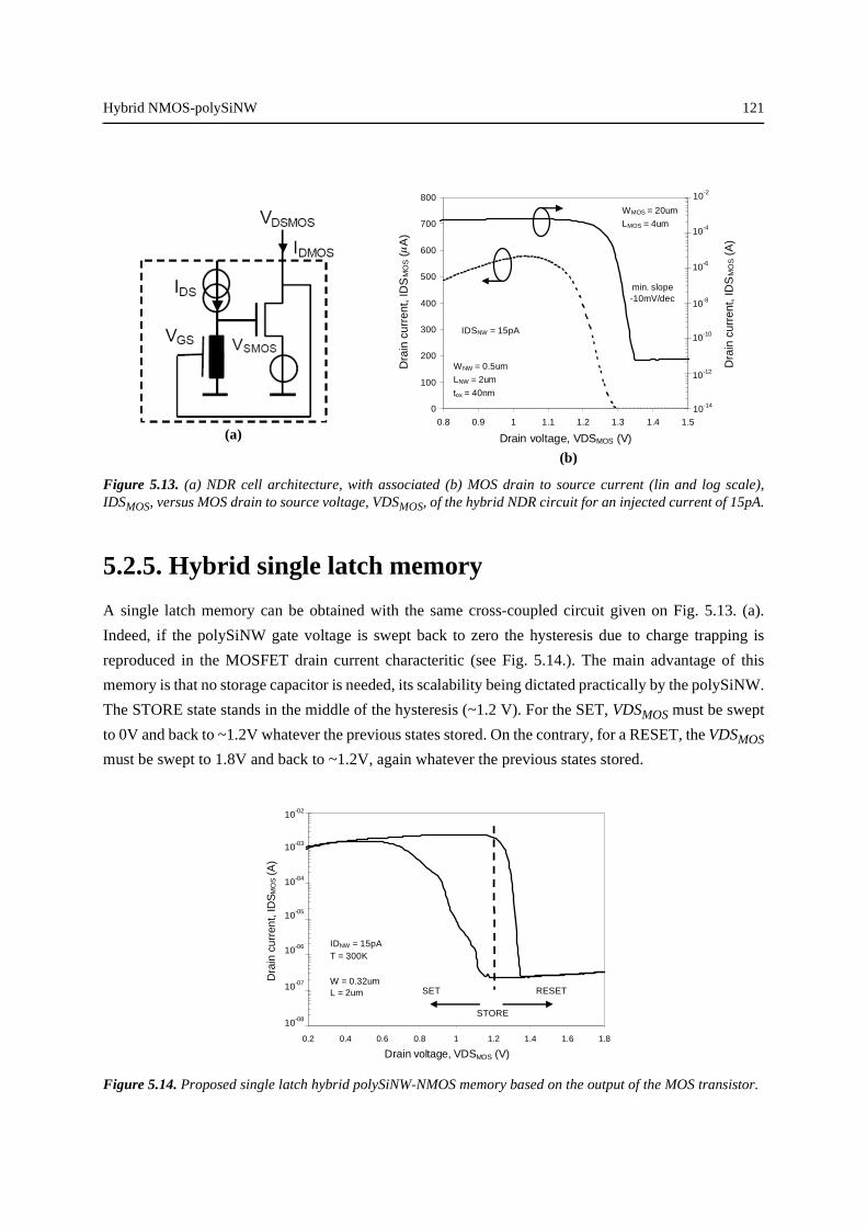
Hybrid NMOS-polySiNW 121
Figure 5.13. (a) NDR cell architecture, with associated (b) MOS drain to source current (lin and log scale),IDSMOS, versus MOS drain to source voltage, VDSMOS, of the hybrid NDR circuit for an injected current of 15pA.
5.2.5. Hybrid single latch memory
A single latch memory can be obtained with the same cross-coupled circuit given on Fig. 5.13. (a).
Indeed, if the polySiNW gate voltage is swept back to zero the hysteresis due to charge trapping is
reproduced in the MOSFET drain current characteritic (see Fig. 5.14.). The main advantage of this
memory is that no storage capacitor is needed, its scalability being dictated practically by the polySiNW.
The STORE state stands in the middle of the hysteresis (~1.2 V). For the SET, VDSMOS must be swept
to 0V and back to ~1.2V whatever the previous states stored. On the contrary, for a RESET, the VDSMOS
must be swept to 1.8V and back to ~1.2V, again whatever the previous states stored.
Figure 5.14. Proposed single latch hybrid polySiNW-NMOS memory based on the output of the MOS transistor.
0
100
200
300
400
500
600
700
800
0.8 0.9 1 1.1 1.2 1.3 1.4 1.5
Drain voltage, VDSMOS (V)
Dra
in c
urre
nt, I
DS
MO
S (µ
A)
Dra
in c
urre
nt, I
DS
MO
S (
A)
10-14
10-12
10-10
10-8
10-6
10-4
10-2
min. slope-10mV/dec
WMOS = 20um
LMOS = 4um
WNW = 0.5um
LNW = 2um
tox = 40nm
IDSNW = 15pA
(b)
(a)
0.2 0.4 0.6 0.8 1 1.2 1.4 1.6 1.8
Drain voltage, VDSMOS (V)
Dra
in c
urre
nt, I
DS
MO
S (
A)
IDNW = 15pAT = 300K
W = 0.32umL = 2um
STORE
SET RESET
10-02
10-08
10-07
10-06
10-05
10-04
10-03
122 CMOS-"nano" hybrid devices, circuits and systems
5.3. Summary
In this chapter we have first described a hybrid CMOS-"nano" concept. Hybridization of advanced
CMOS devices ("more Moore") together with emerging nanoelectronics structures (beyond CMOS, or
"after Moore") allows to bring out novel functionalities and higher performances that are unmirrored in
pure CMOS technology. Moreover, hybrid integration permits a smoother transition between the "end
of CMOS", and the "beyond CMOS" era.
The hybrid CMOS-"nano" concept has then been illustrated with: (i) the CMOL architecture that shows
density of active devices as high as 1012cm-2 together with unparalleled processing performances, up to
1020 operations per cm2 per second, at manageable power consumption; (ii) the first on-chip SET/CMOS
hybrid logic circuit working at room temperature, which opens a way to ultra-low power LSIs; and (iii)
the use of CNT interconnects in CMOS ICs, for higher achievable current densities in vias from the
20nm node and beyond.
Subsequently, we have applied a similar hybridization scheme to our polySiNW devices. Indeed, co-
fabrication of nMOSFET transistors with gated polySiNWs has been presented, and the good MOSFET
electrical characteristics from low temperature (4.1K) up to 150°C have been demonstrated. Afterwards,
the practical use of fabricated hybrid nMOSFET-polySiNW circuits has been illustrated with four
different applications: (i) low current sensing hybrid circuits using co-integrated MOS stage for
buffering the output signal at higher current; (ii) a new low power hybrid nMOS-polySiNW logic family
where nMOSFETs are used as interfaces; (iii) a hybrid NDR circuit cell showing record performances
in terms of PVCR and negative SS; and (iv) a hybrid nMOS-polySiNW single latch memory. The
functionality of the hybrid circuits has been demonstrated from room temperature up to at least 120°C.
Original contributions
The hybridization of polySiNW devices (ambipolar conduction and hysteresis effect) together with high
current drive nMOSFETs, have permitted the design of original circuit cells having novel functionalities
and/or outperforming characteristics. Indeed, the new logic family proposed in this chapter combines an
original working principle jointly with low power consumption. The fabricated hybrid NDR circuit cell
shows a record PVCR of more than seven decades, with a negative subthreshold slope of less than
-10mV/decade. Finally, the low current sensing hybrid circuit allows to measure very low current with
a precision of at least 1pA and an output of hundreds of µAs.
References 123
5.4. References
[1] Available online at http://pavel.physics.sunysb.edu/~likharev/personal/.
[2] K. K. Likharev, "Hybrid Semiconductor-Molecular Nanoelectronics", The Industrial Physicist, vol. 9 (3),pp. 20-23, 2003.
[3] K. K. Likharev, and D. B. Strukov, "CMOL: Devices, Circuits, and Architectures", in G. Cuniberti et al.(eds.), Introducing Molecular Electronics, pp. 447-477, Springer, 2005.
[4] D. B. Strukov, and K. K. Likharev, "Prospects for terabit-scale nanoelectronic memories", Nanotechnology,vol. 16 (1), pp. 137-148, 2005.
[5] D. B. Strukov, and K. K. Likharev, "CMOL FPGA: a reconfigurable architecture for hybrid digital circuitswith two-terminal nanodevices", Nanotechnology, vol. 16 (6), pp. 888-900 , 2005.
[6] K. Uchida, J. Koga, R. Ohba, and A. Toriumi ''Programmable Single-Electron Transistor Logic for Low-Power Intelligent Si LSI'', International Solid-State Circuits Conference ISSCC 2002 Digest of TechnicalPapers, pp. 206-207, 2002.
[7] K. Uchida, J. Koga, R. Ohba, and A. Toriumi ''Programmable Single-Electron Transistor Logic for FutureLow-Power Intelligent LSI: Proposal and Room-Temperature Operation'', IEEE Transactions on ElectronDevices, vol. 50 (7), pp. 1623-1630, 2003.
[8] W. Hoenlein, "New Prospects fro Microelectronics: Carbon Nanotubes", Japanese Journal of AppliedPhysics, vol. 41 (6B), p. 4370-4374, 2002.
[9] W. Hoenlein, "Carbon Nanotubes for Potential Device and Interconnect Applications", IEEE InternationalConference on Integrated Circuit Design and Technology ICICDT’06, p. 1-6, 2006.
[10] F. Kreupl, A. P. Graham, M. Liebau, G. S. Duesberg, R. Seidel, and E. Unger, "Carbon Nanotubes forInterconnect Applications", Technical Digest of IEDM’04, pp. 683-686, 2004.
[11] W. Hoenlein, F. Kreupl, G. S. Duesberg, A. P. Graham, M. Liebau, R. V. Seidel, and E. Unger, "CarbonNanotube Applications in Microelectronics", IEEE Transactions on Components and PackagingTechnologies, pp. 629-634, 2004.
[12] M. Horibe, M. Nihei, D. Kondo, A. Kawabata, and Y. Awano, "Mechanical Polishing Technique for CarbonNanotube Interconnects in ULSIs", Japanese Journal of Applied Physics, vol. 43 (9A), p. 6499-6502, 2004.
[13] L. Esaki, "New phenomenon in narrow germanium p-n junctions", Physical Review, vol. 109 (2), pp. 603-604, 1958.
[14] A. Kikuchi, R. Bannai, and K. Kishino, "Room temperature negative differential resistance in AlN/GaNdouble barrier resonant tunneling diodes grown by rf-plasma assisted molecular beam epitaxy", DeviceResearch Conference Digest, 60th DRC, pp. 157-158, 2002.
[15] S. L. Rommel, T. E. Dillon, P. R. Berger, R. Lake, P. E. Thompson, K. D. Hobart, A. C. Seabaugh, and D.S. Simons, "Si-based interband tunneling devices for high-speed logic and low power memoryapplications", Technical Digest of IEDM’98, pp. 1035-1037, 1998.
[16] N. Jin, S.-Y. Chung, R. Yu, S. J. Di Giacomo, P. R. Berger, and P. E. Thomson, "RF performance andmodeling of Si/SiGe resonant interband tunneling diodes", IEEE Transactions on Electron Devices, vol. 52(10), pp. 2129-2135, 2005.
[17] K.-Y. Jang, T. Sugaya, C.-K. Hahn, A. Shinoda, K. Yonei, M. Ogura, and K. Komori, "Negativetransconductance in trench-type InGaAs/InAlAs quantum wire FET", Indium Phosphide and RelatedMaterials Conference 14th IPRM, pp. 581-584, 2002.
[18] M. M. Ahmed, "Abrupt negative differential resistance in ungated GaAs FET's", IEEE Transactions onElectron Devices, vol. 44 (11), pp. 2031-2033, 1997.
[19] H.-C. Wei, Y.-H. Wang, and M.-P. Houng, "N-shaped negative differential resistance in a transistorstructure with a resistive gate", IEEE Transactions on Electron Devices, vol. 41 (8), pp. 1327-1333, 1994.
[20] W.-C. Liu, J.-H Tsai, W.-S. Lour, L.-W. Laih, S.-Y. Cheng, K.-B. Thei, and C.-Z. Wu, "A novel InGaP/GaAs S-shaped negative-differential-resistance (NDR) switch for multiple-valued logic applications",IEEE Transactions on Electron Devices, vol. 44 (4), pp. 520-525, 1997.
[21] K.-H. Wu, Y.-K. Fang, J.-J. Ho, W.-T. Hsieh, and T.-J. Chen, "Novel SiC/Si heterostructure negative-differential-resistance diode for use as switch with high on/off current ratio and low power dissipation",
124 CMOS-"nano" hybrid devices, circuits and systems
IEEE Electron Device Letters, vol. 19 (8), pp. 294-296, 1998.
[22] C.-S. Lee, W.-C. Hsu, J.-C. Huang, Y.-J. Chen, and H.-H. Chen, "Monolithic AlAs-InGaAs-InGaP-GaAsHRT-FETS with PVCR of 960 at 300K", IEEE Electron Device Letters, vol. 26 (2), pp. 50-52, 2005.
[23] Y. H. Wang, H. C. Wei, and M. P. Houng, "Demonstration of high peak-to-valley current ratio in an N-p-nAlGaAs/GaAs structure", Journal of Applied Physics, vol. 73 (11), pp. 7990-7992, 1993.
[24] A. F. Gonzalez, M. Bhattacharya, S. Kulkarni, and P. Mazumder, "CMOS implementation of a multiple-valued logic signed-digit full adder based on negative-differential-resistance devices", IEEE Journal ofSolid-State Circuits, vol. 36 (6), p. 924-932, 2001.
[25] S. Mahapatra, and A. M. Ionescu, "A novel elementary single electron transistor negative differentialresistance device", Japanese Journal of Applied Physics, vol. 43 (2), p. 538-539, 2004.
[26] A. M. Ionescu, S. Mahapatra, and V. Pott, "Hybrid SETMOS architecture with Coulomb blockadeoscillations and high current drive", IEEE Electron Device Letters, vol. 25 (6), p. 411-413, 2004.

References 125

126 CMOS-"nano" hybrid devices, circuits and systems
General conclusions 127
Chapter 6: Conclusions andoutlooks
6.1. General conclusions
As a general conclusion, the major contributions of this work have been divided in two distinct levels:
(i) the nanomaterial process and developments, and (ii) the device and circuit achievements.
Nanomaterial process and developments:
• We have developed a two-step process for the realization of ultra-thin (<10nm) nanograin
polysilicon film. This process consists in an aSi deposition followed by a crystallization
anneal and allows the deposition of 6nm thin polysilicon layers with grain sizes ranging
from 5 to 20nm.
• A novel ion implantation process at 500°C for the doping of the ultra-thin nanograin layer
has been studied through MC simulation and experimentally validated with SIMS
measurement.
Device and circuit achievements:
• Extensive electrical characterization has permitted to highlight ambipolar conduction and
effective field assisted charge trapping in the polySiNW over a large range of temperatures
(from 4K, up to 120°C).
• We have also, for the first time, modelled nanograin polySi by an array of conductive islands
connected to each other by tunnel junctions. Low temperature MC simulations have
permitted to validate the experimental observations of stochastic COs.
128 Conclusions and outlooks
• A new constant current bias scheme has been proposed. Major features of this bias scheme
are: (i) the very low constant current used to bias the polySiNW, (ii) the negative slope of
the transfer characteritics, and (iii) the controlled hysteresis effect. Combining all these
properties, we have been able to suggest novel device operation for logic, memory and
current sensing, together with ultra-low power consumption (few pWs).
• Hybridization of polySiNW devices together with nMOSFETs, have permitted the design of
original circuit cells having novel functionalities and/or outperforming characteristics.
Indeed, we have proposed a new hybrid logic family which has an original working
principle, and a fabricated hybrid NDR that has some record performances.
6.2. Perspectives
Demonstration of stochastic COs in relatively large polySiNW, which have been confirmed by MC
simulations, let think that polySiNWs with smaller width and length could show clear oscillations, even
at room temperature. Indeed, with smaller dimensions the dispersion in grain sizes will be much smaller,
and thus stochastic oscillations will be reduced. Moreover, as the channel width is decreased, the CB
becomes more effective due to stronger charges interactions in the nanowire. Therefore, MC simulation
study, together with ebeam (or in the future extreme UV) defined polySiNW, can be used for possible
SET applications, hopefully working at room temperature.
Another interesting feature demonstrated in this work, is the constant current bias scheme which exploits
the ambipolar conduction of the polySiNW devices. The fabricated polySiNW are not the unique type
of devices that show ambipolar conduction. Indeed, CNT transistors, or SB MOSFETs can have the same
type of behavior. The constant bias scheme can then be identically used for those devices. Therefore, a
deeper study of the possible exploitation of this bias scheme for SB MOSFET can be interesting as
Schottky S/D are predicted by the ITRS in 2008. Moreover, SB MOSFET are scalable similarly to state-
of-the-art CMOS and fabrication of 2T (2 SB MOS) NDR cell could reproduce the high PVCR and
excellent SS demonstrated with our polySiNW-nMOS hybrid cell.
An extensive study of polySiNW electrical characteristics should be performed on devices with a wide
variety of dimensions (from tens of nanometer width, to microns). In this way, the exact conduction
mechanism can be determined: this will help to identify clearly the charge trapping mechanism in the
polySi nanograins, at the grain boundaries, or at the polySi/SiO2 interface, but also solve the question of
the second negative slope of the I-V characteristic for devices with the thicker gate oxide, and higher
channel doping.

Perspectives 129
Finally, one should consider the use of polySiNW devices for 3D integration of high density memories.
Indeed, the low thermal budget deposition and ion implantation of polySiNW devices proposed in this
work is adequate for such applications. Nevertheless, the proposed buried gate and thermal oxide of the
polySiNW must be replaced by a deposited oxide and metal gate stack, which can be a challenging
technology.


Appendix

A. List of publications Articles in peer reviewed journals [1] S. Ecoffey, D. Bouvet, and A.M. Ionescu, ''Negative differential resistance based
on hybrid NMOS-nanograin polysilicon FET circuit'', submitted to IEEE Electron Device Letters.
[2] M. Mazza, S. Ecoffey, P. Renaud, D. C. Bertrand, P. Civera, and A. M. Ionescu, "Tunable oscillating pixels for low power standalone subretinal implants", submitted to IEEE Transactions on Biomedical Engineering.
[3] S. Ecoffey, D. Bouvet, S. Mahapatra, G. Reimbold and A.M. Ionescu, ''Electrical Conduction in 10nm Thin Polysilicon Wires from 4 to 400 K and Their Operation for Hybrid Memory'', Japanese Journal of Applied Physics, Volume 45, No. 6B, pp. 5461-5466, 2006.
[4] S.Ecoffey, V. Pott, S. Mahapatra, D. Bouvet, P. Fazan, and A. M. Ionescu, “A hybrid CMOS-SET co-fabrication platform using nano-grain polysilicon wires”, Microelectronic Engineering, Volume 78-79, pp. 239-243, 2005.
[5] S. Ecoffey, D. Bouvet, A. M. Ionescu, and P. Fazan, “Low-pressure chemical vapour deposition of nanograin polysilicon ultra-thin films”, Nanotechnology, Volume 13, Issue 3, pp. 290-293, 2002.
[6] L. Santinacci, T. Djenizan, H. Hildebrand, S. Ecoffey, H. Mokdad, T. Campanella, and P. Schmuki, “Selective palladium electrochemical deposition onto AFM-scratched silicon surfaces”, Electrochimica Acta, Volume 48, pp. 3123-3130, 2003.
Refereed international conferences
[1] S. Ecoffey, V. Pott, S. Mahapatra, D. Bouvet, and A. M. Ionescu, “Hybrid Nanowire-MOS circuit architectures: from basic physics to digital and analog applications”, 6th Rencontres du Vietnam; Nanophysics: from fundamental to applications, Hanoi, Vietnam, August 8-12, 2006 (Invited talk).
[2] S. Ecoffey, S. Mahapatra, V. Pott, D. Bouvet, G. Reimbold and A. M. Ionescu, “Low temperature investigation of electrical conduction in polysilicon: simulation and experiment”, European Nano Systems, ENS 2005, Paris, France, December 14-16, 2005.
[3] S. Ecoffey, M. Mazza, V. Pott, D. Bouvet, A. Schmid, Y. Leblebici, M.J. Declercq, A.M. Ionescu, ''A New Logic Family Based on Hybrid MOSFET-Polysilicon Nano-Wires'', IEEE International Electron Device Meeting, IEDM 2005, Washington DC, USA, December 5-7, 2005.
[4] S. Ecoffey, D. Bouvet, G. Reimbold and A.M. Ionescu, ''Electrical conduction in 10nm-thin polysilicon wires from 4K to 400K and their operation for hybrid memory'', International Microprocesses and Nanotechnology Conference, MNC 2005, Tokyo, Japan, October 26-28, 2005.
[5] S. Ecoffey, V. Pott, D. Bouvet, Y. Leblebici, M.J. Declercq, A.M. Ionescu, ''Fabrication of polysilicon gated-nanowires and their application for pA precision current measurements'', 13th International Conference on Solid-State Sensors, Actuators and Microsystems, TRANSDUCERS '05, Seoul, Korea, June 5-9, 2005.
[6] S. Ecoffey, V. Pott, D. Bouvet, M. Mazza, S. Mahapatra, A. Schmid, Y. Leblebici, M.J. Declercq, A.M. Ionescu, ''Nano-wires for room temperature operated hybrid CMOS-NANO integrated circuits'', IEEE International Solid-State Circuits Conference, ISSCC 2005, San Francisco, USA, February 6-10, 2005.
[7] S. Ecoffey, V. Pott, S. Mahapatra, D. Bouvet, P. Fazan, A.M. Ionescu, "A Hybrid CMOS-SET co-fabrication Platform Using Nanograin Polysilicon Wires", Micro and Nano Engineering, MNE 2004, Rotterdam, Netherland, September 19-22, 2004.
[8] S. Ecoffey, D. Bouvet, P. Fazan, J. W. Tringe, A.M. Ionescu, "Novel technique for nanograin ultra-thin polysilicon film deposition and implantation", International Semiconductor Conference CAS 2003, Sinaia, Romania, September 28-October 2, 2003.
[9] S. Ecoffey, D. Bouvet, A.M. Ionescu, and P. Fazan, “LPCVD deposition of nanograin polysilicon ultra-thin films”, Trends in NanoTechnology, TNT 2001, Segovia, Spain, September 3-7, 2001.
[10] S. Ecoffey, D. Bouvet, A. M. Ionescu and P. Fazan, "LPCVD deposition techniques for nanograin sub-10nm polysilicon ultra-thin films", MRS Fall Meeting 2001, Boston, MA, USA, November 26-30, 2001.
[11] A. M. Ionescu, V. Pott, S. Ecoffey, S. Mahapatra, K. Moselund, P. Dainesi, K. Buchheit, M. Mazza, "Emerging nanoelectronics: multi-functional nanowires", International Semiconductor Conference CAS 2004, Sinaia, Romania, October 4-6, 2004 (Invited talk).
[12] A. M. Ionescu, K. Buchheit, P. Dainesi, S. Ecoffey, S. Mahapatra, K. Moselund, V. Pott, "Nanowires: a realistic approach for future hybrid nanoelectronics?", 13th NID Workshop, Athen, Greece, February 4-6, 2004 (Invited talk).
[13] S. Mahapatra, V. Pott, S. Ecoffey, C. Wasshuber, K. Banerjee, J. Tringe, M. Declercq and A.M. Ionescu, "SETMOS: a Novel True Hybrid SET-CMOS Cell with High Current and Coulomb Blockade for Future Nano-scale Analog ICs", IEEE International Electron Device Meeting, IEDM 2003, Washington DC, USA, December 8-10, 2003.
[14] D. Badila, S. Ecoffey, D. Bouvet, A.M. Ionescu, "A study of fabrication techniques for sub-10nm undulated polysilicon films", International Semiconductor Conference CAS 2003, Sinaia, Romania, September 28-October 2, 2003.
B. Curriculum vitae Serge Ecoffey Swiss nationality Rte Ferme 3 Born 17th July 1975 1752 Villars-sur-Glâne Single Phone : 079 631 47 89 Email : [email protected]
PROFESSIONAL EXPERIENCE 2001-2006 PhD Student at the Electronics Laboratories (LEG) from the Swiss
Federal Institute of Technology Lausanne. Tasks: joint assistant for electronics theoretical exercises and practical
laboratories (40 to 120 students); assistant for two students semester projects and two master diploma projects.
1998 Vocational training course (eight weeks) at BOXAL SA, Belfaux,
Switzerland. Tasks: complete evaluation and qualification of the stamping tools of the
company (more than 150 pieces). 1997-2003 Supermarket sector adjoint-manager at Manor, Fribourg, Switzerland
(~100h/month). Tasks: supervisor of six employees, stock management, contact with
more than twenty suppliers.
FORMATION 2001-2006 PhD thesis at the Electronics Laboratories (LEG) from the Swiss Federal
Institute of Technology Lausanne. Subject: "Nanowires for room temperature operated hybrid CMOS-
NANO integrated circuits." 1995-2001 Master degree in material science at the Swiss Federal Institute of
Technology Lausanne. Master diploma project: "Technological process for the realization of
ultra-thin sub-10nm nanograin polysilicon films"
LANGUAGE SKILLS French Mother tongue. English Very good in reading, writing and speaking. German Good in reading, writing and speaking with limited vocabulary.

Italian Very good in reading and speaking, more difficulties in writing. Spanish Good oral comprehesion.
COMPUTER SKILLS Environment Windows, Unix. Softwares Microsoft Office, Solidworks, Adobe, L-Edit. Programming Pascal, C, C++, html.
PERSONAL INTERESTS Travels Many travels and trekkings in Europe, Patagonia, Nepal,
Vietnam, Japan, Singapore, New Zealand, United States. Photography Landscapes, animals.
Sports Hiking, trekking, skiing.