Lecture 11 - University of California, Berkeleyee105/fa07/lectures/Lecture...Lecture 11...
21
Lecture 11 ANNOUNCEMENTS • Prob. 5 of Pre‐Lab #5 has been clarified. (Download new version.) Prob. 5 of Pre Lab #5 has been clarified. (Download new version.) • HW#6 has been posted. • Review session: 3‐5PM Friday (10/5) in 306 Soda (HP Auditorium) • Midterm #1 (Thursday 10/11): • Material of Lectures 1‐10 (HW# 2‐6; Chapters 2, 4, 5) • 2 pgs of notes (double‐sided, 8.5”×11”), calculator allowed OUTLINE f lf 2 pgs of notes (double sided, 8.5 ×11 ), calculator allowed • Review of BJT Amplifiers • Cascode Stage EE105 Fall 2007 Lecture 11, Slide 1 Prof. Liu, UC Berkeley Reading: Chapter 9.1
Transcript of Lecture 11 - University of California, Berkeleyee105/fa07/lectures/Lecture...Lecture 11...

Lecture 11ANNOUNCEMENTS
• Prob. 5 of Pre‐Lab #5 has been clarified. (Download new version.)Prob. 5 of Pre Lab #5 has been clarified. (Download new version.)• HW#6 has been posted.• Review session: 3‐5PM Friday (10/5) in 306 Soda (HP Auditorium)• Midterm #1 (Thursday 10/11):
• Material of Lectures 1‐10 (HW# 2‐6; Chapters 2, 4, 5)• 2 pgs of notes (double‐sided, 8.5”×11”), calculator allowed
OUTLINE
f l f
2 pgs of notes (double sided, 8.5 ×11 ), calculator allowed
• Review of BJT Amplifiers
• Cascode Stage
EE105 Fall 2007 Lecture 11, Slide 1 Prof. Liu, UC Berkeley
Reading: Chapter 9.1
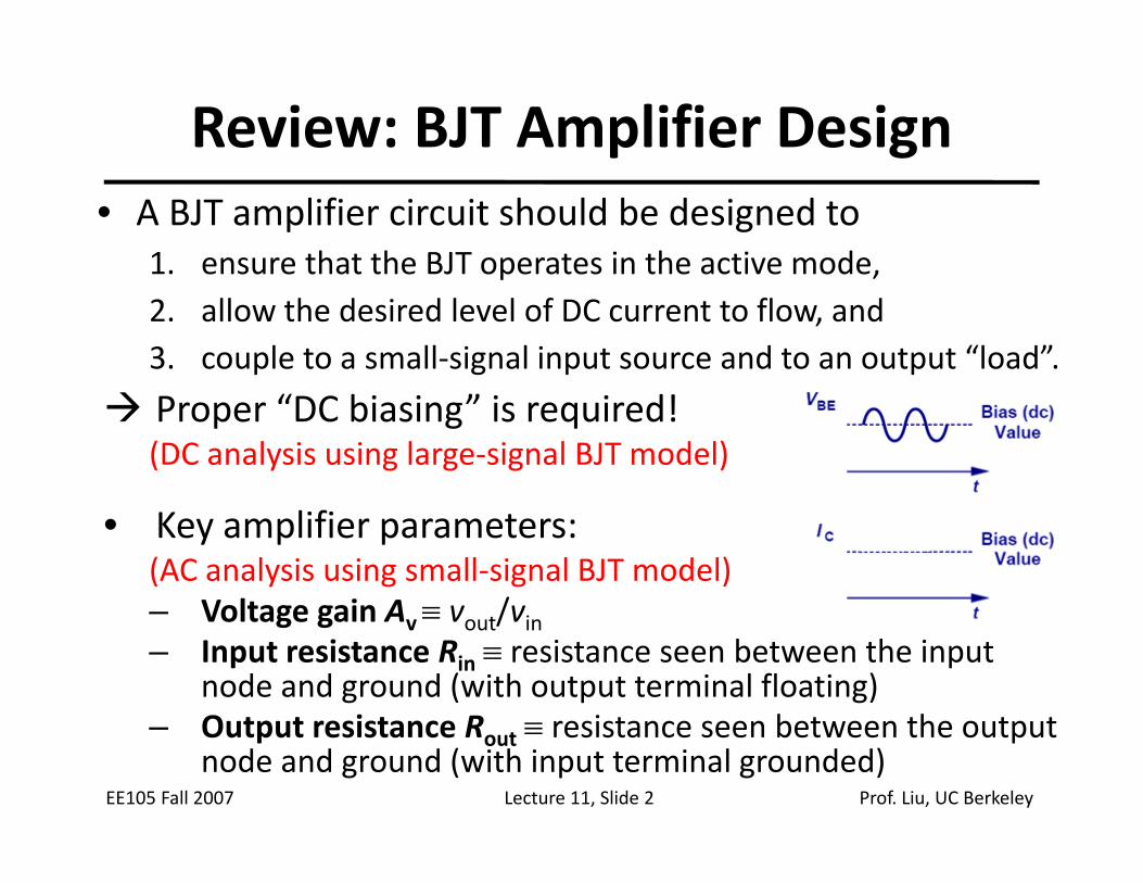
Review: BJT Amplifier Design• A BJT amplifier circuit should be designed to
1. ensure that the BJT operates in the active mode, p ,2. allow the desired level of DC current to flow, and3. couple to a small‐signal input source and to an output “load”.
Proper “DC biasing” is required!(DC analysis using large‐signal BJT model)
• Key amplifier parameters: (AC analysis using small‐signal BJT model)
Voltage gain A ≡ v /v– Voltage gain Av ≡ vout/vin– Input resistance Rin ≡ resistance seen between the input
node and ground (with output terminal floating)O t t i t R i t b t th t t
EE105 Fall 2007 Lecture 11, Slide 2 Prof. Liu, UC Berkeley
– Output resistance Rout ≡ resistance seen between the output node and ground (with input terminal grounded)

Large‐Signal vs. Small‐Signal Models• The large‐signal model is used to determine the DC operating point (VBE, VCE, IB, IC) of the BJT.p g p ( BE, CE, B, C)
• The small‐signal model is used to determine how the output responds to an input signal.
EE105 Fall 2007 Lecture 11, Slide 3 Prof. Liu, UC Berkeley

Small‐Signal Models for Independent Sources
• The voltage across an independent voltage source does not vary with time. (Its small‐signal voltage is always zero.)y ( g g y )
It is regarded as a short circuit for small‐signal analysis.
Large-Signal Small-SignalLarge-SignalModel
Small-SignalModel
• The current through an independent current source does not vary with time. (Its small‐signal current is always zero.)
It i d d i it f ll i l l i
EE105 Fall 2007 Lecture 11, Slide 4 Prof. Liu, UC Berkeley
It is regarded as an open circuit for small‐signal analysis.

Comparison of Amplifier TopologiesCommon Emitter
L A 0
Common Base
L A 0
Emitter Follower
0 A 1• Large Av < 0‐ Degraded by RE‐ Degraded by RB/(β+1)
• Large Av > 0‐Degraded by RE and RS‐ Degraded by RB/(β+1)
• 0 < Av ≤ 1‐ Degraded by RB/(β+1)
• Large Ri• Moderate Rin
‐ Increased by RB‐ Increased by RE(β+1)
• Small Rin‐ Increased by RB/(β+1)‐ Decreased by RE
Large Rin(due to RE(β+1))
• Small Rout y E(β )
• Rout ≅ RC
• ro degrades A , Ro t
y E
• Rout ≅ RC
• ro degrades A , Ro t
‐ Effect of source impedance is reduced by β+1D d b Rro degrades Av, Rout
but impedance seenlooking into the collector can be “boosted” by
ro degrades Av, Routbut impedance seenlooking into the collector can be “boosted” by
‐ Decreased by RE
• ro decreases Av, Rin, and Rout
EE105 Fall 2007 Lecture 11, Slide 5 Prof. Liu, UC Berkeley
yemitter degeneration
yemitter degeneration
and Rout
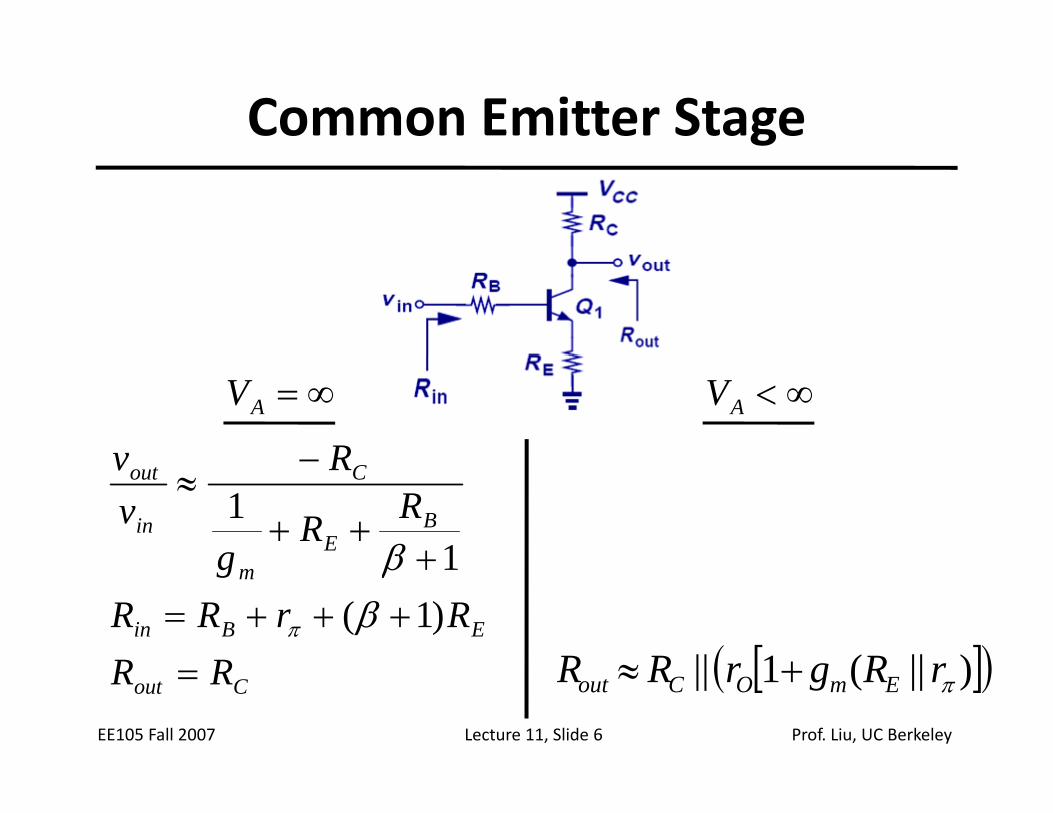
Common Emitter Stage
Rv
∞=AV ∞<AV
BE
C
in
out
RRg
Rvv
+++
−≈
11
β
EBin
m
RRRrRR
g+++=+)1(1
ββ
π
[ ]( ))||(1|| RRR +EE105 Fall 2007 Lecture 11, Slide 6 Prof. Liu, UC Berkeley
Cout RR = [ ]( ))||(1|| πrRgrRR EmOCout +≈
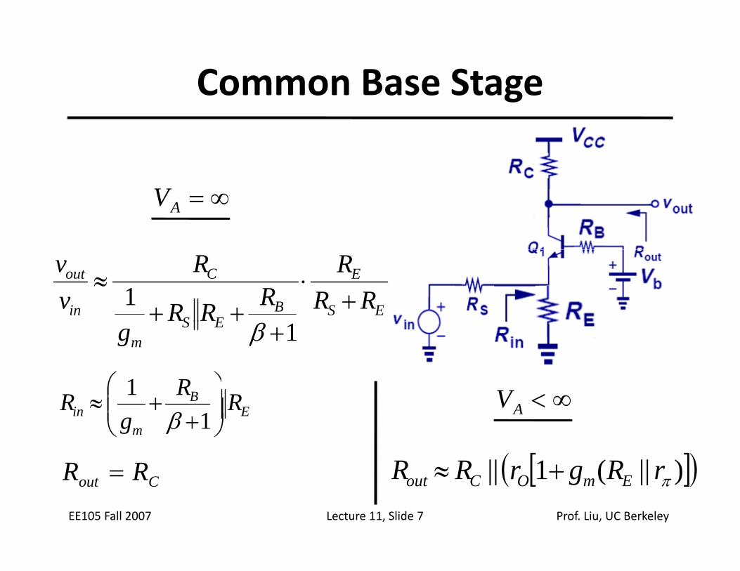
Common Base Stage
∞=AV
ES
E
BES
C
in
out
RRR
RRR
Rvv
+⋅
++≈ 1
ESmg +1β
BR ⎞⎜⎛ 1 VE
B
min RR
gR ⎟
⎠
⎞⎜⎜⎝
⎛+
+≈1
1β
RR [ ]( ))||(1|| RRR +
∞<AV
EE105 Fall 2007 Lecture 11, Slide 7 Prof. Liu, UC Berkeley
Cout RR = [ ]( ))||(1|| πrRgrRR EmOCout +≈

Emitter Follower
∞=AV ∞<AV
1= Eout
RRv OEout
RrRv
1||
=
11
+++β
S
mE
inR
gRv
RR )1( β ( )( )
S
mOE
in
RR
Rg
rRv
||11
1||+
++
ββ
Ein RrR )1( βπ ++=
s RRR ||1 ⎞⎜⎜⎛
+=
( )( )s
OEin
rRRR
rRrR
||||1
||1
⎞⎜⎜⎛
+=
++= βπ
EE105 Fall 2007 Lecture 11, Slide 8 Prof. Liu, UC Berkeley
Em
out Rg
R ||1⎠⎜⎜
⎝ ++=β OE
mout rR
gR ||||
1 ⎠⎜⎜⎝
++
=β

Ideal Current Source
Equivalent CircuitCircuit Symbol I-V Characteristic
• An ideal current source has infinite output impedance• An ideal current source has infinite output impedance.
How can we increase the output impedance of a BJT that d ?
EE105 Fall 2007 Lecture 11, Slide 9 Prof. Liu, UC Berkeley
is used as a current source?

Boosting the Output Impedance• Recall that emitter degeneration boosts the impedance seen looking into the collector.g– This improves the gain of the CE or CB amplifier. However, headroom is reduced.
( )[ ] rRrrRgR ||||1 ++=
EE105 Fall 2007 Lecture 11, Slide 10 Prof. Liu, UC Berkeley
( )[ ] ππ rRrrRgR EOEmout ||||1 ++=

Cascode Stage• In order to relax the trade‐off between output impedance and voltage headroom we can use aimpedance and voltage headroom, we can use a transistor instead of a degeneration resistor:
||)]||(1[ rrrrrgR ++=( )1211
12112
||||)]||(1[
π
ππ
rrrgRrrrrrgR
OOmout
OOOmout
≈++=
• V for Q can be as low as ~0 4V (“soft saturation”)
1 if 1212 >>≅= βCEC III
EE105 Fall 2007 Lecture 11, Slide 11 Prof. Liu, UC Berkeley
• VCE for Q2 can be as low as ~0.4V (“soft saturation”)

Maximum Cascode Output Impedance• The maximum output impedance of a cascode is limited by rlimited by rπ1.
rrrgR β≈
: If 12 πrrO >>
1111max, 1 OOmout rrrgR βπ=≈
EE105 Fall 2007 Lecture 11, Slide 12 Prof. Liu, UC Berkeley

PNP Cascode Stage
( )121121
||||)]||(1[ ππ
RrrrrrgR OOOmout ++=
EE105 Fall 2007 Lecture 11, Slide 13 Prof. Liu, UC Berkeley
( )1211 || πrrrgR OOmout ≈

False Cascodes• When the emitter of Q1 is connected to the emitter of Q it’s not a cascode since Q is a diode‐connectedQ2, it s not a cascode since Q2 is a diode connected device instead of a current source.
11 ⎤⎡ ⎞⎜⎛
1
122
1122
1
1
||||1||||11 Om
OOm
mout
g
rrg
rrrg
gR
⎞⎜⎛
+⎥⎦
⎤⎢⎣
⎡⎟⎠
⎞⎜⎜⎝
⎛+= ππ
EE105 Fall 2007 Lecture 11, Slide 14 Prof. Liu, UC Berkeley
12
12
1 211 Om
Om
mout r
gr
ggR ≈+⎟
⎠
⎞⎜⎜⎝
⎛+≈

Short‐Circuit Transconductance
• The short‐circuit transconductance of a circuit is a measure of its strength in converting an inputmeasure of its strength in converting an input voltage signal into an output current signal.
i
0=
≡outvin
outm v
iG
EE105 Fall 2007 Lecture 11, Slide 15 Prof. Liu, UC Berkeley

Voltage Gain of a Linear Circuit• By representing a linear circuit with its Norton equivalent the relationship between V and V canequivalent, the relationship between Vout and Vin can be expressed by the product of Gm and Rout.
Norton Equivalent Circuit
RvGRiv ==
outminout
outinmoutoutout
RGvvRvGRiv
−=−=−=Computation of
short-circuit output current:
EE105 Fall 2007 Lecture 11, Slide 16 Prof. Liu, UC Berkeley

Example: Determination of Voltage Gain Determination of Gm Determination of Rout
1out giG =≡ 1
x rvR =≡
rgA =
10
mvin
m gv
Gout
≡=
1ox
out ri
R ≡
EE105 Fall 2007 Lecture 11, Slide 17 Prof. Liu, UC Berkeley
11 Omv rgA −=
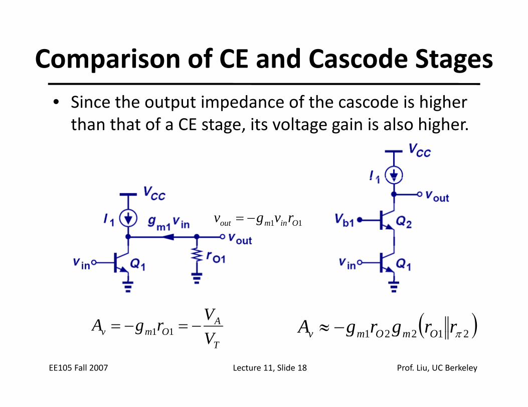
Comparison of CE and Cascode Stages• Since the output impedance of the cascode is higher than that of a CE stage its voltage gain is also higherthan that of a CE stage, its voltage gain is also higher.
11 Oinmout rvgv −=
AOmv
VrgA −=−= 11 ( )21221 rrgrgA OO−≈
EE105 Fall 2007 Lecture 11, Slide 18 Prof. Liu, UC Berkeley
TOmv V
g 11 ( )21221 πrrgrgA OmOmv

Voltage Gain of Cascode Amplifier• Since rO is much larger than 1/gm, most of IC,Q1 flows into diode‐connected Q2. Using Rout as before, AV is Q2 g out , V easily calculated.
11 it gGvgi =⇒= 11 mminmout gGvgi ⇒
outmv RGA −=( )( )[ ]
( )[ ]22121
2122121
||||||1
OOmm
OOOmm
rrrggrrrrrgg
π
ππ
−≈++−=
EE105 Fall 2007 Lecture 11, Slide 19 Prof. Liu, UC Berkeley
( )

Practical Cascode Stage• No current source is ideal; the output impedance is finite.
)||(|| rrrgrR ≈
EE105 Fall 2007 Lecture 11, Slide 20 Prof. Liu, UC Berkeley
)||(|| 21223 πrrrgrR OOmOout ≈

Improved Cascode Stage• In order to preserve the high output impedance, a cascode PNP current source is usedcascode PNP current source is used.
[ ] [ ][ ] [ ]outmv
OOmOOmout
RgArrrgrrrgR
1
21223433 )||(||)||(−=≈ ππ
EE105 Fall 2007 Lecture 11, Slide 21 Prof. Liu, UC Berkeley